Embed Size (px)
Citation preview
1
ELEKTRONIKA DASAR
Jurusan Teknik Elektro
FT-UGM
2007
Bahan Kuliah Minggu ke 6
2
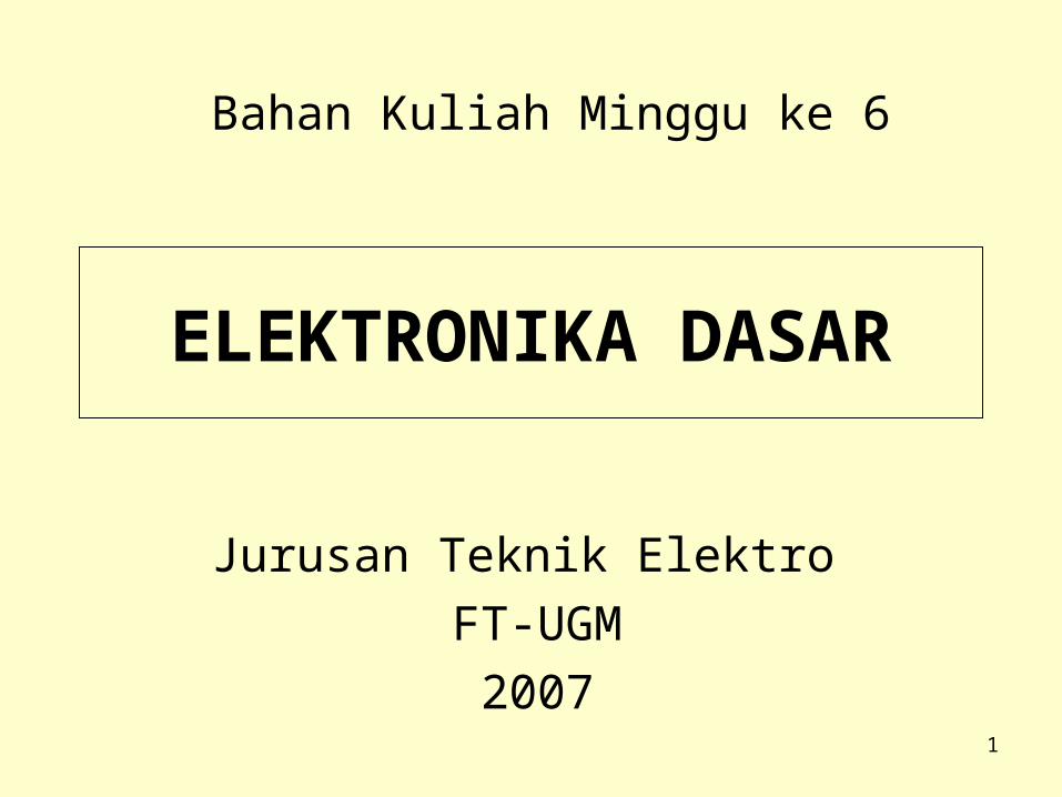
DIODA DAYA
V
I
Vbreakdown
Reverse biasregion
Forward biasregion
Anode Cathode
I
V
Diode symbol and ideal current–voltage characteristic.
Typical medium power diode
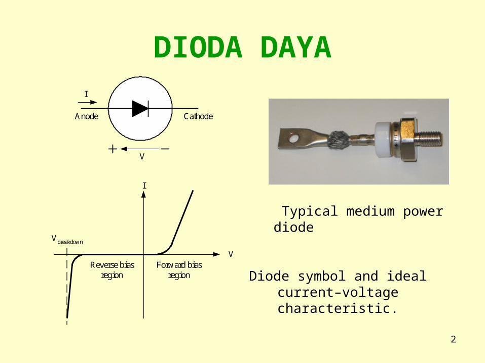
3
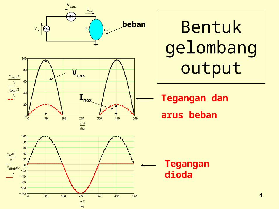
4
Bentuk gelombang
output
VloadVac
Iload
Rload
Vdiode
0 90 180 270 360 450 5400
20
40
60
80
100
Vload t( )
V
Iload t( )
A
t
deg
0 90 180 270 360 450 540100
80
60
40
20
0
20
40
60
80
100
Vac t( )
V
Vdiode t( )
V
t
deg
Tegangan dan
arus beban
Tegangan dioda
Vmax
Imax
beban
5
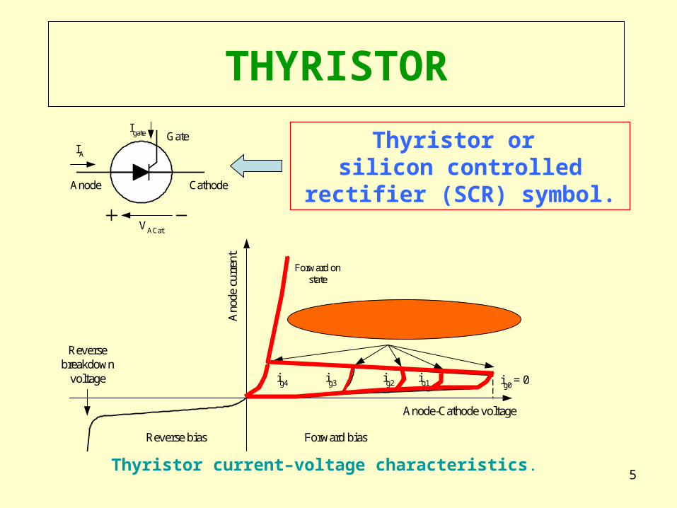
THYRISTOR
Gate
CathodeAnode
Igate
VACat
IAThyristor or
silicon controlled rectifier (SCR) symbol.
Forward onstate
Ano
de c
urre
nt
Anode-Cathode voltage
Reverse bias Forward bias
Reversebreakdown
voltage
Forward breakdown voltage (VFB) vs.gate current
ig0 = 0ig1ig2ig3ig4
Thyristor current–voltage characteristics.
6
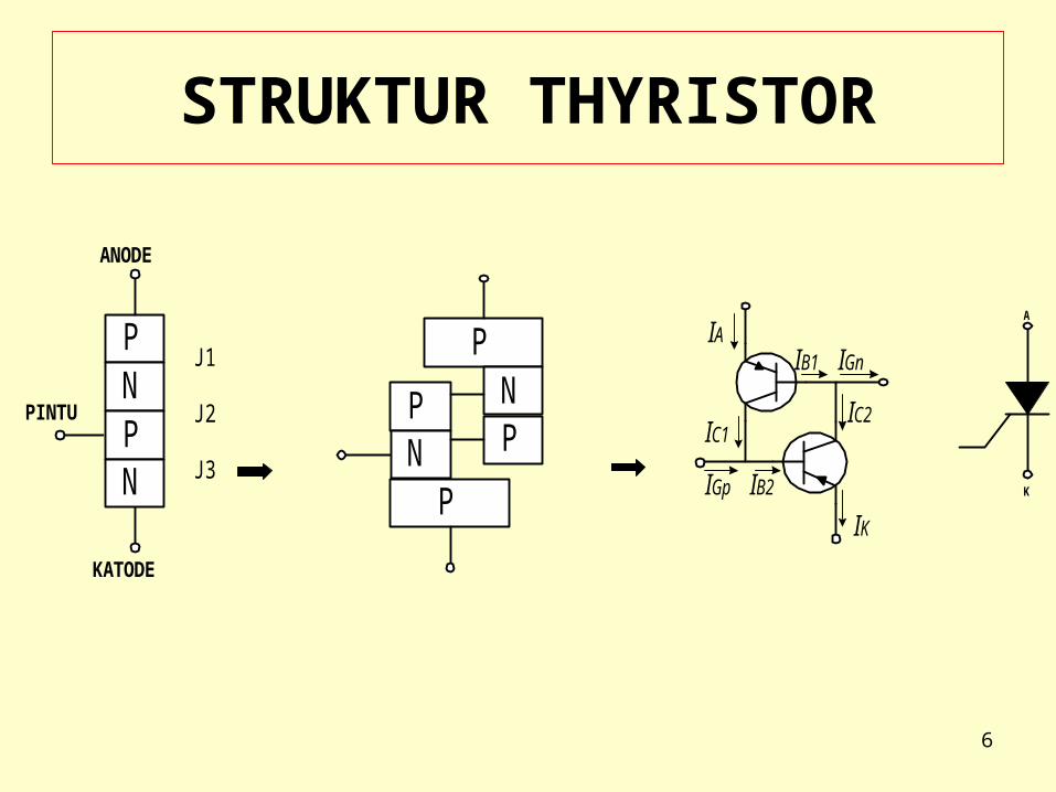
STRUKTUR THYRISTOR
ANODE
PINTU
KATODE
P
PN
P
PN
PNPN
IAIB1 IGn
IC2
IKIB2IGp
IC1
A
K
J1
J2
J3
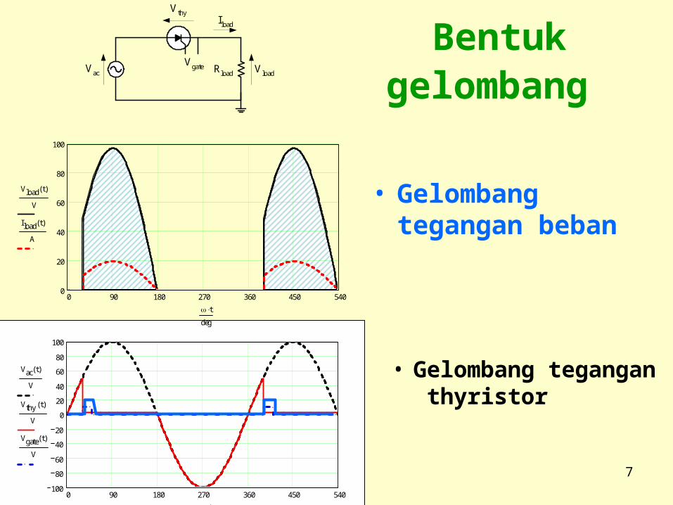
7
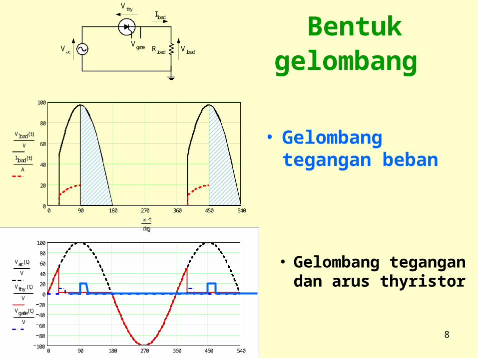
Bentuk gelombang
• Gelombang tegangan beban
Vgate Rload
Iload
Vac
Vthy
Vload
0 90 180 270 360 450 5400
20
40
60
80
100
Vload t( )
V
Iload t( )
A
t
deg
0 90 180 270 360 450 540100
80
60
40
20
0
20
40
60
80
100
Vac t( )
V
Vthy t( )
V
Vgate t( )
V
t
deg
• Gelombang tegangan thyristor
8
Bentuk gelombang
• Gelombang tegangan beban
Vgate Rload
Iload
Vac
Vthy
Vload
0 90 180 270 360 450 5400
20
40
60
80
100
Vload t( )
V
Iload t( )
A
t
deg
0 90 180 270 360 450 540100
80
60
40
20
0
20
40
60
80
100
Vac t( )
V
Vthy t( )
V
Vgate t( )
V
t
deg
• Gelombang tegangan dan arus thyristor
9
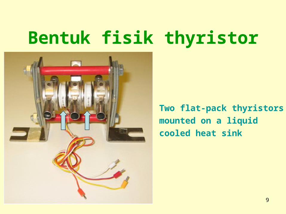
Bentuk fisik thyristor
Two flat-pack thyristors
mounted on a liquid
cooled heat sink
10
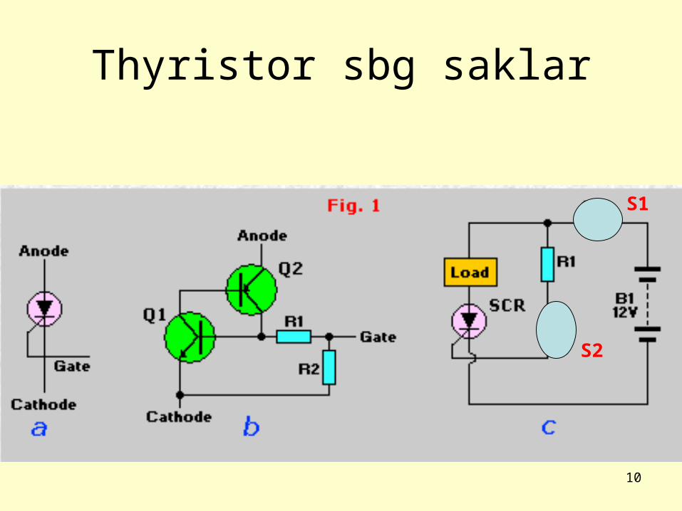
Thyristor sbg saklar
S1
S2
11
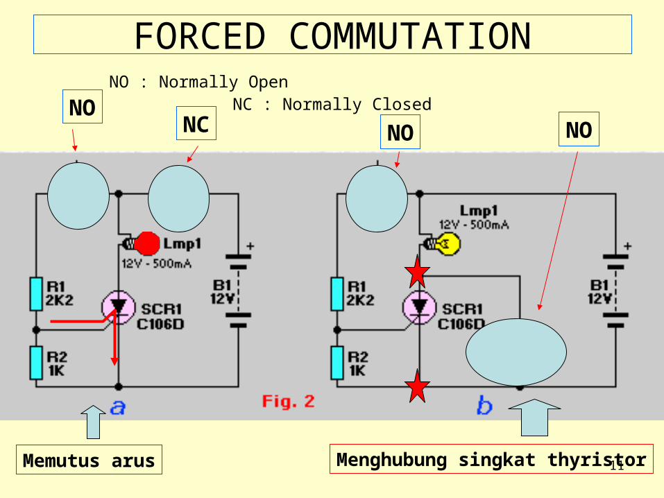
FORCED COMMUTATION
NONC NONO
Memutus arus Menghubung singkat thyristor
NO : Normally OpenNC : Normally Closed
12
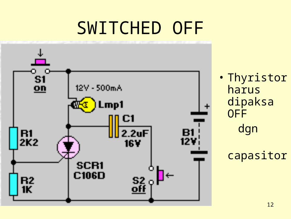
SWITCHED OFF
• Thyristor harus dipaksa OFF
dgn capasitor
13
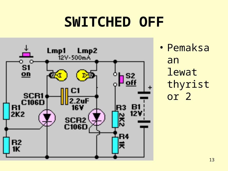
SWITCHED OFF
• Pemaksaan lewat thyristor 2
14
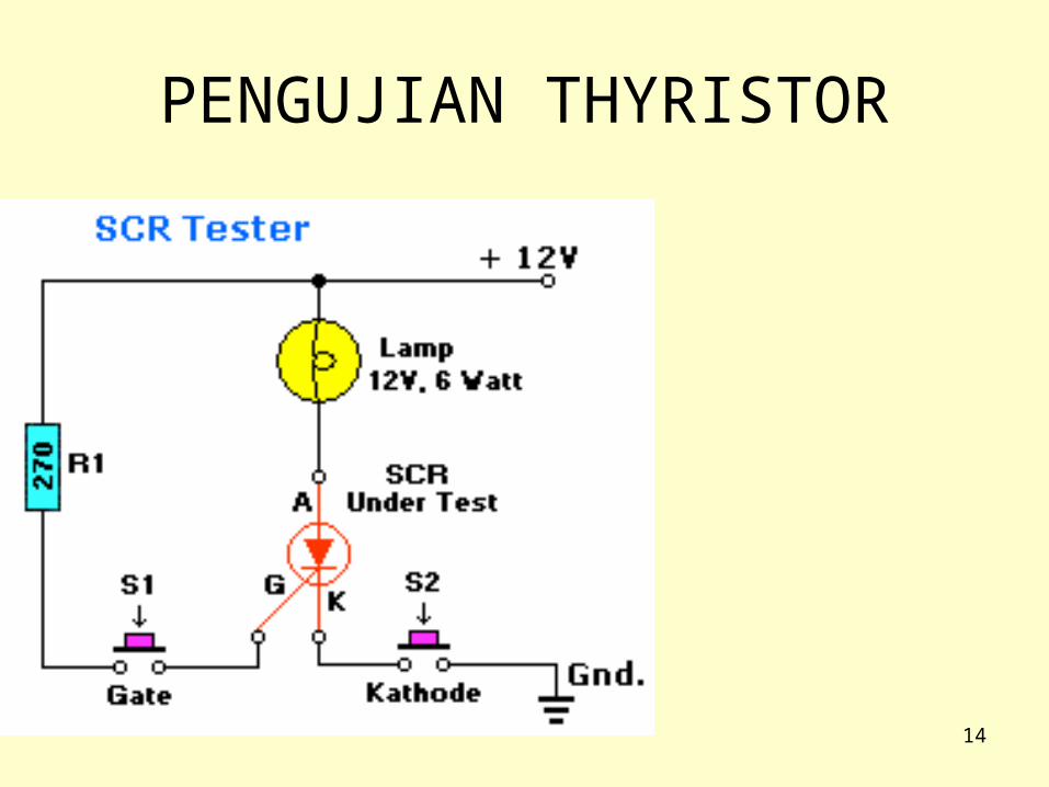
PENGUJIAN THYRISTOR
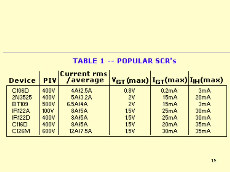
15
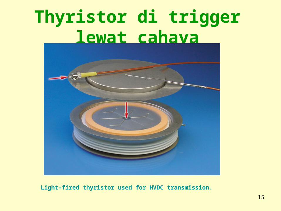
Thyristor di trigger lewat cahaya
Light-fired thyristor used for HVDC transmission.
16
17
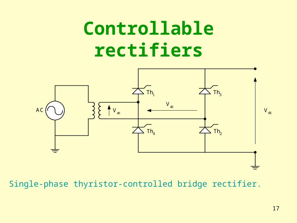
Controllable rectifiers
VacVdc
AC
Th4
Th1
Th2
Th3
Vac
Single-phase thyristor-controlled bridge rectifier.
18
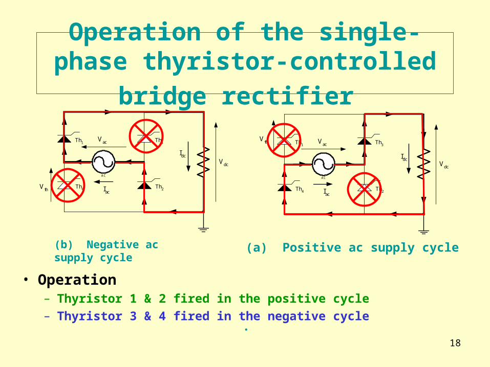
Operation of the single-phase
thyristor-controlled bridge rectifier
• Operation– Thyristor 1 & 2 fired in the positive cycle– Thyristor 3 & 4 fired in the negative cycle
Vth Iac
Idc
Vac
Vdc
Th4
Th1
Th2
Th3
AC
(a) Positive ac supply cycle
Vth
Iac
Idc
Vac
Vdc
AC
Th4
Th1
Th2
Th3
.
(b) Negative ac supply cycle
19
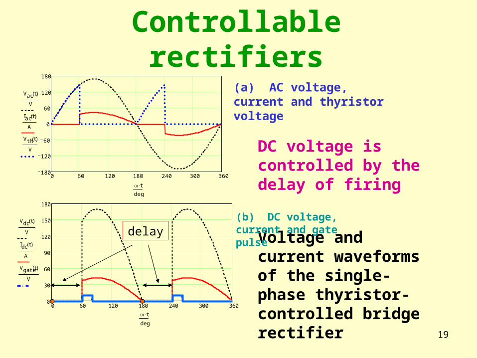
Controllable rectifiers
0 60 120 180 240 300 360180
120
60
0
60
120
180
Vac t( )
V
Iac t( )
A
Vth t( )
V
tdeg
(a) AC voltage, current and thyristor voltage
0 60 120 180 240 300 3600
30
60
90
120
150
180
Vdc t( )
V
Idc t( )
A
Vgate t( )
V
t
deg
Voltage and current waveforms of the single-phase thyristor-controlled bridge rectifier
(b) DC voltage, current and gate pulse
DC voltage is controlled by the delay of firing
delay
20
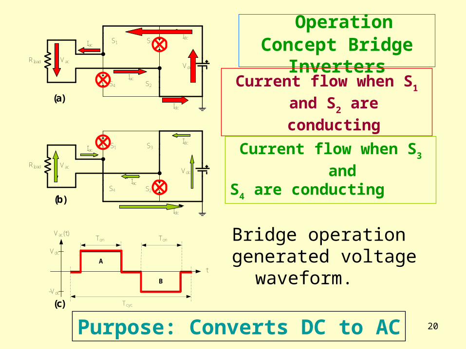
Operation Concept Bridge Inverters
TonVac(t)
t
B
A
Tcyc(c)
Ton
Vdc
-Vdc
Vdc
Vac
Idc
Rload
S1
S2
Iac
Iac
Idc
(b)S4
S3
Vdc
Vac
Idc
Rload
S1
S2
Iac
Iac
Idc
(a)
S3
S4
Purpose: Converts DC to AC
Current flow when S1 and
S2 are conducting
Bridge operationgenerated voltage waveform.
Current flow when S3 and
S4 are conducting
21
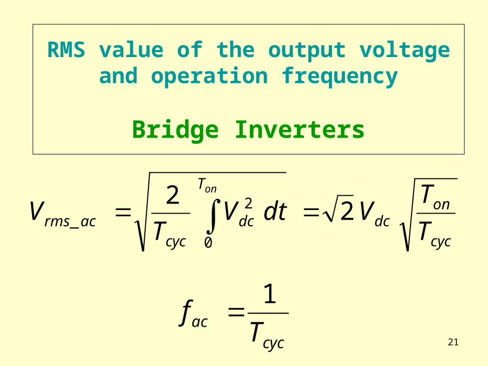
RMS value of the output voltage and operation frequency
Bridge Inverters
cyc
ondc
T
dccyc
acrms T
TVdtV
TV
on
22
0
2_
cycac Tf
1
22
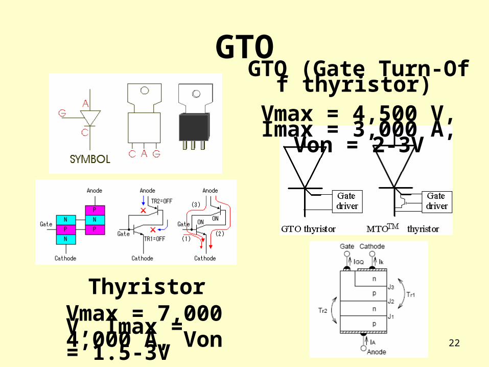
GTO
ThyristorVmax = 7,000 V, Imax = 4,000 A, Von = 1.5-3V
GTO ( -Gate Turn Of f thyristor)
Vmax = 4,500 V, Imax = 3,000 A,
Von = 2-3V
23
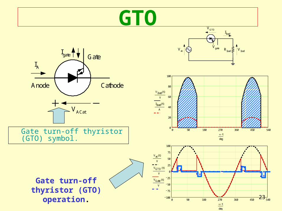
GTO
Gate turn-off thyristor (GTO) symbol.
Gate
CathodeAnode
Igate
VACat
IA
Vgate Rload
Iload
Vac
VGTO
Vload
0 90 180 270 360 450 5400
20
40
60
80
100
Vload t( )
V
Iload t( )
A
t
deg
0 90 180 270 360 450 540100
75
50
25
0
25
50
75
100
Vac t( )
V
VGTO t( )
V
VGate t( )
V
t
deg
Gate turn-off thyristor (GTO) operation.
24
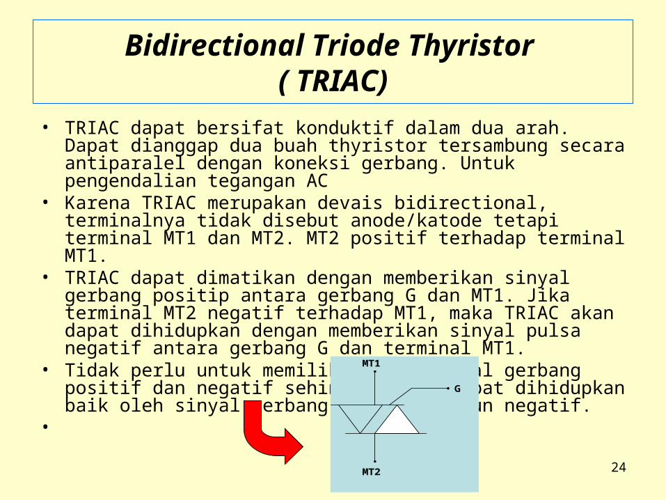
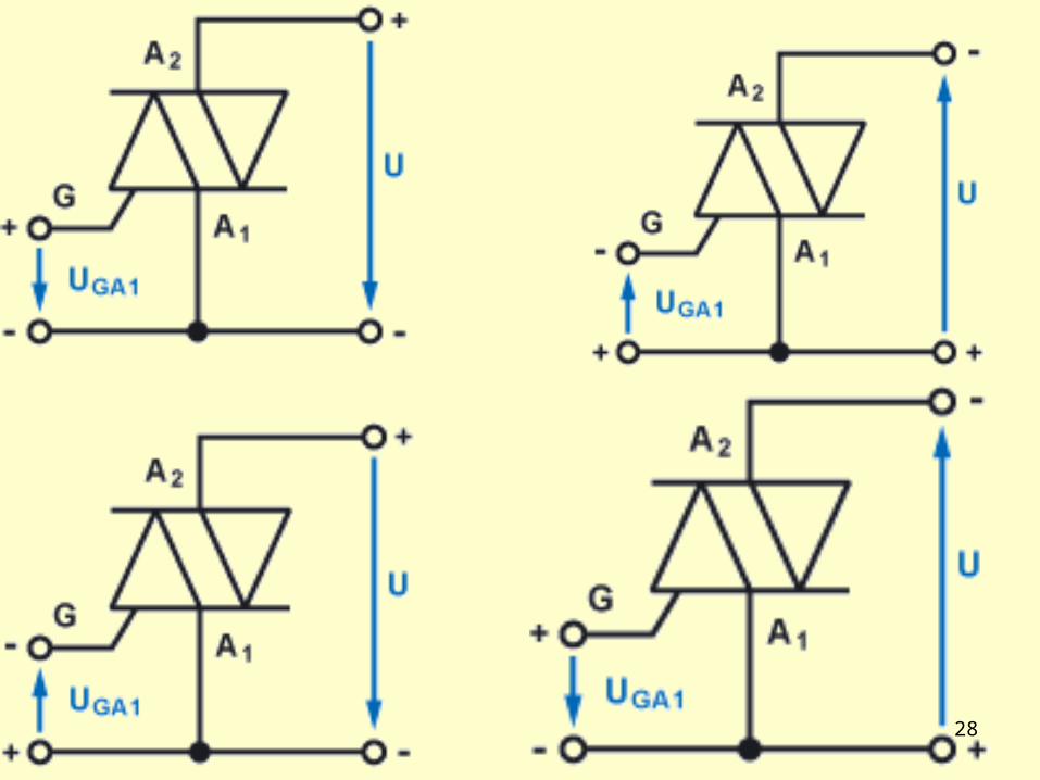
• TRIAC dapat bersifat konduktif dalam dua arah. Dapat dianggap dua buah thyristor tersambung secara antiparalel dengan koneksi gerbang. Untuk pengendalian tegangan AC
• Karena TRIAC merupakan devais bidirectional, terminalnya tidak disebut anode/katode tetapi terminal MT1 dan MT2. MT2 positif terhadap terminal MT1.
• TRIAC dapat dimatikan dengan memberikan sinyal gerbang positip antara gerbang G dan MT1. Jika terminal MT2 negatif terhadap MT1, maka TRIAC akan dapat dihidupkan dengan memberikan sinyal pulsa negatif antara gerbang G dan terminal MT1.
• Tidak perlu untuk memiliki kedua sinyal gerbang positif dan negatif sehingga TRIAC dapat dihidupkan baik oleh sinyal gerbang positif maupun negatif.
• Simbol TRIAC
Bidirectional Triode Thyristor ( TRIAC)
MT2
MT1
G
25
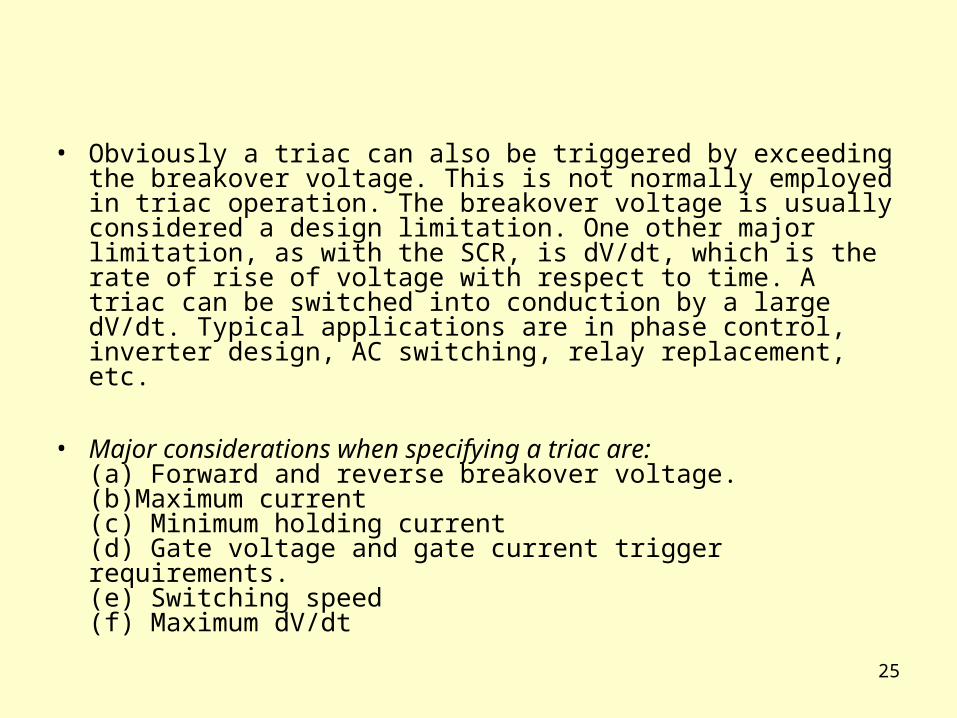
• Obviously a triac can also be triggered by exceeding the breakover voltage. This is not normally employed in triac operation. The breakover voltage is usually considered a design limitation. One other major limitation, as with the SCR, is dV/dt, which is the rate of rise of voltage with respect to time. A triac can be switched into conduction by a large dV/dt. Typical applications are in phase control, inverter design, AC switching, relay replacement, etc.
• Major considerations when specifying a triac are:(a) Forward and reverse breakover voltage.(b)Maximum current(c) Minimum holding current(d) Gate voltage and gate current trigger requirements.(e) Switching speed(f) Maximum dV/dt
26
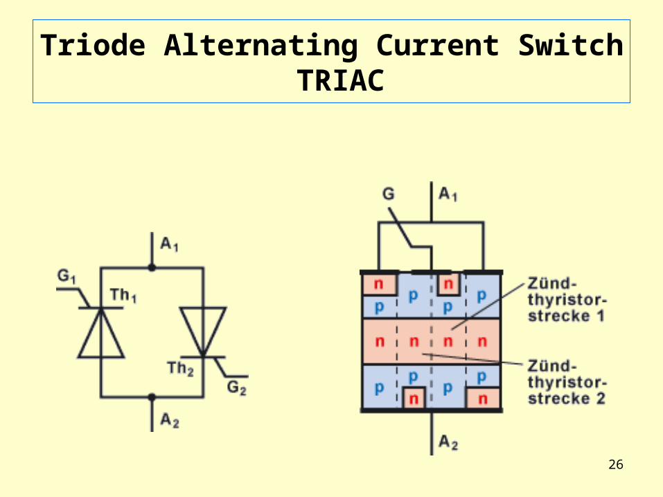
Triode Alternating Current Switch TRIAC
27
28
29
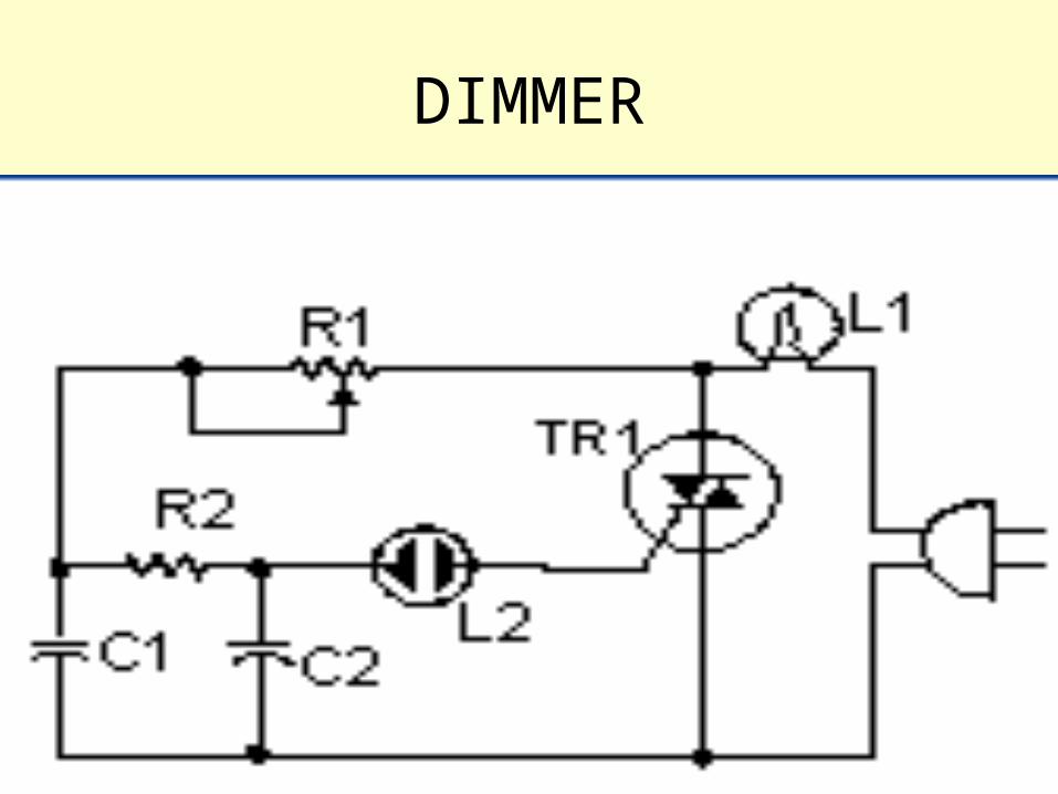
DIMMER
30
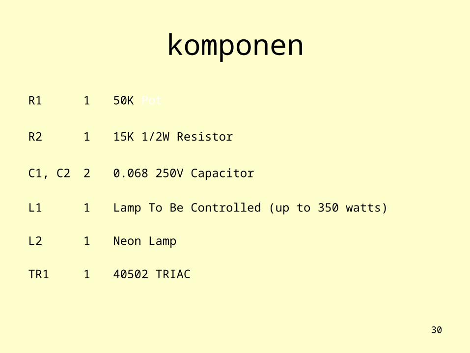
komponen
R1 1 50K Pot
R2 1 15K 1/2W Resistor
C1, C2 2 0.068 250V Capacitor
L1 1 Lamp To Be Controlled (up to 350 watts)
L2 1 Neon Lamp
TR1 1 40502 TRIAC
31
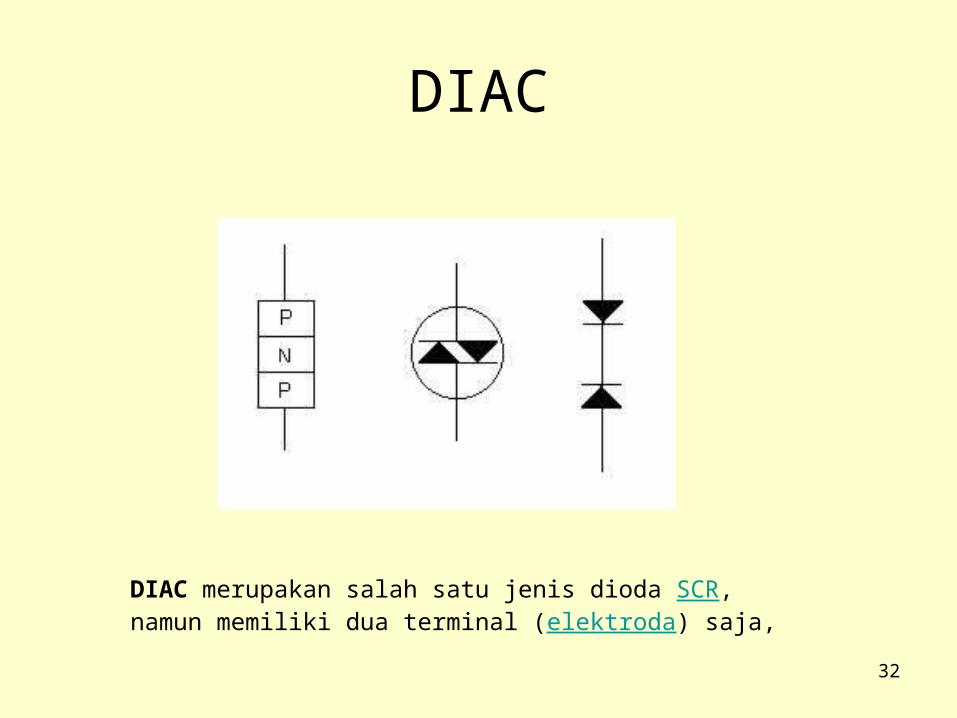
32
DIAC
DIAC merupakan salah satu jenis dioda SCR, namun memiliki dua terminal (elektroda) saja,
33
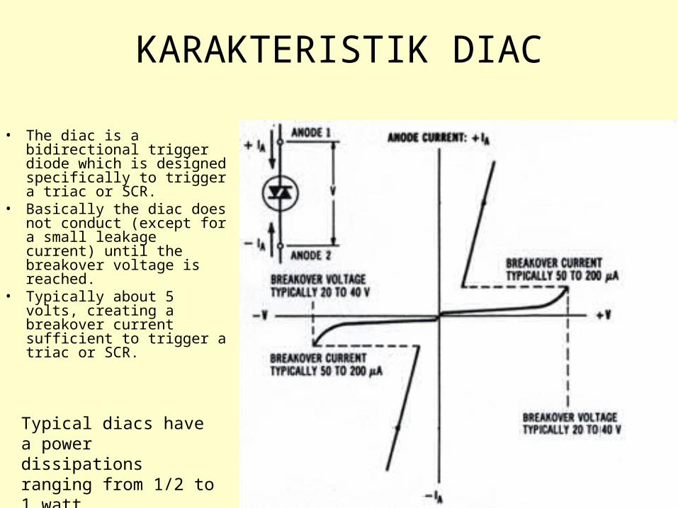
KARAKTERISTIK DIAC
• The diac is a bidirectional trigger diode which is designed specifically to trigger a triac or SCR.
• Basically the diac does not conduct (except for a small leakage current) until the breakover voltage is reached.
• Typically about 5 volts, creating a breakover current sufficient to trigger a triac or SCR.
Typical diacs have a power dissipations ranging from 1/2 to 1 watt.
34
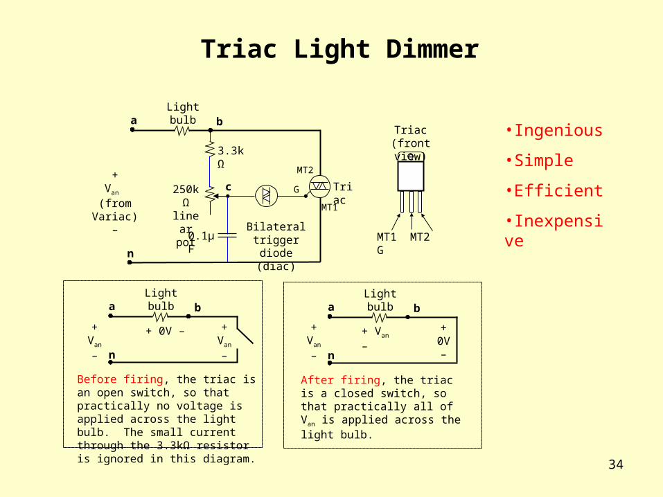
Triac Light Dimmer
Triac(front view)
MT1 MT2 G
+Van
(from Variac)–
Lightbulb
G
MT2
MT1
0.1µF
3.3kΩ
250kΩ linear pot
Triac
Bilateral trigger diode
(diac)
a
c
n
b
Lightbulba
n
b
Before firing, the triac is an open switch, so that practically no voltage is applied across the light bulb. The small current through the 3.3kΩ resistor is ignored in this diagram.
+ 0V –+Van
–
+Van
–
•Ingenious
•Simple
•Efficient
•Inexpensive
After firing, the triac is a closed switch, so that practically all of Van is applied across the light bulb.
Lightbulba
n
b
+ Van –+
Van
–
+0V–
35
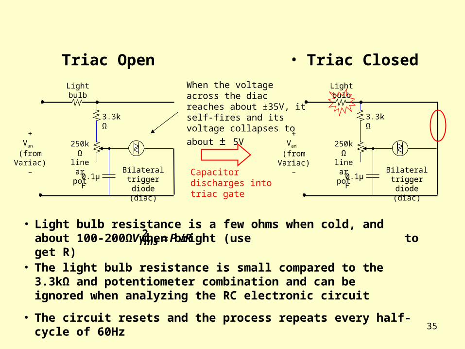
Triac Open
+Van
(from Variac)–
Lightbulb
0.1µF
3.3kΩ
250kΩ linear pot
Bilateral trigger diode
(diac)
• Light bulb resistance is a few ohms when cold, and about 100-200Ω when bright (use to get R)RPVrms /2
• The light bulb resistance is small compared to the 3.3kΩ and potentiometer combination and can be ignored when analyzing the RC electronic circuit
When the voltage across the diac reaches about ±35V, it self-fires and its voltage
collapses to about ± 5V
• The circuit resets and the process repeats every half-cycle of 60Hz
Capacitor discharges into triac gate
+Van
(from Variac)–
Lightbulb
0.1µF
3.3kΩ
250kΩ linear pot
Bilateral trigger diode
(diac)
• Triac Closed
36
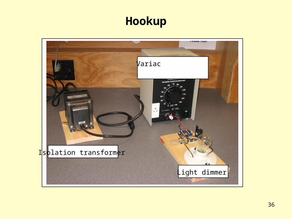
Hookup
Isolation transformer
Variac
Light dimmer
37
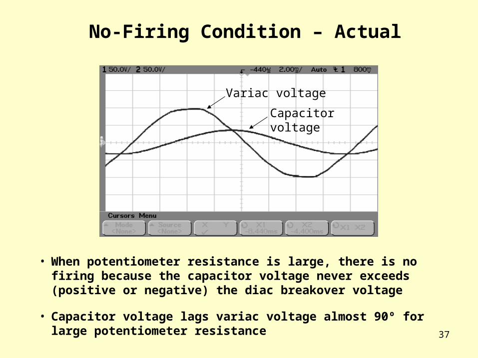
No-Firing Condition – Actual
• When potentiometer resistance is large, there is no firing because the capacitor voltage never exceeds (positive or negative) the diac breakover voltage
Variac voltage
Capacitor voltage
• Capacitor voltage lags variac voltage almost 90º for large potentiometer resistance
38
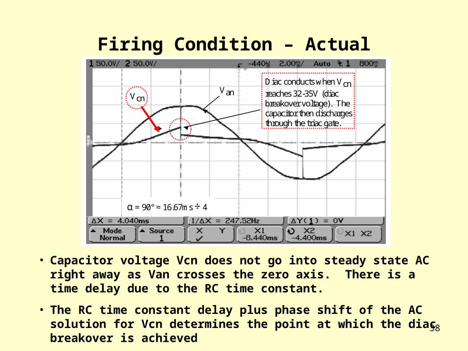
Firing Condition – Actual
• Capacitor voltage Vcn does not go into steady state AC right away as Van crosses the zero axis. There is a time delay due to the RC time constant.
• The RC time constant delay plus phase shift of the AC solution for Vcn determines the point at which the diac breakover is achieved
Van Vcn
α = 90° ≈ 16.67ms ÷ 4
Diac conducts when Vcn
reaches 32-35V (diac breakover voltage). The capacitor then discharges through the triac gate.
39
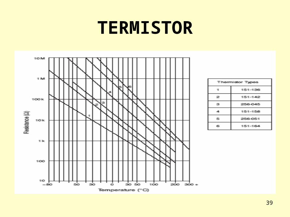
TERMISTOR
40
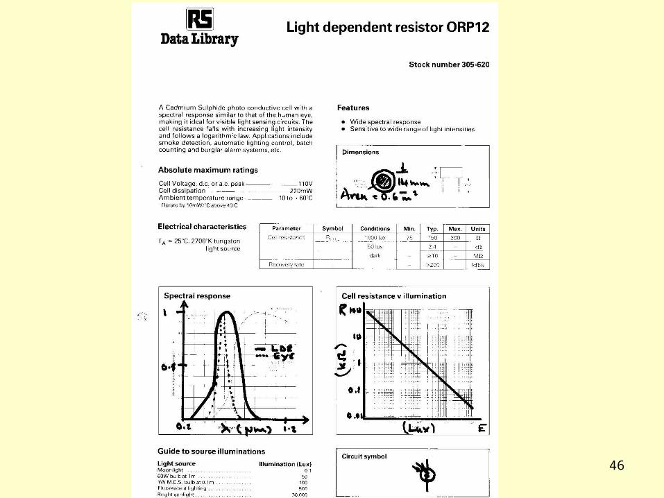
Light-dependent resistors• The simplest of the photoconductive devices is the
light-dependent resistor or LDR.• It is typically used in a voltage divider circuit. • LDRs are cheap and simple to use, but are slow to
respond to changes in light intensity and are often not suitable for high-speed computer applications.
• Due to its relatively large size and power requirements, the LDR tends not to be used for data signal production, but it has a use in applications such as simple alarm circuits and detectors on production lines.
41
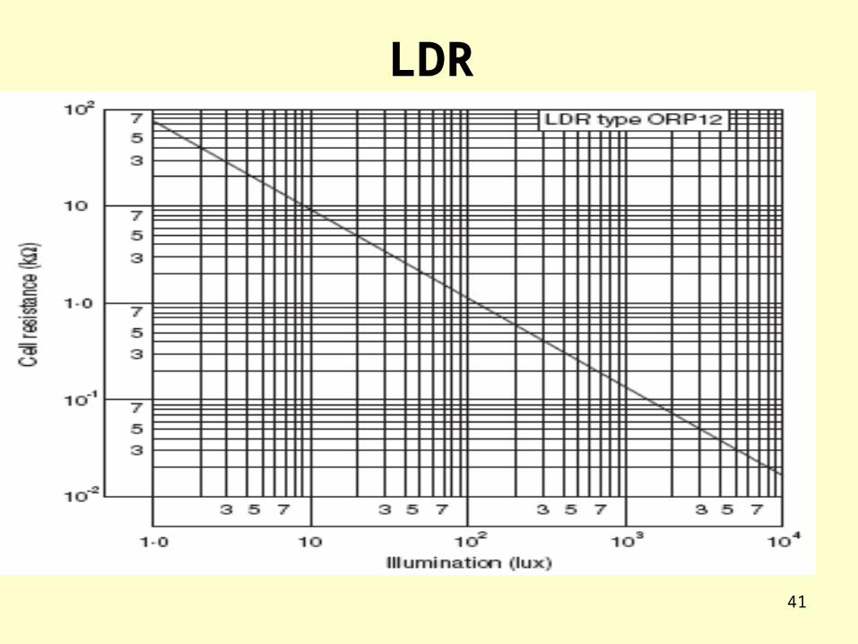
LDR
42
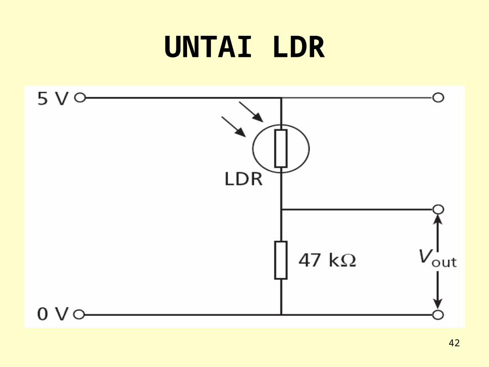
UNTAI LDR
43
44
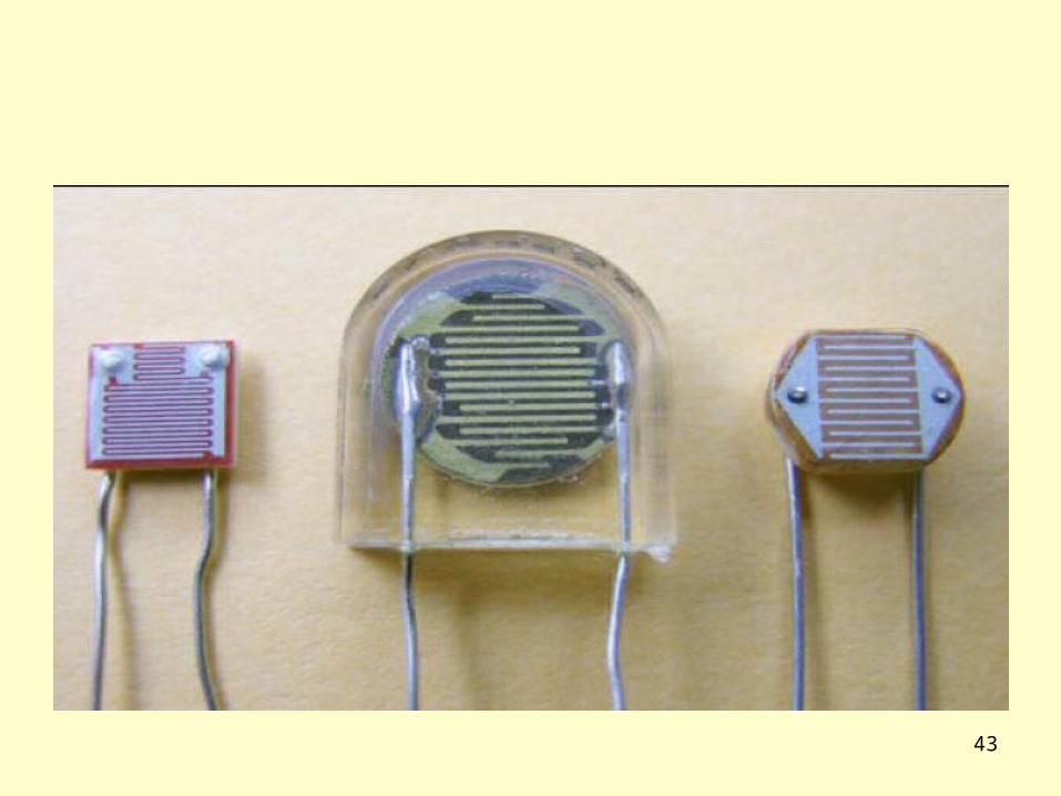
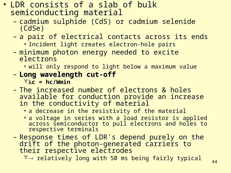
• LDR consists of a slab of bulk semiconducting material– cadmium sulphide (CdS) or cadmium selenide (CdSe)– a pair of electrical contacts across its ends
• Incident light creates electron-hole pairs– minimum photon energy needed to excite electrons
• will only respond to light below a maximum value– Long wavelength cut-offLong wavelength cut-off
c = hc/Wmin– The increased number of electrons & holes available
for conduction provide an increase in the conductivity of material
• a decrease in the resistivity of the material• a voltage in series with a load resistor is applied across
semiconductor to pull electrons and holes to respective terminals
– Response times of LDR's depend purely on the drift of the photon-generated carriers to their respective electrodes relatively long with 50 ms being fairly typical
45
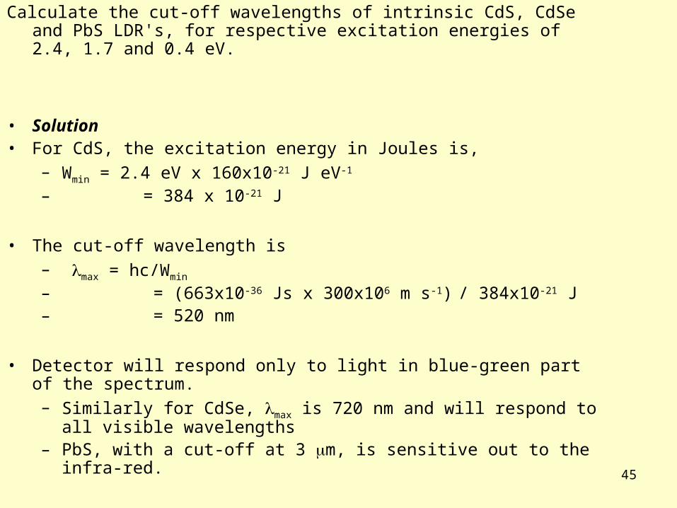
Calculate the cut-off wavelengths of intrinsic CdS, CdSe and PbS LDR's, for respective excitation energies of 2.4, 1.7 and 0.4 eV.
• Solution• For CdS, the excitation energy in Joules is,
– Wmin = 2.4 eV x 160x10-21 J eV-1
– = 384 x 10-21 J
• The cut-off wavelength is– max = hc/Wmin
– = (663x10-36 Js x 300x106 m s-1) / 384x10-21 J– = 520 nm
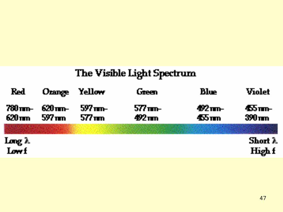
• Detector will respond only to light in blue-green part of the spectrum.– Similarly for CdSe, max is 720 nm and will respond to all visible
wavelengths– PbS, with a cut-off at 3 m, is sensitive out to the infra-red.
46
47
48
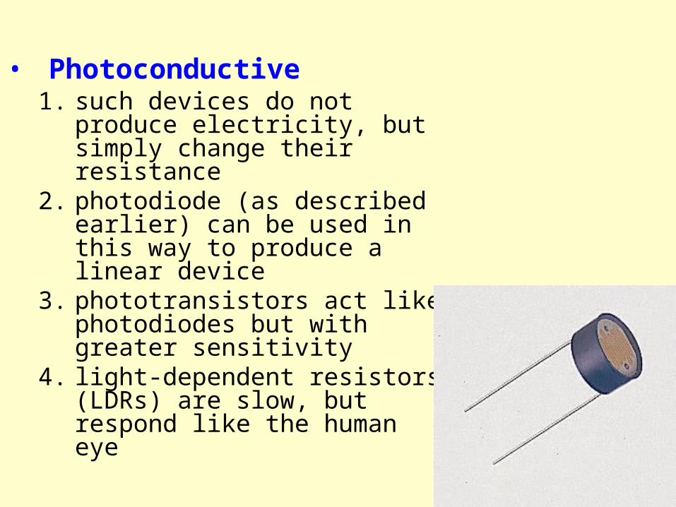
• Photoconductive1. such devices do not produce
electricity, but simply change their resistance
2. photodiode (as described earlier) can be used in this way to produce a linear device
3. phototransistors act like photodiodes but with greater sensitivity
4. light-dependent resistors (LDRs) are slow, but respond like the human eye