Embed Size (px)
Citation preview
Professor N Cheung, U.C. Berkeley
Lecture 13EE143 S06
1
Vacuum Basics
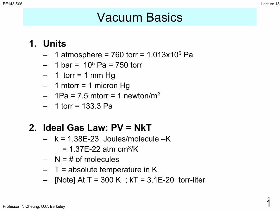
1. Units– 1 atmosphere = 760 torr = 1.013x10⁵ Pa– 1 bar = 105 Pa = 750 torr– 1 torr = 1 mm Hg– 1 mtorr = 1 micron Hg – 1Pa = 7.5 mtorr = 1 newton/m2
– 1 torr = 133.3 Pa
2. Ideal Gas Law: PV = NkT– k = 1.38E-23 Joules/molecule –K
= 1.37E-22 atm cm3/K– N = # of molecules– T = absolute temperature in K– [Note] At T = 300 K ; kT = 3.1E-20 torr-liter
1
Professor N Cheung, U.C. Berkeley
Lecture 13EE143 S06
2
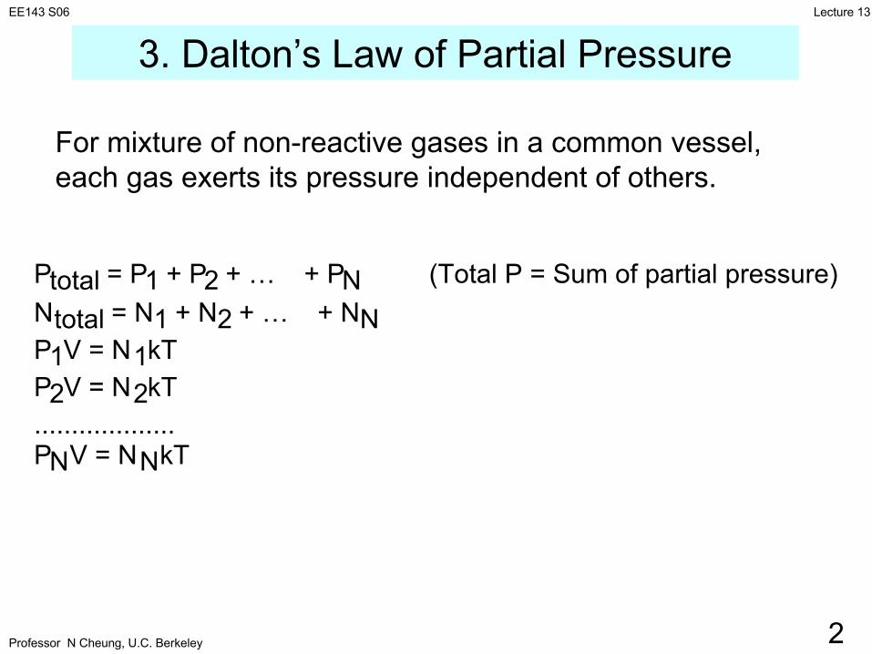
For mixture of non-reactive gases in a common vessel, each gas exerts its pressure independent of others.
Ptotal = P1 + P2 + … + PN (Total P = Sum of partial pressure)Ntotal = N1 + N2 + … + NNP1V = N1kTP2V = N2kT...................PNV = NNkT
3. Dalton’s Law of Partial Pressure
Professor N Cheung, U.C. Berkeley
Lecture 13EE143 S06
3
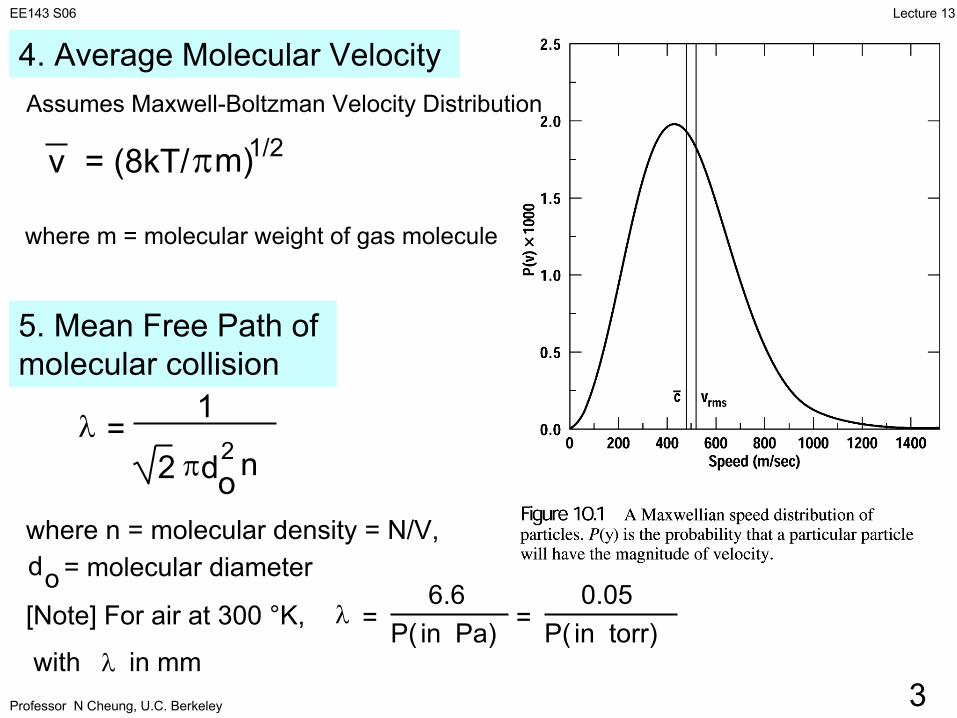
4. Average Molecular Velocity
v = (8kT/πm)1/2
where m = molecular weight of gas molecule
5. Mean Free Path of molecular collision
λ = 1
2 πd2o n
where n = molecular density = N/V,do = molecular diameter
[Note] For air at 300 °K, λ = 6.6
P( in Pa) = 0.05
P( in torr)with λ in mm
Assumes Maxwell-Boltzman Velocity Distribution
Professor N Cheung, U.C. Berkeley
Lecture 13EE143 S06
4
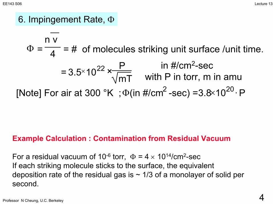
6. Impingement Rate, Φ
Φ = n v
4 = # of molecules striking unit surface /unit time.
= 3.5×10²² × PmT
in #/cm2-secwith P in torr, m in amu
[Note] For air at 300 °K ; Φ(in #/cm2 -sec) = 3.8×10²⁰ ⋅P
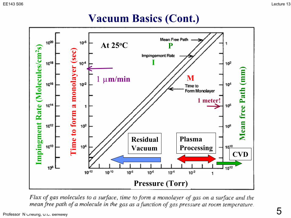
Example Calculation : Contamination from Residual Vacuum
For a residual vacuum of 10-6 torr, Φ = 4 × 10¹⁴/cm2-secIf each striking molecule sticks to the surface, the equivalent deposition rate of the residual gas is ~ 1/3 of a monolayer of solid per second.
Professor N Cheung, U.C. Berkeley
Lecture 13EE143 S06
5
Pressure (Torr)
Tim
e to
form
a m
onol
ayer
(sec
)
Impi
ngm
entR
ate
(Mol
ecul
es/c
m2 s
)
Mea
n fr
ee P
ath
(mm
)
At 25oC
M
I
P
1 meter!
1 µm/min
Vacuum Basics (Cont.)
ResidualVacuum
Plasma Processing
CVD
Professor N Cheung, U.C. Berkeley
Lecture 13EE143 S06
6
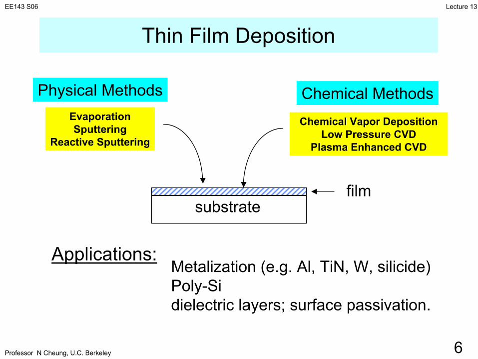
Thin Film Deposition
substratefilm
Applications:Metalization (e.g. Al, TiN, W, silicide)Poly-Sidielectric layers; surface passivation.
EvaporationSputtering
Reactive Sputtering
Chemical Vapor DepositionLow Pressure CVD
Plasma Enhanced CVD
Physical Methods Chemical Methods
Professor N Cheung, U.C. Berkeley
Lecture 13EE143 S06
7
(1) Evaporation Deposition
Al film
wafer
Al vapor
Al
hot heatingboat (e.g. W)
I
electronsource
crucible is water cooled
Al vapor
=PmkT2π
P P eHkT=
−
0∆
Vapor PressureEvaporation Rate (max)
m=molecular weight of vapor molecule
Log P
1/T
e
Vacuum Torr< 10 -5
Professor N Cheung, U.C. Berkeley
Lecture 13EE143 S06
8
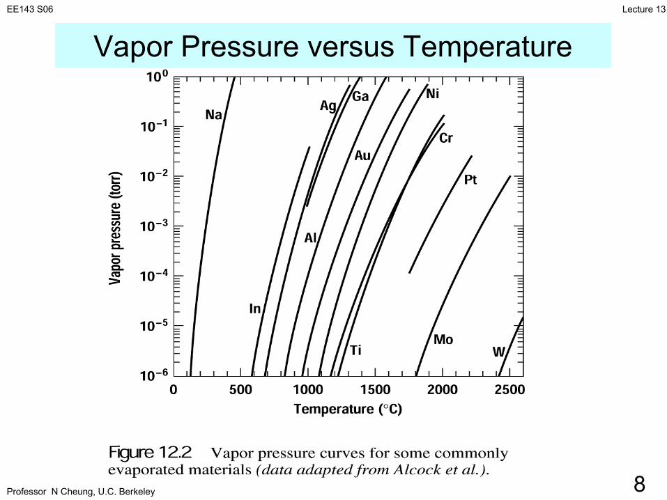
Vapor Pressure versus Temperature
Professor N Cheung, U.C. Berkeley
Lecture 13EE143 S06
9
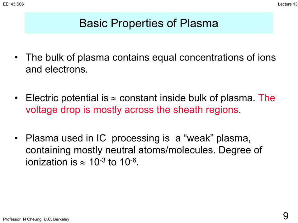
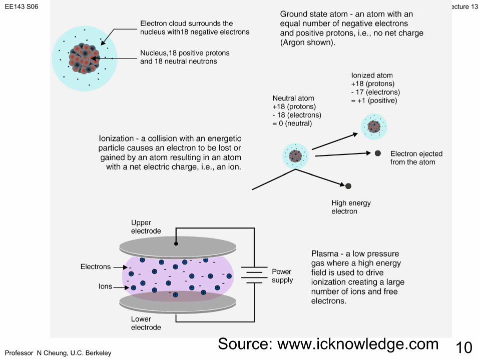
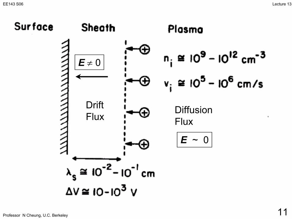
Basic Properties of Plasma
• The bulk of plasma contains equal concentrations of ions and electrons.
• Electric potential is ≈ constant inside bulk of plasma. The voltage drop is mostly across the sheath regions.
• Plasma used in IC processing is a “weak” plasma, containing mostly neutral atoms/molecules. Degree of ionization is ≈ 10-3 to 10-6.
Professor N Cheung, U.C. Berkeley
Lecture 13EE143 S06
10Source: www.icknowledge.com
Professor N Cheung, U.C. Berkeley
Lecture 13EE143 S06
11
DiffusionFlux
DriftFlux
E ≠ 0
E ~ 0
Professor N Cheung, U.C. Berkeley
Lecture 13EE143 S06
12
Al
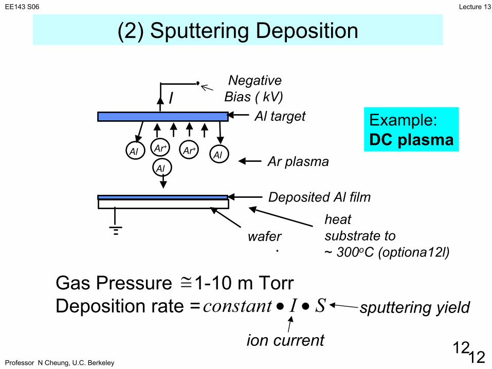
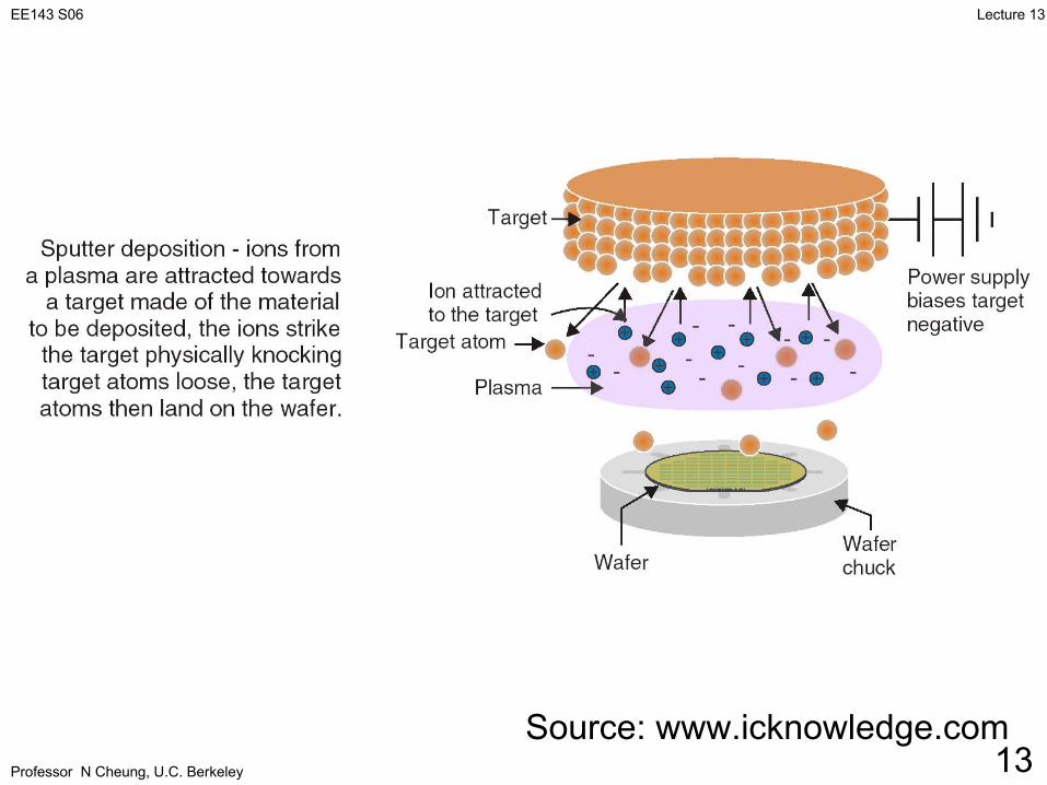
(2) Sputtering Deposition
Al AlAr+
Deposited Al film
Al target
Ar plasma
waferheat substrate to ~ 300oC (optiona12l)
Negative Bias ( kV)
⋅
I
Gas Pressure 1-10 m TorrDeposition rate =
≅sputtering yield
ion current
constant I S• •
Ar+
Example:DC plasma
12
Professor N Cheung, U.C. Berkeley
Lecture 13EE143 S06
13Source: www.icknowledge.com
Professor N Cheung, U.C. Berkeley
Lecture 13EE143 S06
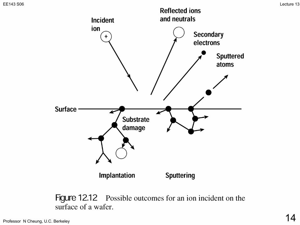
14
Professor N Cheung, U.C. Berkeley
Lecture 13EE143 S06
15
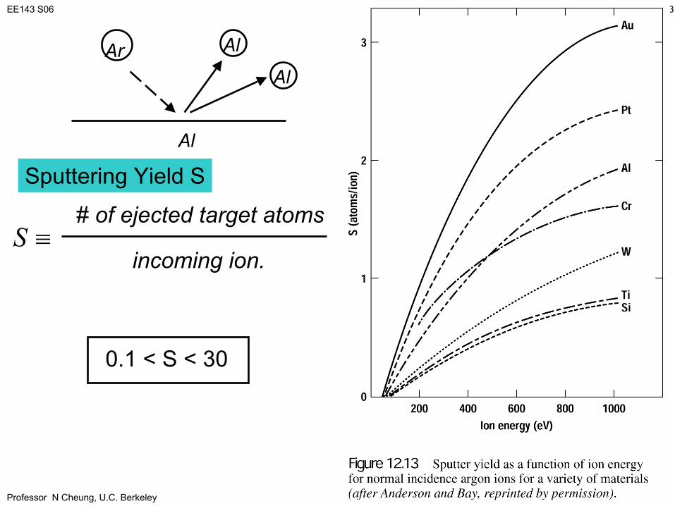
S ≡# of ejected target atoms
incoming ion.
0.1 < S < 30
Al
Al
Al
Ar
Sputtering Yield S
Professor N Cheung, U.C. Berkeley
Lecture 13EE143 S06
16
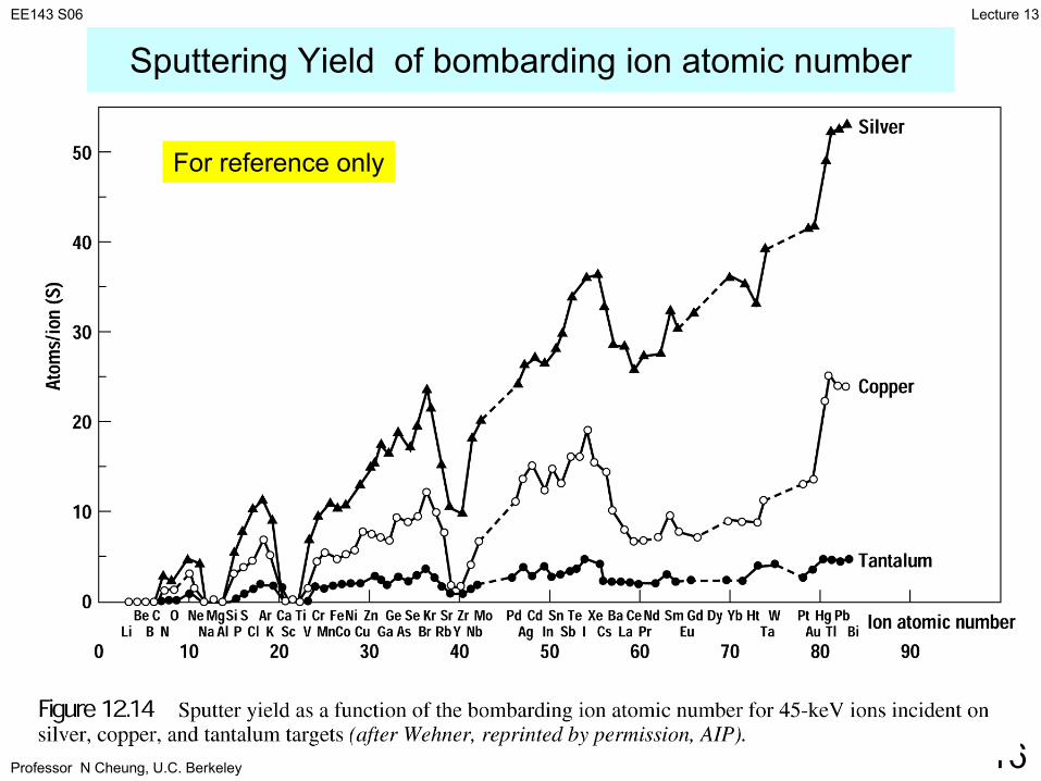
Sputtering Yield of bombarding ion atomic number
For reference only
Professor N Cheung, U.C. Berkeley
Lecture 13EE143 S06
17
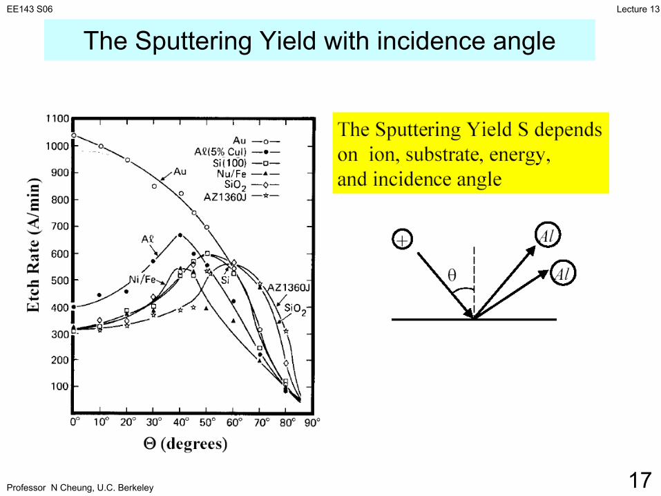
The Sputtering Yield with incidence angle
Professor N Cheung, U.C. Berkeley
Lecture 13EE143 S06
18
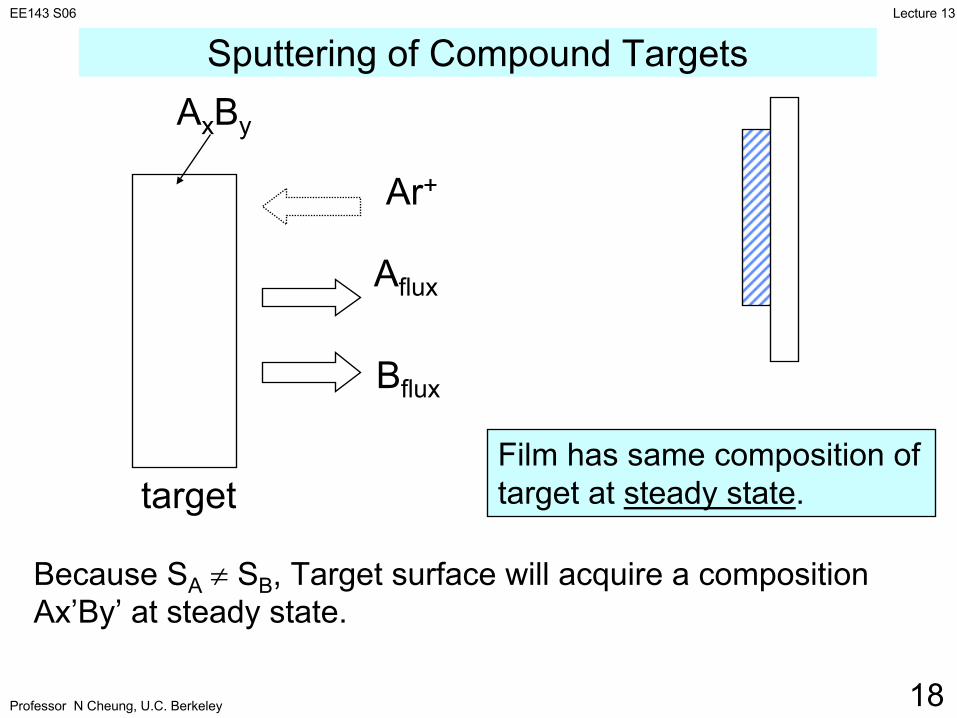
Ar+
Aflux
Bflux
AxBy
targetFilm has same composition of target at steady state.
Because SA ≠ SB, Target surface will acquire a composition Ax’By’ at steady state.
Sputtering of Compound Targets
Professor N Cheung, U.C. Berkeley
Lecture 13EE143 S06
19
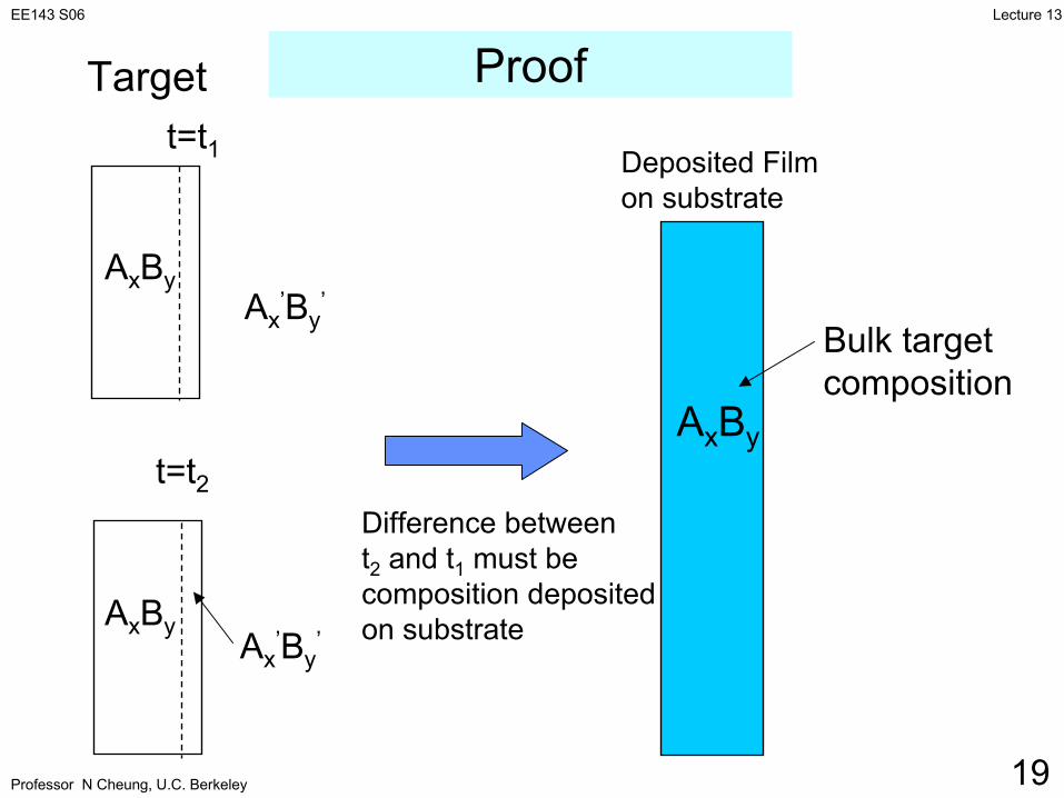
Target
AxBy
Deposited Film on substrate
AxBy
AxBy
Ax’By
’
Ax’By
’
t=t1
t=t2Difference betweent2 and t1 must becomposition depositedon substrate
Bulk target composition
Proof
Professor N Cheung, U.C. Berkeley
Lecture 13EE143 S06
20
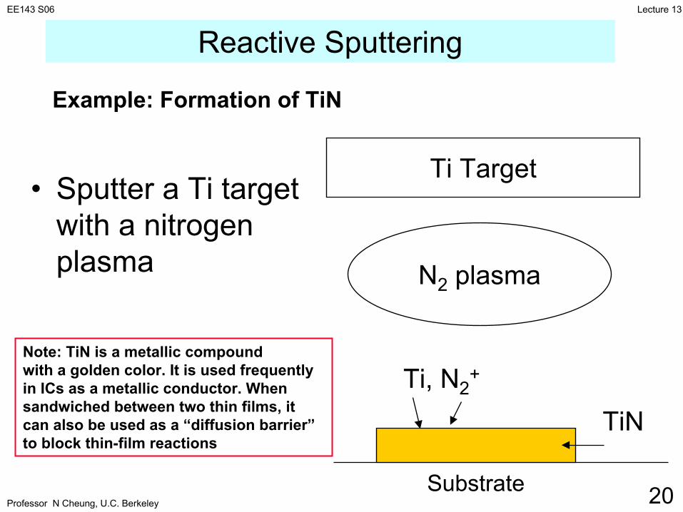
Reactive Sputtering
• Sputter a Ti target with a nitrogen plasma
Ti Target
N2 plasma
Ti, N2+
TiN
Example: Formation of TiN
Substrate
Note: TiN is a metallic compoundwith a golden color. It is used frequentlyin ICs as a metallic conductor. When sandwiched between two thin films, it can also be used as a “diffusion barrier” to block thin-film reactions
Professor N Cheung, U.C. Berkeley
Lecture 13EE143 S06
21
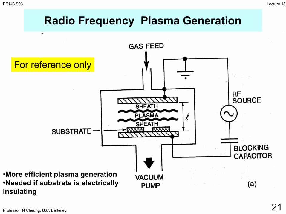
Radio Frequency Plasma Generation
For reference only
•More efficient plasma generation•Needed if substrate is electricallyinsulating
Professor N Cheung, U.C. Berkeley
Lecture 13EE143 S06
22
Professor N Cheung, U.C. Berkeley
Lecture 13EE143 S06
23
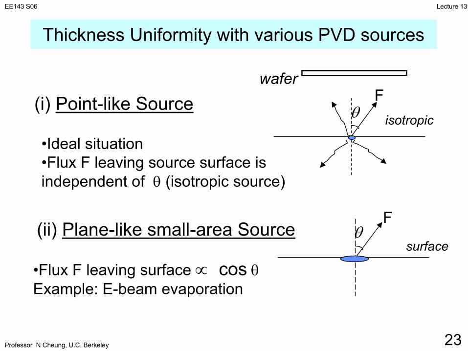
Thickness Uniformity with various PVD sources
(i) Point-like Source
(ii) Plane-like small-area SourceF
θsurface
θ
wafer
isotropic
•Ideal situation•Flux F leaving source surface isindependent of θ (isotropic source)
F
•Flux F leaving surface ∝ cos θExample: E-beam evaporation
Professor N Cheung, U.C. Berkeley
Lecture 13EE143 S06
24
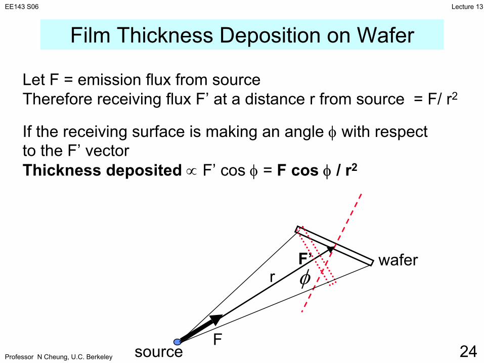
Let F = emission flux from sourceTherefore receiving flux F’ at a distance r from source = F/ r2
If the receiving surface is making an angle φ with respect to the F’ vectorThickness deposited ∝ F’ cos φ = F cos φ / r2
Film Thickness Deposition on Wafer
F
F’
source
waferφr
Professor N Cheung, U.C. Berkeley
Lecture 13EE143 S06
25
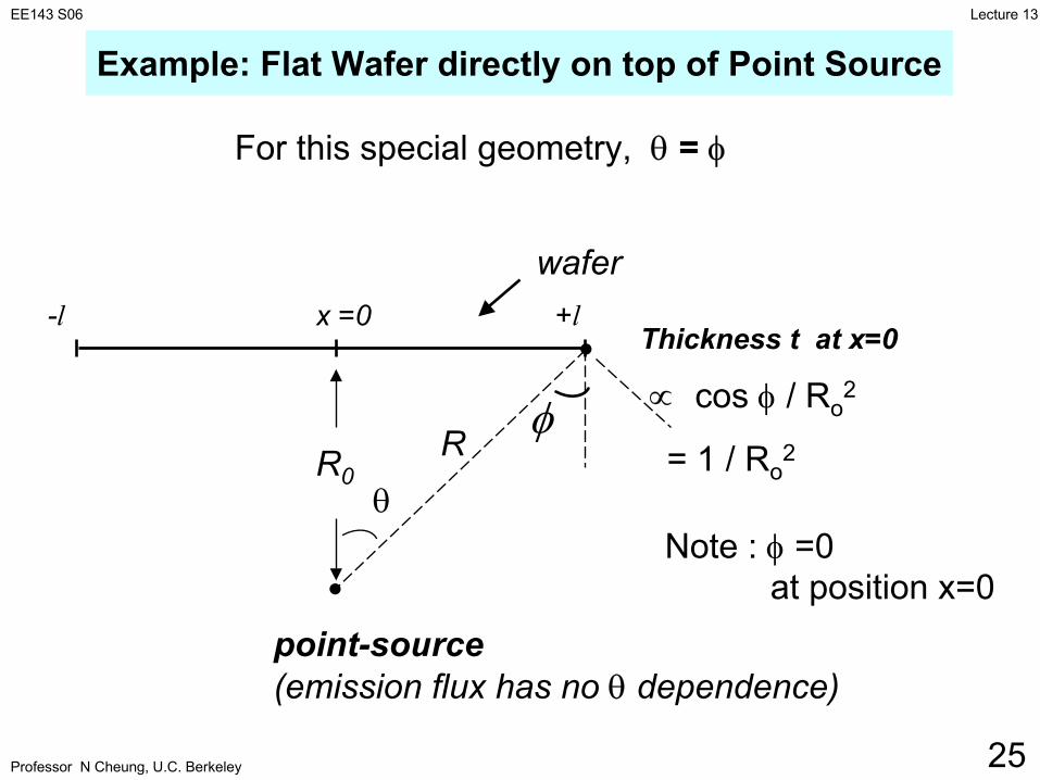
wafer-l +lx =0
R0R
point-source(emission flux has no θ dependence)
φ
Thickness t at x=0
∝ cos φ / Ro2
= 1 / Ro2
Note : φ =0 at position x=0
For this special geometry, θ = φ
θ
Example: Flat Wafer directly on top of Point Source
Professor N Cheung, U.C. Berkeley
Lecture 13EE143 S06
26
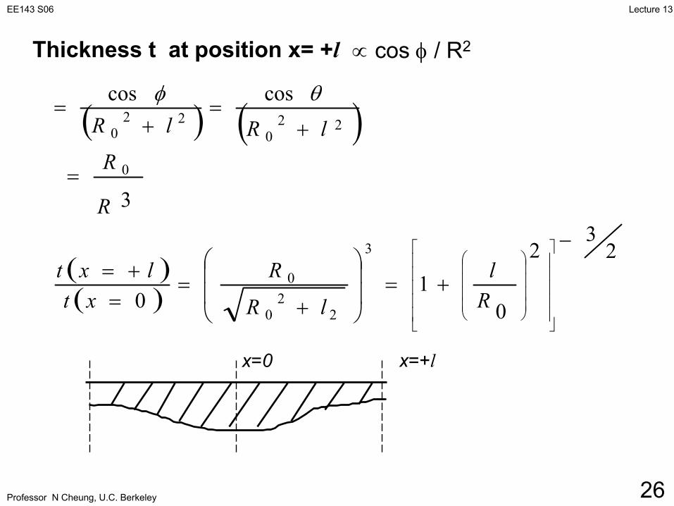
( ) ( )
( )( )
23
2
01
0
3
coscos
3
22
0
0
0
220
220
−
+=
+=
=+=
=
+=
+=
Rl
lR
Rxt
lxt
R
RlRlR
θφ
x=0 x=+l
Thickness t at position x= +l ∝ cos φ / R2
Professor N Cheung, U.C. Berkeley
Lecture 13EE143 S06
27
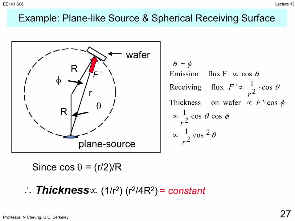
Example: Plane-like Source & Spherical Receiving Surface
θ
φθ
φ
θ
θφθ
2cos21
coscos21
cos'waferonThickness
cos21'fluxReceiving
cos flux F Emission
r
r
Fr
F
∝
∝
⋅∝
⋅∝
∝=
Since cos θ = (r/2)/R
Thickness∴ ∝ = constant(1/r2) (r2/4R2)
waferR
R
r
plane-source
θ
φ F ’
Professor N Cheung, U.C. Berkeley
Lecture 13EE143 S06
28
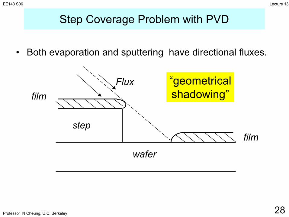
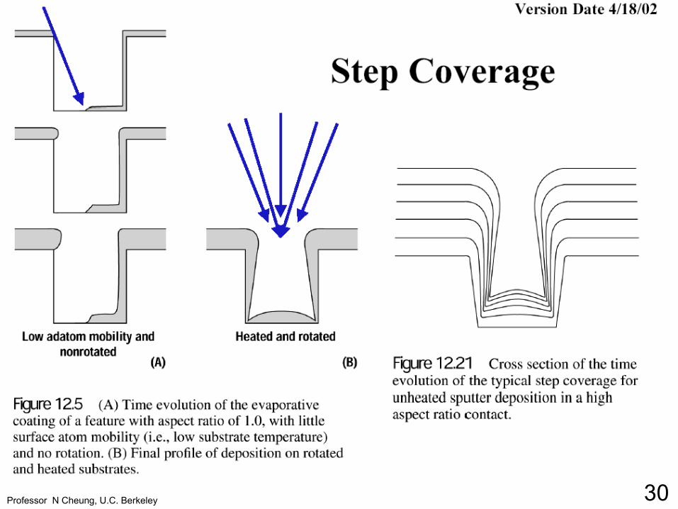
Step Coverage Problem with PVD
• Both evaporation and sputtering have directional fluxes.
wafer
step
filmFlux
film
“geometricalshadowing”
Professor N Cheung, U.C. Berkeley
Lecture 13EE143 S06
29
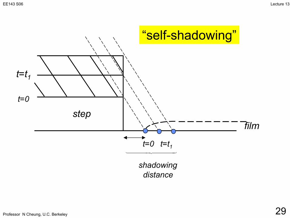
stepfilm
“self-shadowing”
t=t1
t=0 t=t11 244444 344444
shadowing distance
t=0
Professor N Cheung, U.C. Berkeley
Lecture 13EE143 S06
30
Professor N Cheung, U.C. Berkeley
Lecture 13EE143 S06
31
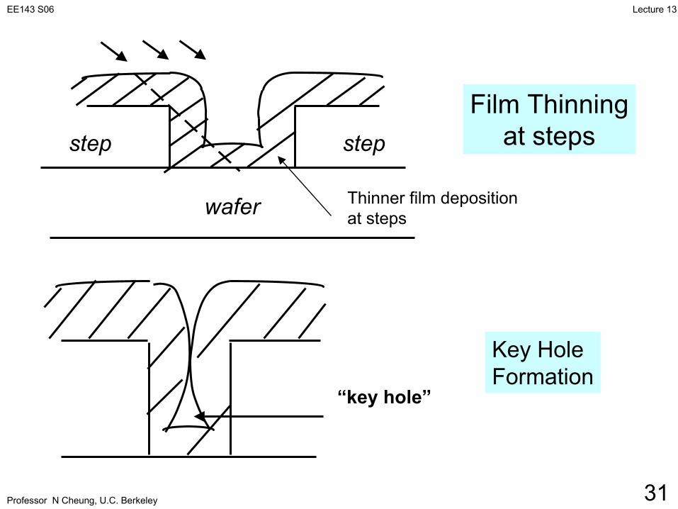
Film Thinningat stepsstep step
wafer
“key hole”
Key Hole Formation
Thinner film depositionat steps
Professor N Cheung, U.C. Berkeley
Lecture 13EE143 S06
32
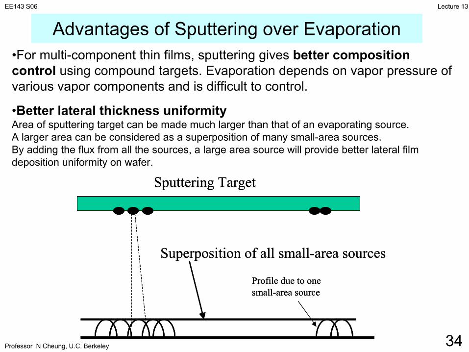
Sputtering Target
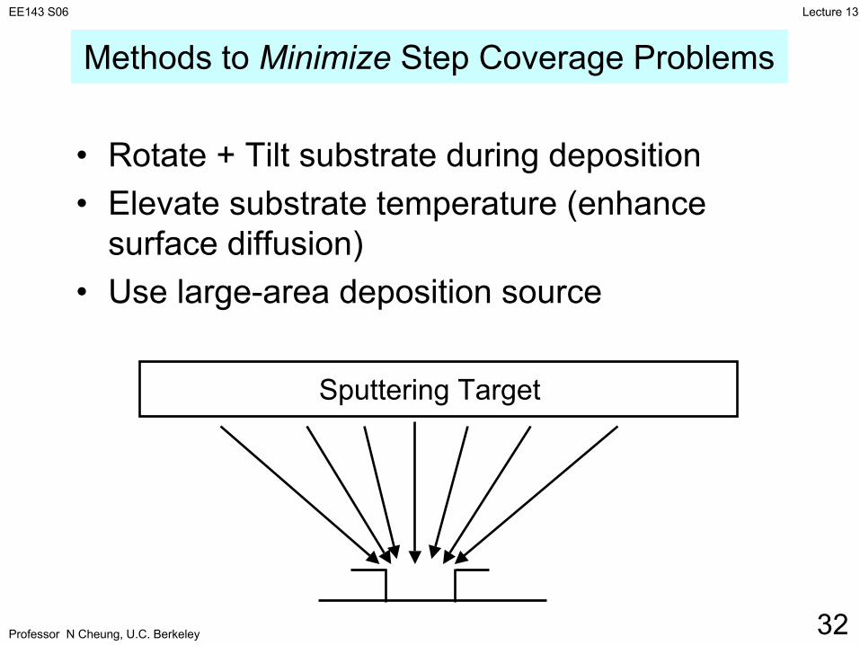
Methods to Minimize Step Coverage Problems
• Rotate + Tilt substrate during deposition• Elevate substrate temperature (enhance
surface diffusion)• Use large-area deposition source
Professor N Cheung, U.C. Berkeley
Lecture 13EE143 S06
33
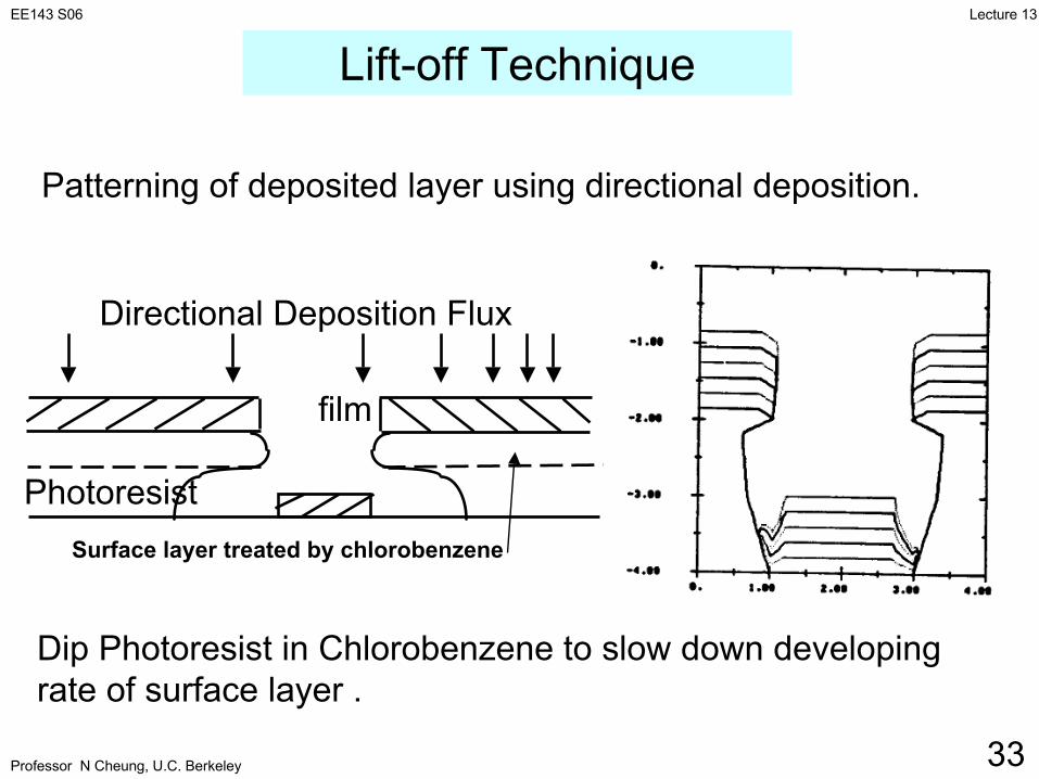
Dip Photoresist in Chlorobenzene to slow down developingrate of surface layer .
Surface layer treated by chlorobenzene
Photoresist
Directional Deposition Flux
film
Patterning of deposited layer using directional deposition.
Lift-off Technique
Professor N Cheung, U.C. Berkeley
Lecture 13EE143 S06
34
Sputtering Target
Profile due to one small-area source
Superposition of all small-area sources
Sputtering Target
Profile due to one small-area source
Superposition of all small-area sources
•Better lateral thickness uniformityArea of sputtering target can be made much larger than that of an evaporating source. A larger area can be considered as a superposition of many small-area sources. By adding the flux from all the sources, a large area source will provide better lateral film deposition uniformity on wafer.
•For multi-component thin films, sputtering gives better composition control using compound targets. Evaporation depends on vapor pressure of various vapor components and is difficult to control.
Advantages of Sputtering over Evaporation