Embed Size (px)
Citation preview

1
Analog to Digital Conversion
Using ATMEL’s ATmega168
2
ATmega168 PinsPDIP
PC5
PC4
PC3
PC2
PC1
PC0
GND
AREF
AVCC
PB5
PB4
PB3
PB2
PB1
PC6
PD0
PD1
PD2
PD3
PD4
VCC
GND
PB6
PB7
PD5
PD6
PD7
PB0
1
2
3
4
5
6
7
8
9
10
11
12
13
14
28
27
26
25
24
23
22
21
20
19
18
17
16
15
(ADC5/SCL/PCINT13)
(ADC4/SDA/PCINT12)
(ADC3/PCINT11)
(ADC2/PCINT10)
(ADC1/PCINT9)
(ADC0/PCINT8)
(SCK/PCINT5)
(MISO/PCINT4)
(MOSI/OC2A/PCINT3)
(OC1A/PCINT1)(SS/OC1B/PCINT2)
(PCINT16/RXT)
(PCINT17/TXD)
(PCINT18/INT0)
(PCINT19/OC2B/INT1)
(PCINT20/XCK/T0)
(PCINT6/XTAL1/TOSC1
(PCINT7/XTAL2/TOSC2
(PCINT21/OC0B/T1)
(PCINT23/AIN1)
PCINT0/CLK0/ICP1)
(PCINT22/OC0A/AIN0)
(PCINT14/RESET)
Caveat: If using ADC0-3, do not use any other of these pins as a Digital Output (Noise). If using ADC4-5, do not use the other pin as a Digital Output.
3
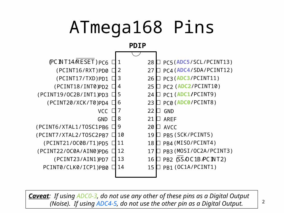
ADC Multiplexer
Key Registers to enable ADC
1. ADMUX – ADC Multiplexer Selection Register
2. ADCSRA – ADC Control and Status Register A
3. ADCSRB – ADC Control and Status Register B
4. DIDR0 – Digital Input Disable Register 0
4
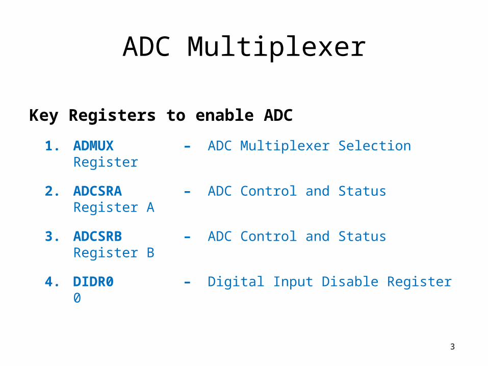
1. ADMUX – ADC Multiplexer Selection Register
Bit 7 6 5 4 3 2 1 0
0x7C REFS1 REFS0 ADLAR - MUX3 MUX2 MUX1 MUX0
Read/Write R/W R/W R/W R/W R/W R/W R/W R/W
Initial Value 0 0 0 0 0 0 0 0
• Bit 7:6 – REFS1:0: Reference Selection BitsThese bits select the voltage reference for the ADC, as shown below. If these bits are changed during a conversion, the change will not go in effect until this conversion is complete (ADIF in ADCSRA is set). The internal voltage reference options may not be used if an external reference voltage is being applied to the AREF pin.
Voltage Reference Selections for ADC
REFS1 REFS0 Voltage Reference Selection0 0 AREF, Internal Vref turned off0 1 AVCC with external capacitor at AREF pin1 0 Reserved1 1 Internal 1.1V Voltage Reference with external capacitor at AREF pin
5
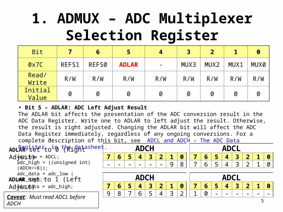
1. ADMUX – ADC Multiplexer Selection Register
Bit 7 6 5 4 3 2 1 0
0x7C REFS1 REFS0 ADLAR - MUX3 MUX2 MUX1 MUX0
Read/Write R/W R/W R/W R/W R/W R/W R/W R/W
Initial Value 0 0 0 0 0 0 0 0
• Bit 5 – ADLAR: ADC Left Adjust ResultThe ADLAR bit affects the presentation of the ADC conversion result in the ADC Data Register. Write one to ADLAR to left adjust the result. Otherwise, the result is right adjusted. Changing the ADLAR bit will affect the ADC Data Register immediately, regardless of any ongoing conversions. For a complete description of this bit, see ”ADCL and ADCH – The ADC Data Register” in the datasheet.
ADCH7 6 5 4 3 2 1 0- - - - - - 9 8
ADCL7 6 5 4 3 2 1 07 6 5 4 3 2 1 0
ADCH7 6 5 4 3 2 1 09 8 7 6 5 4 3 2
ADCL7 6 5 4 3 2 1 01 0 - - - - - -
ADLAR set to 0 (Right Adjust)
ADLAR set to 1 (Left Adjust)adc_data = adc_high;
adc_low = ADCL; adc_high = ((unsigned int) (ADCH<<8));adc_data = adc_low | adc_high;
Caveat: Must read ADCL before ADCH
6
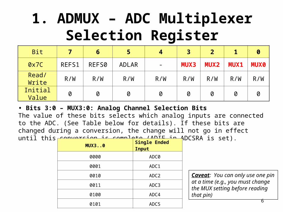
1. ADMUX – ADC Multiplexer Selection Register
Bit 7 6 5 4 3 2 1 0
0x7C REFS1 REFS0 ADLAR - MUX3 MUX2 MUX1 MUX0
Read/Write R/W R/W R/W R/W R/W R/W R/W R/W
Initial Value 0 0 0 0 0 0 0 0
• Bits 3:0 – MUX3:0: Analog Channel Selection BitsThe value of these bits selects which analog inputs are connected to the ADC. (See Table below for details). If these bits are changed during a conversion, the change will not go in effect until this conversion is complete (ADIF in ADCSRA is set).
MUX3..0 Single Ended Input
0000 ADC0
0001 ADC1
0010 ADC2
0011 ADC3
0100 ADC4
0101 ADC5
Caveat: You can only use one pin at a time (e.g., you must change the MUX setting before reading that pin)
7
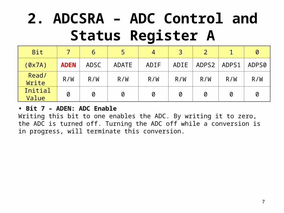
2. ADCSRA – ADC Control and Status Register A
Bit 7 6 5 4 3 2 1 0
(0x7A) ADEN ADSC ADATE ADIF ADIE ADPS2 ADPS1 ADPS0
Read/Write R/W R/W R/W R/W R/W R/W R/W R/W
Initial Value 0 0 0 0 0 0 0 0
• Bit 7 – ADEN: ADC EnableWriting this bit to one enables the ADC. By writing it to zero, the ADC is turned off. Turning the ADC off while a conversion is in progress, will terminate this conversion.
8
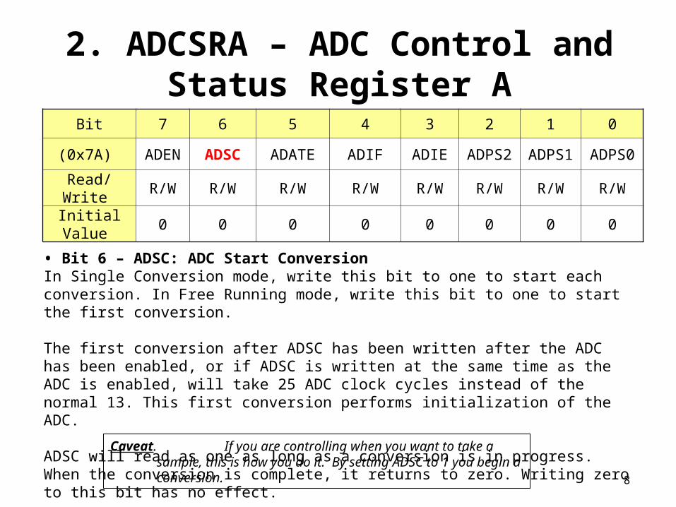
2. ADCSRA – ADC Control and Status Register A
Bit 7 6 5 4 3 2 1 0
(0x7A) ADEN ADSC ADATE ADIF ADIE ADPS2 ADPS1 ADPS0
Read/Write R/W R/W R/W R/W R/W R/W R/W R/W
Initial Value 0 0 0 0 0 0 0 0
• Bit 6 – ADSC: ADC Start ConversionIn Single Conversion mode, write this bit to one to start each conversion. In Free Running mode, write this bit to one to start the first conversion.
The first conversion after ADSC has been written after the ADC has been enabled, or if ADSC is written at the same time as the ADC is enabled, will take 25 ADC clock cycles instead of the normal 13. This first conversion performs initialization of the ADC.
ADSC will read as one as long as a conversion is in progress. When the conversion is complete, it returns to zero. Writing zero to this bit has no effect.
Caveat. If you are controlling when you want to take a sample, this is how you do it. By setting ADSC to 1 you begin a conversion.

9
2. ADCSRA – ADC Control and Status Register A
Bit 7 6 5 4 3 2 1 0
(0x7A) ADEN ADSC ADATE ADIF ADIE ADPS2 ADPS1 ADPS0
Read/Write R/W R/W R/W R/W R/W R/W R/W R/W
Initial Value 0 0 0 0 0 0 0 0
• Bit 5 – ADATE: ADC Auto Trigger EnableWhen this bit is written to one, Auto Triggering of the ADC is enabled. The ADC will start a conversion on a positive edge of the selected trigger signal. The trigger source is selected by setting the ADC Trigger Select bits, ADTS in ADCSRB.
10
2. ADCSRA – ADC Control and Status Register A
Bit 7 6 5 4 3 2 1 0
(0x7A) ADEN ADSC ADATE ADIF ADIE ADPS2 ADPS1 ADPS0
Read/Write R/W R/W R/W R/W R/W R/W R/W R/W
Initial Value 0 0 0 0 0 0 0 0
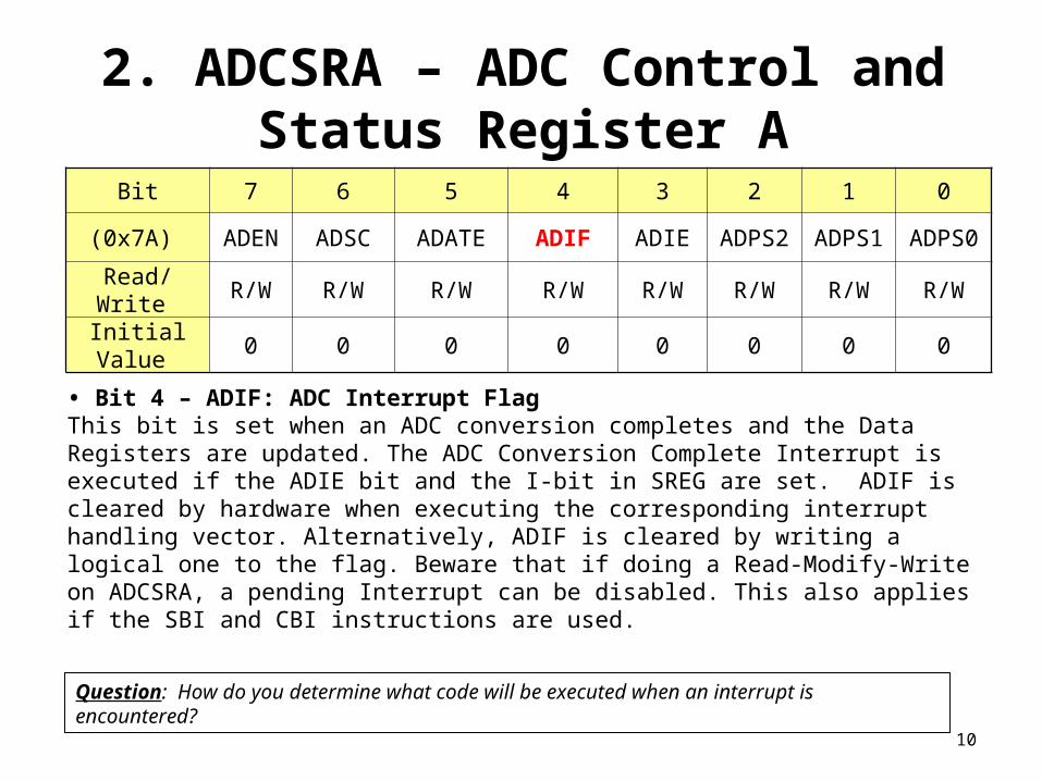
• Bit 4 – ADIF: ADC Interrupt FlagThis bit is set when an ADC conversion completes and the Data Registers are updated. The ADC Conversion Complete Interrupt is executed if the ADIE bit and the I-bit in SREG are set. ADIF is cleared by hardware when executing the corresponding interrupt handling vector. Alternatively, ADIF is cleared by writing a logical one to the flag. Beware that if doing a Read-Modify-Write on ADCSRA, a pending Interrupt can be disabled. This also applies if the SBI and CBI instructions are used.
Question: How do you determine what code will be executed when an interrupt is encountered?
11
2. ADCSRA – ADC Control and Status Register A
Bit 7 6 5 4 3 2 1 0
(0x7A) ADEN ADSC ADATE ADIF ADIE ADPS2 ADPS1 ADPS0
Read/Write R/W R/W R/W R/W R/W R/W R/W R/W
Initial Value 0 0 0 0 0 0 0 0
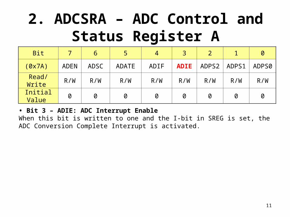
• Bit 3 – ADIE: ADC Interrupt EnableWhen this bit is written to one and the I-bit in SREG is set, the ADC Conversion Complete Interrupt is activated.
12
2. ADCSRA – ADC Control and Status Register A
Bit 7 6 5 4 3 2 1 0
(0x7A) ADEN ADSC ADATE ADIF ADIE ADPS2 ADPS1 ADPS0
Read/Write R/W R/W R/W R/W R/W R/W R/W R/W
Initial Value 0 0 0 0 0 0 0 0
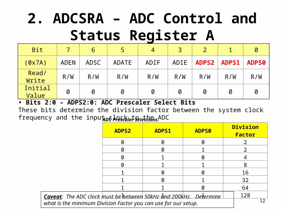
• Bits 2:0 – ADPS2:0: ADC Prescaler Select BitsThese bits determine the division factor between the system clock frequency and the input clock to the ADC
ADPS2 ADPS1 ADPS0 Division Factor0 0 0 20 0 1 20 1 0 40 1 1 81 0 0 161 0 1 321 1 0 641 1 1 128
ADC Prescaler Selections:
Caveat: The ADC clock must be between 50kHz and 200kHz. Determine what is the minimum Division Factor you can use for our setup.
13
3. ADCSRB – ADC Control and Status Register B
Bit 7 6 5 4 3 2 1 0
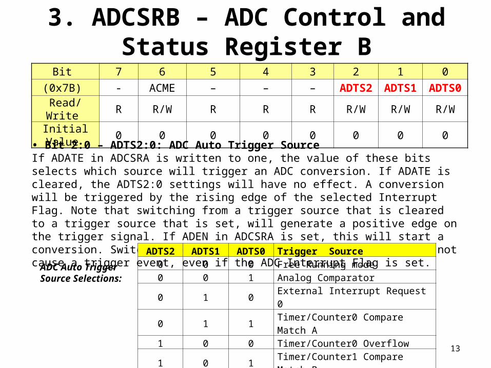
(0x7B) - ACME – – – ADTS2 ADTS1 ADTS0
Read/Write R R/W R R R R/W R/W R/W
Initial Value 0 0 0 0 0 0 0 0
• Bit 2:0 – ADTS2:0: ADC Auto Trigger SourceIf ADATE in ADCSRA is written to one, the value of these bits selects which source will trigger an ADC conversion. If ADATE is cleared, the ADTS2:0 settings will have no effect. A conversion will be triggered by the rising edge of the selected Interrupt Flag. Note that switching from a trigger source that is cleared to a trigger source that is set, will generate a positive edge on the trigger signal. If ADEN in ADCSRA is set, this will start a conversion. Switching to Free Running mode (ADTS[2:0]=0) will not cause a trigger event, even if the ADC Interrupt Flag is set.
ADTS2 ADTS1 ADTS0 Trigger Source0 0 0 Free Running mode0 0 1 Analog Comparator0 1 0 External Interrupt Request 00 1 1 Timer/Counter0 Compare Match A1 0 0 Timer/Counter0 Overflow1 0 1 Timer/Counter1 Compare Match B1 1 0 Timer/Counter1 Overflow1 1 1 Timer/Counter1 Capture Event
ADC Auto Trigger Source Selections:
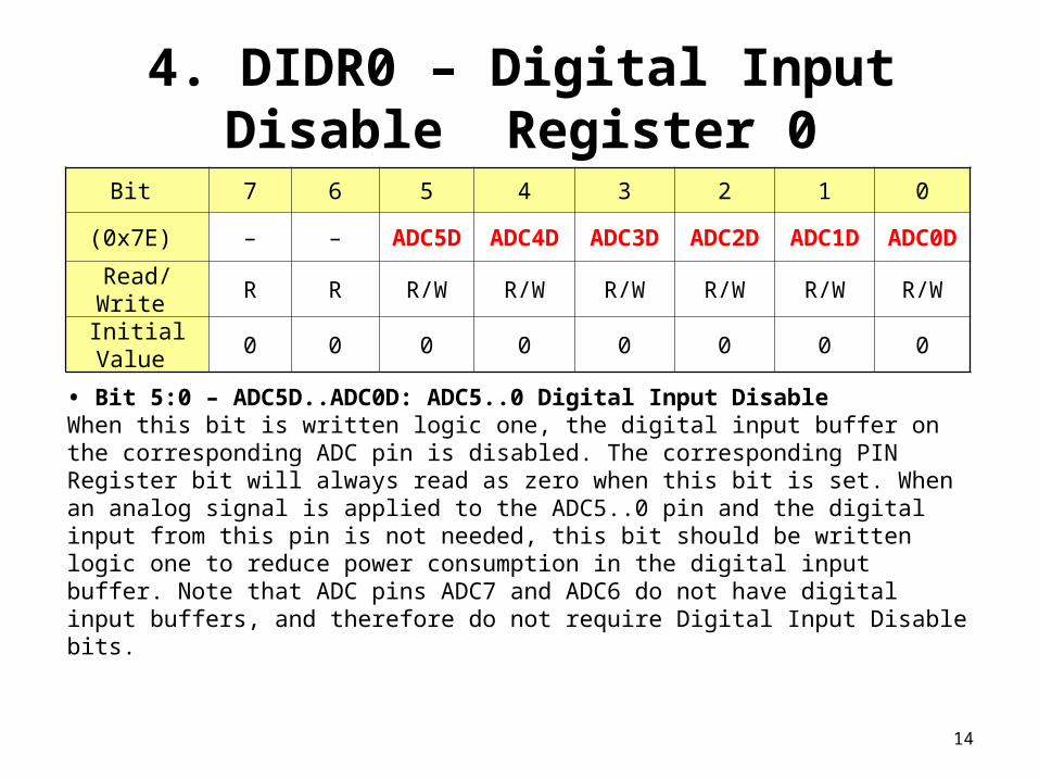
14
4. DIDR0 – Digital Input Disable Register 0
Bit 7 6 5 4 3 2 1 0
(0x7E) – – ADC5D ADC4D ADC3D ADC2D ADC1D ADC0D
Read/Write R R R/W R/W R/W R/W R/W R/W
Initial Value 0 0 0 0 0 0 0 0
• Bit 5:0 – ADC5D..ADC0D: ADC5..0 Digital Input DisableWhen this bit is written logic one, the digital input buffer on the corresponding ADC pin is disabled. The corresponding PIN Register bit will always read as zero when this bit is set. When an analog signal is applied to the ADC5..0 pin and the digital input from this pin is not needed, this bit should be written logic one to reduce power consumption in the digital input buffer. Note that ADC pins ADC7 and ADC6 do not have digital input buffers, and therefore do not require Digital Input Disable bits.

15
Lab 3 – Search LabWiring Diagram
1 2 3 4 5 6 7 8 9 10 11 12 13 14
28 27 26 25 24 23 22 21 20 19 18 17 16 15
PC6PD0
PD1PD2
PD3PD4
VccGND
PB6PB7
PD5PD6
PD7PB0
PC5PC4
PC3PC2
PC1PC0
GNDAREF
AVccPB5
PB4PB3
PB2PB1
ATMega 168
Vcc
Vcc
C1
100nF
Vsensor
CdS CdS