Embed Size (px)
Citation preview

1
4 Bit Arithmetic Logic Unit
Adithya V KodatiHayagreev Pattabhiraman
Vemuri KoneswaraAdvisor: Dave Parent
12/4/2005

2
Abstract
• Designed a fully functional 4-bit ALU using Philips 74HC/HCT181 schematic.
• Frequency of operation: 250Mhz
• Power dissipated : 24.96 mW
• Area : 676x513uM2
• D-flip flops were used to connect the inputs and outputs

3
Introduction• The ALU is the basic building block of most
digital circuits. Hence having a proper understanding and knowledge of how it should be designed and functions is necessary for a design engineer.
• Using CMOS design to implement the functions helps one to understand the design flow as well as adept use of Cadence software.
• This project also builds a strong foundation for other advanced design courses which use different processes to implement functionality.

4
Project Details
• Performs full carry look-ahead for arithmetic operation.
• 16 arithmetic and 16 logical operations
• Works with active high as well as active low inputs
• All inputs and outputs are connected via D-flip flops.

5
Table of functions
Courtesy PHILIPS SEMICONDUCTOR

6
Schematic and longest path

7
Longest path transistor sizing
CELL CintCg or Cin of load Cg+Cint phl CJN WN WP
F F s F/cm^2 cm cm
AND4 NOR2 5.00E-15 2.0000E-14 2.5000E-14 2.50E-10 4.23E-08 2.30E-04 4.72E-04
NAND2 5.00E-15 1.1786E-14 1.6786E-14 2.00E-10 4.23E-08 3.03E-04 2.70E-04
XOR XOR 5.00E-15 9.6185E-15 1.4619E-14 4.00E-10 4.23E-08 3.58E-04 6.20E-04
INV 5.00E-15 1.6424E-14 2.1424E-14 1.30E-10 4.23E-08 1.70E-04 3.06E-04
NOR4 INV 5.00E-15 8.0038E-15 1.3004E-14 1.00E-10 4.23E-08 2.18E-04 2.87E-04
NAND2 5.00E-15 8.4750E-15 1.3475E-14 2.35E-10 4.23E-08 1.71E-04 1.88E-04
NOR2 5.00E-15 6.0298E-15 1.1030E-14 2.00E-10 4.23E-08 9.13E-04 9.39E-04
AND5 NOR2 5.00E-15 3.1075E-14 3.6075E-14 3.00E-10 4.23E-08 2.20E-04 4.40E-04
NAND3 5.00E-15 1.1073E-14 1.6073E-14 2.60E-10 4.23E-08 8.19E-04 4.82E-04
NOR2 NOR2 5.00E-15 2.1823E-14 2.6823E-14 2.35E-10 4.23E-08 2.65E-04 5.71E-04
AND3 INV 5.00E-15 1.4023E-14 1.9023E-14 1.30E-10 4.23E-08 2.05E-04 2.75E-04
NAND3 5.00E-15 8.0554E-15 1.3055E-14 3.00E-10 4.23E-08 4.21E-04 2.46E-04
INV INV 5.00E-15 1.1189E-14 1.6189E-14 8.00E-11 4.23E-08 2.71E-04 4.91E-04

8
SCHEMATIC

9
LAYOUT

10
LAYOUT VERSUS SCHEMATIC(LVS)

11
LVS Report

12
LVS report contd..

13
Simulations
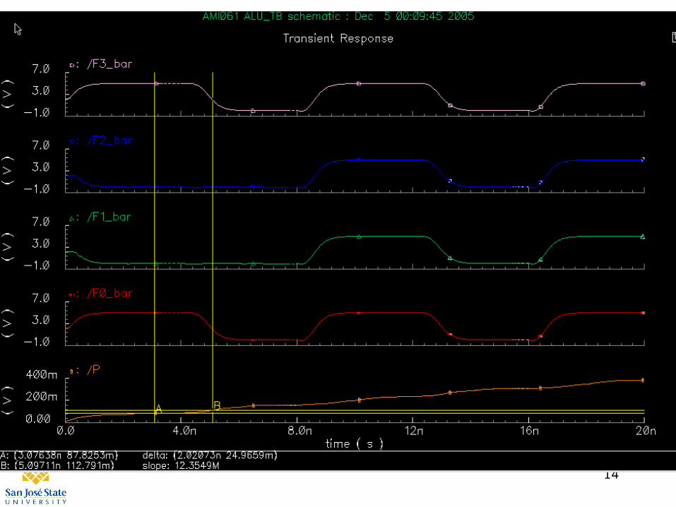
14

15
Important lessons learnt• Divide the circuit into cells. Perform DRC
and LVS at each stage.
• Confine usage of metal3 to the later stages of layout.
• Design floor plan and routing of major signals before you start the overall layout.
• Use Cadence lab to the maximum extent.

16
Acknowledgements • Professor Parent
• Thanks to Labtam’s Xlitepro for the remote login.
• Thanks to Cadence Design Systems for the VLSI lab.