Embed Size (px)
Citation preview
1
4-bit ALU
Cailan ShenTing-Lu Yang
Advisor: Dr. ParentMay 11, 2005

2
Agenda
• Introduction• Project (Experimental) Details
– ALU design in Cadence– DFF, MUX and Adder
• Summary– Project result– Lesson learned

3
Introduction• The 4-bit ALU that our group designed can
perform following functions:– Add, Subtract, NOR, OR, and AND.
• The 4-bit ALU operates at 200 MHz with an area of 300 um x 320 um and use 1.3 mW power.
• The 4-bit ALU is made up of 4 identical 1-bit ALU, and DFFs ensure the 4-bit ALU to obtain the correct inputs and send out correct outputs.
• This project is worthwhile because this ALU has all the logic blocks that we learned in class.

4
Project Description and ALU Schematic
- 1-bit Adder- Four 2 to 1 MUXs- 1 AND and 1 OR gates- Four control inputs, two
data inputs.
1 B A B -A
B and A Bnor A

5
Longest Path Calculations
• Note: All widths are in microns and capacitances in fF
nsns
PHL 313.16
5
6
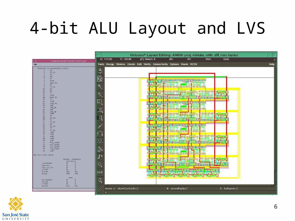
4-bit ALU Layout and LVS

7
SimulationALU Control Lines Function
A_inv B_inv OP1 OP0
0 0 0 0 AND
0 0 0 1 OR
0 0 1 0 ADD
0 1 1 0 SUBTRACT
1 1 0 0 NOR
Inputs
A B
1010 1010
1010 1011
A – B = 1010 -1011 =1111Cout = 0 (Borrowed)

8
Verification of Final Output

9
Power = 1.3 mW

10
Summary
• After this project, we became familiar with Cadence tool and the fundamental concepts of IC design.
• The total area is = 300um x 320um• The power = 1.3mW• Lessons learned
• How to fix the LVS error• Learn how to work in a team• Learn how to make trade offs

11
Acknowledgements
• Thanks to Cadence Design Systems for the VLSI lab
• Thanks to Synopsys for Software donation.
• Thanks to Professor David Parent.