Embed Size (px)
Citation preview

AN-186 - Layout Design Guidelines for PD69108 PoE Systems Company Confidential
Introduction________________ This application note provides detailed information and PCB design guidelines for the implementation of a 48-port Power over Ethernet (PoE) system, based on Microsemi’s™ 8-channel PoE Manager, the PD69108. Using this application note, the PCB designer can integrate PoE capabilities into an Ethernet switch.
The PD69108 device is an 8 port, mixed-signal, high-voltage PoE driver. It enables detection of IEEE802.3at-2009 compliant Type 1 and Type 2 PDs (Powered Devices), ensuring safe power feeding and disconnection of ports with full digital control and a minimum of external components. The PD69108 is designed to implement all real time functions as specified in the IEEE 802.3af and IEEE802.3at standard including detection, classification and port status monitoring, as well as system level activities such as: power management and MIB support for system management. The PD69108 is designed to detect and disable disconnected ports, using DC disconnection methods only.
This application note is to be used in conjunction with application note AN-185, Catalogue Number 06-0080-080.
Applicable Documents_______ IEEE 802.3af-2003 standard, DTE Power
via MDI IEEE802.3at-2009 Standard, DTE Power
via MDI PD69108 Data Sheet, Catalogue Number
06-0057-058 PD69100 Data Sheet, Catalogue Number
06-0069-058 Microsemi Application Note AN-185 for
Designing a 48-port Enhanced PoE System
Isolation and Termination____ According to the IEEE 802.3af and the IEEE802.3at standard, certain isolation requirements need to be met in all PoE equipment. In addition, EMI limitations should be considered, as specified in the FCC and European EN regulations.
These requirements are taken into account by PoE switch vendors, while designing the switch circuitry. However, when a PoE Manager is integrated into a switch, special design considerations must be met,
due to the unique combination of data and power circuitries.
The following paragraphs define these requirements and provide recommendations for their implementation, so as to assist designers in meeting those requirements and in integrating the Microsemi’s PoE Chip Set and the daughter boards.
Isolation As specified in the IEEE PoE standards, 1500 Vac rms isolation is required between the switch’s main board circuitry including protective and frame ground and the Media Dependent Interface (MDI). Figure 1 illustrates the overall isolation requirements.
Figure 1: Isolation Requirements Scheme Meeting Requirements
High Voltage Isolation For a switch with no PoE circuitry: isolation
requirements between the physical inputs and the data connectors are met by using an isolated AC/DC power supply and isolated pulse transformers (see Figure 2).
When integrating a PoE circuitry into a switch, the output power can be supplied through the central tap of the pulse transformer’s secondary side (unless power is provided over the spare pairs). This connectivity can bypass the pulse transformer’s isolation, if the PoE ground or DC input is connected to the switch’s circuitry/ground.
AN-186 - Layout Design Guidelines for PD69108 PoE Systems Company Confidential
Copyright © 2010 Microsemi Page 2 Rev. 0.2 / 10-Apr-11 Analog Mixed Signal Group
2381 Morse Avenue, Irvine, CA 92614, USA; Within the USA: (800) 713-4113, Outside the USA: (949) 221-7100 Fax: (949) 756-0308
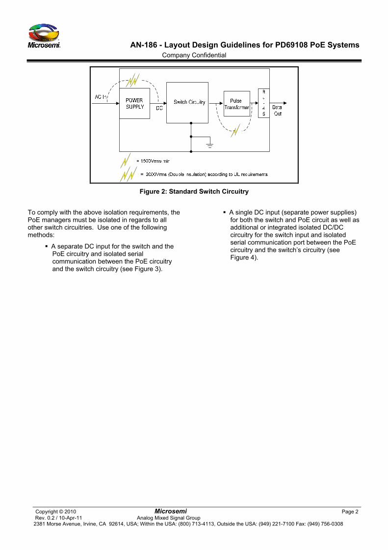
Figure 2: Standard Switch Circuitry
To comply with the above isolation requirements, the PoE managers must be isolated in regards to all other switch circuitries. Use one of the following methods:
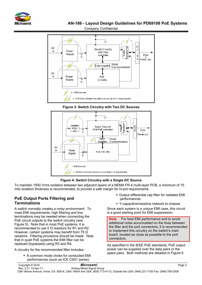
A separate DC input for the switch and the PoE circuitry and isolated serial communication between the PoE circuitry and the switch circuitry (see Figure 3).
A single DC input (separate power supplies) for both the switch and PoE circuit as well as additional or integrated isolated DC/DC circuitry for the switch input and isolated serial communication port between the PoE circuitry and the switch’s circuitry (see Figure 4).
AN-186 - Layout Design Guidelines for PD69108 PoE Systems Company Confidential
Copyright © 2010 Microsemi Page 3 Rev. 0.2 / 10-Apr-11 Analog Mixed Signal Group
2381 Morse Avenue, Irvine, CA 92614, USA; Within the USA: (800) 713-4113, Outside the USA: (949) 221-7100 Fax: (949) 756-0308
Figure 3: Switch Circuitry with Two DC Sources
Figure 4: Switch Circuitry with a Single DC Source
To maintain 1500 Vrms isolation between two adjacent layers of a NEMA FR-4 multi-layer PCB, a minimum of 15 mils isolation thickness is recommended, to provide a safe margin for hi-pot requirements.
PoE Output Ports Filtering and Terminations
A switch normally creates a noisy environment. To meet EMI requirements, high filtering and line terminations may be needed when connecting the PoE circuit outputs to the switch circuitry (see Figure 5). Note that in most PoE systems, it is recommended to use 0 Ω resistors for R1 and R2. However, certain systems may benefit from 75 Ω resistors. Filtering provisions should be made. Note that in quiet PoE systems the EMI filter can be replaced (bypassed) using R3 and R4.
A circuitry for the recommended filter includes:
A common mode choke for conducted EMI performances (such as ICE CS01 series)
Output differential cap filter for radiated EMI performances
Y-capacitive/resistive network to chassis
Since each system is a unique EMI case, this circuit is a good starting point for EMI suppression.
Note For best EMI performance and to avoid additional noise accumulated on the lines between the filter and the port connectors, it is recommended to implement this circuitry on the switch’s main board, located as close as possible to the port connectors.
As specified in the IEEE PoE standards, PoE output power can be supplied over the data pairs or the spare pairs. Both methods are detailed in Figure 6

AN-186 - Layout Design Guidelines for PD69108 PoE Systems Company Confidential
Copyright © 2010 Microsemi Page 4 Rev. 0.2 / 10-Apr-11 Analog Mixed Signal Group
2381 Morse Avenue, Irvine, CA 92614, USA; Within the USA: (800) 713-4113, Outside the USA: (949) 221-7100 Fax: (949) 756-0308
which illustrates an MDI-X (or Auto MDI-X) connection associated with the switch.
Isolating the Stacked Modular Jack Assembly The IEEE PoE standards require 1500 Vrms isolation between PoE voltages and frame ground (EGND). Notice that RJ-45 jack assemblies have a metal cover that 80 mils almost reaches to the PCB surface.
Maintain a 80 mils traces clearance between EGND traces for the RJ-45 modular jack assembly metal covering and adjacent circuit paths and components. To prevent 1500 Vrms isolation violation, it is necessary to provide layout clearances of PoE traces on the top layer, in the vicinity of the RJ-45 connector assemblies.
PoE technology involves voltages as high as 57 VDC. Thus, plan adjacent traces for 100 VDC
operational creepage. Operational creepage should be maintained to prevent breakdown between traces carrying these potentials.
Figure 5: Recommended EMI Filter
IN )+(
IN )-(
R J 4 5
T 1
T 1
R J 4 5
1236
1236
4578
E M IF IL T E R
P o EC IR C U IT R Y
E M IF IL T E R
P o EC IR C U I T R Y
P o w e r fe e d in g o v e r d a ta p a ir s ( 1 ,2 a n d 3 , 6 )
P o w e r fe e d in g o v e r s p a r e p a ir s ( 4 ,5 a n d 7 , 8 )
4578
)-(
)+(
)+(
)-(
P H Y
P H Y
IN )+(
IN )-(
R J 4 5
T 1 1236
P o w e r fe e d in g o v e r d a ta p a ir s ( 1 ,2 a n d 3 ,6 )
P o w e r fe e d in g o v e r d a ta p a ir s ( 4 , 5 , a n d 7 ,8 )
4578
)-(
)+(
P H Y
1 0 M b /s a n d 1 0 0 M b / s E t h e r n e t P H Y s 1 0 0 0 M b / s E t h e r n e t P H Y s
T 2
P H Y
E M IF IL T E R
P o EC IR C U IT R Y
IN )+(
IN )-(
R J 4 5
T 1 1236
4578
)-(
)+(
P H Y
T 2
P H Y
E M IF IL T E R
P o EC IR C U IT R Y
Figure 6: Output Ports Design Details
Layout Guidelines_________ Microsemi’s PD69108 PoE Manager is designed to simplify the integration of PoE-circuitry, based on the IEEE PoE standards, into switches. The pin-out arrangement has been configured for optimal PCB routing. Microsemi recommendations for proper PCB layout follow.
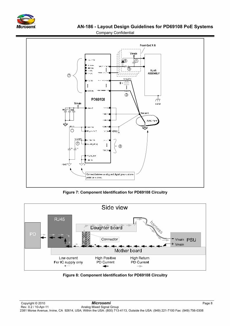
Figure 7 describes the various circuits and elements surrounding the PD69108 PoE Manager in the block diagram. This block diagram includes the following peripheral elements, identified by numbers:
5 V Voltage source (VAUX5) (1)
3.3 V Voltage source (VAUX3P3) (2)
Sense resistor for current measurement (3)
Output capacitor used for filtering (4)

AN-186 - Layout Design Guidelines for PD69108 PoE Systems Company Confidential
Copyright © 2010 Microsemi Page 5 Rev. 0.2 / 10-Apr-11 Analog Mixed Signal Group
2381 Morse Avenue, Irvine, CA 92614, USA; Within the USA: (800) 713-4113, Outside the USA: (949) 221-7100 Fax: (949) 756-0308
Protection Fuse (5)
Protection diode against reverse polarity (6)
RESET, ESPI Bus, ESPI Address Lines (7)
Power Good Inputs (8)
Note The VAUX5 supply may include an external transistor connected to pin 48, destined to increase current drive for external circuitry. To prevent heat from being transferred to the PD69108, place this transistor away from the PoE Managers.
For details on the interconnection circuitry of the PD69108, refer to the Application Notes listed in the "Applicable Documents" section.
The circuitry provided is intended to facilitate the design of a switch when integrating a PoE capability into it.
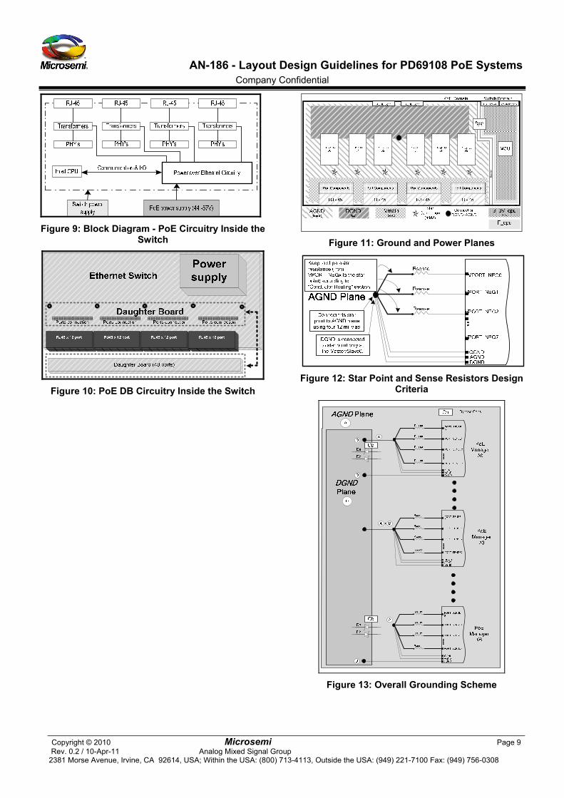
Locating PoE Circuitry in a Switch To minimize the length of high current traces, as well as RFI pick-up, place the PoE circuitry as close as possible to the switch’s pulse transformers. The circuit can be fully integrated into the switch’s PCB, or can be easily placed on top of the switch's using daughter board PoE application. Typical integration of PoE modules inside a switch is shown in Figure 9 and Figure 10
Ground and Power Planes Since the Chip Set PoE solution (PD69108 and PD69100) is a mixed-signal (analog and digital) circuitry, special care must be taken when routing the ground and power signals lines.
The reference design assumes a four layer board: top, mid1, mid2, bottom. The main planes are Vmain/AGND, DGND, 3_3V_cpu/F_cpu.
Ground planes are crucial for proper operation and should be designed in accordance with the following guidelines, as illustrated in Figure 11:
Separate analog and digital grounds, with a gap of at least 40 mils.
Analog ground plane (AGND) is utilized to transfer the heat generated by the PD69108 (see Thermal Pad Definition and Design). The AGND should be the bottom layer.
Earth ground is used to tie in the metal frame of the RJ-45 connectors. This ground is to be routed separately and connected to the switch’s metal chassis/enclosure
To prevent ground loop currents, use only a single connection point between the digital and analog grounds as shown in Figure 11 and Figure 13.
It is recommended that the grounding layout be implemented as described in Figure 10.
To minimize noise effects from the heavy currents flowing to the ports, a number of separate grounding areas are essential in the design. Establish several separate ground areas to concentrate sensitive circuits, apart from the main grounding surfaces.
Extend the A_cpu surface under pin 5 of the PoE Controller. This grounding area is part of and connected at one point (pin 5) to the floating (digital) ground (F_cpu). Connect the analog filtering capacitors to this ground.
To connect various DGND points and to enable stable impedance to the ESPI bus traces, extend the digital ground (DGND) surface under pins 35 - 48, 1, 2 of the PD69108 Managers.
Rsense resistors for each PoE Manager are all connected to local “star point”. The star center is connected to the analog ground (AGND) using four tied power via's of 12 mil diameter each (see Figure 12, Figure 13 and Figure 14.)
In addition the Rsense resistors’ “star point” connection for the PD69108 utilized as #0, is to be the focal interconnection point for the digital and analog grounds (see Figure 13)
Leave spacing for a ceramic 1 nF bypass capacitor near each PoE Manager (marked as “Cb” in Figure 13) between the analog and digital layers near each PoE Manager. The capacitors form low impedance paths for digital driving signals.
Leave appropriate spacing (provision for) for two parallel and inversed Schottky diodes (Da, Db) (Figure 13) between the analog and digital layers near each PoE Manager. The diodes form low impedance paths for highly energized signals running between analog and digital layers and enhance circuit immunity.
The power and return (ground) planes for the 48 V supply must be designed to carry 35 A continuous current, based on full 48-port capacity. Minimize DC power losses on this plane by using a wide copper land. When implementing the PoE circuitry on a daughter board, the hi current does not have to be routed through the daughter board but only the return path as can be note from Figure 8

AN-186 - Layout Design Guidelines for PD69108 PoE Systems Company Confidential
Copyright © 2010 Microsemi Page 6 Rev. 0.2 / 10-Apr-11 Analog Mixed Signal Group
2381 Morse Avenue, Irvine, CA 92614, USA; Within the USA: (800) 713-4113, Outside the USA: (949) 221-7100 Fax: (949) 756-0308
Current Flow Through the PoE application See Figure 8
The port's current flows in a DC disconnect application as follows:
1. Coming from the switch's power supply positive to the centertaps of the line transformer via a mother board wide trace (not through the DB)
2. From the centertap of the line transformer via the switch's RJ45 to the PD side
3. The return current from the PD flows via the RJ45 and the line transformer to the DB PoE circuitry.
4. From the DB analog ground (AGND) the current flows back to the switch's power supply negative via harness
Note The positive port's heavy current flows directly to the PD side without going through the PoE DB Managers.
Specific Component Placement________________
Peripheral Components To prevent heat transfer among various components, the following gaps should be maintained:.
Minimum gap between PD69108s should be 45 mm
Minimum gap between PD69108 to PoE controller should be 30 mm
Minimum gap between PD69108 to a boost transistor (if used) should be 30 mm. For further details refer to Application Note AN-185 for Designing a 48-port Enhanced PoE System. It is may be required to leave an open gap in the ground plane to isolate the heat transfer from the two areas
Do not group sense resistors together, to prevent a hot spot on the PCB, under full load conditions. It is recommend to leave at least 10 mm between the PD69108 and it's sense resistors.
PoE Controller and Peripherals Refer to the PD69100 Data Sheet, Catalogue Number 06-0069-058 for recommendations related to the PoE controller layout guidelines.
The following guidelines are destined for the integration of the PoE Controller into a PoE circuit.
Locate the filtering capacitors for VDD and for VDDA close to power and ground pins.
Termination resistors for the outgoing ESPI digital lines must be located close to the respective driving pins.
PD69108 PoE Manager and Peripherals The side of the PoE Manager that
includes pins 37 to 48 should face the digital ground (DGND plane.) The pins function as communication and control pins for the Manager (connect between the PoE Manager and the PoE controller via isolation circuitry)
Locate the bypass capacitors for the PoE Manager supply input close to the relevant pin. In cases where two bypass capacitors are placed on the same line, locate the lower value capacitor closer to the pin on the same layer and place the higher value capacitor at a more distant location.
Locate VAUX5 and VAUX3P3 0.1 µF and 4.7 µF filtering capacitors as close as possible to the PoE Manager pins 16 and 20 respectively.
Conductor Routing__________
General Guidelines Conductor (or printed lands) routing is to be performed as practiced in general layout guidelines, specifically:
Conductors that deliver a digital signal are to be routed between the analog and the digital ground planes.
Avoid routing analog signals above the digital ground.
The total resistance of all sense resistor traces (both sides) need to be 12 mOhm.
Specific Requirements for Clock and Sensitive Signals Issues that require special design considerations:
Each PD69108's port incorporates a current sense resistor. For proper power management and control, lay out these lines so that measured current is not impeded by adjacent ports current flow or by excessive path resistance. To do this, use a single common point to aggregate the current flow of all eight ports to the analog ground (AGND) layer. This point is referred to, as

AN-186 - Layout Design Guidelines for PD69108 PoE Systems Company Confidential
Copyright © 2010 Microsemi Page 7 Rev. 0.2 / 10-Apr-11 Analog Mixed Signal Group
2381 Morse Avenue, Irvine, CA 92614, USA; Within the USA: (800) 713-4113, Outside the USA: (949) 221-7100 Fax: (949) 756-0308
the local PoE Manager "star point" (see Figure 12, Figure 13 and Figure 14). It is critical to design the total layout path (traces resistance from PORT_SENSEx pin to the AGND star point) for an accurate resistance value, since a wrong resistance value results in current measurement error and unreliable power management. Parasitic resistance added by the layout traces must be 12 mOhms. Since routing requires narrow traces in some areas, wide traces in other areas are necessary to achieve total trace resistance of 12 mOhms.
The local “star point” need to carry high current from the sense resistors to AGND. To achieve this, use four tied power via's of 12 mil diameter each (See Figure 14). Avoid using plugged vias to preclude temperature rise
Route a senses trace (SENSE_NEG) from QGND (pin 21) to the local PoE Manager “star point”
The PD69108’s AGND (pins 7, 18, 30) must also be connected directly to the local PoE Manager “star point” by individual traces.
The IREF resistor (connects to pin 22), used for current reference, is directly connected to QGND (pin 21)
Carefully route the ESPI communication clock (SCK) line coming from the PoE Controller so that it will not disturb other lines. Two ground lines (connected to
DGND) could be routed alongside the clock line to isolate it from the rest of the lines.
Port Outputs For robust design, the ports output traces are to be 45-mil wide so as to handle maximum current and port power.
However to obtain a 10° C (maximum) copper rise, set the minimum width for traces in accordance with the layer location and copper thickness:
For two ounce copper, external layer: 15 mils
For two ounce copper, internal layer: 20 mils
For one ounce copper, external layer: 25 mils
For one ounce copper, internal layer: 30 mils
For 1/2 ounce copper, external layer: 30 mils
For 1/2 ounce copper, internal layer: 55 mils (20° C copper rise)
The ports output traces must be short and parallel to each other, to reduce RFI coupling and to keep the series resistance low.
The PoE ports outputs must be connected to the switch’s pulse transformers as shown in Figure 6. The common mode choke is used to reduce RFI noise. A ‘Bob-Smith’ termination (resistor-capacitor) to chassis ground is optional. The circuit is to be located as close as possible to the pulse transformer.
AN-186 - Layout Design Guidelines for PD69108 PoE Systems Company Confidential
Copyright © 2010 Microsemi Page 8 Rev. 0.2 / 10-Apr-11 Analog Mixed Signal Group
2381 Morse Avenue, Irvine, CA 92614, USA; Within the USA: (800) 713-4113, Outside the USA: (949) 221-7100 Fax: (949) 756-0308
Figure 7: Component Identification for PD69108 Circuitry
Figure 8: Component Identification for PD69108 Circuitry
AN-186 - Layout Design Guidelines for PD69108 PoE Systems Company Confidential
Copyright © 2010 Microsemi Page 9 Rev. 0.2 / 10-Apr-11 Analog Mixed Signal Group
2381 Morse Avenue, Irvine, CA 92614, USA; Within the USA: (800) 713-4113, Outside the USA: (949) 221-7100 Fax: (949) 756-0308
Figure 9: Block Diagram - PoE Circuitry Inside the Switch
Figure 10: PoE DB Circuitry Inside the Switch
Bar
rier
Figure 11: Ground and Power Planes
Figure 12: Star Point and Sense Resistors Design Criteria
Figure 13: Overall Grounding Scheme

AN-186 - Layout Design Guidelines for PD69108 PoE Systems Company Confidential
Copyright © 2010 Microsemi Page 10 Rev. 0.2 / 10-Apr-11 Analog Mixed Signal Group
2381 Morse Avenue, Irvine, CA 92614, USA; Within the USA: (800) 713-4113, Outside the USA: (949) 221-7100 Fax: (949) 756-0308
Figure 14: Star Point Layout
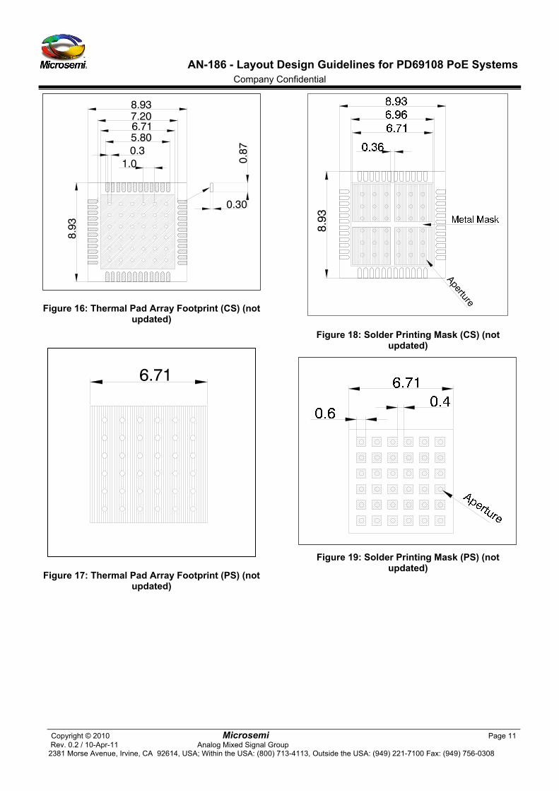
Thermal Pad Definition and Design___________________ The PD69108 utilizes a thermal dissipation exposed pad in a 48-pin 8 x 8 mm QFN package. The package is molded in such a way that the lead frame is exposed at the bottom surface of the package.
Direct soldering of the exposed pad to a copper land provides an efficient thermal path. In multilayer board designs, a matrix of 6x6 vias thermally connects the exposed pad to the copper planes.
Requirements The PCB design should consider the exposed pad of the PD69108. This pad is used for thermal cooling of the package. Basically, the PCB should be designed as shown in Figure 16 - Figure 19.
In these figures the PD69108 pad is soldered to a dedicated area on the PCB. This contact area is composed of a 36 vias array, each penetrating and thermally connecting to large ground areas in the PCB at various planes, providing efficient heat dissipation.
To ensure optimum thermal transfer through the thermal vias to internal planes or to the reverse side of the PCB, the vias system should not be used as used in web construction techniques. Web construction for PCB vias is a standard technique used to facilitate soldering, by designing the via to achieve high thermal resistance. This is not desirable for heat dissipation from the PD69108 package. It is recommended that vias used under the PD69108 package be internally connected to the planes, using continuous connection surrounding the whole diameter.
Thermal Pad Design The PD69108's exposed pad is a metal substrate on the bottom of the package. The attachment process for the exposed pad package is equivalent to standard surface mount packages.
Figure 15: Heat Dissipation in PC
See Figure 16 and Figure 17 (CS & PS) for a design layout of the recommended contact pad.
For proper heat dissipation, the following footprint / layout guidelines must be followed:
All thermal vias are to be connected to the AGND area under the PD69108
Via diameter should be approximately 0.3 mm with one ounce copper barrel plating. Solder flow into the vias from the component side can result in voids during the solder process and this must be avoided.
If copper plating does not plug the vias, apply stencil print solder paste onto the printed circuit side. This provides sufficient solder paste, filling those vias to avoid the above mentioned voids. Figure 18 and Figure 19 show the associated, solder printing masks (CS & PS). The solder mask openings are lined-up in respect to the 6 x 6 thermal via array. Since large solder printing mask openings may result in poor release, the opening should be subdivided as shown in these figures.
For a nominal package standoff of 0.1 mm, a solder mask stencil thickness of 5 mils should be considered.
AN-186 - Layout Design Guidelines for PD69108 PoE Systems Company Confidential
Copyright © 2010 Microsemi Page 11 Rev. 0.2 / 10-Apr-11 Analog Mixed Signal Group
2381 Morse Avenue, Irvine, CA 92614, USA; Within the USA: (800) 713-4113, Outside the USA: (949) 221-7100 Fax: (949) 756-0308
8.93
8.93
6.717.20
5.800.3
1.0 0.87
0.30
Figure 16: Thermal Pad Array Footprint (CS) (not updated)
6.71
Figure 17: Thermal Pad Array Footprint (PS) (not updated)
8.93
Aperture
Figure 18: Solder Printing Mask (CS) (not updated)
Figure 19: Solder Printing Mask (PS) (not updated)

AN-186 - Layout Design Guidelines for PD69108 PoE Systems Company Confidential
Copyright © 2010 Microsemi Page 12 Rev. 0.2 / 10-Apr-11 Analog Mixed Signal Group
2381 Morse Avenue, Irvine, CA 92614, USA; Within the USA: (800) 713-4113, Outside the USA: (949) 221-7100 Fax: (949) 756-0308
The information contained in the document (unless it is publicly available on the Web without access restrictions) is PROPRIETARY AND CONFIDENTIAL information of Microsemi and cannot be copied, published, uploaded, posted, transmitted, distributed or disclosed or used without the express duly signed written consent of Microsemi. If the recipient of this document has entered into a disclosure agreement with Microsemi, then the terms of such Agreement will also apply . This document and the information contained herein may not be modified, by any person other than authorized personnel of Microsemi. No license under any patent, copyright, trade secret or other intellectual property right is granted to or conferred upon you by disclosure or delivery of the information, either expressly, by implication, inducement, estoppels or otherwise. Any license under such intellectual property rights must be approved by Microsemi in writing signed by an officer of Microsemi.
Microsemi reserves the right to change the configuration, functionality and performance of its products at anytime without any notice. This product has been subject to limited testing and should not be used in conjunction with life-support or other mission-critical equipment or applications. Microsemi assumes no liability whatsoever, and Microsemi disclaims any express or implied warranty, relating to sale and/or use of Microsemi products including liability or warranties relating to fitness for a particular purpose, merchantability, or infringement of any patent, copyright or other intellectual property right. Any performance specifications believed to be reliable but are not verified and customer or user must conduct and complete all performance and other testing of this product as well as any user or customers final application. User or customer shall not rely on any data and performance specifications or parameters provided by Microsemi. It is the customer’s and user’s responsibility to independently determine suitability of any Microsemi product and to test and verify the same. The information contained herein is provided “AS IS, WHERE IS” and with all faults, and the entire risk associated with such information is entirely with the User. Microsemi specifically disclaims any liability of any kind including for consequential, incidental and punitive damages as well as lost profit. The product is subject to other terms and conditions which can be located on the web at http://www.microsemi.com/legal/tnc.asp
Revision History Revision Level / Date Para. Affected Description0.1 / 20 Apr. 10 Initial release
0.2 / 10 Apr. 11 Updates
© 2010 Microsemi Corp.
All rights reserved.
For support contact: [email protected] Catalogue Number: 06-0081-080
Visit our web site at: www.microsemi.com