Embed Size (px)
Citation preview
William Stallings
Computer Organization
and Architecture
8th Edition
Chapter 5
Internal Memory
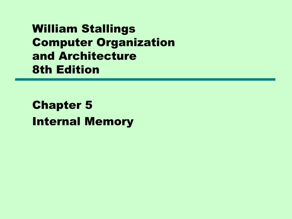
Semiconductor Memory Types
Memory Type Category Erasure Write Mechanism Volatility
Random-access
memory (RAM)Read-write memory Electrically, byte-level Electrically Volatile
Read-only
memory (ROM)
Read-only memory Not possible
Masks
Nonvolatile
Programmable
ROM (PROM)
Electrically
Erasable PROM
(EPROM)
Read-mostly memory
UV light, chip-level
Electrically Erasable
PROM (EEPROM)Electrically, byte-level
Flash memory Electrically, block-level

Semiconductor Memory
• RAM
—Misnamed as all semiconductor memory is random access
—Read/Write
—Volatile
—Temporary storage
—Static or dynamic

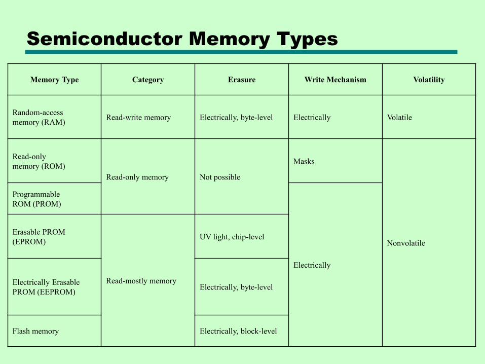
Memory Cell Operation

Dynamic RAM
• Bits stored as charge in capacitors
• Charges leak
• Need refreshing even when powered
• Simpler construction
• Smaller per bit
• Less expensive
• Need refresh circuits
• Slower
• Main memory
• Essentially analogue
—Level of charge determines value
DRAM Cell Structure
DRAM Operation
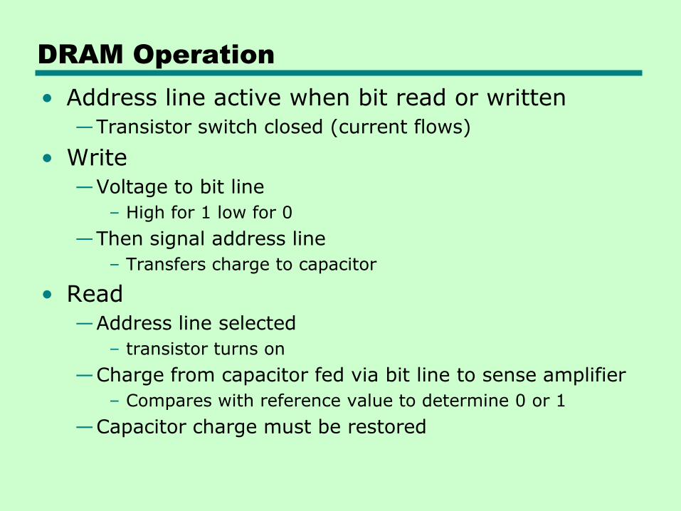
• Address line active when bit read or written
—Transistor switch closed (current flows)
• Write
—Voltage to bit line
– High for 1 low for 0
—Then signal address line
– Transfers charge to capacitor
• Read
—Address line selected
– transistor turns on
—Charge from capacitor fed via bit line to sense amplifier
– Compares with reference value to determine 0 or 1
—Capacitor charge must be restored

Static RAM
• Bits stored as on/off switches
• No charges to leak
• No refreshing needed when powered
• More complex construction
• Larger per bit
• More expensive
• Does not need refresh circuits
• Faster
• Cache
• Digital
—Uses flip-flops

SRAM Cell Structure

Static RAM Operation
• Transistor arrangement gives stable logic state
• State 1—C1 high, C2 low
—T1 T4 off, T2 T3 on
• State 0—C2 high, C1 low
—T2 T3 off, T1 T4 on
• Address line transistors T5 T6 is switch
• Write – apply value to B & compliment to B
• Read – value is on line B

SRAM v DRAM
• Both volatile
—Power needed to preserve data
• Dynamic cell
—Simpler to build, smaller
—More dense
—Less expensive
—Needs refresh
—Larger memory units
• Static
—Faster
—Cache

Read Only Memory (ROM)
• Permanent storage
—Nonvolatile
• Used to store:
—Microprogramming (see later)
—Library subroutines
—Systems programs (e.g. BIOS)
—Function tables
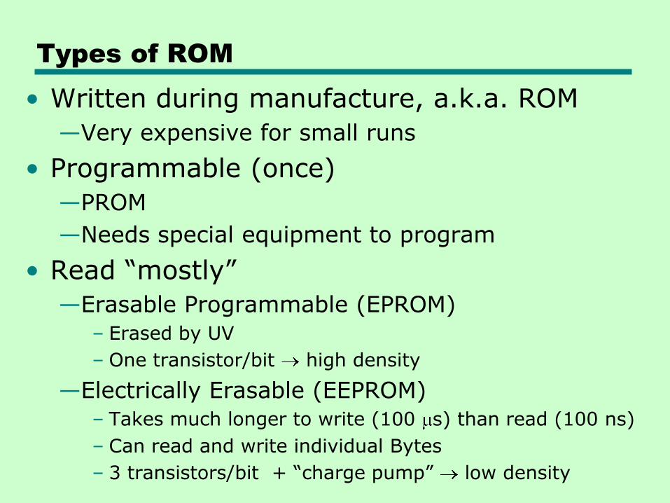
Types of ROM
• Written during manufacture, a.k.a. ROM
—Very expensive for small runs
• Programmable (once)
—PROM
—Needs special equipment to program
• Read ―mostly‖
—Erasable Programmable (EPROM)
– Erased by UV
– One transistor/bit high density
—Electrically Erasable (EEPROM)
– Takes much longer to write (100 s) than read (100 ns)
– Can read and write individual Bytes
– 3 transistors/bit + ―charge pump‖ low density
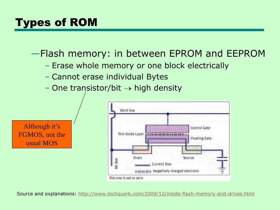
Types of ROM
—Flash memory: in between EPROM and EEPROM
– Erase whole memory or one block electrically
– Cannot erase individual Bytes
– One transistor/bit high density
Source and explanations: http://www.techquark.com/2009/12/inside-flash-memory-and-drives.html
Although it’s
FGMOS, not the
usual MOS
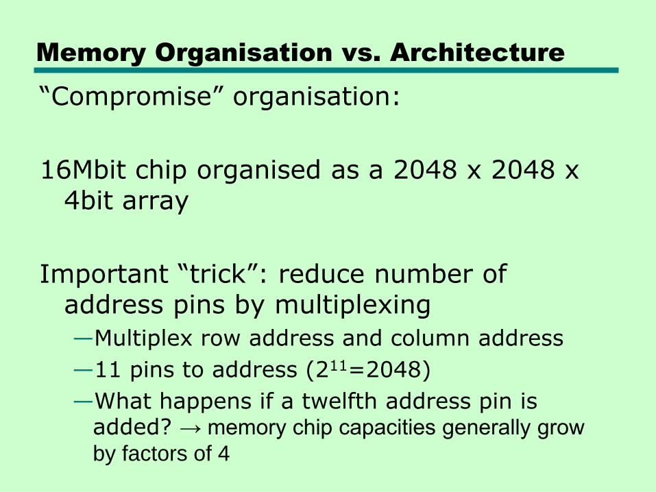
Memory Organisation vs. Architecture
Example architecture:
• The programmer wants a total of 16 Mbit (= 2 MB) of memory, with a word size of 16 bit
This could be organized in two extreme ways:
• The word-per-chip system: One chip, containing 1 Million (220) 16-bit words
• The bit-per-chip system: 16 chips, each containing 1 Million 1-bit words
—Accessing a word means accessing (in parallel!) its 16 bits, one from each chip
Memory Organisation vs. Architecture
―Compromise‖ organisation:
16Mbit chip organised as a 2048 x 2048 x 4bit array
Important ―trick‖: reduce number of address pins by multiplexing
—Multiplex row address and column address
—11 pins to address (211=2048)
—What happens if a twelfth address pin is added? → memory chip capacities generally grow
by factors of 4

Simplified DRAM Read Timing (p.181 of our text)
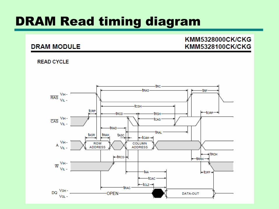
DRAM Read timing diagram

Typical 16 Mb DRAM (4M x 4)
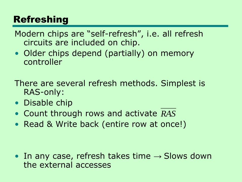
Refreshing
Modern chips are ―self-refresh‖, i.e. all refresh circuits are included on chip.
• Older chips depend (partially) on memory controller
There are several refresh methods. Simplest is RAS-only:
• Disable chip
• Count through rows and activate
• Read & Write back (entire row at once!)
• In any case, refresh takes time → Slows down the external accesses
RAS

Packaging
Explain how to connect
CE for 2 and 4 chips
How is the function of WE
and OE performed on the
EPROM chip?

Putting the
memory chips
together in a
module
Example:
256 kByte Module
made of 256 k x 1
chips
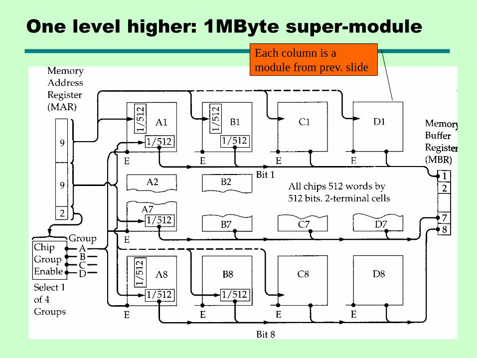
One level higher: 1MByte super-module
Each column is a
module from prev. slide

Interleaved Memory
A collection of DRAM chips can be:
• A memory module (as on prev. slides)
• A memory bank
• In a bank, consecutive words are stored on different chips
• K banks can service k requests (of consecutive words!) simultaneously—As in the case of caches, locality of reference
makes requests of consecutive words worthwhile
—What is being read may well be a block, going in a line of cache!

This concludes section 5.1
This is the material required for the midterm
To solve in notebook for next time:
End of chapter problems 5.2 and 5.3.
Next time:
• Review in class
• Exam in the lab

• Lost one lecture due to Dr. appt.

5.2 Error Correction
• Hard Failure
—Permanent physical defect
—Bit is ―stuck‖ at 0 or 1, or switches randomly
• Soft Error
—Random, non-destructive
—No permanent damage to memory
• Two types of codes:
—Only error detection
– E.g. even or odd parity bit
– E.g. ―Excess nine‖
—Error detection and correction
– E.g. Hamming code
Story from the early days
of the Univac …
Easy to implement using
XOR gates!
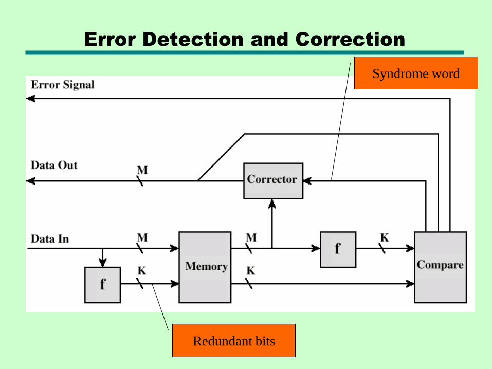
Error Detection and Correction
Redundant bits
Syndrome word
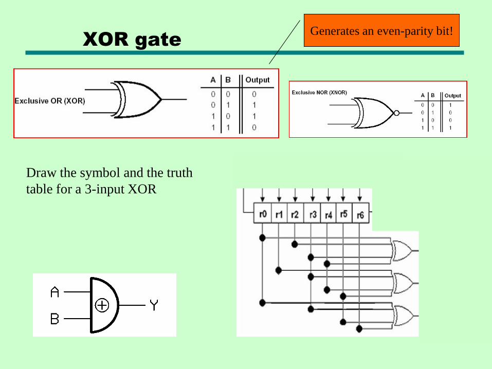
XOR gate
Draw the symbol and the truth
table for a 3-input XOR
Generates an even-parity bit!

4-bit example, using Venn diagram
Source: http://www.apl.ucl.ac.uk/lectures/3c42/3c42-13.htmlGo to the link for more examples and a nice discussion about possible
sources of errors!
Original 4 bits Adding K=3
parity bits
(even parity)
An error occurs.
How can we detect
and correct it?

8-bit example
• Problem: Venn diagrams with 4 or more bits become progressively harder to visualize
• Idea: Insert the parity bits in the word itself, in those positions which are powers of two
—Unlike normal bit numbering, start with position 1
Bit Position 12 11 10 9 8 7 6 5 4 3 2 1
Position
Number1100 1011 1010 1001 1000 0111 0110 0101 0100 0011 0010 0001
Data Bit D8 D7 D6 D5 D4 D3 D2 D1
Check Bit C8 C4 C2 C1
Figure 5.9 Layout of Data Bits and Check Bits
• FYI: on pp. 170-171 it is explained how to figure out the exact number of parity bits for a code that corrects 1 error.
• However, the method of construction of the Hamming code explained on the prev. slide already has this number built-in automatically!
—We simply stop inserting bits when we’ve run out of original bits

Back to our 8-bit example …
Bit
position12 11 10 9 8 7 6 5 4 3 2 1
Position
number1100 1011 1010 1001 1000 0111 0110 0101 0100 0011 0010 0001
Data bit D8 D7 D6 D5 D4 D3 D2 D1
Check
bitC8 C4 C2 C1
Word
stored as 0 0 1 1 0 1 0 0 1 1 1 1
Word
fetched
as
0 0 1 1 0 1 1 0 1 1 1 1
Position
Number1100 1011 1010 1001 1000 0111 0110 0101 0100 0011 0010 0001
Check
Bit0 0 0 1
Figure 5.10 Check Bit Calculation
Each check bit is calculated as an even-parity bit over those data bits whose
position numbers contain the respective power of 2 (it’s a lot easier in binary!)
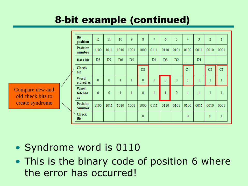
8-bit example (continued)
• Syndrome word is 0110
• This is the binary code of position 6 where the error has occurred!
Compare new and
old check bits to
create syndrome
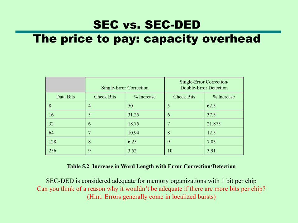
SEC vs. SEC-DED
The price to pay: capacity overhead
Table 5.2 Increase in Word Length with Error Correction/Detection
SEC-DED is considered adequate for memory organizations with 1 bit per chip
Can you think of a reason why it wouldn’t be adequate if there are more bits per chip?
(Hint: Errors generally come in localized bursts)
Single-Error Correction
Single-Error Correction/
Double-Error Detection
Data Bits Check Bits % Increase Check Bits % Increase
8 4 50 5 62.5
16 5 31.25 6 37.5
32 6 18.75 7 21.875
64 7 10.94 8 12.5
128 8 6.25 9 7.03
256 9 3.52 10 3.91
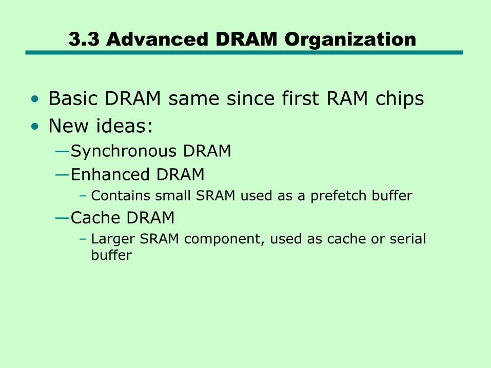
3.3 Advanced DRAM Organization
• Basic DRAM same since first RAM chips
• New ideas:
—Synchronous DRAM
—Enhanced DRAM
– Contains small SRAM used as a prefetch buffer
—Cache DRAM
– Larger SRAM component, used as cache or serial buffer

Synchronous DRAM (SDRAM)
• Access is synchronized with an external clock
• Address is presented to RAM
• RAM finds data (CPU waits in conventional DRAM)
• Since SDRAM moves data in time with system clock, CPU knows when data will be ready
• CPU does not have to wait, it can do something else
• Burst mode allows SDRAM to set up stream of data and fire it out in block
• DDR-SDRAM sends data twice per clock cycle (leading & trailing edge)
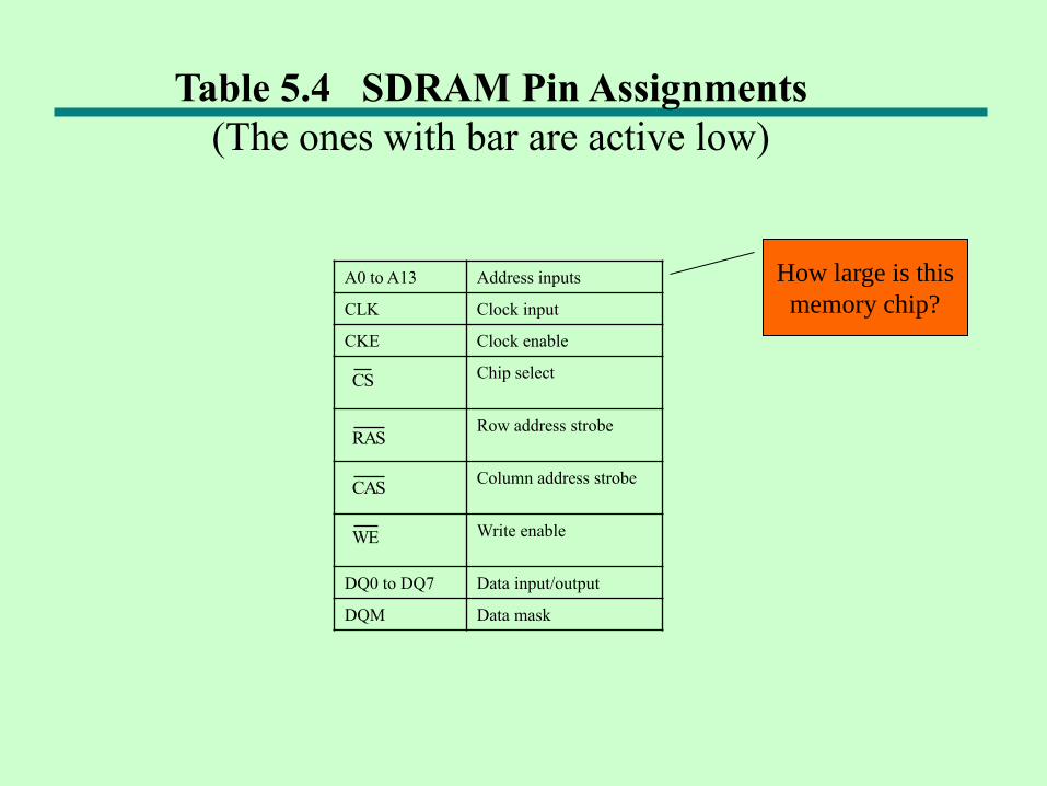
A0 to A13 Address inputs
CLK Clock input
CKE Clock enable
Chip select
Row address strobe
Column address strobe
Write enable
DQ0 to DQ7 Data input/output
DQM Data mask
CS
RAS
CAS
WE
Table 5.4 SDRAM Pin Assignments
(The ones with bar are active low)
How large is this
memory chip?
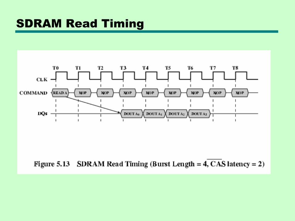
SDRAM Read Timing

IBM 64 Mb SDRAM
We have covered pp.169-176.
Read and take notes!
Solve problem 5.10!

Lab week 7
End of chapter problems
• 2
• 3
• 9
• 10
• 11
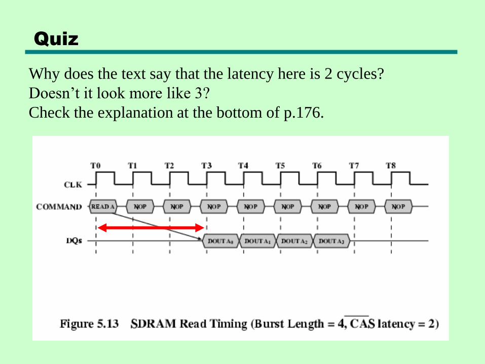
Quiz
Why does the text say that the latency here is 2 cycles?
Doesn’t it look more like 3?
Check the explanation at the bottom of p.176.
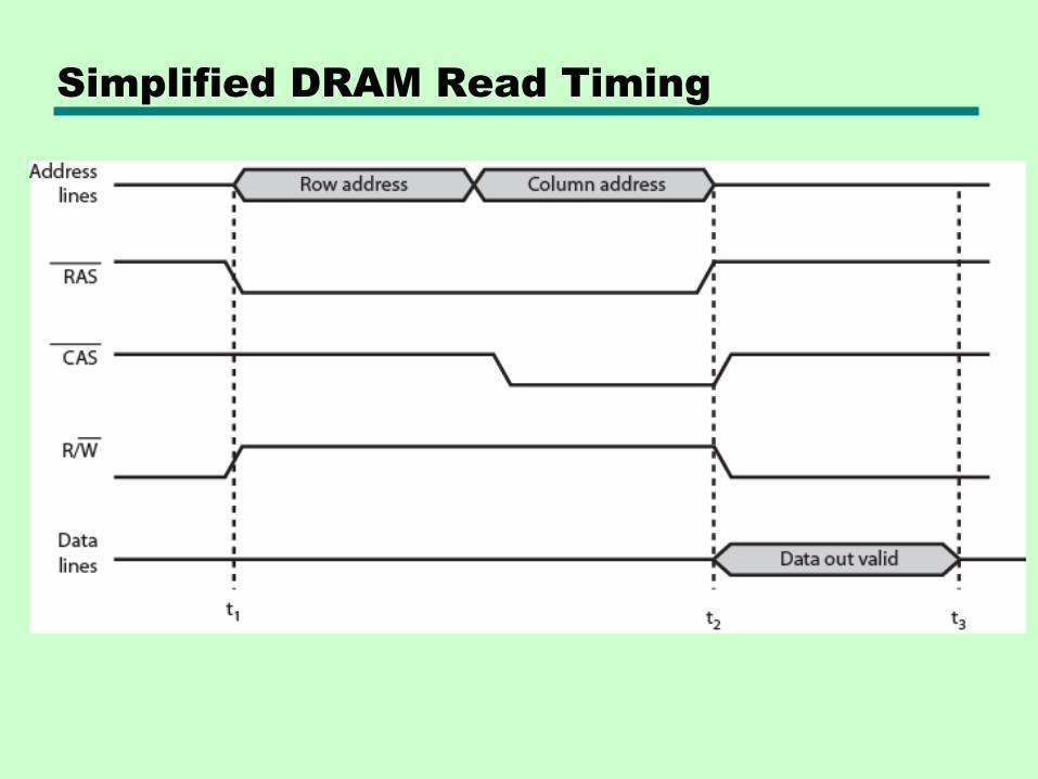
Simplified DRAM Read Timing

RAMBUS DRAM
• Adopted by Intel for Pentium & Itanium
• Main competitor to SDRAM
• Vertical package – all pins on one side
• Data exchange over 28 wires < 12 cm long
• Bus addresses up to 320 RDRAM chips at 1.6Gbps
• Asynchronous block protocol
—480ns access time
—Then 1.6 Gbps
Why a distance
limitation?
Attenuation!

RAMBUS Diagram
No more RAS, CAS, etc. A more complex request is sent over the address + control
part of the bus (RC = Rambus Control).
Electrical termination
(as in the old Ethernet
cables!)
18 = 16 data + 2 parity

RAMBUS in Real Life
Did Intel’s choice of RAMBUS ―cripple‖ the Pentium 4?
Read this:
SystemLogic.net - Why Intel Is Twofaced
DDR SDRAM
• SDRAM can only send data once per clock
• Double-data-rate SDRAM can send data twice per clock cycle
—Rising edge and falling edge
—Note: RAMBUS has DDR, too!

DDR SDRAM
Read Timing

Cache DRAM
• Mitsubishi
• Integrates small SRAM cache (16 kb) onto generic DRAM chip
• Used as true cache
—64-bit lines
—Effective for ordinary random access
• To support serial access of block of data
—E.g. refresh bit-mapped screen
– CDRAM can prefetch data from DRAM into SRAM buffer
– Subsequent accesses solely to SRAM
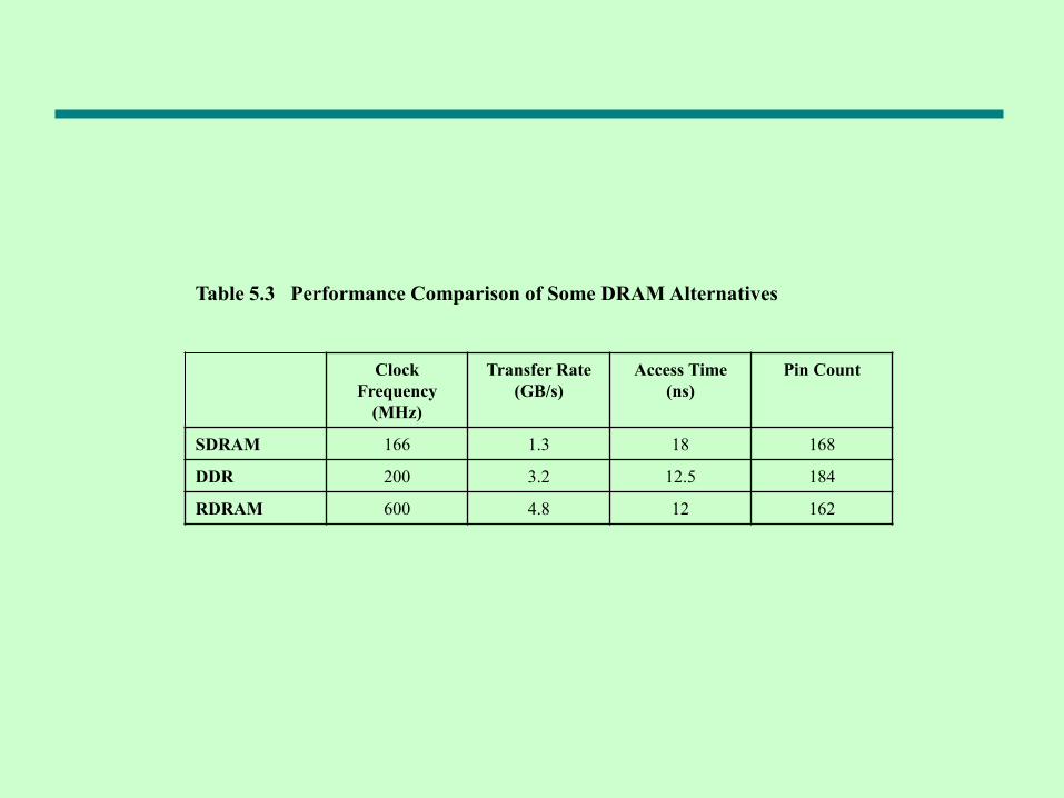
Table 5.3 Performance Comparison of Some DRAM Alternatives
Clock
Frequency
(MHz)
Transfer Rate
(GB/s)
Access Time
(ns)
Pin Count
SDRAM 166 1.3 18 168
DDR 200 3.2 12.5 184
RDRAM 600 4.8 12 162
Homework for Ch.5 Due Tue, Oct 26
End of chapter problems
• 6
• 12
• 13
• 14

Term Paper: DRAM Mysteries
• Covers two DRAM topics not mentioned in text:
— Fast Page Read
— 2k vs. 4k refresh
• Good starting point: Dynamic random access memory – Wikipedia
—Specifically, in the References section, make sure you download Micron 4 Meg x 4 EDO DRAM data sheet , which has nice timing and block diagrams
• To do: For each of the topics above, find at least two more references by Thursday’s lab