Embed Size (px)
Citation preview

1
0.13um Mixed Signal RF
Process Flow
TSS/FE 2012/12

2
GF 0.13um Technology

3
0.13um RF CMOS Overview

4
STI Formation
Well Formation
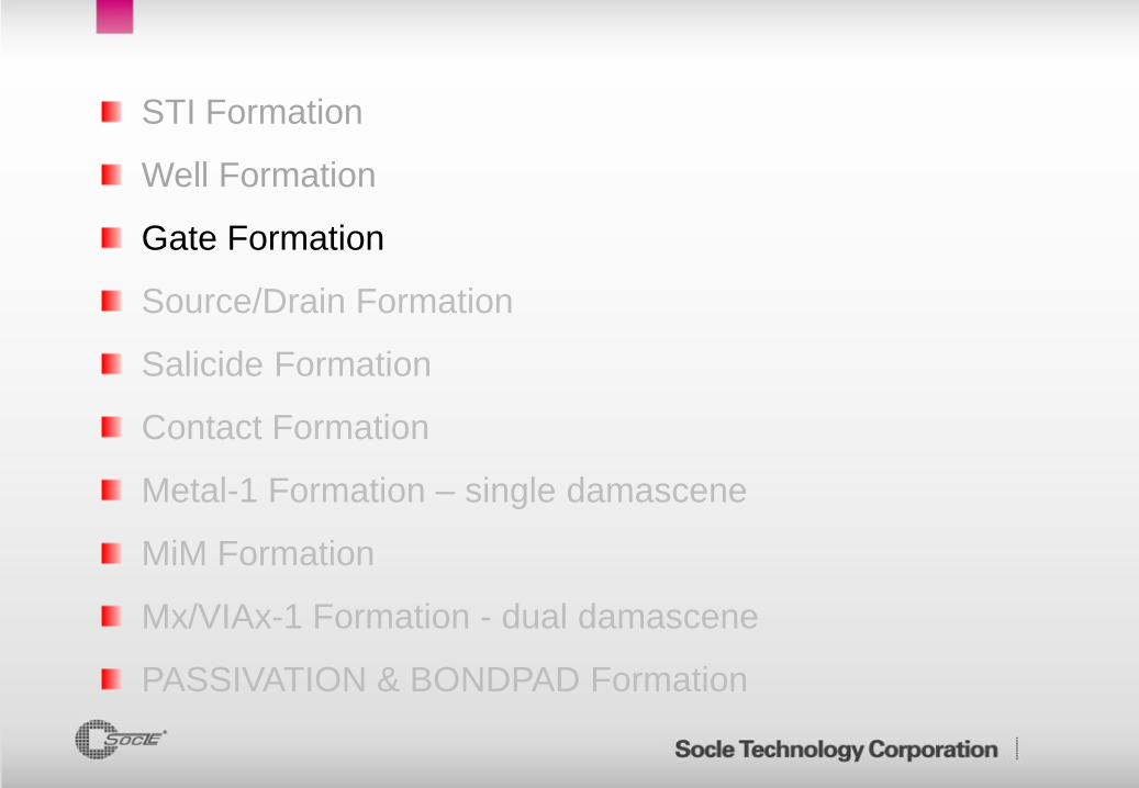
Gate Formation
Source/Drain Formation
Salicide Formation
Contact Formation
Metal-1 Formation – single damascene
MiM Formation
Mx/VIAx-1 Formation - dual damascene
PASSIVATION & BONDPAD Formation
Process Modules

STI Formation
Well Formation
Gate Formation
Source/Drain Formation
Salicide Formation
Contact Formation
Metal-1 Formation – single damascene
MiM Formation
Mx/VIAx-1 Formation - dual damascene
PASSIVATION & BONDPAD Formation

6
STI (Shallow Trench Isolation)
Deposit and pattern thin SiN (RX)
Si Substrate
STI Etch
STI gap fill – deposit SiO2
STI CMP
Wet SiN removal
SiN
RX (L10) Mask used to define active region.
Reverse(L11) Mask used;It is created by foundry and improve STI CMP uniformaity
and prevent Nitride residue.
Reverse active etch

STI Formation
Well Formation
Gate Formation
Source/Drain Formation
Salicide Formation
Contact Formation
Metal-1 Formation – single damascene
MiM Formation
Mx/VIAx-1 Formation - dual damascene
PASSIVATION & BONDPAD Formation

8
Well Implants Deep NWELL(optional) - deep N-well is for better isolation from substrate noise.(L06)
Core – Multi-Vt transistors:Low/Standard/High Vts,Native device
IO – 1.8V,2.5V or 3.3V,Native device
Photoresist
Deep NWELL
Deep NWELL
Deep NWELL
Deep NWELL
Deep NWELL
Deep NWELL
Deep NWELL
STI Formation
Well Formation
Gate Formation
Source/Drain Formation
Salicide Formation
Contact Formation
Metal-1 Formation – single damascene
MiM Formation
Mx/VIAx-1 Formation - dual damascene
PASSIVATION & BONDPAD Formation

10
Need two gate oxide thickness;Thin for core FETs and Thick for IO FETs
The gate oxide is grown in furnace,not deposited.It requires high quality to
have good reliability (Gate Oxide Integrity)
Dual Gate mask – L38
Gate Formation – (1) Dual Gate

11
1.Poly deposition
2.Poly gate mask(L60)
3. Poly gate etch
Gate Formation – (2) Poly Gate
The Poly CD control is critical and key to device performance.

STI Formation
Well Formation
Gate Formation
Source/Drain Formation
Salicide Formation
Contact Formation
Metal-1 Formation – single damascene
MiM Formation
Mx/VIAx-1 Formation - dual damascene
PASSIVATION & BONDPAD Formation

13
NLDD for Core and IO NFETs
1.Thin NLDD Mask(L61)
2.Thin NLDD Pocket Imp.
(P type)
3.Thin NLDD Imp.(N type)
1.Thick NLDD Mask(L62)
2.Thick NLDD Imp.(N type)
1.LDD (Lightly Doped Drain)is used for minimize peak E fields that cause hot
carrier and breakdown.
2.The NLDD must be heavily doped to minimize series resistance.

14
PLDD for Core and IO NFETs
1.Thin PLDD Mask(L64)
2.Thin PLDD Pocket Imp.
3.Thin PLDD Imp.
1.Thick NLDD Mask(L23)
2.Thick NLDD Imp.

15
Spacer Formation
1.Spacer deposition
2. Spacer etch (blanket)

16
Source / Drain Implantation
1.N source/drain mask(L65)
2.N source/drain imp.
3.N source/drain anneal
1.P source/drain mask(L70)
2.P source/drain imp.
3.P source/drain anneal

17
STI Formation
Well Formation
Gate Formation
Source/Drain Formation
Salicide Formation
Contact Formation
Metal-1 Formation – single damascene
MiM Formation
Mx/VIAx-1 Formation - dual damascene
PASSIVATION & BONDPAD Formation

18
1.
2.
3.
4.
Salicide Formation
1.Salicide block deposition
2.Salicide block mask (L68)
3.Salicide block etch
1.Cobalt deposition
Cobalt
1.1st RTA
2.Post RTA1 Cobalt remove
1.2nd RTA
The salicide is used to reduce Poly and diffusion Rs.
Technology progression: TiSix -> CoSix-> NiSix.Scaling requires smaller
silicide grain size to minimize Rs variations

STI Formation
Well Formation
Gate Formation
Source/Drain Formation
Salicide Formation
Contact Formation
Metal-1 Formation – single damascene
MiM Formation
Mx/VIAx-1 Formation - dual damascene
PASSIVATION & BONDPAD Formation

20
1.Etch-stop layer deposition
2.ILD deposition
3.ILD CMP
4.Contact mask (L75)
5.Contact etch
6.Barrier metal deposition
7.W(tungsten) deposition
8.W-CMP
Contact Formation

21
STI Formation
Well Formation
Gate Formation
Source/Drain Formation
Salicide Formation
Contact Formation
Metal-1 Formation – single damascene
MiM Formation
Mx/VIAx-1 Formation - dual damascene
PASSIVATION & BONDPAD Formation

22
M1 Formation- Single damascene
1.Etch-stop layer deposition
2.IMD deposition
3.Etch-stop layer deposition
4.Metal-1 mask (L80)
5.M1 Trench etch
6.Barrier seed deposition
7.Cu fill
8.Cu-CMP

23
STI Formation
Well Formation
Gate Formation
Source/Drain Formation
Salicide Formation
Contact Formation
Metal-1 Formation – single damascene
MiM Formation
Mx/VIAx-1 Formation - dual damascene
PASSIVATION & BONDPAD Formation

24
MiM (Metal insulator Metal)-Optional
MIM capacitor must be located between MetalTop layer and the metal layer immediately below
There are two options for MiM – 1-Mask and 2-Mask ;Below is the 1-Mask MiM
FuseTop layer(L92) defines the top plate and metal-[n-1] layer defines the bottom plate of the MIM capacitor.
The capacitance is 1.0 fF/um2

25
STI Formation
Well Formation
Gate Formation
Source/Drain Formation
Salicide Formation
Contact Formation
Metal-1 Formation – single damascene
MiM Formation
Mx/VIAx-1 Formation - dual damascene
PASSIVATION & BONDPAD Formation

26
Integration schemes for Dual Damascene
Mx/VIAx-1 Formation - dual damascene
1.Etch-stop layer deposition
2.IMD Via deposition
3.Etch-stop layer deposition
4.IMD Trench deposition
5.Etch-stop layer deposition
6.VIAx-1 mask (L85, L91, L94,
L97, L9R)
7.Dual damascene via etch
8.Mx mask(L88, L93, L96,
L9E, L98)
9.Barrier/seed deposition
10.Cu barrier
11.Cu deposition
12.Cu CMP
IMD(LK)
IMD(LK)

27
STI Formation
Well Formation
Gate Formation
Source/Drain Formation
Salicide Formation
Contact Formation
Metal-1 Formation – single damascene
MiM Formation
Mx/VIAx-1 Formation - dual damascene
PASSIVATION & BONDPAD Formation

28
1.Passivation-1 deposition (oxide + nitride)
2.L9C MASK + Etch
3.AL deposition
4.L9S MASK + ETCH
5.Passivation-2 deposition
6.L95 MASK + ETCH
7.Alloy
Passivation & Bond Pad Formation
L9C (L9S)
L95

29
Schematic Cross section

30
Thank you