Embed Size (px)
Citation preview
0.10.20.3
MICROELECTRONICS AND 0.4OPTOELECTRONICS LABORATORY 0.5
0.60.7
0.80.9
0.10
Substrate: 2 inch InP
Microelectronics & Optoelectronics Laboratory 1

0.110.120.130.140.150.160.170.180.190.200.21
Previous Page:
Optically controlled optical waveguide switches realized in Indium Phosphide asMach-Zehnder interferometers with semiconductor optical amplifiers in their arms
2 Institute of Quantum Electronics
CONTENTS 0.220.23
PERSONNEL 0.240.25
RESEARCH SUMMARY 0.26EDUCATIONAL ACTIVITIES 0.27ORBITUARY 0.28
0.29MICRO- AND OPTOELECTRONICS LABORATORY 0.30Three-Five Compound Semiconductor Device Fabrication Laboratory
Low Pressure Metal Organic Vapor Phase Epitaxy for III-V CompoundSemiconductors
Plasma Etching
Low Dimensional Semiconductor Nanostructures
Optically Controlled Mach-Zehnder Interferometer Switches for OpticalDemultiplexing and Wavelength Conversion
All-optical OTDM/WDM Transmultiplexer
All-Optical Signal Regeneration
40 Gbit/s Add/Drop Multiplexer
Modeling of All-Optical Mach-Zehnder Interferometer Switches
Fabrication of All Optical Switches
Principle of Flip-Chip-Mounted All-Optical-Switches
Cascadable MZI All-Optical Switch with a Data- and Control-SignalSeparation Scheme
Analysis of Electro-Optic Effects in InP / InGaAsP Based Waveguide Structures
Low loss waveguides based on InAlAs/InP
High Bit Rate Optical Pulse Sources
Wavelength Multiplexer Modules in Glass on Silicon
Fabrication of Phased Array Filters in InP Buried Multi-Quantum-WellWaveguide Structures
InGaAs/InP Photodiode Arrays for Optical Interconnects
Large Area PtSi-nSi Photodetectors with Stable Spectral Responsivityin the UV to soft X-ray Spectral Range
Microelectronics & Optoelectronics Laboratory 3

Polarization Insensitive Semiconductor Optical Amplifiers at 1.55 µmWavelength: Modeling, Fabrication and Integration
A New Concept for InP HBT Circuit Fabrication Technology
Monolithically Integrated 40Gb/s pin/HBT Optical Receiver Module
Electronic High-Speed, High-Current Driver Circuit
Laser Driver Circuits Implemented in CMOS Technology
Receivers for Optical Interconnects
CMOS Receiver Circuits for Optical Interconnects
Phase and Frequency Locked Multiphase Electronic Oscillator
Silicon Integrated Circuits for System Testing
Digital Optical Fibre Logic Modules
Microwave Photonics Using an External Cavity Diode Laser
Semiconductor Optical Amplifiers in Four-Wave Mixing System Experiments
Fibreoptic Telecommunications Education in Developing Countries
THIN FILM PHYSICS GROUP 0.310.32
Formation of Quantum Dots by Misfit Dislocation Superlattices
Monolithic Two-Dimensional PbTe Infrared Sensor Array on aRead-out Si-Chip
Infrared p-n junction sensors in epitaxial PbTe on Si(111) strucures
CdTe/CdS thin film solar cells
Growth and characterization of heteroepitaxial CuInySey layers andinterfaces
Wide gap chalcopyrites for advanced thin film solar cells
0.33
PUBLICATIONS AND ORAL PRESENTATIONS 1998 0.340.35
Micro- and Optoelectronics Laboratory
Thin Film Physics Group at Institute of Quantum Electronics
4 Institute of Quantum Electronics
, CR
STAFF 0.10.2
Head 0.3Melchior, Hans, Prof. Dr.
Optoelectronics and Microelectronics Laboratory 0.40.5
Academic and Corporate Guests 0.6Kneubühl, Fritz K., Prof. Dr.Ctyroky, Jiri, Ing., Dr.sc., Institute of Radio Engineering and Electronics, PragueSoto, Ortiz Horacio, Dr., CICESE, Ensenada, MexicoTomkos, Ioannis, Msc. Eng., University of Athens , GreeceZacharopulos, Ioannis, Msc. Eng., University of Athens , GreeceDall’Ara, Roberto, Opto Speed SA, Mezzovico, SwitzerlandBlaser, Hanspeter, Opto Speed SA, Mezzovico, SwitzerlandRezzonico, Raffaele, Opto Speed SA, Mezzovico, SwitzerlandValerio, Igor, Opto Speed SA, Mezzovico, Switzerland
Team Leaders 0.7Guekos, Georg, Dr., Associate ProfessorSchmid, Jürg, Dr., Lecturer
Academic Staff 0.8Alimkulova, Lisa, Dipl. Phys. Univ. KasachstanAnnen, Richard, Dipl. El.-Ing. ETHBauknecht, Raymond, Dr.sc.nat. ETHBitter, Martin, Dipl. El.-Ing. ETHBlaser, Markus, Dr. sc.techn. ETHBossard, Martin, Dipl. El.-Ing. ETHCaraccia-Gross, Muriel, Dipl. Phys. ETHDülk, Marcus, Dipl. Phys. TU BerlinEckner, Jürg, Dr. sc.nat. ETHFischer, Stefan, Dipl. Phys. ETHGamper, Emil, Dipl. Phys. ETHGini, Emilio, Dr. sc.nat. ETHGirardin, François, Dr. es sciences ENST, ParisHagn, Gerhard, Dipl. Phys. ETHHess, Rolando, Dr.sc.nat. ETHHoltmann, Christoph, Dr. sc.nat. ETHHunziker, Werner, Dr. sc.nat. ETH
Microelectronics & Optoelectronics Laboratory 5

.ch
Krähenbühl, Roger, Dr.sc.nat. ETHLai, Qun, Dr.sc.techn. ETHLanker, Michael, Dipl. Phys. ETHLe Pallec, Michel, Ph.D. Inst. Nat. Polytech. GrenobleLeuthold, Jürg, Dipl. Phys. ETHMoretti, Patrick, Dipl. El.-Ing. ETHNadler, Christoph, Dipl. Phys. ETHNizzola, Pietro C., Dr.sc.techn. ETHOcchi, Lorenzo, Dipl. El.-Ing. ETHPajarola, Stephan, Dr.sc.techn. ETHSchmid, André, Dipl. El.-Ing. ETHSchneibel, Hanspeter, Dipl. El.-Ing. ETHSolt, Katalin, Dr. sc.nat., ETHVélez, Christian, Dipl.Phys. ETHVogt, Werner, Dr. sc.nat. ETHWieland, Jörg, Dr. sc.techn. ETHWildermuth, Eberhard, Dipl. Phys. L.M. Univ. MunichZenklusen, Patrick, Dipl. El.-Ing. ETH
Technical Staff 0.9Bolz, EdmundEbnöther, MartinGraf, Christoph, Dipl. El.-Ing. HTLGu-Zhong, Ming, Dipl. El.Ing. Chengdu Univ. P.R. ChinaMüller, AndreasTamburello, Giuseppe, Dipl. El.-Ing. HTL
Administrative Staff 0.10Bürgisser, Veronica Pfammatter, PauletteDekker, Wendy Spena, Sonja
Microelectronics and Optoelectronics Laboratory 0.11Prof. Dr. H. Melchior Prof. Dr. G. GuekosTel. : +41 1 633 21 01 Tel. : +41 1 633 20 85Fax : +41 1 633 11 09 Fax : +41 1 633 11 09E-mail: [email protected] E-mail : [email protected]
Institute of Quantum Electronics http://www.iqe.ethz.ch/me+oe/Swiss Federal Institute of TechnologyCH-8093 Zurich, Switzerland
6 Institute of Quantum Electronics
landlanddntral
y ofgaria
Thin Film Physics Group 0.12
Group Leader 0.13Zogg, Hans, Dr. sc.nat. ETH, PD, Lecturer
Leader Photovoltaics 0.14Tiwari, Ayodhya Nath, Dr. phil.sc. Indian Institute of Technology Dehli, India
Academic and Corporate Visitors 0.15Boyko, Borys, Prof. Dr., Kharkov State Polytechnic University, Kharkov/UkraineKhrypunov, Gennadiy, Associate Prof., Kharkov State Polytechnic University,Kharkov/UkraineKharchenko, Mykola, Eng.-Phys., Kharkov State Polytechnic University, UkraineIgalson, Malgorzata, Associate Prof. Dr., Warsaw University of Technology, PoZabierowski, Pawel, Msc. Eng/Ph.D. Stud., Warsaw University of Technology, PoWimbor, Magdalena Izabella, Student, Warsaw University of Technology, PolanStratieva Radkova, Natalia, Associate Prof., Bulgarian Academy of Sciences, CeLaboratory on Solar Energy & New Energy Sources, Sofia/BulgariaRachenov Radoslav, Stefanov, Dr., Senior Research Fellow, Bulgarian AcademSciences, Central Laboratory on Solar Energy & New Energy Sources, Sofia/Bul
Academic Staff 0.16Alchalabi, Karim, Dipl.Phys. University of Freiburg, GermanyAthanassov, Yordan, Dr.sc.nat. EPFLBätzner, Derk Leander, Dipl.Phys. University of Köln, GermanyHaug, Franz-Josef, Dipl.Phys. University of Ulm, GermanyJohn, Joachim, Dipl.Phys. University of Freiburg, GermanyKrejci, Martin, Dipl.Phys. ETH Zürich, SwitzerlandRomeo, Alessandro, Dipl.Phys. University of Parma, Italy
Technical Staff 0.17Leopold, MichaelSchreiber, GerhardWerner, Thomas
Thin Film Physics Group 0.18Technopark ETH-TraktTechnoparkstrasse 1CH-8005 Zürich, SwitzerlandTel. : +41 1 445 14 80Fax : +41 1 445 14 99
Microelectronics & Optoelectronics Laboratory 7

8 Institute of Quantum Electronics
ily onilt-uppit-d high-tion ofp of
oratorywell asemi-activ-opto-fiber
ng,
in-s for
ctive
alized
ithized
, in-
ave-
siond effi-
at 60
RESEARCH SUMMARY 0.19
The research activities of the Microelectronics and Optoelectronics Laboratory rely heavthe three-five compound semiconductor epitaxy and device development capability, buwithin the group over the years. Its Metal-Organic Chemical Vapor Deposition (MOCVD) eaxy serves, on one hand, for the development of optoelectronic waveguide components anspeed electronics in Indium Phosphide quaternaries, and on the other hand, for the realizaquantum-well and quantum-wire structures in Gallium Aluminium Arsenide through the grouProf. E. Kapon of the École Polytechnique Fédérale de Lausanne. Three scientists, a labtechnician and all the device developers share the technology and device developments asthe running and maintenance of the device fabrication facility. The three-five compound sconductor physics and optoelectronics device technology capabilities are flanked by designities in silica on silicon optical waveguide components and in high-speed electronics. Theelectronics and high-speed electronics research is essentially driven by applications inoptical communications.
Research highlights of 1998:• Optically controlled optical waveguide switches for multi-ten Gigabit/s signal multiplexi
demultiplexing and wavelength conversion.
• Optically controlled optical switch modules consisting of monolithic InP Mach-Zehnderterferometer with semiconductor optical amplifiers in their arms and waveguide-taperlow loss coupling to optical fibers.
• Physical modeling of optically controlled waveguide switches taking picosecond refraindex- and gain dynamics into account.
• Forty Gigabit/sec photodetector receivers for 1.3 and 1.55 micrometer wavelengths rein InGaAs/InP-photodiode-heterobipolar transistor technology.
• Wavelength-division-multiplex (WDM) filters in silica on silicon featuring 16 channels wlow insertion loss, low crosstalk and complete insensitivity to polarization at standard200 GHz-spaced frequencies in the 1.55 micrometer wavelength range.
• Thermooptic silica on silicon waveguide switches with submillisecond switching timessertion losses below 1 dB and on-off ratios exceeding 20 dB.
• Semiconductor optical amplifiers and amplifier gates for 1,3 and 1,55 micrometer wlengths featuring high polarization independent gains.
• Quantum Hall effect devices in an effort with the group of Prof. Ensslin.
• Four wave mixing in semiconductor optical amplifiers, resulting in wavelength converover 30 nm at 10 Gb/s, dispersion compensation by mid-span spectral inversion, anciency flattening and equalization of frequency up- and down-conversion.
• Microwave photonics and data transmission on optically generated millimeter-wavesGHz using a dual-polarisation emission external cavity diode laser.
Microelectronics & Optoelectronics Laboratory 9

NOT,
pticale op-s-
theNET,y fi-TA.
pletedOST-
, thewer-ledgeeen our
pmentsctively, Mez-
Dr.tors,
elldare de-ition
Te on
e on
l lay-
• Semiconductor optical amplifier assisted Sagnac interferometer and applications asAND and XOR gates, and all-optical shift register at 10 GHz.
Several of the optoelectronic and high-speed electronic device developments for fiber ocommunication projects of the European Union (EU) are coming to completion. They includtically controlled optical time domain demultiplexer/wavelength division (OTDM/WDM) tranmultiplexers for the ACTS Project OPEN, InP space switches, SiO2/Si wavelength-division-multiplex-(WDM)filters and Gigabit/s 200 mA driver electronics for optical amplifier gates ofACTS KEOPS project, photodetectors, transmitter- and receiver-electronics for the COBWOTAN and RODCI projects. Ongoing projects include internal as well as directly industrnanced and national foundation projects, and the EU-projects HIGHWAY, OIIC and SONAIn addition, we are involved in the European COST-framework, have co-ordinated and coma COST-project on photonic devices for telecommunications, and are active in several Cprojects in telecommunications and physics.
We acknowledge the support of the "Bundesamt für Bildung und Wissenschaft (BBW)""Swiss Nationalfonds", the "Kommission für Technologie und Innovation" and the Schpunkts-Programm Optique of the Swiss Federal Institute of Technology. We also acknowthe support by the Japanese Ministry of Postal Services for the research co-operation betwgroup and the Yamagata University.
We are encouraged, that several of our optoelectronics device and packaging develoand optical interconnect transmitter and receiver designs are of interest to industry and aexploited commercially, thereby creating jobs at two start-up companies: Opto Speed SAzovico, Ticino and Helix AG, Zurich.
TheThin Film Physics Group, associated with our laboratory, is, under the leadership ofZogg and Dr. Tiwari, active in the physics and development of compound semiconducsuch as PbTe/PbSnSe, CuInSe2, CuGaSe2 and CdTe/Cds for infrared detection and solar cdevelopment. In addition, wide bandwidth AlGaAs/CaF2 quarter wavelength stack mirrors ansaturable absorbers intended as key elements for the generation of ultrashort laser pulsesveloped (see report of Prof. U. Keller). For layer growth, various physical vapour deposmethods, including MBE (Molecular Beam Epitaxy) are used.
Highlights of 1998 include:Narrow bandgap materials for infrared sensors:• One- and 2-dimensional infrared sensor arrays for thermal imaging in e.g. epitaxial Pb
Si-substrates that may contain active circuits.
• Study and reduction of dislocations to <106 cm-2 in lattice mismatched epitaxial PbSSi(111).
Solar cell research:• Fabrication processes for polycrystalline CuInGaSe2 thin film solar cells with ~14% effi-
ciency.
• CdTe solar cells with 11% efficiency by vacuum evaporation and recrystallization.
• Highly transparent (>85%) and conducting (sheet resistance < 10 Ohms/square ZnO:Aers grown by RF magnetron sputtering.
10 Institute of Quantum Electronics
on
u-
Thins andurs-oursetwo-
wo-se-ly in-
d eight
to en-l yearssup-
• Growth of CuIn2.5Se4 single phase epitaxial layers and aqueous solution epitaxy of CdSCuInSe2.
• Identified nanometer sized CuxSe precipitates, limiting the photovoltaic properties of Crich CuGaSe2 solar cells.
Educational Activities 0.20
The teaching activities of the Microelectronics and Optoelectronics Laboratory and of theFilm Physics Group in 1998 included a two-semester course in Semiconductor ElectronicIntegrated Circuits with device fabrication in the laboratory by H. Melchior and J. Schmid, coes in Fiber Optical Communication and Optoelectronics by G. Guekos and H. Melchior, a cin Diode Lasers and Optoelectronics by H. Melchior, a course in Solar Cells by G. Guekos, asemester course in Electronics for physics students by J. Schmid and R. Zinniker and a tmester course in Thin Film Physics and Technology by H. Zogg. The group is also activevolved in laboratory exercises for physics and electrical engineering students.
Our research and educational activities in 1998 resulted in several diploma theses andoctoral theses.
We are engaged in helping universities and research institutions in developing countrieshance their teaching and research capabilities in fiber optical communications. Since severawe are involved in the organisation of regional courses in South-East Asia and Africa and weport practical work in local laboratories.
Microelectronics & Optoelectronics Laboratory 11

ourroundevice
stud-ree inilicon
ute oftoraldevel-e het-
, pro-up and
ORBITUARY 0.1
On January 2nd, 1999
Dr. Jürg Schmid,
our longtime groupleader, lecturerand specialist in semiconductor
technology and device fabricationpassed away quite unexpectedly.
He died from a heart-attack.
In Dr. Jürg Schmid we loose the scientist who contibuted the most both to puttingthree-five compound semiconductor device technology laboratory in place and to instigateprocedures for its operation. In addition, Jürg Schmid was very creative in developing new dprocesses and electronic circuits.
Jürg Schmid was born March 11th, 1946 in Zurich, where he also went to school. Heied physics at the Swiss Federal Institute of Technology in Zurich, earning a Physics Deg1971. From 1972 to 1974 he worked as silicon device technology developer for the Swiss sintegrated circuit manufacturer FASELEC. In 1975 he returned to the Swiss Federal InstitTechnology, first to head a small silicon integrated circuit laboratory and to complete a docthesis. Then he became lecturer in electronics and was leading a group responsible for theopment of three-five compound semiconductor technology and high-speed indium phosphiderobipolar transistors.
Jürg Schmid was very talented in device technology developments. With his ideasfound technology knowhow and his sound judgement, he helped and inspired the entire grohis students.
He leaves behind his wife Verena and his son Martin.
12 Institute of Quantum Electronics

elop-com-.ers,ipolar(the
logyg ca-mi-
Three-Five Compound Semiconductor Device FabricationLaboratory 0.2E. Gini, J. Schmid, W. Vogt, R. Bauknecht, M. Blaser, M. Bitter , E. Gamper, C. Holt-mann, M. Ebnöther and H. Melchior
For the optoelectronic waveguide device and the high-speed electronics devments, the microelectronics and optoelectronics group relies on a three-fivepound semiconductor device laboratory that has been built-up over the yearsMetalorganic chemical vapor deposition (MOCVD) serves to grow epitaxial layboth InP-based optoelectronic waveguide devices and high-speed heterobelectronics and for GaAs-based multi-quantum-well and quantum-wire laserslater for Prof. E. Kapon and his group at the Swiss Federal Institute of Technoin Lausanne). The epitaxy growth facility is complemented by planar processinpabilities, including contact lithography, plasma- and wet etching, thin film checal vapor deposition, evaporation and sputtering.
Microelectronics & Optoelectronics Laboratory 13
14 Institute of Quantum Electronics
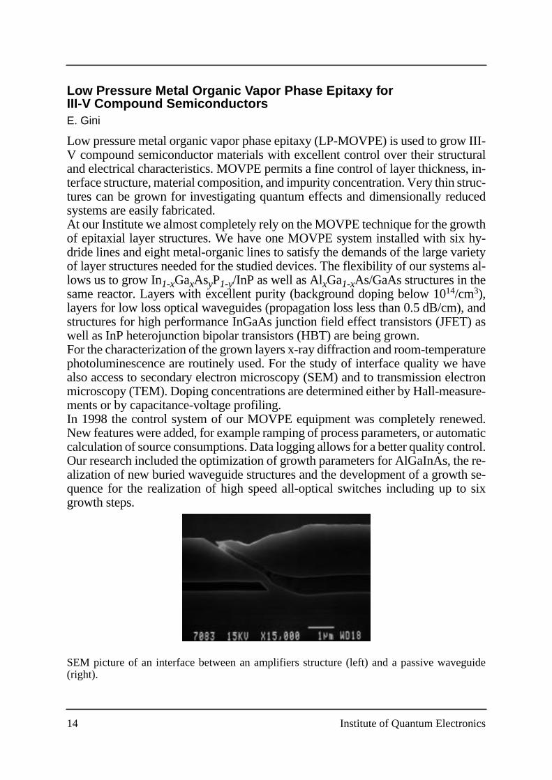
Low Pressure Metal Organic Vapor Phase Epitaxy forIII-V Compound Semiconductors 0.1E. Gini
Low pressure metal organic vapor phase epitaxy (LP-MOVPE) is used to grow III-V compound semiconductor materials with excellent control over their structuraland electrical characteristics. MOVPE permits a fine control of layer thickness, in-terface structure, material composition, and impurity concentration. Very thin struc-tures can be grown for investigating quantum effects and dimensionally reducedsystems are easily fabricated.At our Institute we almost completely rely on the MOVPE technique for the growthof epitaxial layer structures. We have one MOVPE system installed with six hy-dride lines and eight metal-organic lines to satisfy the demands of the large varietyof layer structures needed for the studied devices. The flexibility of our systems al-lows us to grow In1-xGaxAsyP1-y/InP as well as AlxGa1-xAs/GaAs structures in thesame reactor. Layers with excellent purity (background doping below 1014/cm3),layers for low loss optical waveguides (propagation loss less than 0.5 dB/cm), andstructures for high performance InGaAs junction field effect transistors (JFET) aswell as InP heterojunction bipolar transistors (HBT) are being grown.For the characterization of the grown layers x-ray diffraction and room-temperaturephotoluminescence are routinely used. For the study of interface quality we havealso access to secondary electron microscopy (SEM) and to transmission electronmicroscopy (TEM). Doping concentrations are determined either by Hall-measure-ments or by capacitance-voltage profiling.In 1998 the control system of our MOVPE equipment was completely renewed.New features were added, for example ramping of process parameters, or automaticcalculation of source consumptions. Data logging allows for a better quality control.Our research included the optimization of growth parameters for AlGaInAs, the re-alization of new buried waveguide structures and the development of a growth se-quence for the realization of high speed all-optical switches including up to sixgrowth steps.
SEM picture of an interface between an amplifiers structure (left) and a passive waveguide(right).

plica-
rat-ctors
ptical
orderEtch
with-n theashr con-nu al-dry-dge.
Plasma Etching 0.3E. Gini
Today, state-of-the-art integrated circuit manufacture depends on the mass retion of tightly controlled, micron-sized features in a multeity of materials.At our Institute a variety of equipment for the dry etching of optoelectronic integed circuits is available. Commonly used are two conventional parallel plate reaas schematically described in the figure below .
Plasma etching processes for the definition of InP based waveguides and oswitch structures are based on mixtures of the gases H2, CH4 and Ar. Process pa-rameters as gas flows, chamber pressure, RF power density are optimized into achieve a high selectivity to the mask materials and a good homogeneity.depth variations as low as±1.5% have been achieved over a 2-inch wafer.The same type of system is used for the dry etching of Ti and SiOx layers using flu-orine chemistry. These layers are used as mask material that are capable tostand high temperatures. The etching of optical silica waveguides is done osame system. In addition we have the capability to etch polyimide, PMMA or toorganic residues with an oxygen plasma. Both etching systems are computetrolled and a number of standard processes are installed. A user-friendly melows people from our but also from external reserarch groups to run theiretching processes themselves without the need of profound technical knowle
13.56 MHz
Pump
Gas inlet
PlasmaSheaths
CathodeSamples
V
DC bias
Schematic view of a parallel plate reactor.generator
Microelectronics & Optoelectronics Laboratory 15
evalu-lec-andl Va-cent
non-l fea-self-t the
oury ofes in
for theeriorenses in
iond usn 1Dlar re-antnce-
wasn thee andent inR
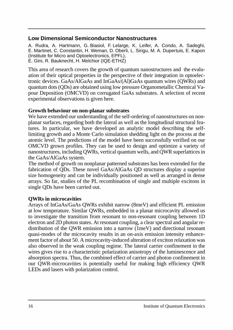
Low Dimensional Semiconductor Nanostructures 0.4A. Rudra, A. Hartmann, G. Biasiol, F. Lelarge, K. Leifer, A. Condo, A. Sadeghi,E. Martinet, C. Constantin, H. Weman, D. Oberli, L. Sirigu, M. A. Dupertuis, E. Kapon(Institute for Micro and Optoelectronics, EPFL),E. Gini, R. Bauknecht, H. Melchior (IQE-ETHZ)
This area of research covers the growth of quantum nanostructures and theation of their optical properties in the perspective of their integration in optoetronic devices. GaAs/AlGaAs and InGaAs/(Al)GaAs quantum wires (QWRs)quantum dots (QDs) are obtained using low pressure Organometallic Chemicapour Deposition (OMCVD) on corrugated GaAs substrates. A selection of reexperimental observations is given here.
Growth behaviour on non-planar substratesWe have extended our understanding of the self-ordering of nanostructures onplanar surfaces, regarding both the lateral as well as the longitudinal structuratures. In particular, we have developed an analytic model describing thelimiting growth and a Monte Carlo simulation shedding light on the process aatomic level. The predictions of the model have been successfully verified onOMCVD grown profiles. They can be used to design and optimize a varietnanostructures, including QWRs, vertical quantum wells, and QWR superlatticthe GaAs/AlGaAs system.The method of growth on nonplanar patterned substrates has been extendedfabrication of QDs. These novel GaAs/AlGaAs QD structures display a supsize homogeneity and can be individually positioned as well as arranged in darrays. So far, studies of the PL recombination of single and multiple excitonsingle QDs have been carried out.
QWRs in microcavitiesArrays of InGaAs/GaAs QWRs exhibit narrow (8meV) and efficient PL emissat low temperature. Similar QWRs, embedded in a planar microcavity alloweto investigate the transition from resonant to non-resonant coupling betweeelectron and 2D photon states. At resonant coupling, a clear spectral and angudistribution of the QWR emission into a narrow (1meV) and directional resonquasi-modes of the microcavity results in an on-axis emission intensity enhament factor of about 50. A microcavity-induced alteration of exciton relaxationalso observed in the weak coupling regime. The lateral carrier confinement iwires gives rise to a characteristic polarization anisotropy of the luminescencabsorption spectra. Thus, the combined effect of carrier and photon confinemour QWR-microcavities is potentially useful for making high efficiency QWLEDs and lasers with polarization control.
16 Institute of Quantum Electronics
em-the
n-onthe
esultsla-
tingtorialsure-ma-peto be
ibited5mA
QWR LEDs and lasersSelective current injection was observed into V-groove GaAs/AlGaAs QWRsbedded in p-n junctions leading to efficient electroluminescence solely fromQWRs up to room temperature. I-V characteristics show a reduction of the turvoltage as compared with otherwise similar QW diodes, which is explained bybandgap reduction at the vertical QW region connected to the wires. These rshow a route for a significant reduction in current densities in QWR LEDs andsers, as compared with QW devices.We have optimized edge-emitting GaAs/AlGaAs QWR structures by investigathe effect of waveguide geometry, position and number of QWRs using a veceigenmode model. The results of the numerical calculations as well as meaments using Scanning Near Field Optical Microscopy (SNOM) reveal the fortion of a highly confined (<0.5 m FWHM) optical mode due to the V-shageometry of the waveguide. The maximum of the heart shaped mode is foundshifted upward with respect to the center of the waveguide. 3 QWR lasers exhlasing at a wavelength close to 0.83 munder pulsed electrical excitation with 6threshold for 1mm long cavities.
0.5
Microelectronics & Optoelectronics Laboratory 17
nter-ers
yn-
ve-DMwithnput
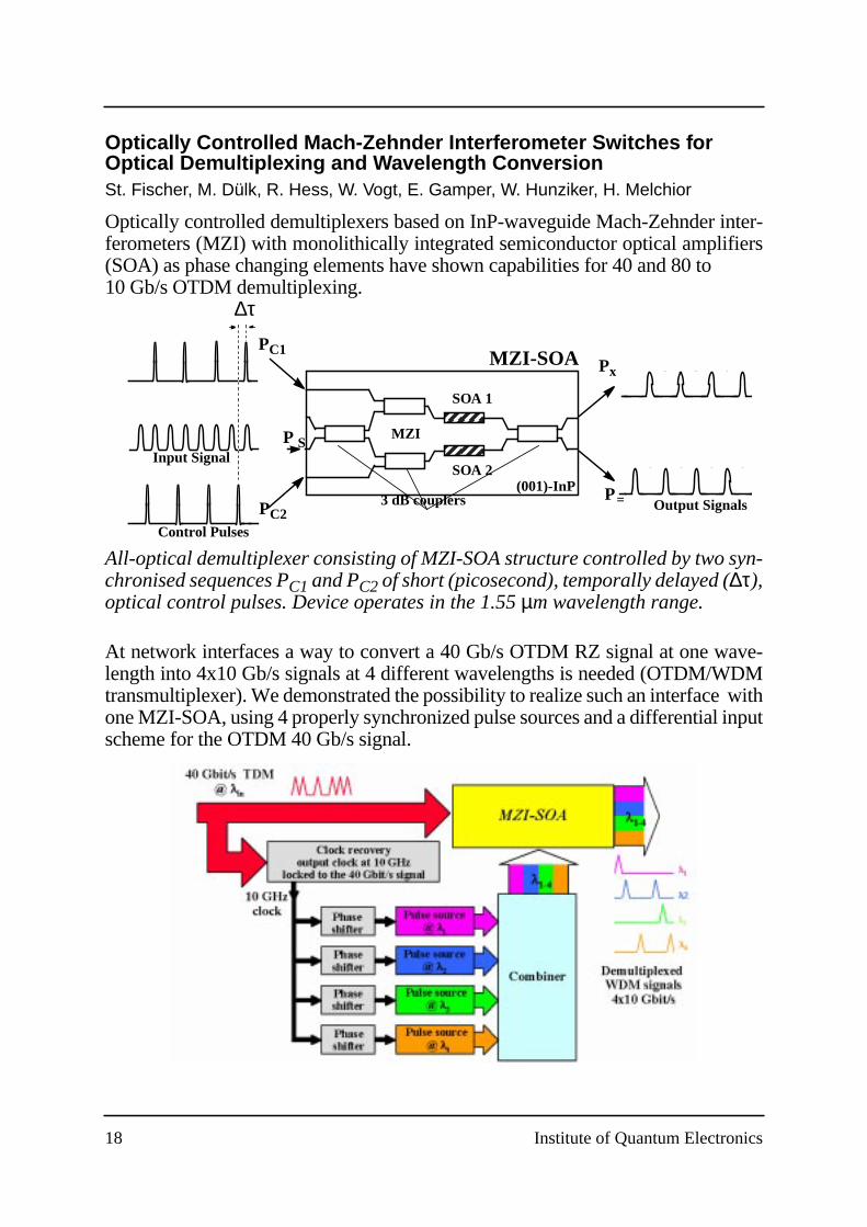
Optically Controlled Mach-Zehnder Interferometer Switches forOptical Demultiplexing and Wavelength Conversion 0.6St. Fischer, M. Dülk, R. Hess, W. Vogt, E. Gamper, W. Hunziker, H. Melchior
Optically controlled demultiplexers based on InP-waveguide Mach-Zehnder iferometers (MZI) with monolithically integrated semiconductor optical amplifi(SOA) as phase changing elements have shown capabilities for 40 and 80 to10 Gb/s OTDM demultiplexing.
All-optical demultiplexer consisting of MZI-SOA structure controlled by two schronised sequences PC1and PC2of short (picosecond), temporally delayed (∆τ),optical control pulses. Device operates in the 1.55µm wavelength range.
At network interfaces a way to convert a 40 Gb/s OTDM RZ signal at one walength into 4x10 Gb/s signals at 4 different wavelengths is needed (OTDM/Wtransmultiplexer). We demonstrated the possibility to realize such an interfaceone MZI-SOA, using 4 properly synchronized pulse sources and a differential ischeme for the OTDM 40 Gb/s signal.
Px
P=PC2
P S
SOA 1
SOA 2(001)-InP
3 dB couplers
MZI
PC1
∆τ
Input Signal
Control Pulses
Output Signals
MZI-SOA
18 Institute of Quantum Electronics
Microelectronics & Optoelectronics Laboratory 19
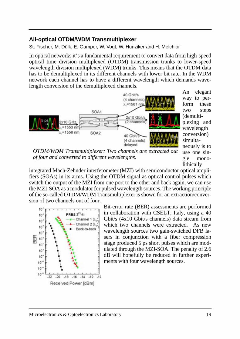
All-optical OTDM/WDM Transmultiplexer 0.1St. Fischer, M. Dülk, E. Gamper, W. Vogt, W. Hunziker and H. Melchior
In optical networks it’s a fundamental requirement to convert data from high-speedoptical time division multiplexed (OTDM) transmission trunks to lower-speedwavelength division multiplexed (WDM) trunks. This means that the OTDM datahas to be demultiplexed in its different channels with lower bit rate. In the WDMnetwork each channel has to have a different wavelength which demands wave-length conversion of the demultiplexed channels.
An elegantway to per-form thesetwo steps(demulti-plexing andwavelengthconversion)simulta-neously is touse one sin-gle mono-lithically
integrated Mach-Zehnder interferometer (MZI) with semiconductor optical ampli-fiers (SOAs) in its arms. Using the OTDM signal as optical control pulses whichswitch the output of the MZI from one port to the other and back again, we can usethe MZI-SOA as a modulator for pulsed wavelength sources. The working principleof the so-called OTDM/WDM Transmultiplexer is shown for an extraction/conver-sion of two channels out of four.
Bit-error rate (BER) assessments are performedin collaboration with CSELT, Italy, using a 40Gbit/s (4x10 Gbit/s channels) data stream fromwhich two channels were extracted. As newwavelength sources two gain-switched DFB la-sers in conjunction with a fiber compressionstage produced 5 ps short pulses which are mod-ulated through the MZI-SOA. The penalty of 2.6dB will hopefully be reduced in further experi-ments with four wavelength sources.
OTDM/WDM Transmultiplexer: Two channels are extracted outof four and converted to different wavelengths.
es orof thehe fu-datadata.n two
ing,ded to
or-
pti-at its
-r
-y
All-Optical Signal Regeneration 0.7St. Fischer, M. Dülk, H. Melchior
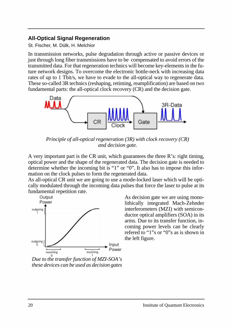
In transmission networks, pulse degradation through active or passive devicjust through long fiber transmissions have to be compensated to avoid errorstransmitted data. For that regeneration technics will become key-elements in tture network designs. To overcome the electronic bottle-neck with increasingrates of up to 1 Tbit/s, we have to evade to the all-optical way to regenerateThese so-called 3R technics (reshaping, retiming, reamplification) are based ofundamental parts: the all-optical clock recovery (CR) and the decision gate.
A very important part is the CR unit, which guarantees the three R’s: right timoptical power and the shape of the regenerated data. The decision gate is needetermine whether the incoming bit is “1” or “0”. It also has to impose this infmation on the clock pulses to form the regenerated data.As all-optical CR unit we are going to use a mode-locked laser which will be ocally modulated through the incoming data pulses that force the laser to pulsefundamental repetition rate.
As decision gate we are using monolithically integrated Mach-Zehndeinterferometers (MZI) with semicon-ductor optical amplifiers (SOA) in itsarms. Due to its transfer function, incoming power levels can be clearlrefered to “1”s or “0”s as is shown inthe left figure.
Principle of all-optical regeneration (3R) with clock recovery (CR)and decision gate.
Due to the transfer function of MZI-SOA’sthese devices can be used as decision gates
20 Institute of Quantum Electronics
hkeyO-ande theen-theandaveen-
y atith
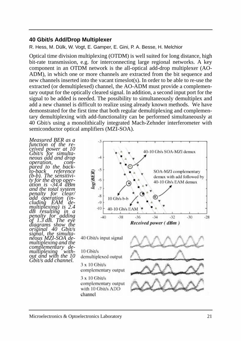
40 Gbit/s Add/Drop Multiplexer 0.8R. Hess, M. Dülk, W. Vogt, E. Gamper, E. Gini, P. A. Besse, H. Melchior
Optical time division multiplexing (OTDM) is well suited for long distance, higbit-rate transmission, e.g. for interconnecting large regional networks. Acomponent in an OTDM network is the all-optical add-drop multiplexer (AADM), in which one or more channels are extracted from the bit sequencenew channels inserted into the vacant timeslot(s). In order to be able to re-usextracted (or demultiplexed) channel, the AO-ADM must provide a complemtary output for the optically cleared signal. In addition, a second input port forsignal to be added is needed. The possibility to simultaneously demultiplexadd a new channel is difficult to realize using already known methods. We hdemonstrated for the first time that both regular demultiplexing and complemtary demultiplexing with add-functionality can be performed simultaneousl40 Gbit/s using a monolithically integrated Mach-Zehnder interferometer wsemiconductor optical amplifiers (MZI-SOA).
Measured BER as afunction of the re-ceived power at 10Gbit/s for simulta-neous add and dropoperation, com-pared to the back-to-back reference(b-b). The sensitivi-ty for the drop oper-ation is -34.4 dBmand the total systempenalty for clear/add operation (in-cluding EAM de-multiplexing) is 2.4dB resulting in apenalty for addingof 1.3 dB. The eyediagrams show theoriginal 40 Gbit/ssignal, the simulta-neous MZI-SOA de-multiplexing and thecomplementary de-multiplexing with-out and with the 10Gbit/s add channel.
0.90.100.11
Microelectronics & Optoelectronics Laboratory 21

callyam-E),
of thethe
and
ZI-per-
Modeling of All-Optical Mach-Zehnder Interferometer Switches 0.12M. Caraccia-Gross, R. Hess, M. Bitter, H. Melchior
A model has been developed to describe all-optical operations of monolithiintegrated Mach-Zehnder interferometers (MZI) with semiconductor opticalplifiers (SOA’s) in their arms. It includes amplified spontaneous emission (ASas well as gain compression and wavelength dependence of the gain andASE. The propagation of the data (d) and of the control (c) signals throughSOA’s is calculated with the help of the following rate equations for the powerfor the phase:
where is the linear gain written with the help of the cubic formula:
For the ASE power we have the following equation
And to complete the model we have the carrier rate equation:
With this model we have simulated pump-probe experiments realized on MSOA’s with 1ps sech2 pulses at 1530 nm wavelength. The simulated and the eximental gating windows conform quite accurately (see figure).
Simulated (sim) and experimental(exp) outputs P= and Px of opticallycontrolled MZI-SOA switch.
∂Pd c,∂z
-------------1vg-----
∂Pd c,∂t
-------------+Γgl N λd c,,( )
1 εch εshb+( )Ptot+----------------------------------------------- αint–
Pd c,=
∂φd c,∂z
-------------1vg-----
∂φd c,∂t
-------------+ 12--- αN αchεch αshbεshb+( )– Ptot[ ]Γgl N λd c,,( )–=
gl N λ,( )
gl N λ,( ) a N Ntr–( ) γ1 λ λN–( )2– γ2 λ λN–( )3 λN,+ λtr χ0 N Ntr–( )–= =
∂Psp± λ( )∂z
-------------------- 1vg-----±
∂Psp± λ( )∂t
--------------------Γgl N λ,( )
1 εch εshb+( )Ptot+----------------------------------------------- αint–
Psp± λ( ) Γ
βsp
2-------BN
2hωλwd+=
∂N∂t------- I
qV------- R N( )–
1hωλi
wd-------------------
Γgl N λi,( )Pi
1 εch εshb+( )Ptot+----------------------------------------------- 1
hωλwd------------------
Γgl N λ,( ) Psp+ λ( ) Psp
- λ( )+( )1 εch εshb+( )Ptot+
---------------------------------------------------------------------λ∑–
i d c,=∑–=
figure in‘~\graphics_melchior\figur1_caraccia.ps’,92mmx62mm
22 Institute of Quantum Electronics
eedplex-for
fig-ductornceinte-
n us-us-
ides,ps ofusedtrical
willther-andl net-
fin-lifiers
Fabrication of All Optical Switches 0.13E. Gamper, W. Vogt, E. Gini
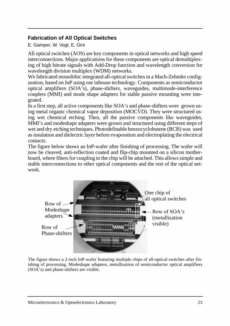
All optical switches (AOS) are key components in optical networks and high spinterconnections. Major applications for these components are optical demultiing of high bitrate signals with Add-Drop function and wavelength conversionwavelength division multiplex (WDM) networks.We fabricated monolithic integrated all-optical switches in a Mach-Zehnder conuration, based on InP using our inhouse technology. Components as semiconoptical amplifiers (SOA’s), phase-shifters, waveguides, multimode-interferecouplers (MMI) and mode shape adapters for stable passive mounting weregrated.In a first step, all active components like SOA’s and phase-shifters were growing metal organic chemical vapor deposition (MOCVD). They were structureding wet chemical etching. Then, all the passive components like waveguMMI’s and modeshape adapters were grown and structured using different stewet and dry etching techniques. Photodefinable benzocyclobutene (BCB) wasas insulation and dielectric layer before evaporation and electroplating the eleccontacts.The figure below shows an InP-wafer after finishing of processing. The wafernow be cleaved, anti-reflection coated and flip-chip mounted on a silicon moboard, where fibers for coupling to the chip will be attached. This allows simplestable interconnections to other optical components and the rest of the opticawork.
The figure shows a 2-inch InP-wafer featuring multiple chips of all-optical switches afterishing of processing. Modeshape adapters, metallization of semiconductor optical amp(SOA’s) and phase-shifters are visible.
Row of SOA’s
Row ofModeshapeadapters (metallization
visible)Row ofPhase-shifters
One chip ofall optical switches
Microelectronics & Optoelectronics Laboratory 23
24 Institute of Quantum Electronics
Principle of Flip-Chip-Mounted All-Optical-Switches 0.1W. Vogt, E. Gamper
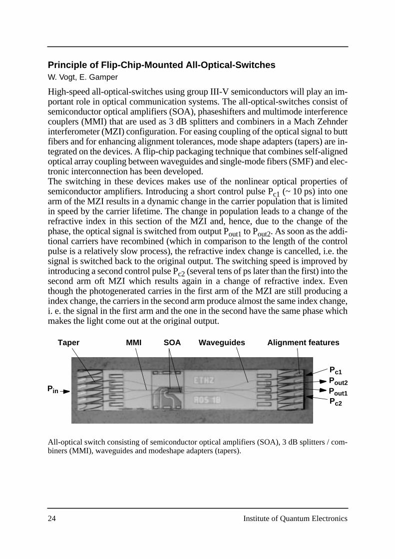
High-speed all-optical-switches using group III-V semiconductors will play an im-portant role in optical communication systems. The all-optical-switches consist ofsemiconductor optical amplifiers (SOA), phaseshifters and multimode interferencecouplers (MMI) that are used as 3 dB splitters and combiners in a Mach Zehnderinterferometer (MZI) configuration. For easing coupling of the optical signal to buttfibers and for enhancing alignment tolerances, mode shape adapters (tapers) are in-tegrated on the devices. A flip-chip packaging technique that combines self-alignedoptical array coupling between waveguides and single-mode fibers (SMF) and elec-tronic interconnection has been developed.The switching in these devices makes use of the nonlinear optical properties ofsemiconductor amplifiers. Introducing a short control pulse Pc1 (~ 10 ps) into onearm of the MZI results in a dynamic change in the carrier population that is limitedin speed by the carrier lifetime. The change in population leads to a change of therefractive index in this section of the MZI and, hence, due to the change of thephase, the optical signal is switched from output Pout1to Pout2. As soon as the addi-tional carriers have recombined (which in comparison to the length of the controlpulse is a relatively slow process), the refractive index change is cancelled, i.e. thesignal is switched back to the original output. The switching speed is improved byintroducing a second control pulse Pc2(several tens of ps later than the first) into thesecond arm oft MZI which results again in a change of refractive index. Eventhough the photogenerated carries in the first arm of the MZI are still producing aindex change, the carriers in the second arm produce almost the same index change,i. e. the signal in the first arm and the one in the second have the same phase whichmakes the light come out at the original output.
All-optical switch consisting of semiconductor optical amplifiers (SOA), 3 dB splitters / com-biners (MMI), waveguides and modeshape adapters (tapers).
Taper MMI SOA Waveguides Alignment features
Pin
Pc1
Pc2
Pout1
Pout2

h-As)
ntrolin thesame
ara-sses,s.OAs
di-
arm
nal
to-epa-
d
bar
Cascadable MZI All-Optical Switch with a Data- and Control-SignalSeparation Scheme 0.14J. Leuthold, P.A. Besse, E. Gamper, M. Dülk, W. Vogt and H. Melchior
All-optically controlled devices in compact monolithically integrated Mach-Zender interferometer configurations with semiconductor optical amplifiers (SOon their arms, have already performed impressive switching speeds.We have realized new types of all-optical devices that allow to separate the coand data signal after signal processing. These new devices allow operationfast copropagating operation mode (control and data signal propagate in thedirection) without additional external wavelength filters for control signal seption at the output. This is advantageous, since external filters introduce lomodify the pulse form of short signals, lack of integration and increase costThe configuration allowing control- and data-signal separation (Fig.) uses 4 S(SOA1 to 4). These form three MZIs: an exterior-MZI (1:2 - 3:4) with two adtional MZIs (1 - 2) and (3 - 4) on each arm of the exterior MZI. Aπ phase shift,inserted either in the upper or the lower branch of the additional MZIs on the(1 - 2) and (3 - 4), respectively, guarantees that both the control (PC1andPC2) andthe input-signal (Pin) are mapped into their respective bar output ports. A sigPin is mapped into the cross outputPX when none of the control signalsPC1 andPC2 are applied. When control signals are applied, the input-signalPin is directedfrom the cross into the bar outputP=. The data and control signals propagategether through the SOAs, but before and behind the MMI couplers they are srated. Crosstalk in undesired channels is below -24 dB.
0.15
PC2
Pin P=
PX
PC1
40:60
SOA1
SOA2
∆φ=π
∆φ=π/2 50:50
SOA4
SOA3
∆φ=π
50:50
50:50
50:50
50:50
Fig. Interleaved MZI all-optical device, with a mode-separation scheme between input ancontrol signal based on the integration of additional MZIs. These additional MZIs(formed by SOA 1-2 and SOA 3-4) are placed on the arms of the exterior MZI. Thephases are adapted to map the control signal and the data signal to their respectiveoutputs.
Microelectronics & Optoelectronics Laboratory 25
racti-rout-Mach-hing,om-lysed
h-Ze-s and
asingg itsg the
t andffectsInP/
ls ofnge.tions
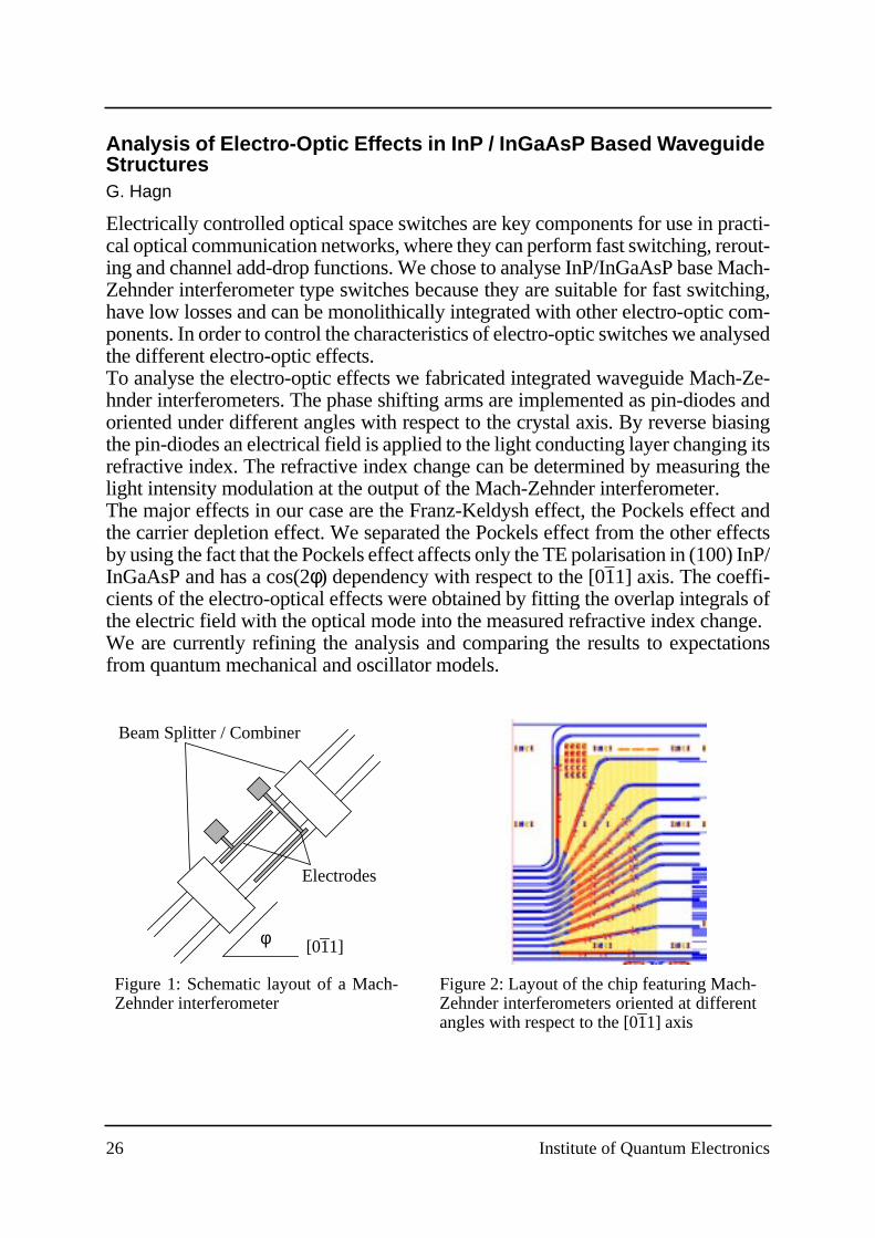
Analysis of Electro-Optic Effects in InP / InGaAsP Based WaveguideStructures 0.16G. Hagn
Electrically controlled optical space switches are key components for use in pcal optical communication networks, where they can perform fast switching, reing and channel add-drop functions. We chose to analyse InP/InGaAsP baseZehnder interferometer type switches because they are suitable for fast switchave low losses and can be monolithically integrated with other electro-optic cponents. In order to control the characteristics of electro-optic switches we anathe different electro-optic effects.To analyse the electro-optic effects we fabricated integrated waveguide Machnder interferometers. The phase shifting arms are implemented as pin-diodeoriented under different angles with respect to the crystal axis. By reverse bithe pin-diodes an electrical field is applied to the light conducting layer changinrefractive index. The refractive index change can be determined by measurinlight intensity modulation at the output of the Mach-Zehnder interferometer.The major effects in our case are the Franz-Keldysh effect, the Pockels effecthe carrier depletion effect. We separated the Pockels effect from the other eby using the fact that the Pockels effect affects only the TE polarisation in (100)InGaAsP and has a cos(2φ) dependency with respect to the [011] axis. The coeffi-cients of the electro-optical effects were obtained by fitting the overlap integrathe electric field with the optical mode into the measured refractive index chaWe are currently refining the analysis and comparing the results to expectafrom quantum mechanical and oscillator models.
Figure 1: Schematic layout of a Mach-Zehnder interferometer
Figure 2: Layout of the chip featuring Mach-Zehnder interferometers oriented at differentangles with respect to the [011] axis
Beam Splitter / Combiner
Electrodes
φ [011]
26 Institute of Quantum Electronics
Microelectronics & Optoelectronics Laboratory 27
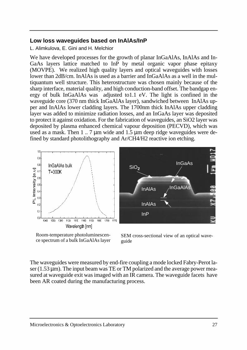
Low loss waveguides based on InAlAs/InP 0.1L. Alimkulova, E. Gini and H. Melchior
We have developed processes for the growth of planar InGaAlAs, InAlAs and In-GaAs layers lattice matched to InP by metal organic vapor phase epitaxy(MOVPE). We realized high quality layers and optical waveguides with losseslower than 2dB/cm. InAlAs is used as a barrier and InGaAlAs as a well in the mul-tiquantum well structure. This heterostructure was chosen mainly because of thesharp interface, material quality, and high conduction-band offset. The bandgap en-ergy of bulk InGaAlAs was adjusted to1.1 eV. The light is confined in thewaveguide core (370 nm thick InGaAlAs layer), sandwiched between InAlAs up-per and InAlAs lower cladding layers. The 1700nm thick InAlAs upper claddinglayer was added to minimize radiation losses, and an InGaAs layer was depositedto protect it against oxidation. For the fabrication of waveguides, an SiO2 layer wasdeposited by plasma enhanced chemical vapour deposition (PECVD), which wasused as a mask. Then 1 .. 7µm wide and 1.5µm deep ridge waveguides were de-fined by standard photolithography and Ar/CH4/H2 reactive ion etching.
The waveguides were measured by end-fire coupling a mode locked Fabry-Perot la-ser (1.53µm). The input beam was TE or TM polarized and the average power mea-sured at waveguide exit was imaged with an IR camera. The waveguide facets havebeen AR coated during the manufacturing process.
InAlAs
InAlAs
InGaAlAs
InP
SiO2InGaAs
Room-temperature photoluminescen-ce spectrum of a bulk InGaAlAs layer
SEM cross-sectional view of an optical wave-guide
posespticalene-pulse
syn-0 psto 50
-lock-ode
laserslargeode-s, toaggode-
High Bit Rate Optical Pulse Sources
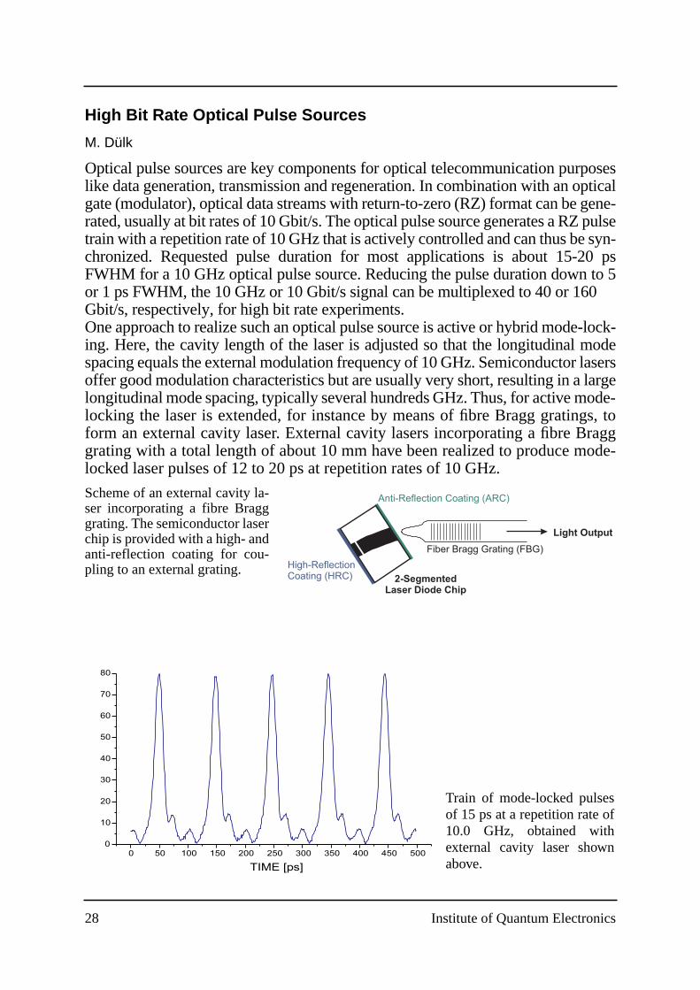
M. Dülk
Optical pulse sources are key components for optical telecommunication purlike data generation, transmission and regeneration. In combination with an ogate (modulator), optical data streams with return-to-zero (RZ) format can be grated, usually at bit rates of 10 Gbit/s. The optical pulse source generates a RZtrain with a repetition rate of 10 GHz that is actively controlled and can thus bechronized. Requested pulse duration for most applications is about 15-2FWHM for a 10 GHz optical pulse source. Reducing the pulse duration downor 1 ps FWHM, the 10 GHz or 10 Gbit/s signal can be multiplexed to 40 or 16Gbit/s, respectively, for high bit rate experiments.One approach to realize such an optical pulse source is active or hybrid modeing. Here, the cavity length of the laser is adjusted so that the longitudinal mspacing equals the external modulation frequency of 10 GHz. Semiconductoroffer good modulation characteristics but are usually very short, resulting in alongitudinal mode spacing, typically several hundreds GHz. Thus, for active mlocking the laser is extended, for instance by means of fibre Bragg gratingform an external cavity laser. External cavity lasers incorporating a fibre Brgrating with a total length of about 10 mm have been realized to produce mlocked laser pulses of 12 to 20 ps at repetition rates of 10 GHz.
High-ReflectionCoating (HRC)
Fiber Bragg Grating (FBG)
Anti-Reflection Coating (ARC)
2-SegmentedLaser Diode Chip
Light Output
Scheme of an external cavity la-ser incorporating a fibre Bragggrating. The semiconductor laserchip is provided with a high- andanti-reflection coating for cou-pling to an external grating.
0 50 100 150 200 250 300 350 400 450 500
0
10
20
30
40
50
60
70
80
TIME [ps]
Train of mode-locked pulsesof 15 ps at a repetition rate of10.0 GHz, obtained withexternal cavity laser shownabove.
28 Institute of Quantum Electronics

n-lti-
guide’s.sta-ease
Wavelength Multiplexer Modules in Glass on Silicon 0.17Ch. Nadler, W. Hunziker, E. Wildermuth and M. Lanker
Wavelength division multiplexing (WDM) offers full exploitation of the almost ulimited bandwidths of optical fibers. Key elements of WDM are wavelength muplexers (WMUX’s).
For an optical packet switching and routing network we used the arrayed wavegrating (AWG) concept and the silica on silicon technology to realize WMUXThis allows for low-loss, low-crosstalk, exact channel allocation, and long termbility. A penalty-free birefringence compensation method using stress relgrooves reduces the fabrication induced strain birefringence.
Fully packaged 16 channelwavelength multiplexer mod-ule with opened case and mea-sured performance data. Input fiber
WMUX Chip
Output Fibers
νITU ν20 νextr. 50[THz] [THz] [THz]
195.30 195.36 195.31195.10 195.16 195.11... ... ...193.50 193.55 193.50193.30 193.35 193.30193.10 193.15 193.10192.90 192.95 192.90192.70 192.75 192.70192.50 192.55 192.51192.30 192.36 192.31
Number of Channels: 16Material and Index Contrast: SiO 2/Si , 0.7%Center Frequency: 193.75 THz (1547.4 nm)Channel Spacing: 200 GHz (1.60 nm)Fiber-to-Fiber-Insertion Loss: < 5.2 dBOptical Crosstalk: < -25 dBFree Spectral Range: > 27 nm
3 dB Filter bandwidth: 0.5 nmChip Size: 70 mm x 23 mmPolarization shift: < 0.04 nmPolarization penalty: < 0.2 dBTemperature dependence: 1.25 GHz/ °CITU Grid reached at: 50 °CTransmission measured at: 20 °C
Microelectronics & Optoelectronics Laboratory 29
tion.such
ct de-. am-
ndente in-ses,ossi-mec-
s anddexr ef-enceture.
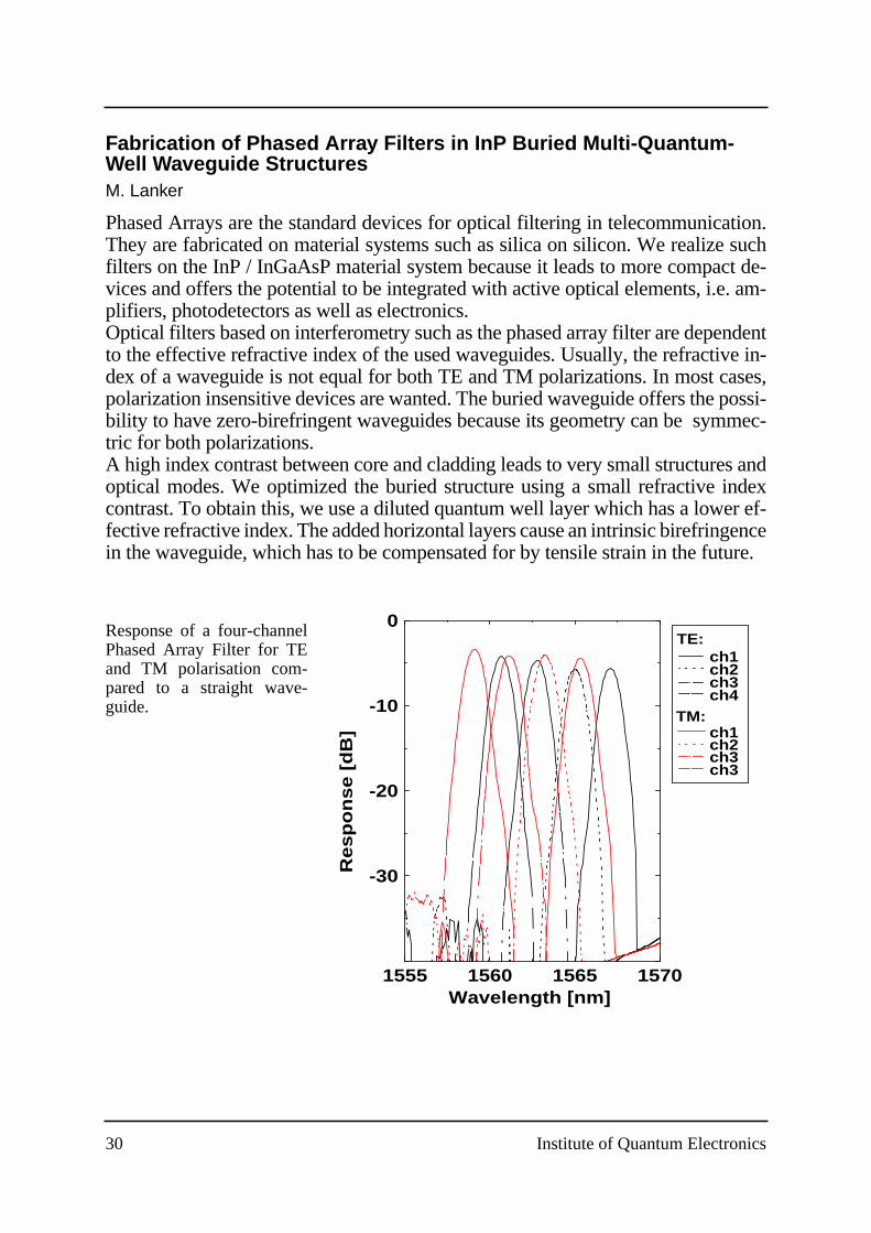
Fabrication of Phased Array Filters in InP Buried Multi-Quantum-Well Waveguide Structures 0.18M. Lanker
Phased Arrays are the standard devices for optical filtering in telecommunicaThey are fabricated on material systems such as silica on silicon. We realizefilters on the InP / InGaAsP material system because it leads to more compavices and offers the potential to be integrated with active optical elements, i.eplifiers, photodetectors as well as electronics.Optical filters based on interferometry such as the phased array filter are depeto the effective refractive index of the used waveguides. Usually, the refractivdex of a waveguide is not equal for both TE and TM polarizations. In most capolarization insensitive devices are wanted. The buried waveguide offers the pbility to have zero-birefringent waveguides because its geometry can be symtric for both polarizations.A high index contrast between core and cladding leads to very small structureoptical modes. We optimized the buried structure using a small refractive incontrast. To obtain this, we use a diluted quantum well layer which has a lowefective refractive index. The added horizontal layers cause an intrinsic birefringin the waveguide, which has to be compensated for by tensile strain in the fu
Response of a four-channelPhased Array Filter for TEand TM polarisation com-pared to a straight wave-guide.
1555 1560 1565 1570
-30
-20
-10
0
ch1ch2ch3ch4
ch1ch2ch3
TM:
TE:
ch3
Re
spo
nse
[d
B]
Wavelength [nm]
30 Institute of Quantum Electronics
In-ips.bot-ct re-s ares (asrfacepinandub-pho-um
e tos ared withht ab-lting
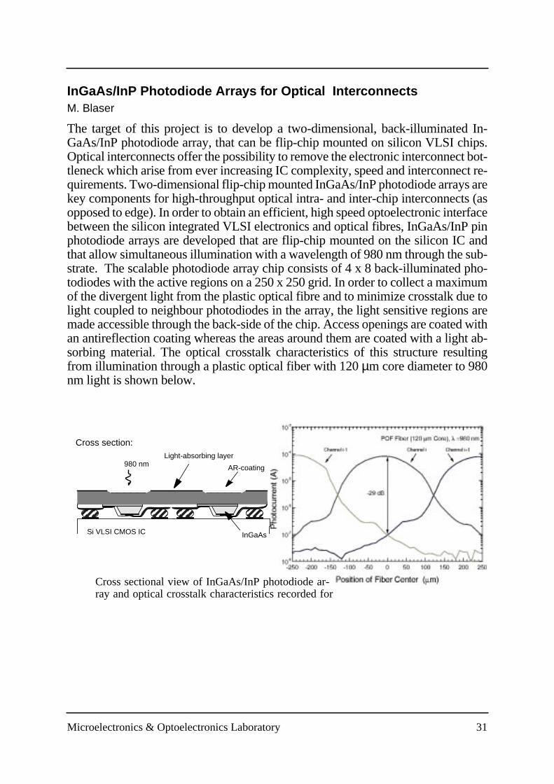
InGaAs/InP Photodiode Arrays for Optical Interconnects 0.19M. Blaser
The target of this project is to develop a two-dimensional, back-illuminatedGaAs/InP photodiode array, that can be flip-chip mounted on silicon VLSI chOptical interconnects offer the possibility to remove the electronic interconnecttleneck which arise from ever increasing IC complexity, speed and interconnequirements. Two-dimensional flip-chip mounted InGaAs/InP photodiode arraykey components for high-throughput optical intra- and inter-chip interconnectopposed to edge). In order to obtain an efficient, high speed optoelectronic intebetween the silicon integrated VLSI electronics and optical fibres, InGaAs/InPphotodiode arrays are developed that are flip-chip mounted on the silicon ICthat allow simultaneous illumination with a wavelength of 980 nm through the sstrate. The scalable photodiode array chip consists of 4 x 8 back-illuminatedtodiodes with the active regions on a 250 x 250 grid. In order to collect a maximof the divergent light from the plastic optical fibre and to minimize crosstalk dulight coupled to neighbour photodiodes in the array, the light sensitive regionmade accessible through the back-side of the chip. Access openings are coatean antireflection coating whereas the areas around them are coated with a ligsorbing material. The optical crosstalk characteristics of this structure resufrom illumination through a plastic optical fiber with 120µm core diameter to 980nm light is shown below.
Si VLSI CMOS IC
Light-absorbing layer
AR-coating
InGaAs
980 nm
Cross section:
Cross sectional view of InGaAs/InP photodiode ar-ray and optical crosstalk characteristics recorded for
Microelectronics & Optoelectronics Laboratory 31
veddards
ical) andan-tron
eter-radi-osurenmcoun-ty by
rders in
i-d
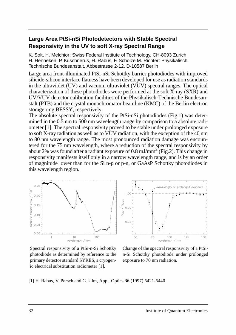
Large Area PtSi-nSi Photodetectors with Stable SpectralResponsivity in the UV to soft X-ray Spectral Range
K. Solt, H. Melchior: Swiss Federal Institute of Technology, CH-8093 ZurichH. Henneken, P. Kuschnerus, H. Rabus, F. Scholze M. Richter: PhysikalischTechnische Bundesanstalt, Abbestrasse 2-12, D-10587 Berlin
Large area front-illuminated PtSi-nSi Schottky barrier photodiodes with improsilicide-silicon interface flatness have been developed for use as radiation stanin the ultraviolet (UV) and vacuum ultraviolet (VUV) spectral ranges. The optcharacterization of these photodiodes were performed at the soft X-ray (SXRUV/VUV detector calibration facilities of the Physikalisch-Technische Bundesstalt (PTB) and the crystal monochromator beamline (KMC) of the Berlin elecstorage ring BESSY, respectively.The absolute spectral responsivity of the PtSi-nSi photodiodes (Fig.1) was dmined in the 0.5 nm to 500 nm wavelength range by comparison to a absoluteometer [1]. The spectral responsivity proved to be stable under prolonged expto soft X-ray radiation as well as to VUV radiation, with the exception of the 40to 80 nm wavelength range. The most pronounced radiation damage was entered for the 75 nm wavelength, where a reduction of the spectral responsiviabout 2% was found after a radiant exposure of 0.8 mJ/mm2 (Fig.2). This change inresponsivity manifests itself only in a narrow wavelength range, and is by an oof magnitude lower than for the Si n-p or p-n, or GaAsP Schottky photodiodethis wavelength region.
[1] H. Rabus, V. Persch and G. Ulm, Appl. Optics36 (1997) 5421-5440
0.20
Change of the spectral responsivity of a PtSn-Si Schottky photodiode under prolongeexposure to 70 nm radiation.
Spectral responsivity of a PtSi-n-Si Schottkyphotodiode as determined by reference to theprimary detector standard SYRES, a cryogen-ic electrical substitution radiometer [1].
32 Institute of Quantum Electronics
Microelectronics & Optoelectronics Laboratory 33
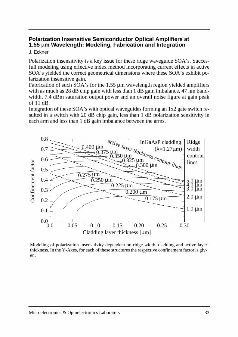
Polarization Insensitive Semiconductor Optical Amplifiers at1.55 µm Wavelength: Modeling, Fabrication and Integration 0.1J. Eckner
Polarization insensitivity is a key issue for these ridge waveguide SOA’s. Succes-full modeling using effective index method incorporating current effects in activeSOA’s yielded the correct geometrical dimensions where these SOA’s exhibit po-larization insensitive gain.Fabrication of such SOA’s for the 1.55µm wavelength region yielded amplifierswith as much as 28 dB chip gain with less than 1 dB gain imbalance, 47 nm band-width, 7.4 dBm saturation output power and an overall noise figure at gain peakof 11 dB.Integration of these SOA’s with optical waveguides forming an 1x2 gate switch re-sulted in a switch with 20 dB chip gain, less than 1 dB polarization sensitivity ineach arm and less than 1 dB gain imbalance between the arms.
Cladding Layer Thickness [µm]
Con
finem
ent F
acto
r
0.00 0.05 0.10 0.15 0.20 0.25 0.300.00
0.10
0.20
0.30
0.40
0.50
0.60
0.70
0.80
0.175µm0.200µm
0.225µm0.250µm
0.300µm0.325µm
0.350µm0.375µm
0.400µmactive layer thickness contour lines
Ridge width contour lines
5.0µm4.0µm3.0µm
2.0µm
1.0µm
InGaAsP cladding(λ=1.27µm)
0.275µm
0.0 0.05 0.10 0.15 0.20 0.25 0.30Cladding layer thickness [µm]
Con
finem
ent f
acto
r
0.8
0.7
0.6
0.5
0.4
0.3
0.2
0.1
0.0
Modeling of polarization insensitivity dependent on ridge width, cladding and active layerthickness. In the Y-Axes, for each of these structures the respective confinement factor is giv-en.

igh-igh-
ready
1 -1]
usingtionthef the
l alleasy
f the
beenits forers.
byn
A New Concept for InP HBT Circuit Fabrication Technology 0.21M. Le Pallec
Fabrication process and layout are of major importance for the realization of hspeed InP Heterojunction Bipolar Transistor-based integrated circuits. A hperformance HBT fabrication process using self-aligned techniques has albeen demonstrated at IQE. One of this proven techniques - a self-aligned emitter-base metallization -takes avantage of wet chemical etching profiles in the [0crystal direction of InP and InGaAs.A new submicron HBT-based fabrication process has been investigated by
this wet chemical etching know-how and by exploiting the noticeable planarizaproperties of BCB dielectric. One of the key steps of this technology relies onconnections at the same top level of all components by taking avantage osmooth etching profile of InP and InGaAs in the [0 1 -1] crystal direction (θ=30˚).After spin-on and curing the BCB coating is etched back by RIE to reveacontacts, prior to a thick metallization deposition. This technique enables anconnection of the submicron emitter finger and a substantial reduction oparasitic base-collector capacitance of the base metallization pad.A fast fabrication process for HBT-based integrated circuits (6-7 masks) hasdeveloped on this concept. Its applications include high-speed integrated circuoptical communications over 40 Gbit/s, such as driver circuits and photoreceiv
Lay-out and cross-sectional view in the [0 1 -1] crystal direction of the projected InP-HBTexploiting the BCB planarization properties and the wet chemical etching profile directiodependency of InP and InGaAs.
34 Institute of Quantum Electronics

Microelectronics & Optoelectronics Laboratory 35
Monolithically Integrated 40Gb/s pin/HBT Optical Receiver Module 0.1M. Bitter, R. Bauknecht and W. Hunziker
For future 40Gb/s time-division multiplexed (TDM) fiber-optic transmission sys-tems, high-speed baseband optical receivers are needed. The monolithic integrationof optical receivers offers the advantages of high-speed performance, small size andpossible cost reduction of packaging. Besides a suitable technology for the integra-tion of photodiodes and transistors, a broadband mounting technique is crucial forthe fabrication of optical receiver modules. For the realization of our optical receiv-er module we monolithically integrated top-illuminated pin photodiodes with sin-gle-heterojunction bipolar transistors (HBT) in the InP/InGaAs material system.The optical receiver circuit consists of a pin photodiode and a broadband darlingtonfeedback amplifier. The optical receiver chip is connected to an alumina mountingsubstrate by wire bonding. On this mounting substrate, we integrated the neces-sary decoupling circuitry and bias network for the optical receiver chip. The op-tical receiver chip and alumina mounting substrate are built in a brass housing andfurnished with connectors for the DC power supply and the RF output signal. Aslant-ended single-mode fiber couples the incoming light into the top-illuminatedpin photodiode.At 1550nm wavelength, we measured an overall conversion gain of 48V/W, an op-toelectronic small-signal bandwidth of 30GHz and clearly opened eyes for a 40Gb/s transmission experiment for our optical receiver module.
Photograph of optical receiver module (left) and measured eye-diagram obtained from a trans-mission experiment at 40Gb/s (right). The optical signal was an RZ coded PRBS with a se-quence length of 231-1 and input optical mean power of -1dBm at a wavelength of 1550nm.
Time: 10ps/div
Out
put V
olta
ge: 2
0mV
/div
Fiber pig-tail
RF out
le tosemi-
pre-penthat
cur-
dardcoax-st. Forto theg in a
.4 Wown
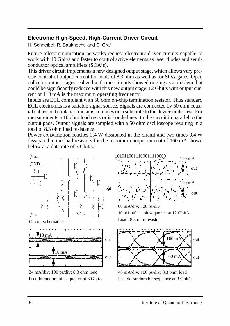
Electronic High-Speed, High-Current Driver Circuit 0.22H. Schneibel, R. Bauknecht, and C. Graf
Future telecommunication networks request electronic driver circuits capabwork with 10 Gbit/s and faster to control active elements as laser diodes andconductor optical amplifiers (SOA’s).This driver circuit implements a new designed output stage, which allows verycise control of output current for loads of 8.3 ohm as well as for SOA-gates. Ocollector output stages realized in former circuits showed ringing as a problemcould be significantly reduced with this new output stage. 12 Gbit/s with outputrent of 110 mA is the maximum operating frequency.Inputs are ECL compliant with 50 ohm on-chip termination resistor. Thus stanECL electronics is a suitable signal source. Signals are connected by 50 ohmial cables and coplanar transmission lines on a substrate to the device under temeasurements a 10 ohm load resistor is bonded next to the circuit in paralleloutput pads. Output signals are sampled with a 50 ohm oscilloscope resultintotal of 8.3 ohm load resistance.Power consumption reaches 2.4 W dissipated in the circuit and two times 0dissipated in the load resistors for the maximum output current of 160 mA shbelow at a data rate of 3 Gbit/s.
VPlus
GND
in
VEE VEE2
out
Circuit schematics
48 mA/div; 100 ps/div; 8.3 ohm load
Pseudo random bit sequence at 3 Gbit/s
24 mA/div; 100 ps/div; 8.3 ohm load
Pseudo random bit sequence at 3 Gbit/s
out
out
160 mA
160 mA
18 mA
18 mA
1010110011100011110000
out
out
110 mA
110 mA
out
out
60 mA/div; 500 ps/div
101011001... bit sequence at 12 Gbit/s
Load: 8.3 ohm resistor
36 Institute of Quantum Electronics
sti-CMaced.LSI
andck dis-ips inep-
mentoadsured.tect-Oper-
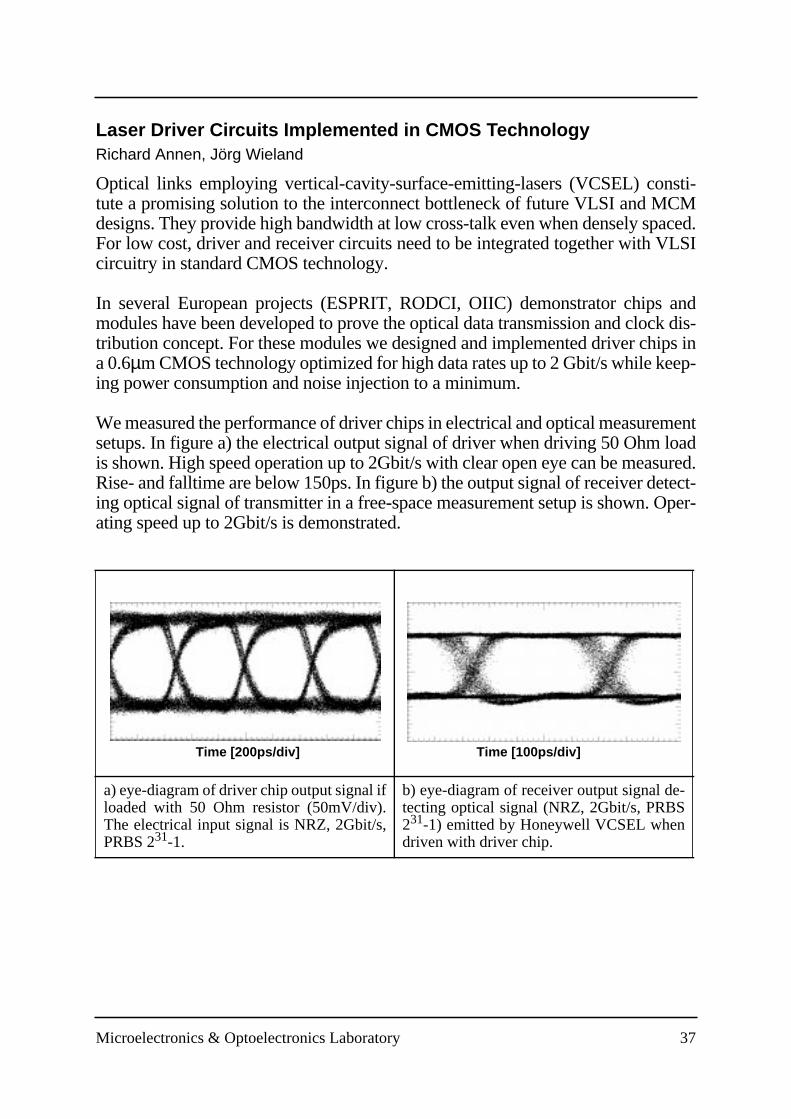
Laser Driver Circuits Implemented in CMOS Technology 0.23Richard Annen, Jörg Wieland
Optical links employing vertical-cavity-surface-emitting-lasers (VCSEL) contute a promising solution to the interconnect bottleneck of future VLSI and Mdesigns. They provide high bandwidth at low cross-talk even when densely spFor low cost, driver and receiver circuits need to be integrated together with Vcircuitry in standard CMOS technology.
In several European projects (ESPRIT, RODCI, OIIC) demonstrator chipsmodules have been developed to prove the optical data transmission and clotribution concept. For these modules we designed and implemented driver cha 0.6µm CMOS technology optimized for high data rates up to 2 Gbit/s while keing power consumption and noise injection to a minimum.
We measured the performance of driver chips in electrical and optical measuresetups. In figure a) the electrical output signal of driver when driving 50 Ohm lis shown. High speed operation up to 2Gbit/s with clear open eye can be meaRise- and falltime are below 150ps. In figure b) the output signal of receiver deing optical signal of transmitter in a free-space measurement setup is shown.ating speed up to 2Gbit/s is demonstrated.
a) eye-diagram of driver chip output signal ifloaded with 50 Ohm resistor (50mV/div).The electrical input signal is NRZ, 2Gbit/s,PRBS 231-1.
b) eye-diagram of receiver output signal de-tecting optical signal (NRZ, 2Gbit/s, PRBS231-1) emitted by Honeywell VCSEL whendriven with driver chip.
Time [200ps/div] Time [100ps/div]
Microelectronics & Optoelectronics Laboratory 37

infor-oardscon-g par-ew,
T, ourand
eng-eceivert dis-verseiversrojectscomeeiv-
anddBmr ca-
rs
to
Receivers for Optical Interconnects 0.24A. Schmid
The increasing amounts of data generated by new emerging multimedia andmation technology services must be transported between and within racks, band integrated circuits of electronic systems. Serial and parallel optical internects are capable of handling this vast amount of data. Reasons for considerinallel optical interconnects include, low latency, minimal delays and sksimplified and less power consuming electronics and compactness.
In the frame of several European research projects, such as OIIC and COBNEgroup has developed AC-coupled parallel receiver arrays in commercial CMOSBiCMOS technologies with aggregate line-bitrates above 10Gbit/s. Main challes in the design of these receiver arrays have been crosstalk suppression, rsensitivity and low power dissipation. The CMOS receivers are suited for shortance interconnects between and within CMOS VLSI ICs. The BiCMOS receiaim at medium distance interconnects between boards and racks. The rechave been implemented with success in the system demonstrators of these pand show that parallel optical interconnects are an attractive solution to overthe bottlenecks of their electrical counterparts. The sensitivity for the CMOS recers is -23.6dBm at a bitrate of 150Mbit/s with a detector responsivity of 1A/Wa detector capacitance of 2pF. The sensitivity for the BiCMOS receiver is -26at a bitrate of 1.06Gbit/s with a detector responsivity of 0.8A/W and a detectopacitance of 0.5pF.
Figure: Left: OIIC 8x8 CMOS receiver array with flip-chip mounted detectobonded onto a ceramic substrate for operation up to 150Mbit/s/cannel.Right: COBNET 12-channel BiCMOS receiver array IC for operation up1.06Gbit/s/channel.
38 Institute of Quantum Electronics
ter-,hput
. Theinput
it/s.
een
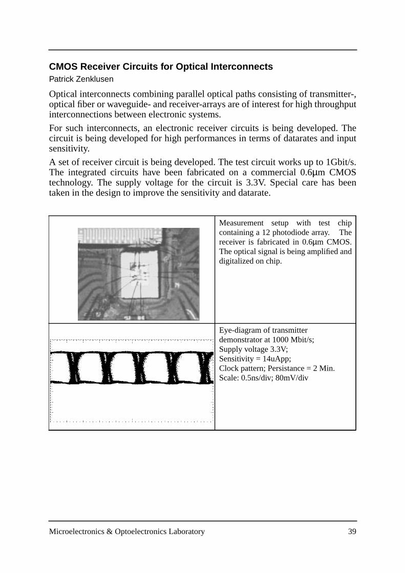
CMOS Receiver Circuits for Optical Interconnects 0.25Patrick Zenklusen
Optical interconnects combining parallel optical paths consisting of transmitoptical fiber or waveguide- and receiver-arrays are of interest for high througinterconnections between electronic systems.
For such interconnects, an electronic receiver circuits is being developedcircuit is being developed for high performances in terms of datarates andsensitivity.
A set of receiver circuit is being developed. The test circuit works up to 1GbThe integrated circuits have been fabricated on a commercial 0.6µm CMOStechnology. The supply voltage for the circuit is 3.3V. Special care has btaken in the design to improve the sensitivity and datarate.
Measurement setup with test chipcontaining a 12 photodiode array. Thereceiver is fabricated in 0.6µm CMOS.The optical signal is being amplified anddigitalized on chip.
Eye-diagram of transmitterdemonstrator at 1000 Mbit/s;Supply voltage 3.3V;Sensitivity = 14uApp;Clock pattern; Persistance = 2 Min.Scale: 0.5ns/div; 80mV/div
Microelectronics & Optoelectronics Laboratory 39
edseffi-bitsPLLsio-
con-nts.ring.e con-g.ce anent aothernd it
MHzs ex-
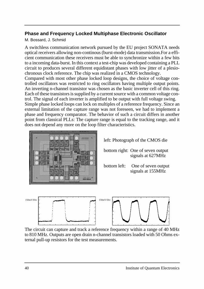
Phase and Frequency Locked Multiphase Electronic Oscillator 0.26M. Bossard, J. Schmid
A switchless communication network pursued by the EU project SONATA neoptical receivers allowing non-continous (burst-mode) data transmission.For acient communication these receivers must be able to synchronize within a fewto a incoming data-burst. In this context a test-chip was developed containing acircuit to produces several different equidistant phases with low jitter of a plechronous clock reference. The chip was realized in a CMOS technology.Compared with most other phase locked loop designs, the choice of voltagetrolled oscillators was restricted to ring oscillators having multiple output poiAn inverting n-channel transistor was chosen as the basic inverter cell of thisEach of these transistors is supplied by a current source with a common voltagtrol. The signal of each inverter is amplified to be output with full voltage swinSimple phase locked loops can lock on multiples of a reference frequency. Sinexternal limitation of the capture range was not foreseen, we had to implemphase and frequency comparator. The behavior of such a circuit differs in anpoint from classical PLLs: The capture range is equal to the tracking range, adoes not depend any more on the loop filter characteristics.
left: Photograph of the CMOS die
bottom right: One of seven outputsignals at 627MHz
bottom left: One of seven outputsignals at 155MHz
The circuit can capture and track a reference frequency within a range of 40to 810 MHz. Outputs are open drain n-channel transistors loaded with 50 Ohmternal pull-up resistors for the test measurements.
150mV/Div150mV/Div
40 Institute of Quantum Electronics
tendour
. With
tes bitce
mingntse bit-
o fur-
vary.
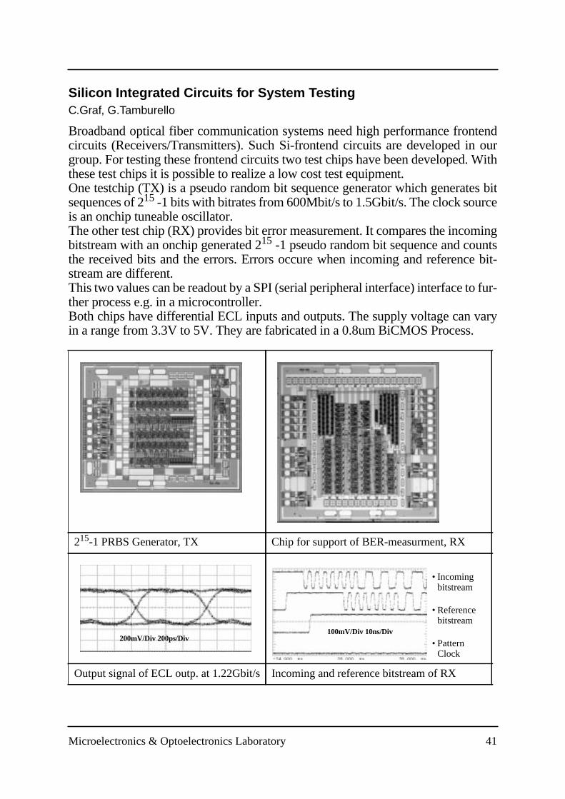
Silicon Integrated Circuits for System Testing 0.27C.Graf, G.Tamburello
Broadband optical fiber communication systems need high performance froncircuits (Receivers/Transmitters). Such Si-frontend circuits are developed ingroup. For testing these frontend circuits two test chips have been developedthese test chips it is possible to realize a low cost test equipment.One testchip (TX) is a pseudo random bit sequence generator which generasequences of 215-1 bits with bitrates from 600Mbit/s to 1.5Gbit/s. The clock souris an onchip tuneable oscillator.The other test chip (RX) provides bit error measurement. It compares the incobitstream with an onchip generated 215 -1 pseudo random bit sequence and couthe received bits and the errors. Errors occure when incoming and referencstream are different.This two values can be readout by a SPI (serial peripheral interface) interface tther process e.g. in a microcontroller.Both chips have differential ECL inputs and outputs. The supply voltage canin a range from 3.3V to 5V. They are fabricated in a 0.8um BiCMOS Process
215-1 PRBS Generator, TX Chip for support of BER-measurment, RX
Output signal of ECL outp. at 1.22Gbit/s Incoming and reference bitstream of RX
200mV/Div 200ps/Div100mV/Div 10ns/Div
• Incomingbitstream
• Referencebitstream
• PatternClock
Microelectronics & Optoelectronics Laboratory 41

l initableitalctro-
arent
of the) for. Weingfunc-
t indevicecom-
ple-
Digital Optical Fibre Logic ModulesL. Occhi, F. Girardin, G. Guekos
All-optical logic and processing of information has a vast application potentiatelecommunications and high-speed signal processing. The exploration of a sutechnology platform to build and exploit the possibilities of using all-optical, diglogic circuits for data processing at rates potentially in excess of those than elenic circuits are capable of is a promising approach towards the optically transpfibre networks and associated diagnostic instrumentation.In co-operation with European partners we are investigating the performanceSagnac interferometer incorporating semiconductor optical amplifiers (SOAswavelengths around 1550 nm as building blocks for all-optical logic operationshave demonstrated the feasibility to construct Sagnac logic gates with switchenergy as low as 10 fJ, latency as low as 13 ns, and have tested the Booleantionality AND, NOT and XOR up to 10 GHz. Since the SOA is the key elementhe Sagnac interferometer, we have tested the gain recovery dynamics of theand found how they depend on device length and optical signal intensity byparing modeling and experimental results. We are now proceeding with the immentation of gate cascadability and frequency up-gradability to 20 GHz.
0 100 200 300 4000
0.2
0.4
0.6
0.8
1
Time (ps)
No
rma
lize
d p
rob
e tra
nsm
issi
on
0 0.2 0.4 0.6 0.850
100
150
200
250
300
350
400
450
500
Probe power (mW)
Ga
in r
eco
ve
ry tim
e (
ps)
(a)
Typical probe transmission curves for 500µm (◊)and 1500µm (+) long SOA devices
Measured 10%-90% gain recovery time for fourdifferent SOA lengths as a function of the inputpower. 500µm (◊); 750µm (); 1000µm (o); and1500µm (+).
42 Institute of Quantum Electronics
mo-use ofeter-ns canom
impleicaltun-This
latorsffect-ingle-
g a
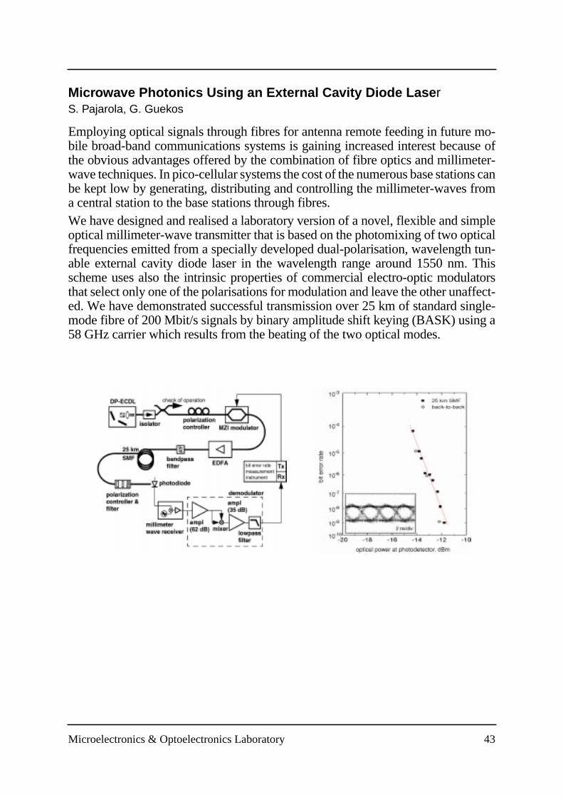
Microwave Photonics Using an External Cavity Diode Lase rS. Pajarola, G. Guekos
Employing optical signals through fibres for antenna remote feeding in futurebile broad-band communications systems is gaining increased interest becathe obvious advantages offered by the combination of fibre optics and millimwave techniques. In pico-cellular systems the cost of the numerous base statiobe kept low by generating, distributing and controlling the millimeter-waves fra central station to the base stations through fibres.We have designed and realised a laboratory version of a novel, flexible and soptical millimeter-wave transmitter that is based on the photomixing of two optfrequencies emitted from a specially developed dual-polarisation, wavelengthable external cavity diode laser in the wavelength range around 1550 nm.scheme uses also the intrinsic properties of commercial electro-optic moduthat select only one of the polarisations for modulation and leave the other unaed. We have demonstrated successful transmission over 25 km of standard smode fibre of 200 Mbit/s signals by binary amplitude shift keying (BASK) usin58 GHz carrier which results from the beating of the two optical modes.
Microelectronics & Optoelectronics Laboratory 43

44 Institute of Quantum Electronics
Semiconductor Optical Amplifiers in Four-Wave Mixing SystemExperimentsF. Girardin, L. Occhi, G. Guekos
Semiconductor Optical Amplifiers (SOAs) designed and fabricated in our group,exhibiting high fibre-to-fibre optical gain around 25 dB, polarisation sensitivity lessthan 2 dB, and having different lengths, were implemented in several fibre-optictransmission system experiments that make use of the Four-Wave Mixing (FWM)effect, in collaboration with research groups at the Fondazione Ugo Bordoni, Rome,the California Institute of Technology, Pasadena, and the company Opto Speed SAin Mezzovico, Ticino. Purpose of the experiments was to prove the suitability of theFWM process to perform wavelength conversion and mid-span spectral inversionunder system conditions that come close to real applications.
The investigations showed for the first time that the full optical bandwidth of thewidely employed erbium-doped fibre amplifiers in modern fibre systems can becovered with wavelength converters based on FWM. The experiments confirmedpractically error-free wavelength conversion ranges of at least 30 nm down- and atleast 15 nm up-conversion for signals at bit rates of 10 Gbit/s.
Mid-span spectral inversion for dispersion compensation was realised in a labora-tory set-up in order to explore the feasibility of the FWM process to upgrade tohigher bit rates the existing networks made of standard single-mode fibres. By usingtwo orthogonal optical pumps at different wavelengths, penalty-free transmissionover 120 km at 2.5 Gbit/s was achieved. By using a similar two-pump scheme,wavelength conversion to both up- and down-wavelengths was realised with effi-ciencies that remain within a few dBs over several THz frequency range.
Pump1
Pump2
Signal
SOA
PD
MonochromatorPDAmplifierLock-In
PC
PC
PC
50%/50%
OI
OI
OI
OI
OI
FP
PDChopper
PC
OI
POL
90%/10%

uan-withysicsainedard-ith
gen-ex-ntalre-setts ins.neersactmu-abo-ore,versi-
Fibreoptic Telecommunications Education in Developing CountriesG. Guekos
The engagement of the Micro- and Optoelectronics Group of the Institute for Qtum Electronics in the cooperation with developing countries started in 1986courses by our co-workers at the International Centre for Theoretical Ph(ICTP) in Trieste. Since then, more than 600 physicists and engineers were trin Trieste and in developing countries following stringent selection criteria reging basic qualifications in the field of modern communication technologies. Wthe financial support from the Swiss Development and Cooperation (DEZA) acy of the Ministry of Foreign Affairs, Berne, we have set-up practical laboratoryperiments at the ICTP and in developing countries aiming at (i) experimeaccompaniment of courses through practical training with measurements in psystems, and, (ii) implementation of concise short to middle term R&D projecfibreoptic communications and photonics of relevance to developing countrieWe have succeeded in bringing a significant number of physicists and engifrom developing countries in Africa, Asia, and Latin-America in practical contwith a technology that is of key importance to the development of the telecomnication infrastructure of their country. Study curricula, courses and practical lratory set-ups were implemented in Universities with ETHZ support. Furthermwe have supported the realisation of local co-operation networks between unities from neighbouring countries.
Microelectronics & Optoelectronics Laboratory 45
opto-, e.g.
need-orre-allow
is-trainstrainmod-on. Iscom-dedandper-
spond-ed.net-
ove-ver
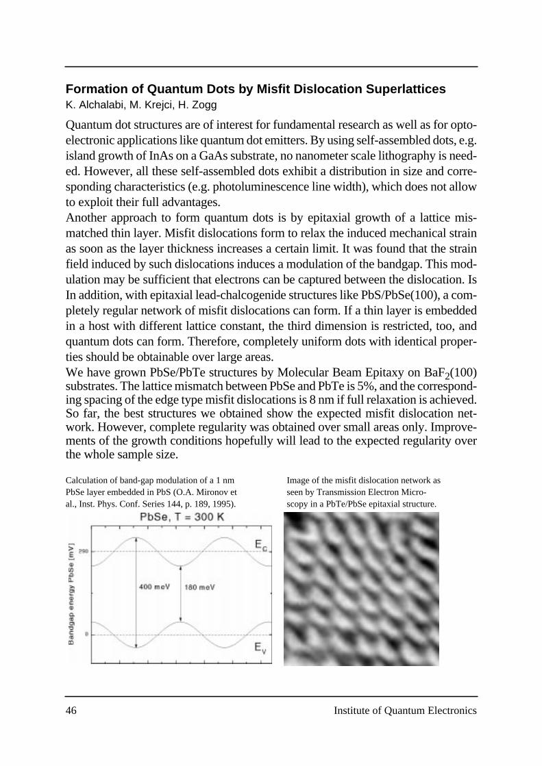
Formation of Quantum Dots by Misfit Dislocation SuperlatticesK. Alchalabi, M. Krejci, H. Zogg
Quantum dot structures are of interest for fundamental research as well as forelectronic applications like quantum dot emitters. By using self-assembled dotsisland growth of InAs on a GaAs substrate, no nanometer scale lithography ised. However, all these self-assembled dots exhibit a distribution in size and csponding characteristics (e.g. photoluminescence line width), which does notto exploit their full advantages.Another approach to form quantum dots is by epitaxial growth of a lattice mmatched thin layer. Misfit dislocations form to relax the induced mechanical sas soon as the layer thickness increases a certain limit. It was found that thefield induced by such dislocations induces a modulation of the bandgap. Thisulation may be sufficient that electrons can be captured between the dislocatiIn addition, with epitaxial lead-chalcogenide structures like PbS/PbSe(100), apletely regular network of misfit dislocations can form. If a thin layer is embedin a host with different lattice constant, the third dimension is restricted, too,quantum dots can form. Therefore, completely uniform dots with identical proties should be obtainable over large areas.We have grown PbSe/PbTe structures by Molecular Beam Epitaxy on BaF2(100)substrates. The lattice mismatch between PbSe and PbTe is 5%, and the correing spacing of the edge type misfit dislocations is 8 nm if full relaxation is achievSo far, the best structures we obtained show the expected misfit dislocationwork. However, complete regularity was obtained over small areas only. Imprments of the growth conditions hopefully will lead to the expected regularity othe whole sample size.
Calculation of band-gap modulation of a 1 nm Image of the misfit dislocation network asPbSe layer embedded in PbS (O.A. Mironov et seen by Transmission Electron Micro-al., Inst. Phys. Conf. Series 144, p. 189, 1995). scopy in a PbTe/PbSe epitaxial structure.
46 Institute of Quantum Electronics
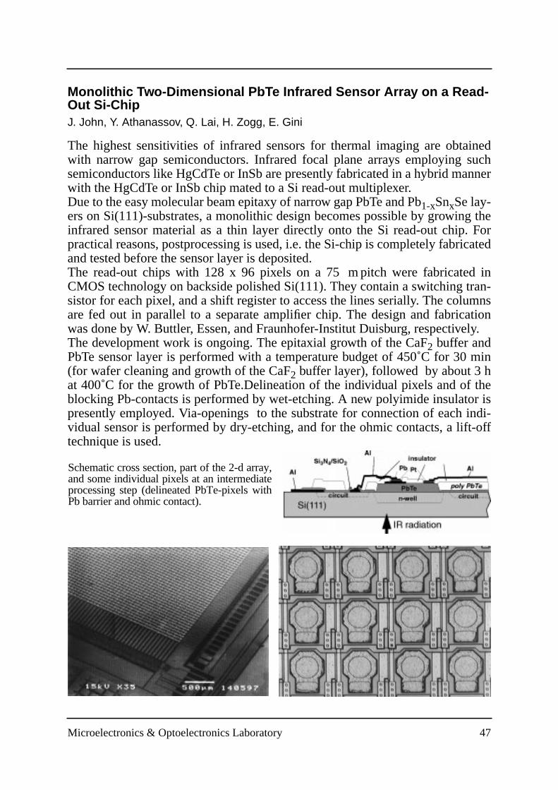
ineduchnner
g theFor
icated
inran-mnstion
ely.
min
ther isindi-
t-off
Monolithic Two-Dimensional PbTe Infrared Sensor Array on a Read-Out Si-Chip 0.28J. John, Y. Athanassov, Q. Lai, H. Zogg, E. Gini
The highest sensitivities of infrared sensors for thermal imaging are obtawith narrow gap semiconductors. Infrared focal plane arrays employing ssemiconductors like HgCdTe or InSb are presently fabricated in a hybrid mawith the HgCdTe or InSb chip mated to a Si read-out multiplexer.Due to the easy molecular beam epitaxy of narrow gap PbTe and Pb1-xSnxSe lay-ers on Si(111)-substrates, a monolithic design becomes possible by growininfrared sensor material as a thin layer directly onto the Si read-out chip.practical reasons, postprocessing is used, i.e. the Si-chip is completely fabrand tested before the sensor layer is deposited.The read-out chips with 128 x 96 pixels on a 75 m pitch were fabricatedCMOS technology on backside polished Si(111). They contain a switching tsistor for each pixel, and a shift register to access the lines serially. The coluare fed out in parallel to a separate amplifier chip. The design and fabricawas done by W. Buttler, Essen, and Fraunhofer-Institut Duisburg, respectivThe development work is ongoing. The epitaxial growth of the CaF2 buffer andPbTe sensor layer is performed with a temperature budget of 450˚C for 30(for wafer cleaning and growth of the CaF2 buffer layer), followed by about 3 hat 400˚C for the growth of PbTe.Delineation of the individual pixels and ofblocking Pb-contacts is performed by wet-etching. A new polyimide insulatopresently employed. Via-openings to the substrate for connection of eachvidual sensor is performed by dry-etching, and for the ohmic contacts, a liftechnique is used.
Schematic cross section, part of the 2-d array,and some individual pixels at an intermediateprocessing step (delineated PbTe-pixels withPb barrier and ohmic contact).
Microelectronics & Optoelectronics Laboratory 47
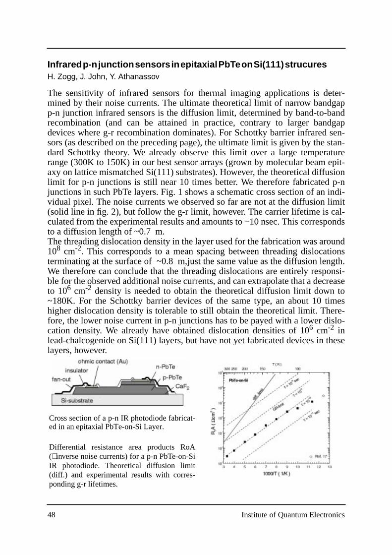
ter-gapanddgapsen-stan-tureepit-sionp-nindi-
limitl-ponds
oundtionsngth.onsi-
creaseto
imesre-islo-
these
Infraredp-njunctionsensors inepitaxialPbTeonSi(111)strucures 0.29H. Zogg, J. John, Y. Athanassov
The sensitivity of infrared sensors for thermal imaging applications is demined by their noise currents. The ultimate theoretical limit of narrow bandp-n junction infrared sensors is the diffusion limit, determined by band-to-brecombination (and can be attained in practice, contrary to larger bandevices where g-r recombination dominates). For Schottky barrier infraredsors (as described on the preceding page), the ultimate limit is given by thedard Schottky theory. We already observe this limit over a large temperarange (300K to 150K) in our best sensor arrays (grown by molecular beamaxy on lattice mismatched Si(111) substrates). However, the theoretical diffulimit for p-n junctions is still near 10 times better. We therefore fabricatedjunctions in such PbTe layers. Fig. 1 shows a schematic cross section of anvidual pixel. The noise currents we observed so far are not at the diffusion(solid line in fig. 2), but follow the g-r limit, however. The carrier lifetime is caculated from the experimental results and amounts to ~10 nsec. This corresto a diffusion length of ~0.7 m.The threading dislocation density in the layer used for the fabrication was ar108 cm-2. This corresponds to a mean spacing between threading dislocaterminating at the surface of ~0.8 m,just the same value as the diffusion leWe therefore can conclude that the threading dislocations are entirely respble for the observed additional noise currents, and can extrapolate that a deto 106 cm-2 density is needed to obtain the theoretical diffusion limit down~180K. For the Schottky barrier devices of the same type, an about 10 thigher dislocation density is tolerable to still obtain the theoretical limit. Thefore, the lower noise current in p-n junctions has to be payed with a lower dcation density. We already have obtained dislocation densities of 106 cm-2 inlead-chalcogenide on Si(111) layers, but have not yet fabricated devices inlayers, however.
Cross section of a p-n IR photodiode fabricat-ed in an epitaxial PbTe-on-Si Layer.
Differential resistance area products RoA(∼inverse noise currents) for a p-n PbTe-on-SiIR photodiode. Theoretical diffusion limit(diff.) and experimental results with corres-ponding g-r lifetimes.
48 Institute of Quantum Electronics
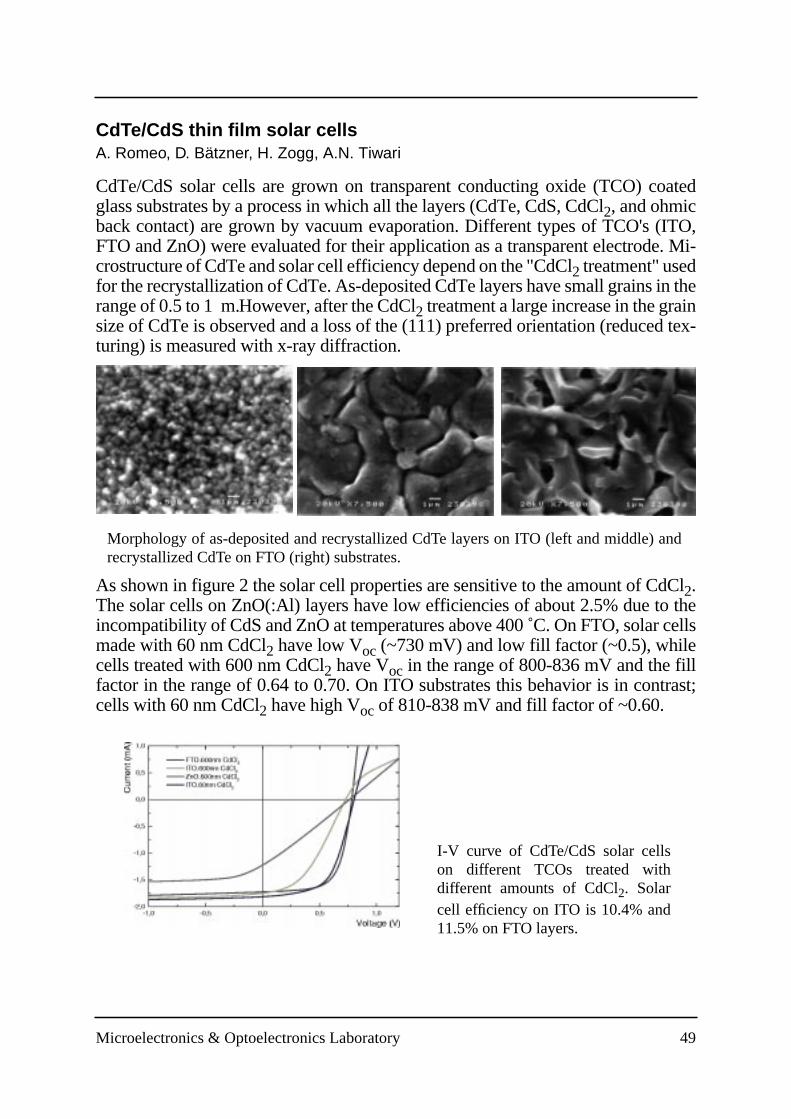
ated
ITO,. Mi-
n theind tex-
Clthe
cells
ltrast;
nd
CdTe/CdS thin film solar cellsA. Romeo, D. Bätzner, H. Zogg, A.N. Tiwari
CdTe/CdS solar cells are grown on transparent conducting oxide (TCO) coglass substrates by a process in which all the layers (CdTe, CdS, CdCl2, and ohmicback contact) are grown by vacuum evaporation. Different types of TCO's (FTO and ZnO) were evaluated for their application as a transparent electrodecrostructure of CdTe and solar cell efficiency depend on the "CdCl2 treatment" usedfor the recrystallization of CdTe. As-deposited CdTe layers have small grains irange of 0.5 to 1 m.However, after the CdCl2 treatment a large increase in the grasize of CdTe is observed and a loss of the (111) preferred orientation (reduceturing) is measured with x-ray diffraction.
As shown in figure 2 the solar cell properties are sensitive to the amount of Cd2.The solar cells on ZnO(:Al) layers have low efficiencies of about 2.5% due toincompatibility of CdS and ZnO at temperatures above 400 ˚C. On FTO, solarmade with 60 nm CdCl2 have low Voc (~730 mV) and low fill factor (~0.5), whilecells treated with 600 nm CdCl2 have Voc in the range of 800-836 mV and the filfactor in the range of 0.64 to 0.70. On ITO substrates this behavior is in concells with 60 nm CdCl2 have high Voc of 810-838 mV and fill factor of ~0.60.
Morphology of as-deposited and recrystallized CdTe layers on ITO (left and middle) arecrystallized CdTe on FTO (right) substrates.
I-V curve of CdTe/CdS solar cellson different TCOs treated withdifferent amounts of CdCl2. Solarcell efficiency on ITO is 10.4% and11.5% on FTO layers.
Microelectronics & Optoelectronics Laboratory 49

oly-
mis-truc-the
d ab-
copyse of
i-
)Se
Growth and characterization of heteroepitaxial CuIn ySey layers andinterfacesM. Krejci, F. -J. Haug, H. Zogg, A.N. Tiwari
Chalcopyrite (CuInSe2) and defect-chalcopyrite (different In-rich CuInxSey com-positions) compounds are important materials for stable and high efficiency pcrystalline thin film solar cells. Heteroepitaxial layers of CuInxSey were grown onSi and GaAs substrates by molecular beam epitaxy. Despite of large latticematch and different thermal expansion coefficients, epitaxial layers of “good stural quality” have been obtained. X-ray diffraction (XRD) measurements andanalyses of the lattice vibrational properties by Raman scattering and infraresorption show (fig. 1) that the CuIn2.5Se4 ( β-phase), CuIn3Se5, and CuInSe2 aresingle phase compounds while CuIn1.6Se2.9 is a mixture of CuInSe2 ( β-phase)andCuIn2.5Se4 ( α-phase) compounds.
Transmission electron microscopy (TEM), Rutherford backscattering spectrosand XRD were used to investigate the substrate-layer interfaces. In the caCuInxSey/Si an interfacial CuSixSey layer is formed during the growth of the eptaxial layer. However, for CuInxSey/GaAs, a strong diffusion of Ga into the CuInx-Sey is observed. XRD measurements show the formation of the Cu(In,Ga2quaternary compound at the interface.
IR absorption spectra and XRD of epitaxial CuInxSey/Si(111) layers.
XRD of CuInxSey/GaAs shows theformation of an interfacialCu(In,Ga)Se2 compound.
50 Institute of Quantum Electronics
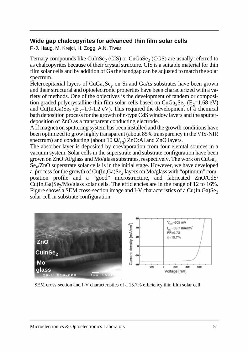
r thinsolar
wna va-
posi-
calutter-
have-NIR
s in ae beenGaoped
dS/6%.a)Se
Wide gap chalcopyrites for advanced thin film solar cellsF.-J. Haug, M. Krejci, H. Zogg, A.N. Tiwari
Ternary compounds like CuInSe2 (CIS) or CuGaSe2 (CGS) are usually referred toas chalcopyrites because of their crystal structure. CIS is a suitable material fofilm solar cells and by addition of Ga the bandgap can be adjusted to match thespectrum.Heteroepitaxial layers of CuGaxSey on Si and GaAs substrates have been groand their structural and optoelectronic properties have been characterized withriety of methods. One of the objectives is the development of tandem or comtion graded polycrystalline thin film solar cells based on CuGaxSey (Eg=1.68 eV)and Cu(In,Ga)Se2 (Eg=1.0-1.2 eV). This required the development of a chemibath deposition process for the growth of n-type CdS window layers and the spdeposition of ZnO as a transparent conducting electrode.A rf magnetron sputtering system has been installed and the growth conditionsbeen optimized to grow highly transparent (about 85% transparency in the VISspectrum) and conducting (about 10Ω/sq) ZnO:Al and ZnO layers.The absorber layer is deposited by coevaporation from four elemtal sourcevacuum system. Solar cells in the superstrate and substrate configuration havgrown on ZnO:Al/glass and Mo/glass substrates, respectively. The work on Cux-Sey/ZnO superstrate solar cells is in the initial stage. However, we have devela process for the growth of Cu(In,Ga)Se2 layers on Mo/glass with “optimum” com-position profile and a “good” microstructure, and fabricated ZnO/CCu(In,Ga)Se2/Mo/glass solar cells. The efficiencies are in the range of 12 to 1Figure shows a SEM cross-section image and I-V characteristics of a Cu(In,G2solar cell in substrate configuration.
SEM cross-section and I-V characteristics of a 15.7% efficiency thin film solar cell.
ZnO
CuInSe2
Moglass
Microelectronics & Optoelectronics Laboratory 51

52 Institute of Quantum Electronics

l
l
s"
ents
PUBLICATIONS 1998 0.210.22
Microelectronics and Optoelectronics Laboratory 0.230.24
Books, Book Chapters and Reviews 0.25
R. Bauknecht"InP Double Heterojunction Bipolar Transistors for Driver Circuits in Fiber OpticaCommunication Systems"Hartung-Gorre Verlag Konstanz, Series in Microelectronics,72, 203 pages,ISBN 3-89649-264-0, 1998
J. Eckner"Semiconductor Optical Amplifiers: Optimization of Polarization and MonolithicaIntegration in Ridge Waveguide Bulk InGaAsP/InP"Hartung-Gorre Verlag Konstanz, Series in Quantum Electronics, 8, 201 pages,ISBN 3-89649-375-2, 1998
G. Guekos (Ed.)"Photonic Devices for Telecommunications"Springer Verlag, Hardcover, 404 pages, ISBN 3-540-64318-4, 1998
R. Hess"Ultrafast All-Optical Time Demultiplexer for Optical Telecommunication SystemHartung-Gorre Verlag Konstanz, Series in Quantum Electronics,6, 120 pages,ISBN 3-89649-297-7, 1998
R. Krähenbühl"Electro-Optic Space Switches in InGaAsP/InP for Optical Communication"Hartung-Gorre Verlag Konstanz, Series in Quantum Electronics,4, 202 pages,ISBN 3-89649-267-5, 1998
Q. Lai"Silica on Silicon Waveguides with Square diffused Structure and their Componfor Optical Fiber Communication"Hartung-Gorre Verlag Konstanz, Series in Quantum Electronics,7, 135 pages,ISBN 3-89649-314-0, 1998
P. Nizzola"Clock and Data Recovery Circuit for Protocol- and Bitrate-Independent DataNetworks"Hartung-Gorre Verlag Konstanz, Series in Microelectronics,76, 117 pages,ISBN 3-89649-353-1, 1998
Microelectronics & Optoelectronics Laboratory 53
ed
, M.
ut
oise
pan,
s
y
"
Journal Publications 0.26
Y. Acremann, T. Heinzel, K. Ensslin, M. Holland, E. Gini and H. Melchior"Individual Scatterers as Microscopic Origin of Equilibration between Spin-PolarizEdge Channels in the Quantum Hall Regime"Physical Review B,59, pp. 2116 - 2119, Jan. 1999
D. Chiaroni, B. Lavigne, L. Hamon, A. Jourdan, F. Dorgeuille, C. Janz, E. GrardRenaud, R. Bauknecht, C. Graf, H.P. Schneibel and H. Melchior"Experimental Validation of an All-Optical Network Based on 160 Gbit/s ThroughpPacket Switching Nodes"Proc. ECOC’98, pp. 573 - 574, Sept. 1998
G. Contestabile, F. Martelli, A. Mecozzi, L. Graziani, A. D'Ottavi, P. Spano,G. Guekos, R. Dall'Ara and J. Eckner"Efficiency Flattening and Equalization of Frequency Up- and Down-ConversionUsing Four-Wave Mixing in Semiconductor Optical Amplifiers"IEEE Photonics Techn. Letters,10, pp. 1398 - 1400, Oct. 1998
G. Contestabile, M. Greco, F. Martelli, A. Mecozzi, A. D'Ottavi, P. Spano,R. Dall'Ara and G. Guekos"Frequency Up- and Down-Conversion with Constant Efficiency and Signal-to-NRatio using Four-Wave Mixing in Semiconductor Optical Amplifiers"Conf. Digest, 1998 IEEE International Semiconductor Laser Conference, Nara, Japp. 31 - 32, Oct. 1998
A. Corchia, C. Antonini, A. D'Ottavi, A. Mecozzi, F. Martelli, P. Spano, G. Guekoand R. Dall'Ara"Dispersion Compensation using Mid-Span Spectral Inversion without FrequencShift "Proc. ECOC’98, Madrid, pp. 511 - 512, Sept. 1998
B. Dhoedt, R. Baets, P. van Daele, P. Heremans, J. van Campenhout, J. Hall,R. Michalzik, H. Thienpont, R. Vounckx, A. Neyer, D.C. O’Brien, J. van Koetsemand A. Schmid"Optically Interconnected Integrated Circuits to solve the CMOS InterconnectBottleneck"Electronic Components & Technology Conference, Seattle, Washington, USA,pp. 992 - 998, May 1998
F. Dorgeuille, B. Lavigne, J.Y. Emery, M. Di Maggio, J. Le Bris, D. Chiaroni,M. Renaud, R. Bauknecht, H.P. Schneibel, C. Graf and H. Melchior"Fast Optical Amplifier Gate Array for WDM Routing and Switching ApplicationsOFC’98 Technical Digest, Vol. 2, pp. 42 - 44, Feb. 1998
54 Institute of Quantum Electronics
l"
ors"
nry,
s in
hior
pan,
A. D'Ottavi, P. Spano, G. Hunziker, R. Paiella, R. Dall'Ara, G. Guekosand K. J. Vahala"Wavelength Conversion at 10 Gb/s by Four-Wave Mixing over a 30-nm IntervaIEEE Photon. Technol. Lett.,10, pp. 952 - 954, July 1998
R. Fluck, R. Häring, R. Paschotta, E. Gini, U. Keller and H. Melchior"Eyesafe Pulsed Microchip Laser using Semiconductor Saturable Absorber MirrApplied Physics Letters,72, pp. 3272 - 3275, June 1998
P. Gambini, M. Renaud, Ch. Guillemot, F. Callegati, I. Andonovic, B. Bostica,D. Chiaroni, G. Corazza, S.L. Danielson, P. Gravey, P. Bukhave Hansen, M. HeCh. Janz, A. Kloch, C. Raffaelli, M. Schilling, A. Talneau, L. Zucchelli andR. Krähenbühl,"Transparent Optical Packet Switching: Network Architecture and Demonstratorthe KEOPS Project"IEEE Journal on Selected Areas in Communications,16, pp. 1245 - 1259, Sept. 1998
E. Gini, W. Hunziker and H. Melchior"Polarization Independent InP WDM Multiplexer/Demultiplexer Module"Journal of Lightwave Technology,16, pp. 625 - 630, April 1998
F. Girardin, G. Guekos and A. Houbavlis"Gain Recovery of Bulk Semiconductor Optical Amplifiers"IEEE Photon. Technol. Lett.,10, pp. 784 - 786, June 1998
F. Girardin, G. Guekos and A. Mecozzi"Nearly Degenerate Four-Wave Mixing in Semiconductor Optical Amplifiers"Proc. CLEO/Europe ‘98, Glasgow, UK, paper CTh H18, Sept. 1998
F. Girardin, J. Leuthold, P. A. Besse, E. Gamper, W. Vogt, G. Guekos and H. Melc"Monolithically Integrated MZI-SOA Configuration for Polarization IndependentOptical Phase Conjugation with Pump Filtering"Conf. Digest, 1998 IEEE International Semiconductor Laser Conference, Nara, Japp. 37 - 38, Oct. 1998
K. Hamamoto, E. Gini, C. Holtmann, and H. Melchior"Single Transverse Mode Active Multimode Interferometer InGaAsP/InP LaserDiode"IEE Electronics Letters,34, pp. 462 - 464, March 1998
K. Hamamoto, E. Gini, C. Holtmann and H. Melchior"Single Transverse Mode Active MMI InGaAsP/InP Laser Diode"Proc. 1998 Integrated Photonics Research Conference, Victoria B.C. Canada,pp. 186 - 188, April 1998
Microelectronics & Optoelectronics Laboratory 55
or
and
e,
t,
rone,lchior-
0,
nd
alactor
R. Hess, M. Caraccia-Gross, W. Vogt, E. Gamper, P.A. Besse, M. Dülk, E. Gini,B. Mikkelsen, M. Vaa, K.S. Jepsen, K.E. Stubkjaer, S. Bouchoule and H. Melchi"All-Optical Demultiplexing of 80 to 10 Gb/s Signals with Monolithic IntegratedHigh-Performance Mach-Zehnder Interferometer"IEEE Photonics Technology Letters,10, pp. 165 - 167, Jan. 1998
R. Hess, M. Duelk, W. Vogt, E. Gamper, E. Gini, P.A. Besse, K.S. Jepsen,B. Mikkelsen, M. Vaa, H.N. Poulsen, A.T. Clausen, K.E. Stubkjaer, S. BouchouleH. Melchior"Simultaneous all-Optical Add and Drop Multiplexing of 40 Gb/s OTDM Signalsusing Monolithically Integrated Mach-Zehnder Interferometer"Technical Digest, OFC’98, pp. 310 - 311, Feb. 1998.
R. Hess, M. Duelk, W. Vogt, E. Gamper, E. Gini, P.A. Besse, K.S. Jepsen,B. Mikkelsen, M. Vaa, H.N. Poulsen, A.T. Clausen, K.E. Stubkjaer, S. BouchoulF. Devaux and H. Melchior"Simultaneous All-Optical Add and Drop Multiplexing of 40 Gbit/s OTDM Signalsusing Monolithically Integrated Mach-Zehnder Interferometer"IEE Electronics Letters,34, pp. 579 - 580, March 1998
R. Hess, M.W. Chbat, E. Grard, L. Berthelon, A. Jourdan, P.A. Perrier, A. LeclerB. Landousies, A. Ramdane, N. Parnis, E.V. Jones, E. Limal, H.N. Poulsen,R.J.S. Pedersen, N. Flaarønning, D. Vercauteren, M. Puleo, E. Ciaramella, G. MaW. van Parys, P.M. Demeester, P.J. Gødsvang, T. Olsen, D.R. Hjelme and H. Me"Toward Wide-Scale All-Optical Transparent Networking: The ACTS Optical PanEuropean Network (OPEN) Project"IEEE Journal on Selected Areas in Communications,16, pp. 1226 - 1244, Sept. 1998
C. Holtmann"Integration and Applications of III-V Semiconductor Optical Amplifiers"Proc. European Conference on Optical Communication, ECOC’98, pp. 499 - 50Sept.1998
D. Huber, M. Bitter, S. Romier, I. Schnyder, T. Morf, C. Bergamaschi, H. Jäckel aR. Bauknecht"23 GHz Monolithically Integrated InP/InGaAs PIN/HBT-Receiver with 12 THzΩGain-bandwidth Product"Proc. IPRM’98, Tsukuba, Japan, pp. 447 - 450, May 1998
G. Hunziker, R. Paiella, A. D'Ottavi, P. Spano, R. Dall'Ara, G. Guekos and K. Vah"30 nm Wavelength Conversion at 10 Gb/s by Four-Wave Mixing in a SemiconduOptical Amplifier"OFC'98 Technical Digest, pp. 108 - 109, Feb.1998
56 Institute of Quantum Electronics

ent"
th
d
rol-
in a
i-
W. Hunziker"Ways to Cost Effective Packaging: Waveguide Tapers and Passive Self-AlignmProc. IEEE/LEOS,1, pp. 36 - 37, Dec.1998
Q. Lai, M. Lanker, W. Hunziker and H. Melchior"Tunable Wavelength-Selection Switch and Multiplexer/Demultiplexer Based onAsymmetric Silica-on-Silicon Mach-Zehnder Interferometer"Electronic Letters,34, pp. 266 - 267, Feb. 1998
Q. Lai, W. Hunziker and H. Melchior"Low-Power Compact 2 x 2 Thermooptic Silica-on-Silicon Waveguide Switch wiFast Response"IEEE Photonics Technology,10, pp. 681 - 683, May 1998
J. Leuthold, P.A. Besse, J. Eckner, E. Gamper, M. Dülk and H. Melchior"All-Optical Space Switches with Gain and Principally Ideal Extinction Ratios"IEEE Journal of Quantum Electronics,34, pp. 622 - 633, April 1998
J. Leuthold, J. Eckner, E. Gamper, P.A. Besse and H. Melchior"Multimode Interference Couplers for the Conversion and Combining of Zero- anFirst-Order Modes"Journal of Lightwave Technology,16, pp. 1228 - 1239, July 1998
J. Leuthold, P.A. Besse, E. Gamper, M. Dülk, S. Fischer and H. Melchior"Cascadable Dual-Order Mode All-Optical Switch with Integrated Data- and ContSignal Separators"IEE Electronics Letters,34, pp. 1598 - 1600, Aug. 1998
J. Leuthold, P.A. Besse, E. Gamper, M. Dülk, W. Vogt and H. Melchior"Cascadable MZI-All-Optical Switch with Separate Ports for Data- and Control-Signals"Proc. ECOC’98, Madrid, Spain, pp. 463 - 464, Sept. 1998
J. Leuthold, F. Girardin, P.A. Besse, E. Gamper, G. Guekos and H. Melchior"Polarization Independent Optical Phase Conjugation with Pump-Signal FilteringMonolithically Integrated Mach-Zehnder Interferometer Semiconductor OpticalAmplifier Configuration"IEEE Photonics Technology Letters,10, pp.1569 - 1571, Nov. 1998
A. Mecozzi, G. Contestabile, F. Martelli, L. Graziani, A. D'Ottavi, P. Spano,G. Guekos, R. Dall'Ara and J. Eckner"Efficiency Equalization of Up- and Down-Conversion Four-Wave Mixing in a Semconductor Optical Amplifier using two Pumps with Orthogonal Polarization"OFC'98 Technical Digest, pp. 107 - 108, Feb.1998
Microelectronics & Optoelectronics Laboratory 57
r"
s"0,
rnal
za-
and,
e
y
in a
A. Mecozzi, G. Contestabile, F. Martelli, L. Graziani, A. D'Ottavi, P. Spano,R. Dall'Ara, J. Eckner, F. Girardin and G. Guekos"Optical Spectral Inversion without Frequency Shift by Four-Wave Mixing UsingTwo Pumps with Orthogonal Polarization"IEEE Photonics Techn. Letters,10, pp. 355 - 357, March 1998
A. Mecozzi, G. Contestabile, L. Graziani, F. Martelli, A. D’Ottavi, P. Spano,R. Dall’Ara and J. Eckner"Polarization-Insensitive Four-Wave Mixing in a Semiconductor Optical AmplifieApplied Physics Letters,72, pp. 2651 - 2653, May 1998
C. Nadler, M. Lanker, E. Wildermuth, W. Hunziker and H. Melchior"Polarization Insensitive Wavelength Multiplexers Using Stress Release GrooveProc. European Conference on Optical Communication, ECOC’98, pp. 129 - 13Sept. 1998
S. Pajarola, G. Guekos and H. Kawaguchi"Dual-Polarization Optical Pulse Generation using a Mode-Locked two-arm ExteCavity Diode Laser"Optics Communications,154, pp. 39 - 42, Aug. 1998
S. Pajarola, G. Guekos, and H. Kawaguchi"Data Transission on Optically Generated Millimeter-Waves using a Dual-Polarition Emission External Cavity Diode Laser"Proc. 1998 International Zurich Seminar on Broadband Communications, Switzerlpp. 59 - 62, Feb.1998 (IEEE Catalog No. 98TH8277)
S. Pajarola, G. Guekos and H. Kawaguchi"Antenna Remote Fiber Feeding Using a Dual-polarization External Cavity DiodLaser"Proc. ICT'98 Intern. Conf. on Telecommunications, Porto Carras, Greece,pp. 344 - 347, June 1998
S. Pajarola, G. Guekos and H. Kawaguchi"Optical Millimeter-Wave Transmission Using a Dual-polarization External CavitDiode Laser"IEEE Photon. Technol. Lett., 10, pp. 1021 - 1023, July 1998
T. Pliska, D. Fluck, P. Günter, E. Gini, L. Beckers, A. Eckau, C. Buchal andH. Melchior"Efficient Birefringence Phase-Matched Blue Light Second-Harmonic GenerationKNbO3 Ridge Waveguide"Proc. Nonlinear Guided Waves & Their Applications ‘98, Optical Soc., America,April 1998
58 Institute of Quantum Electronics

bO
lle,
T. Pliska, D. Fluck, G. Günter, E. Gini, L. Beckers, C. Buchal and H. Melchior"Birefringence Phase-Matched Blue Light Second Harmonic Generation in a KN3Ridge Waveguide"Applied Physics Letters,72, pp. 2364 - 2366, May 1998
H.N. Poulsen, K.S. Jepsen, A.T. Claussen, A. Buxens, K.E. Stubkjaer, R. Hess,M. Dülk and H. Melchior"Fast Optical Signal Processing in High Bit Rate OTDM Systems"Proc. IEEE/LEOS,1, pp. 67 - 68, Dec. 1998
I. Tomkos, I. Zacharopoulos, E. Roditi, D. Syvridis, F. Girardin, L. Occhi andA. Uskov"Highly Performing Wavelength Converter Based on Dual Pump Wave Mixing inSemiconductor Optical Amplifier"Proc. LEOS ‘98, Orlando, USA, pp. 71 - 72, Dec. 1998
E. Wildermuth, Ch. Nadler, M. Lanker, W. Hunziker and H. Melchior"Penalty-free Polarisation Compensation of SiO2/Si Arrayed Waveguide GratingWavelength Multiplexers using Stress Release Grooves"IEE Electronics Letters,34, pp. 1661 - 1663, Aug. 1998
L. Zucchelli, D. Di Bella, G. Fornuto, P. Gambini, D. Re, F. Delorme,R. Kraehenbuehl and H. Melchior"An Experimental Optical Packet Synchroniser with 100 ns Range and 200 psResolution"Proc. ECOC’98, pp. 587 - 588, Sept. 1998
ORAL PRESENTATIONS 1998 0.27
L. Alimkulova"The Electrical, Structural and Optical Properties of AlGaInAs/InGaAs QuantumWell Structures"Poster 40th Electronic Materials Conference, University of Virginia, CharlottesviVirginia, USA, June 1998
L. Alimkulova"The Low Loss Waveguides based on InAlAs/InP Materials"Meeting Priority Program Optique, Geneva, June 18, 1998
L. Alimkulova"Linear and Nonlinear Optical Properties of Low-Dimensional SemiconductorNanostructures"Meeting Priority Program Optique, Berne, Switzerland, Nov. 5, 1998
Microelectronics & Optoelectronics Laboratory 59
nds,
M.
ut
UK,
- 8,
30 -
’98,
hi
ing
y,
M. Caraccia-Gross"Optically Controlled Mach-Zehnder Interferometers: Modeling and Experiment"Symposium on Ultrafast Photonic Processing and Networks, The Rank Prize FuGrasmere, Great-Britain, April 20 - 23, 1998
D. Chiaroni, B. Lavigne, L. Hamon, A. Jourdan, F. Dorgeuille, C. Janz, E. Grard,Renaud, R. Bauknecht, C. Graf, H.P. Schneibel and H. Melchior"Experimental Validation of an All-Optical Network Based on 160 Gbit/s ThroughpPacket Switching Nodes"ECOC’98, Madrid, Spain, Sept. 20 - 24, 1998
F. Girardin, G. Guekos and A. Mecozzi"Nearly Degenerate Four-Wave Mixing in Semiconductor Optical Amplifiers"Conference on Lasers and Electro-Optics Europe, CLEO/Europe ‘98, Glasgow, Sept. 14 - 18, 1998
F. Girardin, J. Leuthold, P. A. Besse, E. Gamper, W. Vogt, G. Guekos andH. Melchior"Monolithically Integrated MZI-SOA Configuration for Polarization IndependentOptical Phase Conjugation with Pump Filtering"1998 IEEE International Semiconductor Laser Conference, Nara, Japan, Oct. 4 1998
K. Hamamoto, E. Gini, C. Holtmann and H. Melchior"Single Transverse Mode Active MMI InGaAsP/InP Laser Diode"1998 Integrated Photonics Research Conference, Victoria B.C. Canada, March April 1, 1998
C. Holtmann"Integration and Applications of III-V Semiconductor Optical Amplifiers"Invited presentation at European Conference on Optical Communication ECOCSept. 20 - 24, 1998
D. Huber, S. Romier, I. Schnyder, R. Bauknecht, M. Bitter, T. Morf, C. Bergamascand H. Jäckel"23 GHz Monolithically Integrated InP/InGaAs PIN/HBT-Receiver with 12 THzΩGain-Bandwidth Product"International Conference on Indium Phosphide and Related Materials IPRM,Tsukuba, Japan, May 11 - 15, 1998
W. Hunziker"Packaging of Optoelectronic Components: Fiber Array Connections and MountPlatforms"Seminar at Institute of Microsystems of the Swiss Federal Institute of TechnologLausanne, Switzerland, Jan.19, 1998
60 Institute of Quantum Electronics
ent"
on
S.
ig-
1998
98
s"
W. Hunziker"Ways to Cost Effective Packaging: Waveguide Tapers and Passive Self-AlignmIEEE/LEOS 11th Annual Meeting, Orlando, Florida, USA, Dec.1 - 2, 1998
M. Lanker, E. Wildermuth, Ch. Nadler,W. Hunziker and H. Melchior"Technology for Polarization Insensitive Arrayed Waveguide Multiplexers BasedSiO2 on Si"Workshop on Fibre Optic Passive Components, WFOPC’98, Pavia,Sept. 18, 1998
K.S. Jepsen, B. Mikkelsen, M. Vaa, H.N. Poulsen, A.T. Clausen, K.E. Stubkjaer, Bouchoule, R. Hess, M. Duelk, W. Vogt, E. Gamper, E. Gini, P.A. Besse andH. Melchior"Simultaneous all-Optical Add and Drop Multiplexing of 40 Gb/s OTDM Signalsusing Monolithically Integrated Mach-Zehnder Interferometer"OFC’98, Feb. 1998.
J. Leuthold, P.A. Besse, E. Gamper, M. Dülk, W. Vogt and H. Melchior"Cascadable MZI-All-Optical Switch with Separate Ports for Data- and Control-Snals"European Conference on Optical Communication, Madrid, Spain, Sept. 20 - 24
H. Melchior"Indium Phosphide Waveguide Devices and their Fiber Pigtailing"Invited Plenary Presentation, 1998 Integrated Photonics Research Conference,Victoria B.C. Canada, March 30 - April 1, 1998
H. Melchior"Indium Phosphide Optical Waveguide Switches and Optical Amplifiers"Seminar, NEC Corporation Research Laboratories, Tsukuba, Japan, May 18, 19
H. Melchior"Optoelectronic Waveguide Component Modules"Seminar, Hitachi Central Research Laboratories, Tokyo, May 10, 1998
H. Melchior"Optical Waveguide Switches, Amplifiers and Demultiplexers for Fiber-OpticalNetworks"Seminar, NTT-Research Laboratories, Atsugi, Japan, May 21, 1998
C. Nadler, M. Lanker, E. Wildermuth, W. Hunziker and H. Melchior"Polarization Insensitive Wavelength Multiplexers Using Stress Release GrooveEuropean Conference on Optical Communication, ECOC’98, Madrid,Sept. 20 - 24, 1998
Microelectronics & Optoelectronics Laboratory 61
e
ne,
tion
d,
in a
,
S. Pajarola,G. Guekos and H. Kawaguchi"Antenna Remote Fiber Feeding Using a Dual-polarization External Cavity DiodLaser"ICT '98, Intern. Conf. on Telecommunications, Porto Carras, Greece, 21 - 25 Ju1998
S. Pajarola, G. Guekos and H. Kawaguchi"Data transmission on optically generated millimeter-waves using a dual-polarizaemission external cavity diode laser"1998 Intern. Zurich Seminar on Broadband Communications, Zurich, SwitzerlanFeb. 17 - 19, 1998
S. Pajarola, L. Occhi, G. Guekos and H. Kawaguchi"Optical millimeter-wave generation for remote antenna feeding using a dual-polarization external cavity diode laser"6th MCM COST 259, Duisburg, Germany, Sept. 23 - 25, 1998
T. Pliska, D. Fluck, G. Günter, E. Gini, L. Beckers, C. Buchal and H. Melchior"Efficient Birefringence Phase-Matched Blue Light Second Harmonic GenerationKNbO3 Ridge Waveguide"Nonlinear Waveguide and their Applications Conference, Victoria, B.C. CanadaApril 1 - 3, 1998
H.N. Poulsen, K.S. Jepsen, A.T. Claussen, A. Buxens, K.E. Stubkjaer, R. Hess,M. Dülk and H. Melchior"Fast Optical Signal Processing in High Bit Rate OTDM Systems"IEEE/LEOS 11th Annual Meeting, Orlando, Florida, USA, Dec. 1 - 4, 1998
L. Zucchelli, D. Di Bella, G. Fornuto, P. Gambini, D. Re, F. Delorme,R. Kraehenbuehl and H. Melchior"An Experimental Optical Packet Synchroniser with 100 ns Range and 200 psResolution"ECOC’98, Madrid, Spain, Sept. 20 - 24, 1998
62 Institute of Quantum Electronics
t
m
1)"
Thin Film Physics Group 0.280.29
Journal Publications 0.30
M.J. Furlong, M. Froment, M.C. Berhard, R. Cortès, A.N. Tiwari, M. Krejci, D. Lincoand H. Zogg"Aqueous Solution Epitaxy of CdS Layers on CuInSe2"Journal Crystal Growth,193, pp. 114 - 122, 1998
M. Krejci, A.N. Tiwari, M. Döbeli, V. Zelezny, J. Oswald, V. Vorlicek and H. Zogg"Epitaxial CuInxSey Layers of Improved Crystal Quality and Determination of theCrystal Orientation with Raman Spectroscopy"Inst. Phys. Conference,152, pp. 377 - 380, 1998
Z. Shi, H. Zogg, U. Keller"Thick Crack-Free CaF2 Epitaxial Layer on GaAs (100) Substrate by Molecular BeaEpitaxy" Journal Electronic Mat.,27, pp. 55 - 58, 1998
A.N. Tiwari, F.-J. Haug and H. Zogg"Dünnschichtsolarzellen aus Verbindungshalbleitern"VSE Bulletin,89, pp. 45 - 49, 1998
H. Zogg and J. John"Lead Chalcogenide on Silicon Infrared Sensor Arrays"Opto-Electronics Review,6, pp. 37 - 46, 1998
Conference Presentations 0.31
K. Alchalabi, J. John and H. Zogg"Versetzungsgleiten und Reaktionen in Epitaktischem PbTe und PbSe auf Si(11SPG-Meeting, Berne, Switzerland, Feb. 26 - 27, 1998
K. Alchalabi, M. Krejci and H. Zogg"Bleisalzversetzungsübergitter auf BaF2(100)"MBE-Workshop, Hamburg, Germany, Sept. 21 - 23, 1998
F.-J. Haug, M. Krejci, A.N. Tiwari and H. Zogg"Growth and Application of Cu(In,Ga)xSey Layers"SPG Meeting, Berne, Feb. 26 - 27, 1998
Microelectronics & Optoelectronics Laboratory 63

k
998
lar
y"
F.-J. Haug, M. Krejci, A.N. Tiwari, H. Zogg, M. Döbeli, V. Zelezny and V. Vorlice"Growth and Structural Characterisation of CuGaxSey Layers"Poster, 2nd World Conference on PV Solar Energy Conversion, Vienna, Italy,July 6 - 10, 1998
J. John, H. Zogg, K. Alchalabi and Y. Athanassov"Photovoltaic Lead-Salt on Silicon IR-Sensors for the MWIR: Experimental vsTheoretical Performance"MRS (Material Research Society) Fall Meeting, Boston, USA, Nov. 30 - Dec. 4, 1
M. Krejci, F.-J. Haug, A.N. Tiwari and H. Zogg"Interfaces Between Epitaxial CuInxSey and Si and GaAs Substrates"SPG Meeting, Berne, Feb. 26 - 27, 1998
M. Krejci, A.N. Tiwari, F.-J. Haug and H. Zogg"Investigation of the Interfaces Between Substrate and Epitaxial CuInxSey Layers"Poster, 2nd World Conference on PV Solar Energy Conversion, Vienna, Italy,July 6 - 10, 1998
V. Nadenau, H.-W. Schock, M. Krejci, F.-J. Haug, A.N. Tiwari and H. Zogg"Microstucture of Cu-rich CuGaSe2 thin films"Poster, Polyse, Stuttgart, Germany, Sept. 13 - 18, 1998
A. Romeo, A.N. Tiwari, H. Zogg, M. Wagner and J.R. Günter"Influence of Transparent Conducting Ocides on the Properties of CdTe/CdS SoCells"Poster, 2nd World Conference on PV Solar Energy Conversion, Vienna, Italy,July 6 - 10, 1998
S. Schön, H. Zogg and U. Keller"Growth of Novel Broadband High Reflection Mirrors by Molecular Beam EpitaxXth International Conference on Molecular Beam Epitaxy, Cannes, France,Aug. 31 - Sept. 5, 1998
A.N. Tiwari, M. Krejci, F.-J. Haug, A. Romeo and H. Zogg"Dünnschichtsolarzellen aus Verbindungshalbleitern"National Photovoltaic Meeting, Berne, May 5, 1998
A.N. Tiwari, M. Krejci, F.-J. Haug, H. Zogg, M. Döbeli, V. Zelezny, V. Vorlicek andG. Lippold"Structural Properties and Identification of In-rich CuInxSey Phases"Poster, 2nd World Conference on PV Solar Energy Conversion, Vienna, Italy,July 6 - 10, 1998
64 Institute of Quantum Electronics
k
ce,
s"l
rs
998
A.N. Tiwari, M. Krejci, F.-J. Haug, H. Zogg, M. Döbeli, V. Zelezny and V. Vorlice"Heteroepitaxy of CuInxSey: Material for High Efficiency and Stable Solar Cells"Poster, Xth International Conference on Molecular Beam Epitaxy, Cannes, FranAug. 31 - Sept. 5, 1998
A.N. Tiwari, M. Krejci, F.-J. Haug, A. Romeo and H. Zogg"Dnnschichtsolarzellen aus Verbindungshalbleitern"SPG Energy Symposium, Airolo, Switzerland, Sept. 25, 1998
H. Zogg"Epitaxial Lead-Chalcogenide on Silicon Layers for Thermal Imaging ApplicationInvited Paper, Fourth International Conference on Material Science and MateriaProperties for Infrared Optoelectronics, Kiev, Ukraine, Sept. 28 - Oct. 2, 1998
H. Zogg, J. John and K. Alchalabi"Low (below 106cm-2 Dislocation Densities In Epitaxial Lead-Salt on Si(111) Layeby Multiple Anneals"MRS (Material Research Society) Fall Meeting, Boston, USA, Nov. 30 - Dec. 4, 1
Microelectronics & Optoelectronics Laboratory 65

66 Institute of Quantum Electronics
Ph.D. and Diploma Theses 0.32
0.33of the IQE 0.34
0.351998 0.36
0.370.380.390.400.410.420.430.440.450.460.470.480.490.500.51
Microelectronics & Optoelectronics Laboratory 67

n-
s”
r.
of.
ical
r
ents
PH.D. THESES IN PHYSICS 0.52
Eckner, Jürg"Semiconductor Optical Amplifiers: Optimization of Polarization and Monolithical Itegration in Ridge Waveguide Bulk InGaAsP/InP"Dissertation No. 12792, ETH Zurich, Switzerland, 1998 (Prof. Dr. H. Melchior,Prof. Dr. E. Kapon)
Hess, Rolando"Ultrafast All-Optical Time Demultiplexer for Optical Telecommunication SystemDissertation No. 12525, ETH Zurich, Switzerland, 1998 (Prof. Dr. H. Melchior,Prof. Dr. K.E. Stubkjaer, Prof. Dr. W. Lukosz)
John, Joachim"Photovoltaische Bleichalkogenidsensoren für das Mittlere Infrarot"Dissertation No. 12557, ETH Zurich, Switzerland, 1998 (Prof. Dr. U. Keller, Prof. DM. Tacke, Dr. H. Zogg)
Krähenbühl, Roger"Electro-Optic Space Switches in InGaAsP/InP for Optical Communication"Dissertation No. 12498, ETH Zurich, Switzerland, 1998 (Prof. Dr. H. Melchior, PrDr. P. Günter)
Leuthold, Jürg"Advanced Indium-Phosphide Waveguide Mach-Zehnder Interferometer All-OptSwitches and Wavelength Converters"Dissertation No. 12991, ETH Zurich, Switzerland, 1998
Nadler, Christoph"Polarization Insensitive Arrayed Waveguide Grating Wavelength Multiplexers foOptical Communication"Dissertation No. 12957, ETH Zurich, Switzerland, 1998 (Prof. Dr. H. Melchior &Prof. Dr. P. Günter)
PH.D. THESES IN ELECTRICAL ENGINEERING 1.1
Lai, Qun"Silica on Silicon Waveguides with Square diffused Structure and their Componfor Optical Fiber Communication"Dissertation No. 12600, ETH Zurich, Switzerland, 1998(Prof. Dr. H. Melchior,Prof. Dr. H. Jäckel)
68 Institute of Quantum Electronics

Nizzola, Pietro"Clock and Data Recovery Circuit for Protocol- and Bitrate-Independent DataNetworks"Dissertation No. 12778, ETH Zurich, Switzerland, 1998 (Prof. Dr. H. Melchior,Prof. Dr. Q. Huang)
Pajarola, Stephan"Dual-Polarization External Cavity Diode Laser for the Optical Generation ofMillimeter-Waves"Dissertation No. 12633, ETH Zurich, Switzerland, 1998 (Prof. Dr. G. Guekos,Prof. Dr. H. Kawaguchi, Prof. Dr. P. Leuthold)
Schmid, André"Receiver Arrays for Chip and Board Optical Interconnects"Dissertation No. 12884, ETH Zurich, Switzerland, 1998 (Prof. Dr. H. Melchior,Prof. Dr. H. Jäckel)
DIPLOMA THESES IN PHYSICS 1.2
Acremann, Yves Marc"Equilibriering von Randzuständen im Quantenhall-Bereich"ETH Zurich, Switzerland, Winter 1997/1998 (Prof. Dr. K. Ensslin,Prof. Dr. H. Melchior)
Flück, Eliane"Thermo-optical Space Switch based on Planar Waveguide Technology withIndividuel Heater Control"ETH Zurich, Switzerland, Summer 1998 (Prof. Dr. H. Melchior)
Schmidt, Hannes"Organic Light Emitting Diodes: Influence of Electrode Treatment on DeviceEfficiency and Stability"ETH Zurich, Switzerland, Summer 1998 (Prof. Dr. H. Melchior)
Zellweger, Christoph"Characterization of Diode Lasers and Semiconductor Optical Amplifiers"ETH Zurich, Switzerland, Winter 1997/1998 (Prof. Dr. H. Melchior)
DIPLOMA THESES IN ELECTRICAL ENGINEERING 1.3
Franchi, Christian and Moretti, Patrick"Ansteuerelektronik für optische Schaltmatrizen"ETH Zurich, Switzerland, Winter 1997/1998 (Prof. Dr. H. Melchior)
Microelectronics & Optoelectronics Laboratory 69