Embed Size (px)
Citation preview

LMH0030
www.ti.com SNLS219G –JANUARY 2006–REVISED APRIL 2013
LMH0030 SMPTE 292M/259M Digital Video Serializer with Video and Ancillary Data FIFOsand Integrated Cable Driver
Check for Samples: LMH0030
1FEATURES APPLICATIONS2• SDTV/HDTV Serial Digital Video Standard • SDTV/HDTV Parallel-to-Serial Digital Video
Compliant Interfaces for:• Supports 270 Mbps, 360 Mbps, 540 Mbps, – Video Cameras
1.4835Gbps and 1.485 Gbps SDV Data Rates – VTRswith Auto-Detection – Telecines
• Low Output Jitter: 125ps max, 85ps typical – Digital Video Routers and Switchers• Low Power: Typically 430mW – Digital Video Processing and Editing• No External Serial Data Rate Setting or VCO Equipment
Filtering Components Required* – Video Test Pattern Generators and Digital• Fast PLL Lock Time: < 150µs Typical at 1.485 Video Test Equipment
Gbps – Video Signal Generators• Adjustable Depth Video FIFO for Timing
Alignment DESCRIPTION• Built-in Self-Test (BIST) and Video Test Pattern The LMH0030 SMPTE 292M/259M Digital Video
Generator (TPG)* (1) Serializer with Ancillary Data FIFO and IntegratedCable Driver is a monolithic integrated circuit that• Automatic EDH/CRC Word and Flagencodes, serializes and transmits bit-parallel digitalGeneration and Insertionvideo data conforming to SMPTE 125M and 267M
• On-Chip Ancillary Data FIFO and Insertion standard definition, 10-bit wide component video andControl Circuitry SMPTE 260M, 274M, 295M and 296M high-definition,
20-bit wide component video standards. The• Flexible Control and Configuration I/O PortLMH0030 operates at SMPTE 259M serial data rates• LVCMOS Compatible Data and Control Inputsof 270 Mbps, 360 Mbps, the SMPTE 344M serial dataand Outputsrate of 540 Mbps, and the SMPTE 292M serial data
• 75Ω ECL-Compatible, Differential, Serial Cable- rates of 1483.5 and 1.485 Gbps. The serial data clockDriver Outputs frequency is internally generated and requires no
external frequency setting, trimming or filtering• 3.3V I/O Power Supply and 2.5V Logic Powercomponents.Supply Operation
• 64-pin TQFP Package(1) * Patent applications made or pending.
1
Please be aware that an important notice concerning availability, standard warranty, and use in critical applications ofTexas Instruments semiconductor products and disclaimers thereto appears at the end of this data sheet.
2All trademarks are the property of their respective owners.
PRODUCTION DATA information is current as of publication date. Copyright © 2006–2013, Texas Instruments IncorporatedProducts conform to specifications per the terms of the TexasInstruments standard warranty. Production processing does notnecessarily include testing of all parameters.

LMH0030SD/HD Encoder/ Serializer/
Cable Driver
LMH0034Adaptive Cable
Equalizer
75: Coaxial Cable
1PF
75:1%
SMPTE VideoData Input
SMPTE 292Mor 259M
Serial Data
VDD
LMH0031SD/HD Decoder/
Deserializer
Parallel AncilliaryData Input
SMPTE VideoData Output
Parallel AncilliaryData Output
75:1%
1PF
LMH0030
SNLS219G –JANUARY 2006–REVISED APRIL 2013 www.ti.com
DESCRIPTION (CONTINUED)The LMH0030 performs functions which include: parallel-to-serial data conversion, SMPTE standard dataencoding, NRZ to NRZI data format conversion, serial data clock generation and encoding with the serial data,automatic video rate and format detection, ancillary data packet management and insertion, and serial dataoutput driving. The LMH0030 has circuitry for automatic EDH/CRC character and flag generation and insertionper SMPTE RP-165 (standard definition) or SMPTE 292M (high definition). Optional LSB dithering isimplemented which prevents pathological pattern generation. Unique to the LMH0030 are its video and ancillarydata FIFOs. The video FIFO allows the video data to be delayed from 0 to 4 parallel data clock periods for videotiming purposes. The ancillary data port and on-chip FIFO and control circuitry store and insert ancillary flags,data packets and checksums into the ancillary data space. The LMH0030 also has an exclusive built-in self-test(BIST) and video test pattern generator (TPG) with SD and HD component video test patterns: reference black,PLL and EQ pathologicals and color bars in 4:3 and 16:9 raster formats for NTSC and PAL standards*. The colorbar patterns feature optional bandwidth limiting coding in the chroma and luma transitions.
The LMH0030 has a unique multi-function I/O port for immediate access to control and configuration settings.This port may be programmed to provide external access to control functions and indicators as inputs andoutputs. The designer can thus customize the LMH0030 to fit the desired application. At power-up or after a resetcommand, the LMH0030 is auto-configured to a default operating condition. Separate power pins for the outputdriver, PLL and the serializer improve power supply rejection, output jitter and noise performance.
The LMH0030's internal circuitry is powered from +2.5V and the I/O circuitry from a +3.3V supply. Powerdissipation is typically 430mW at 1.485 Gbps including two 75Ω AC-coupled and back-matched output loads. Thedevice is packaged in a 64-pin TQFP.
Typical Application
2 Submit Documentation Feedback Copyright © 2006–2013, Texas Instruments Incorporated
Product Folder Links: LMH0030

TRS &
FORMAT
DETECTOR
CONFIGURATION
& CONTROL
REGISTERS
SMPTE SCRAMBLER
NRZI CONVERTER
SERIALIZER
EDH / CRC
GENERATORS
PLL SYSTEM
BUILT-IN SELF-TEST
& TEST PATTERN GENERATOR
RESET
CONTROL
INPUT DATA
LATCH
VCLK
DV[9:0]
RESET
SDO
RREFPRE
SDO
ANCILLIARY
DATA FIFO
MULTI-FUNCTION I/O PORT
DV[19:10]
AD[9:0]
ANC /CTRL
ACLK
RD/WR
PCLK
SCLK
I/O[7:0]
RREFLVL
INT.
RESET
SYSTEM
MASTER
CONTROLLER
PCLK
SCLK
PCLK
PCLK
PCLKM
AS
TE
R B
US
DITHERINGPCLK
VIDEO
DATA
FIFO
VCLK
PCLK
LMH0030
www.ti.com SNLS219G –JANUARY 2006–REVISED APRIL 2013
Block Diagram
Copyright © 2006–2013, Texas Instruments Incorporated Submit Documentation Feedback 3
Product Folder Links: LMH0030

LMH0030
4443424140393837363534
1213141516
17
18
19
20
21
22
23
24
25
26
27
28
29
30
31
32
33
11 10 9 8 7 6 5 4 3 2 1
DV
0
DV
1
DV
2
DV
3
DV
4
DV
5
DV
6
DV
7
DV
8
DV
9
VCLK
SDO
VDDSD
VD
DD
VDDZ
VDDIO
VSSD RESET
48474645
DV10
DV11
DV12
DV13
DV14
DV15
DV16
DV17
DV18
DV19
AD
0
AD
1
AD
2
AD
3
AD
4
AD
5
AD
6
AD
7
AD
8
AD
9
AC
LK
64
63
62
61
60
59
58
57
56
55
54
53
52
51
50
49
VS
SD
RD/WR
VS
SD
IO1
IO0
VSSIO
VD
DD
VS
SP
LLD
VD
DP
LLD
ANC/CTRL
VDDLS
VSSLS
IO2
IO3
IO4
IO5
IO6
IO7
RREFPRE
RREFLVL
SDO
VDDPLLA
VSSPLLA
VSSSD
VSSSD
LMH0030
SNLS219G –JANUARY 2006–REVISED APRIL 2013 www.ti.com
Connection Diagram
Figure 1. 64-Pin TQFPSee Package Number PAG0064A
4 Submit Documentation Feedback Copyright © 2006–2013, Texas Instruments Incorporated
Product Folder Links: LMH0030
LMH0030
www.ti.com SNLS219G –JANUARY 2006–REVISED APRIL 2013
These devices have limited built-in ESD protection. The leads should be shorted together or the device placed in conductive foamduring storage or handling to prevent electrostatic damage to the MOS gates.
ABSOLUTE MAXIMUM RATINGS (1) (2)
It is anticipated that this device will not be offered in a military qualified version.CMOS I/O Supply Voltage (VDDIO–VSSIO): 4.0V
SDO Supply Voltage (VDDSD–VSSSD): 4.0V
Digital Logic Supply Voltage (VDDD–VSSD): 3.0V
PLL Digital Supply Voltage (VDDPLL–VSSPLL): 3.0V
PLL Analog Supply Voltage (VDDPLLA–VSSPLLA), (VDDZ −VSSD ) : 3.0V
CMOS Input Voltage (Vi): VSSIO −0.15V to VDDIO+0.15V
CMOS Output Voltage (Vo): VSSIO −0.15V to VDDIO+0.15V
CMOS Input Current (single input): Vi = VSSIO −0.15V: −5 mA
Vi = VDDIO +0.15V: +5 mA
CMOS Output Source/Sink Current: ±10 mA
SDO Output Sink Current: 40 mA
Package Thermal Resistance θJA @ 0 LFM Airflow 47°C/W
θJA @ 500 LFM Airflow 27°C/W
θJC 6.5°C/W
Storage Temp. Range: −65°C to +150°C
Junction Temperature: +150°C
Lead Temperature (Soldering 4 Sec): +260°C
ESD Rating (HBM): 2 kV
ESD Rating (MM): 250V
(1) “Absolute Maximum Ratings” are those parameter values beyond which the life and operation of the device cannot be ensured. Thestating herein of these maximums shall not be construed to imply that the device can or should be operated at or beyond these values.The table of “Electrical Characteristics” specifies acceptable device operating conditions.
(2) If Military/Aerospace specified devices are required, please contact the TI Semiconductor Sales Office / Distributors for availability andspecifications.
RECOMMENDED OPERATING CONDITIONSSymbol Parameter Conditions Reference Min Typ Max Units
VDDIO CMOS I/O Supply Voltage VDDIO−VSSIO 3.150 3.300 3.450 V
VDDSD SDO Supply Voltage VDDSD−VSSSD 3.150 3.300 3.450 V
VDDD Digital Logic Supply Voltage VDDD–VSSD 2.375 2.500 2.625 V
VDDPLL PLL Supply Voltage VDDPLL–VSSPLL 2.375 2.500 2.625 V
VDDZ Analog Supply Voltage VDDZ–VSSD 2.375 2.500 2.625 V
VIL CMOS Input Voltage, Low VSSIO VLevel
VIH CMOS Input Voltage High VDDIO VLevel
TA Operating Free Air 0 +70 °CTemperature
tJIT Video Clock Jitter VCLK 30 psP-P
Copyright © 2006–2013, Texas Instruments Incorporated Submit Documentation Feedback 5
Product Folder Links: LMH0030

LMH0030
SNLS219G –JANUARY 2006–REVISED APRIL 2013 www.ti.com
DC ELECTRICAL CHARACTERISTICSOver Supply Voltage and Operating Temperature ranges, unless otherwise specified (1) (2).
Symbol Parameter Conditions Reference Min Typ Max Units
VIH Input Voltage High Level All LVCMOS 2.0 VDDIO VInputsVIL Input Voltage Low Level VSSIO 0.8 V
IIH Input Current High Level VIH = VDDIO +90 +150 µA
IIL Input Current Low Level VIL = VSSIO −1 −20 µA
VOH CMOS Output Voltage High IOH = −6.6 mA All LVCMOS 2.4 2.7 VDDIO VLevel Outputs
VOL CMOS Output Voltage Low IOL = +6.6 mA VSSIO VSSIOVSSIO VLevel +0.3 +0.5V
VSDO Serial Driver Output Voltage Test Circuit, Test Loads SDO, SDO 720 800 880 mVP-PShall Apply
IDD (3.3V) Power Supply Current, 3.3V VCLK = 27 MHz, NTSC color VDDIO, VDDSDSupply, Total Bar Pattern, Test Circuit, 48 65 mA
Test Loads Shall Apply
IDD (3.3V) Power Supply Current, 3.3V VCLK = 74.25 MHz, NTSC VDDIO, VDDSDSupply, Total color Bar Pattern, Test 66 90 mACircuit, Test Loads Shall
Apply
IDD (2.5V) Power Supply Current, 2.5V VCLK = 27 MHz, NTSC color VDDD, VDDZ,Supply, Total Bar Pattern, Test Circuit, VDDPLL 66 85 mA
Test Loads Shall Apply
IDD (2.5V) Power Supply Current, 2.5V VCLK = 74.25 MHz, NTSC VDDD, VDDZ,Supply, Total color Bar Pattern, Test VDDPLL 85 110 mACircuit, Test Loads Shall
Apply
(1) Current flow into device pins is defined as positive. Current flow out of device pins is defined as negative. All voltages are referenced toVSS = 0V.
(2) Typical values are stated for VDDIO = VDDSD = +3.3V, VDDD = VDDPLL = +2.5V and TA = +25°C.
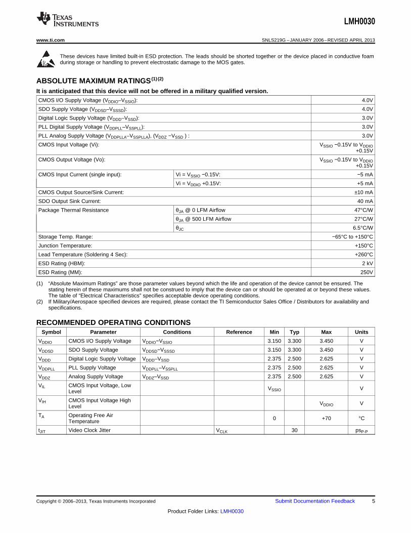
AC ELECTRICAL CHARACTERISTICSOver Supply Voltage and Operating Temperature ranges, unless otherwise specified (1).
Symbol Parameter Conditions Reference Min Typ Max Units
fVCLK Parallel Video Clock VCLK 27 74.25 MHzFrequency
DCV Video Clock Duty Cycle VCLK 45 50 55 %
fACLK Ancillary Clock Frequency ACLK VCLK MHz
DCA Ancillary Clock Duty ACLK 45 50 55 %Cycle
tr, tf Input Clock and Data Rise 10%–90% VCLK, ACLK, DVN, 1.0 1.5 3.0 nsTime, Fall Time ADN
BRSDO Serial Data Rate (2) (3)SDO, SDO 270 1,485 Mbps
tr, tf Rise Time, Fall Time 20%–80%, (3) SDO, SDO 270 ps
tr, tf Rise Time, Fall Time 20%–80%, (2) SDO, SDO 500 ps
Output Overshoot (4) SDO, SDO 5 %
(1) Typical values are stated for VDDIO = VDDSD = +3.3V, VDDD = VDDPLL = +2.5V and TA = +25°C.(2) RL = 75Ω, AC-coupled @ 270 Mbps, RREFLVL = RREFPRE = 4.75 kΩ 1%, See Test Loads and Test Circuit.(3) RL = 75Ω, AC-coupled @ 1,485 Mbps, RREFLVL = RREFPRE = 4.75 kΩ 1%, See Test Loads and Test Circuit.(4) Specification is ensured by design.
6 Submit Documentation Feedback Copyright © 2006–2013, Texas Instruments Incorporated
Product Folder Links: LMH0030
LMH0030
www.ti.com SNLS219G –JANUARY 2006–REVISED APRIL 2013
AC ELECTRICAL CHARACTERISTICS (continued)Over Supply Voltage and Operating Temperature ranges, unless otherwise specified(1).
Symbol Parameter Conditions Reference Min Typ Max Units
tj Serial Output Jitter, 270 Mbps,(2) (5) (6) (7) SDO, SDO 270 350 psP-PIntrinsic
tj Serial Output Jitter, 1,485 Mbps,(3) (5) (6) (7) SDO, SDO 85 125 psP-PIntrinsic
tLOCK Lock Time See (2) (8) (9)(SD Rates) 15 ms
tLOCK Lock Time See (3) (8) (9) (HD Rates) 15 ms
tS Setup Time, Video Data Timing Diagram, (4) DVN to VCLK 1.5 2.0 ns
tH Hold Time, Video Data Timing Diagram, (4) VCLK to DVN 1.5 2.0 ns
tS Setup Time, Anc. Data Timing Diagram, (4) ADN to ACLK 1.5 2.0 nsPort
tH Hold Time, Anc. Data Port Timing Diagram, (4) ACLK to ADN 1.5 2.0 ns
(5) Intrinsic timing jitter is measured in accordance with SMPTE RP 184-1996, SMPTE RP 192-1996 and the applicable serial datatransmission standard, SMPTE 259M-1997 or SMPTE 292M-1998. A color bar test pattern is used. The value of fSCLK is 270 MHz or360 MHz for SMPTE 259M, 540MHz for SMPTE 344M, or 1485 MHz for SMPTE 292M serial data rates. See Timing Jitter Bandpasssection.
(6) Intrinsic jitter is defined in accordance with SMPTE RP 184-1996 as: jitter at an equipment output in the absence of input jitter. Asapplied to this device, the input port is VCLK and the output port is SDO or SDO.
(7) Specification is ensured by characterization.(8) Measured from rising-edge of first DVCLK cycle until Lock Detect output goes high (true). Lock time includes format detection time plus
PLL lock time.(9) Average value measured between rising edges computed over at least one video field.
Copyright © 2006–2013, Texas Instruments Incorporated Submit Documentation Feedback 7
Product Folder Links: LMH0030

Jitter Frequency
Jitt
er
Ba
nd
pa
ss
10Hz >1/10 fSCLK
slopes:
20dB/decade
0dB
Passband ripple
< ±1dB
Stopband rejection
>20dB
75:1%
CL
SDO
SDO
75: test eqpt.(attenuation
0dB)
1.0PF
VDDSD
75:1%
CL
50: test eqpt.(attenuation
3.5dB)
1.0PF
24.9:1%
5.5-30pF*
* risetime
compensation
VDDSD
SDO
SDO
Hi-Z test eqpt. t 5k:(attenuation 0dB)
CL
CMOS
outputs
VDDIO
IOL
IOH
S2
S1
CL including probe and jig capacitance, 3pF max.
S1 - open, S2 - closed for VOH measurementS1 - closed, S2 - open for VOL measurement
LMH0030
SNLS219G –JANUARY 2006–REVISED APRIL 2013 www.ti.com
Test Loads
Timing Jitter Bandpass
8 Submit Documentation Feedback Copyright © 2006–2013, Texas Instruments Incorporated
Product Folder Links: LMH0030

1.0 PF
4.7 PF16V
4.75k1%
4.75k1%
1.0 PF
0.1 PF
75:1%
75:1%
4.7 PF16V
0.1 PF
(x3)(x3)
(x4)
(x4)
+3.3 Vdc
+2.5 Vdc
0 Vdc
+3.3V
+3.3V
44
42
41
40
39
38
36
35
34
12
13
14
15
18
19
20
21
22
23
24
25
26
27
28
29
30
31
32
33
11
9
8
7
6
5 4
3
10, 17, 43
16, 37
DV0
DV1
DV2
DV3
DV4
DV5
DV6
DV7
DV8
DV9
VCLK
SDO
VD
DS
D
VD
DZ
VD
DIO
RESET
LMH0030
48
47
46
45
DV10
DV11
DV12
DV13
DV14
DV15
DV16
DV17
DV18
DV19
AD0
AD1
AD2
AD3
AD4
AD5
AD6
AD7
AD8
AD9
ACLK
64
63
1
61
60
58
57
56
54, 55
53
52
51
50
49RD/WR
IO1
IO0
VS
SIO
VS
SD
VD
DD
ANC/CTRL
VD
DLS
IO2
IO3
IO4
IO5
IO6
IO7
RREFPRE
RREFLVL
SDO
VD
DP
LLD
VS
SP
LLA
VS
SS
D
2.5VSupply
3.3VSupply
2.5VSupply
3.3VSupply
HD Chroma,SD Luma &
Chroma
HD Luma
Output loads omitted for clarity.
VS
SLS
59
62
VD
DP
LLA
VS
SP
LLD
2
LMH0030
www.ti.com SNLS219G –JANUARY 2006–REVISED APRIL 2013
Test Circuit
Copyright © 2006–2013, Texas Instruments Incorporated Submit Documentation Feedback 9
Product Folder Links: LMH0030
tS
tH
VCLK
(ACLK)
DV[19:0]
(AD[9:0])
50%
90%
10%
90%
10%
90%
10%
tr, tf
tr, tf
LMH0030
SNLS219G –JANUARY 2006–REVISED APRIL 2013 www.ti.com
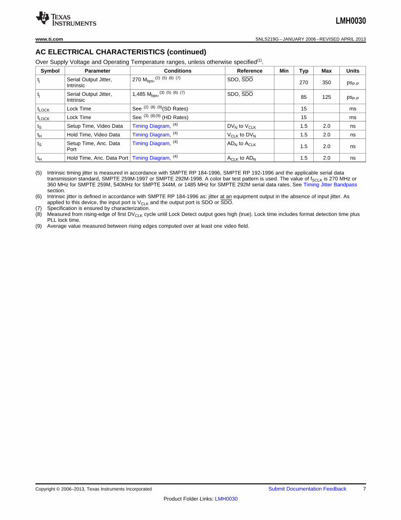
Timing Diagram
DEVICE OPERATION
The LMH0030 SDTV/HDTV Serializer is used in digital video signal origination equipment: cameras, video taperecorders, telecines and video test and other equipment. It converts parallel SDTV or HDTV component digitalvideo signals into serial format. Logic levels within this equipment are normally produced by LVCMOS logicdevices. The encoder produces serial digital video (SDV) signals conforming to SMPTE 259M, SMPTE 344M, orSMPTE 292M. The LMH0030 operates at parallel data rates of 27.0 MHz, 36.0 MHz, 54.0 MHz, 74.176MHz and74.25 MHz. Corresponding serial data rates are 270 Mbps, 360 Mbps, 540 Mbps, 1.4835 Gbps and 1.485 Gbps.
VIDEO DATA PATH
The input data register accepts 10-bit standard definition or 20-bit high definition parallel data and associatedparallel clock signals having LVCMOS-compatible levels. All parallel video data inputs, DV[19:0], have internalpull-down devices. VCLK does not have an internal pull-down device. Parallel video data may conform to any ofseveral SMPTE standards: 125M, 267M, 260M, 274M, 295M or 296M. Some segmented frame formats are notsupported. For HDTV data, the upper 10 bits of the DV input are luminance (luma) information and the lower 10bits are color difference (chrominance or chroma) information. For SDTV data, the lower order 10 bits containboth luma and chroma information. Output from this register feeds the video FIFO, video format detection circuit,TRS character detector, SMPTE scrambler, EDH/CRC generators, serializer/NRZI converter and the devicecontrol system.
Data from the input data register passes into a 4-register deep video FIFO prior to encoding and otherprocessing. The depth of this FIFO is set by the VIDEO FIFO Depth[2:0] bits of the ANC 0 control register.
The video format detector automatically determines the raster characteristics (video data format) of the parallelinput data and configures the LMH0030 to properly handle the data. This assures that the data will be properlyformatted, that the correct data rate is selected and that ancillary data, line numbers (HD) and CRC/EDH dataare correctly inserted. Indication of the standard being processed is stored in the FORMAT[4:0] bits in theFORMAT 1 control data register. This format data can be programmed for output on the multi-function I/O port.
The LMH0030 normally operates in an auto-format-detection mode. It may optionally be configured to processonly a single video format by writing the appropriate FORMAT SET[4:0] control data into the FORMAT 0 controlregister. The default state of FORMAT SET[4:0] is 0000b. Also, the LMH0030 may be configured to handle onlythe standard-definition data formats by setting the SD ONLY bit or only the high-definition data formats by settingthe HD ONLY bit in the FORMAT 0 control register. When both of these bits are reset the part automaticallyselects the data rate.
The TRS character detector processes the timing reference signals which control raster framing. The TRSdetector supplies control signals to the system controller to identify the presence of the valid video data. Thesystem controller supplies necessary control signals to the EDH/CRC control block. TRS character LSB-clippingas prescribed in ITU-R BT.601 is used. LSB-clipping causes all TRS characters with a value between 000h and003h to be forced to 000h and all TRS characters with a value between 3FCh and 3FFh to be forced to 3FFh.Clipping is done prior to scrambling and EDH/CRC character generation.
The LMH0030 incorporates circuitry for LSB dithering. The Dither Enable bit in the VIDEO INFO 0 registerwhen set enables dithering. The V Dither Enable bit in the VIDEO INFO 0 control register when set enablesdithering during the vertical blanking interval. The initial condition of Dither Enable and V Dither Enable is OFF.
10 Submit Documentation Feedback Copyright © 2006–2013, Texas Instruments Incorporated
Product Folder Links: LMH0030

LMH0030
www.ti.com SNLS219G –JANUARY 2006–REVISED APRIL 2013
The SMPTE scrambler accepts 10-bit standard definition or 20-bit high definition parallel video data andencodes it using the polynomial X9 + X4 + 1 as specified in the respective standard: SMPTE 259M, SMPTE344M, or SMPTE 292M. The data is then serialized and sent to the NRZ-to-NRZI converter before being output.The transmission bit order is LSB-first.
The NRZ-to-NRZI converter accepts NRZ serial data from the SMPTE scrambler. The data is converted to NRZIformat using the polynomial (X + 1). The converter's output goes to the output cable driver amplifier.
ANCILLARY/CONTROL DATA PATH
The 10-bit, bi-directional Ancillary and Control Data Port performs two distinct functions in the LMH0030. First,it is used to selectively load ancillary data into the Ancillary Data FIFO for insertion into the video data stream.The utilization and flow of ancillary data within the device is managed by a system of control bits, masks and IDsin the control data registers. Second, this port provides read/write access to contents of the configuration andcontrol registers.
Ancillary and control data are input via the 10-bit Ancillary/Control Data Port, AD[9:0]. The state of the RD/WRcontrol input determines whether data is read or written to the registers or written to the Ancillary Data FIFO. Thestate of the ANC/CTRL control input selects which of the ancillary data or control data sub-systems is accessedthrough the port.
The ACLK input controls data flow through the port. The operation and frequency of ACLK is independent of thevideo data clock, VCLK. However, the frequency of ACLK must be less than or equal to VCLK. There is no lowfrequency limit for ACLK when it is being used for control register access. When theANC/CTRL input is a logic-high, ACLK affects only the ancillary data FIFO operation. When the ANC/CTRL input is a logic-low, ACLKaffects only the control register operation.
Inputs AD[9:0], RD/WR and ANC/CTRL have internal pull down devices. ACLK does not have an internal pulldown device.
CONTROL DATA READ FUNCTIONS
Control data is written to and read from the LMH0030 using the lower-order 8 bits AD[7:0] of theAncillary/Control Data Port. This control data initializes, monitors and controls operation of the LMH0030. Theupper two bits AD[9:8] of the port are handshaking signals with the device accessing the port. AD[9:8] must bedriven as 00b (0XXh, where XX are AD[7:0]) when either a control register read or write address is being writtento the port. AD[9:8] must be driven as 11b (3XXh, where XX are AD[7:0]) when control data is being written tothe port. When control data is being read from the port, the LMH0030 will output AD[9:8] as 10b (2XXh, whereXX are output data AD[7:0]) and may be ignored by the monitoring system.
NOTEWhen power is first applied to the device or after it is reset, the Ancillary and ControlData Port must be initialized to receive data. This is done by toggling ACLK three (3)times.
Figure 2 shows the sequence of clock and control signals for reading control data from the ancillary/control dataport. The Control Data Read mode is entered by making the ANC/CTRL input low and the RD/WR input high.Next, the 8-bit address of the control register set to be accessed is placed on port bits AD[7:0]. When a controlregister read address is being written to the port, AD[9:8] must be driven as 00b (0XXh, where XX are AD[7:0]).ACLK is then toggled. The address is captured on the rising edge of ACLK. Observe the port input hold timingspecification.
Data from the selected register is driven by the port within a few nanoseconds immediately following the risingedge of ACLK. To avoid contention with the port, the address driver should be turned off or tri-statedimmediately after the address is clocked into the device. Data may be read by external devices at any time afterthe removal of the address signal. Output data will be driven until the next rising edge of ACLK. When the hostsystem finishes reading the data, toggle ACLK again. This second clock resets the port from drive to receivemode and readies the port for another access cycle. When control data is being read from the port, the LMH0030will output AD[9:8] as 10b (2XXh, where XX are output data AD[7:0]) and may be ignored by the monitoringsystem.
Copyright © 2006–2013, Texas Instruments Incorporated Submit Documentation Feedback 11
Product Folder Links: LMH0030

RD / WR
ANC / CTRL
ADDR DATA DATAADDR ADDR DATAAD[7:0]
WRITE
EXTERNAL BUS MUST
RELEASE
INTERNAL BUS WILL
RELEASE
ACLK
READ READ
AD[9:8]
AD[9]
AD[8]
DRIVEN REC'D DRIVEN REC'D DRIVEN DRIVEN
AD[9]
AD[8]AD[8]
AD[9]
AD[8]
AD[9:8]
LMH0030
SNLS219G –JANUARY 2006–REVISED APRIL 2013 www.ti.com
Example: Read the Full-field Flags via the AD port.1. Set ANC/CTRL to a logic-low.2. Set RD/WR to a logic-high.3. Present 001h to AD[9:0] as the register address.4. Toggle ACLK.5. Release the bus driving the AD port.6. Read the data present on the AD port. The Full-field Flags are bits AD[4:0].7. Toggle ACLK to release the AD port.
Figure 2. Control Data Read Timing (2 read and 1 write cycle shown)
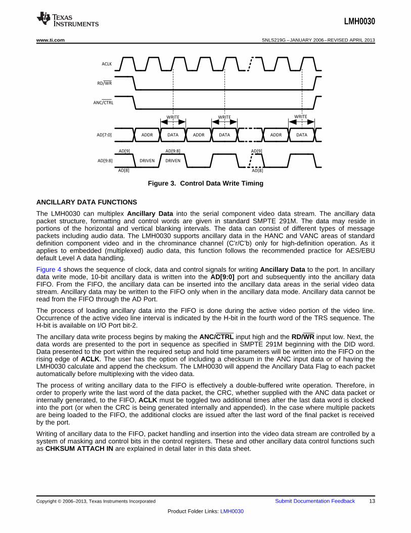
CONTROL DATA WRITE FUNCTIONS
Figure 3 shows the sequence of clock and control signals for writing control data to the ancillary/control data port.The control data write mode is similar to the read mode. The control data write mode is started by making boththe ANC/CTRL input low and the RD/WR input low. Next, the 8-bit address of the control register set to beaccessed is placed on port bits AD[7:0]. When a control register write address is being written to the port,AD[9:8] must be driven as 00b (0XXh, where XX are AD[7:0]). Toggle ACLK. The address is captured on therising edge of ACLK. Remove the address after clocking it into the device on or before the falling edge of ACLK.Observe the port input hold timing specification.
Next, the control register data is placed on the AD[7:0] port. ACLK is again toggled. The data is written to theselected register on the rising edge of ACLK. When control data is being written to the port, AD[9:8] must bedriven as 11b (3XXh, where XX are AD[7:0]). Remove the register data after clocking it into the device on orbefore the falling edge of ACLK. Observe the port input hold timing specification.
Example: Setup (without enabling) the TPG Mode via the AD port using the 1125 line, 30 frame, 74.25MHz,interlaced component (SMPTE 274M) color bars as test pattern. The TPG may be enabled after setup using theMulti-function I/O port or by the control registers.1. Set ANC/CTRL to a logic-low.2. Set RD/WR to a logic-low.3. Present 00Dh to AD[9:0] as the Test 0 register address.4. Toggle ACLK.5. Present 327h to AD[9:0] as the register data.6. Toggle ACLK.
12 Submit Documentation Feedback Copyright © 2006–2013, Texas Instruments Incorporated
Product Folder Links: LMH0030
ACLK
RD/WR
ANC/CTRL
ADDR DATA DATAADDR ADDR DATAAD[7:0]
AD[9:8]
AD[9]
AD[8]
DRIVEN
AD[9]
AD[8]
AD[9:8]
DRIVEN
WRITE WRITE WRITE
LMH0030
www.ti.com SNLS219G –JANUARY 2006–REVISED APRIL 2013
Figure 3. Control Data Write Timing
ANCILLARY DATA FUNCTIONS
The LMH0030 can multiplex Ancillary Data into the serial component video data stream. The ancillary datapacket structure, formatting and control words are given in standard SMPTE 291M. The data may reside inportions of the horizontal and vertical blanking intervals. The data can consist of different types of messagepackets including audio data. The LMH0030 supports ancillary data in the HANC and VANC areas of standarddefinition component video and in the chrominance channel (C’r/C’b) only for high-definition operation. As itapplies to embedded (multiplexed) audio data, this function follows the recommended practice for AES/EBUdefault Level A data handling.
Figure 4 shows the sequence of clock, data and control signals for writing Ancillary Data to the port. In ancillarydata write mode, 10-bit ancillary data is written into the AD[9:0] port and subsequently into the ancillary dataFIFO. From the FIFO, the ancillary data can be inserted into the ancillary data areas in the serial video datastream. Ancillary data may be written to the FIFO only when in the ancillary data mode. Ancillary data cannot beread from the FIFO through the AD Port.
The process of loading ancillary data into the FIFO is done during the active video portion of the video line.Occurrence of the active video line interval is indicated by the H-bit in the fourth word of the TRS sequence. TheH-bit is available on I/O Port bit-2.
The ancillary data write process begins by making the ANC/CTRL input high and the RD/WR input low. Next, thedata words are presented to the port in sequence as specified in SMPTE 291M beginning with the DID word.Data presented to the port within the required setup and hold time parameters will be written into the FIFO on therising edge of ACLK. The user has the option of including a checksum in the ANC input data or of having theLMH0030 calculate and append the checksum. The LMH0030 will append the Ancillary Data Flag to each packetautomatically before multiplexing with the video data.
The process of writing ancillary data to the FIFO is effectively a double-buffered write operation. Therefore, inorder to properly write the last word of the data packet, the CRC, whether supplied with the ANC data packet orinternally generated, to the FIFO, ACLK must be toggled two additional times after the last data word is clockedinto the port (or when the CRC is being generated internally and appended). In the case where multiple packetsare being loaded to the FIFO, the additional clocks are issued after the last word of the final packet is receivedby the port.
Writing of ancillary data to the FIFO, packet handling and insertion into the video data stream are controlled by asystem of masking and control bits in the control registers. These and other ancillary data control functions suchas CHKSUM ATTACH IN are explained in detail later in this data sheet.
Copyright © 2006–2013, Texas Instruments Incorporated Submit Documentation Feedback 13
Product Folder Links: LMH0030

ACLK
MULTIFUNCTION
I/O PORT BIT
ACLK
RD/WR
ANC/CTRL
AD[9:0]
WRITE
DATA DATA DATADATADATA DATA DATA
LMH0030
SNLS219G –JANUARY 2006–REVISED APRIL 2013 www.ti.com
Figure 4. Ancillary Data Write Timing
MULTI-FUNCTION I/O PORT
The Multi-function I/O port can be configured to provide immediate access to many control and indicatorfunctions within the LMH0030 configuration and control registers. The individual pins comprising this port may beassigned as input or output for selected bits in the control data registers. The multi-function I/O port is configuredby way of an 8x6-bit register bank, I/O pin 0 CONFIG through I/O pin 7 CONFIG. The pin configuration registerscontain codes which assign a control register bit to a particular I/O pin. Controls and indicators that areaccessible by the port and their corresponding selection addresses are given in the I/O Pin ConfigurationRegister Addresses, Table 6. Table 2 gives the control register bit assignments.
CAUTION
When writing data into the control registers via the multi-function I/O port, ACLK mustbe toggled to register the data as shown in Figure 5. It is not necessary to toggleACLK when reading data from the multi-function I/O port.
Example: Program multi-function I/O port bit-0 as the SAV bit output.1. Set ANC/CTRL to a logic-low.2. Set RD/WR to a logic-low.3. Present 00Fh to AD[9:0] as the I/O PIN 0 CONFIG register address (see Table 3).4. Toggle ACLK.5. Present 30Dh to AD[9:0] as the register data (see Table 6).6. Toggle ACLK.
Figure 5. I/O Port Data Write Timing
14 Submit Documentation Feedback Copyright © 2006–2013, Texas Instruments Incorporated
Product Folder Links: LMH0030

LMH0030
www.ti.com SNLS219G –JANUARY 2006–REVISED APRIL 2013
EDH/CRC SYSTEM
The LMH0030 has EDH and CRC character generation and insertion circuitry. The EDH system functions asdescribed in SMPTE Recommended Practice RP-165. The CRC system functions as specified in SMPTE 292M.The EDH/CRC polynomial generators accept parallel data from the input register and generate the EDH andCRC check words for insertion in the serial data. Incoming parallel data is checked for errors and the EDH flagsare updated automatically. EDH check words and status flags for SDTV data are generated using the polynomialX16 + X12 + X6 + 1 per SMPTE RP165. EDH check words are inserted in the serial data stream at the correctpositions in the ancillary data space and formatted per SMPTE 291M. Generation and automatic insertion of theEDH check words is controlled by EDH Force and EDH Enable bits in the control registers. After a reset, theinitial state of all EDH and CRC check characters is 00h.
The SMPTE 292M high definition video standard employs CRC (cyclic redundancy check codes) error checkinginstead of EDH. The CRC consists of two 18-bit words generated using the polynomial X18 + X5 + X4 + 1 perSMPTE 292M. One CRC is used for luminance and one for chrominance data. CRC data is inserted at therequired place in the video data according to SMPTE 292M. The CRCs appear in the data stream following theEAV and line number characters.
EDH and CRC errors are reported in the EDH0, EDH1, and EDH2 register sets of the configuration and controlregisters.
PHASE-LOCKED LOOP SYSTEM
The phase-locked loop (PLL) system generates the output serial data clock at 10x (standard definition) or 20x(high definition) the parallel data clock frequency. This system consists of a VCO, dividers, phase-frequencydetector and internal loop filter. The VCO free-running frequency is internally set. The parallel data clock VCLK isthe reference for the PLL. The PLL automatically generates the appropriate frequency for the serial clock rate.Loop filtering is internal to the LMH0030. The VCO has separate analog and digital power supply feeds: VDDPLLApin 62, VSSPLLA pin 61, VDDPLLD pin 1, and VSSPLLD pin 2. These may be separately supplied power via externallow-pass filters, if desired. PLL acquisition time is less than 200µs @ 1485 Mbps. The VCO halts when the VCLKsignal is not present or is inactive.
A LOCK DETECT indicator function is available as a bit in the VIDEO INFO 0 control registers. LOCK DETECTis a logic-1 when the PLL is locked and a valid format has been detected. It can be assigned as an output on themultifunction I/O port. By default LOCK DETECT is assigned as I/O Port bit 4 after power-on or reset . Thisfunction also includes logic to check the stability of the device after the digital logic reset is released followingPLL lock. If the system is not fully stable, the logic is automatically reset. LOCK DETECT also combines thefunction of indicating that the LMH0030 has detected the video format being received. This format detect functioninvolves determination of the major raster parameters such as line length, number of video lines in a frame, andso forth. This is done so that information like line numbering can be correctly inserted. The PLL itself will havelocked in 200 microseconds (HD rates) or less. However, resolution of all raster parameters may take themajority of a frame.
SERIAL DATA OUTPUT DRIVER
The serial data outputs provide low-skew complimentary or differential signals. The output buffer is a current-mode design and is intended to drive AC-coupled and terminated, 75Ω coaxial cables. The driver automaticallyadjusts its output slew rate depending upon the data rate being processed. Output levels are 800 mVP-P ±10%into 75Ω AC-coupled loads. The 75Ω resistors connected to the SDO outputs function both as drain-load andback-matching resistors. Series back-matching resistors are not used with this output type.
The serial output level is controlled by the value of RREFLVL and RREFPRE connected to pin 53 and pin 52,respectively. The RREFLVL resistor sets the peak-to-peak level of the output signal to the required SMPTEnominal level. The RREFPRE resistor sets the value of a pre-emphasis current which is active during thetransition times of the HD-rate output signal. The value of RREFLVL is normally 4.75 KΩ, ±1%. The value ofRREFPRE is normally 4.75 KΩ, ±1%. The voltage present at these pins is approximately +1.3Vdc. The transitiontimes of this output buffer design automatically adjust and are different for the HD and SD data rate conditions.The output buffer is quiescent when the device is in an out-of-lock condition. The output will become active afterthe PLL is locked and a valid format has been detected. Separate power feeds are provided for the serial outputdriver: VSSSD, pins 54, 55, and 59; VDDSD, pin 51; and VDDLS, pin 57.
Copyright © 2006–2013, Texas Instruments Incorporated Submit Documentation Feedback 15
Product Folder Links: LMH0030

LMH0030
SNLS219G –JANUARY 2006–REVISED APRIL 2013 www.ti.com
CAUTION
This output buffer is not designed or specified for driving 50Ω or other impedanceloads.
NOTEThe SMPTE return loss specification is highly dependent on board design and can bechallenging to meet with the LMH0030's integrated cable driver. In order to meet theSMPTE return loss specification, it is recommended to use an external cable driver suchas the LMH0002 HD/SD SDI cable driver on the output of the LMH0030.
POWER SUPPLIES, POWER-ON-RESET AND RESET INPUT
The LMH0030 requires two power supplies, 2.5V for the core logic functions and 3.3V for the I/O functions. Thesupplies must be applied to the device in proper sequence. The 3.3V supply must be applied prior to orcoincident with the 2.5V supply. Application of the 2.5V supply must not precede the 3.3V supply. It isrecommended that the 3.3V supply be configured or designed so as to control application of the 2.5V supply inorder to satisfy this sequencing requirement.
The LMH0030 has an automatic, power-on-reset circuit. Reset initializes the device and clears TRS detectioncircuitry, all latches, registers, counters and polynomial generators, sets the EDH/CRC characters to 00h anddisables the serial output. Table 1 lists the initial conditions of the configuration and control registers. An active-HIGH-true, manual reset input is available at pin 64. The reset input has an internal pull-down device and maybe considered inactive when unconnected.
Important: When power is first applied to the device or following a reset, the Ancillary and Control Data Portmust be initialized to receive data. This is done by toggling ACLK three times.
TEST PATTERN GENERATOR (TPG) AND BUILT-IN SELF-TEST (BIST)
The LMH0030 includes a built-in test pattern generator (TPG). Four test pattern types are available for all datarates, all HD and SD formats, NTSC and PAL standards, and 4x3 and 16x9 raster sizes. The test patterns are:flat-field black, PLL pathological, equalizer (EQ) pathological and a 75%, 8-color vertical bar pattern. Thepathologicals follow the recommendations of SMPTE RP 178-1996 regarding the test data used. The color barpattern has optional bandwidth limiting coding in the chroma and luma data transitions between bars. The VPGFILTER ENABLE bit in the VIDEO INFO 0 control register enables the color bar filter function. The defaultcondition of VPG FILTER ENABLE is OFF.
The TPG also functions as a built-in self-test (BIST) which can verify device functionality. The BIST functionperforms a comprehensive go/no-go test of the device. The test may be run using any of the HD color bar testpatterns or one of two SD test patterns, either a 270 Mbps NTSC full-field color bar or a PAL PLL pathological,as the test data pattern. Data is supplied internally in the input data register, processed through the device andtested for errors using either the EDH system for SD or the CRC system for HD. A go/no-go indication is loggedin the Pass/Fail bit of the TEST 0 control register set. This bit may be assigned as an output on the multifunctionI/O port.
TPG and BIST operation is initiated by loading the code for the desired test pattern into the Test Pattern Select[5:0] bits of the TEST 0 register. Table 5 gives the available test patterns and codes. (Recall also therequirement to initialize the ancillary data port control logic by clocking ACLK at least three (3) complete cyclesbefore attempting to load the first register address). In the default power-on state, TPG Enable appears as bit 7on the multi-function I/O port. The TPG is run by applying the appropriate frequency at the VCLK input for theformat and rate selected and then setting the TPG Enable input on the multi-function I/O port, or by setting theTPG Enable bit in the TEST 0 register.
Important: If the TPG Enable input of the I/O port is in its default mapping and is not being used to enable theTPG mode, attempting to enable TPG operation by setting bit 6 of the TEST 0 register will not cause the TPG tooperate. This is because the low logic level at the I/O port input pulldown overrides the high level being written tothe register. The result is the TPG does not run.
16 Submit Documentation Feedback Copyright © 2006–2013, Texas Instruments Incorporated
Product Folder Links: LMH0030

LMH0030
www.ti.com SNLS219G –JANUARY 2006–REVISED APRIL 2013
The Pass/Fail bit in the TEST 0 control register indicates the test status. If no errors have been detected, this bitwill be set to logic-1 approximately 2 field intervals after TPG Enable is set. If errors have been detected in theinternal circuitry of the LMH0030, Pass/Fail will remain reset to a logic-0. The TPG or BIST is halted by resettingTPG Enable. The serial output data is present at the SDO outputs during TPG or BIST operation.
CAUTION
When attempting to use the TPG or BIST immediately after applying power or resettingthe device, the TPG defaults to the 270 Mbps SD rate and expects a VCLK clockfrequency of 27MHz as input. This is because the code for the test pattern in the TEST0 register is set to 00h (525 line, 30 frame, 27MHz, NTSC 4x3 reference black).Attempting to apply a VCLK frequency higher than the device expects, according to thesetting in the TEST 0 register, may result in the PLL locking up while attempting toslew to its maximum possible frequency. This situation is not recoverable by the use ofthe device RESET input. To recover from this condition, power must be removed andre-applied to the device. Proper conditioning of the VCLK input, which does not have aninternal pull down device, is mandatory to prevent admission of noise or unwantedsignals at any time, especially during power-up or reset sequences. It is stronglyrecommended that VCLK not be applied until device initialization and configuration iscompleted.
Example: Enable the TPG Mode to use the NTSC 270 Mbps color bars as the BIST and TPG pattern. EnableTPG operation using the I/O port.1. Set ANC/CTRL to a logic-low.2. Set RD/WR to a logic-low.3. Present 00Dh to AD[9:0] as the TEST 0 register address.4. Toggle ACLK.5. Present 303h to AD[9:0] as the register data (525 line, 30 frame, 27MHz, NTSC 4x3, color bars (SMPTE
125M)).6. Toggle ACLK.7. Set TPG ENABLE (I/O Port, bit 7) to a logic-high.8. Toggle ACLK.9. The PASS/FAIL indicator (I/O Port, bit 6) is monitored for the result of the test. Alternatively, the TEST 0
register may be read. Bit 7 is the Pass/Fail indicator bit.
CONFIGURATION AND CONTROL REGISTERS
The configuration and control registers store data which configures the operational modes of the LMH0030 orwhich result from its operation. Many of these registers can be mapped to the multi-function I/O bus to makethem available as external I/O functions. These functions and initial values are summarized in Table 1 anddetailed in Table 2. The power-on default condition for the multi-function I/O port is indicated in Table 1 anddetailed in Table 6.
Table 1. Configuration and Control Data Register Summary
Assignable toRegister Function Bits Read or Write Initial Condition (1) NotesI/O Bus as
EDH Error (SD) 1 R Output See (1)
Full-Field Flags 5 R Reset No
Active Picture Flags 5 R Reset No
ANC Flags 5 R Reset No
EDH Force 1 R/W OFF Input
EDH Enable 1 R/W ON Input
F/F Flag Error 1 R Reset Output
(1) ON = logic-1, OFF = logic-0 (positive logic).
Copyright © 2006–2013, Texas Instruments Incorporated Submit Documentation Feedback 17
Product Folder Links: LMH0030

LMH0030
SNLS219G –JANUARY 2006–REVISED APRIL 2013 www.ti.com
Table 1. Configuration and Control Data Register Summary (continued)
Assignable toRegister Function Bits Read or Write Initial Condition (1) NotesI/O Bus as
A/P Flag Error 1 R Reset Output
ANC Flag Error 1 R Reset Output
ANC Checksum 1 R/W OFF InputForce
ANC Checksum Error 1 R Reset Output
FIFO Empty 1 R Set Output
FIFO Full 1 R Reset Output
FIFO Overrun 1 R Reset Output
Video FIFO Depth 3 R/W 000b No
ANC ID 16 R/W 0000h No
ANC Mask 16 R/W FFFFh No
FIFO Flush Static 1 R/W OFF No
Chksum Attach In 1 R/W OFF Input
FIFO Insert Enable 1 R/W OFF Input
ANC Parity Mask 1 R/W OFF NoDisable
VANC 1 R/W OFF No
Switch Point 0 8 R/W 00h No
Switch Point 1 8 R/W 00h No
Switch Point 2 8 R/W 00h No
Switch Point 3 8 R/W 00h No
Format Set 5 R/W OFF No
SD Only 1 R/W OFF No
HD Only 1 R/W OFF No
Format 5 R Output Format [4] (2)
H 1 R Output See (2)
V 1 R Output See (2)
F 1 R Output See (2)
Test Pattern Select 6 R/W 00000b Input 525/27 MHz/Black
TPG Enable 1 R/W OFF Input See (2)
Pass/Fail 1 R Output See (2)
New Sync Position 1 R Output(NSP)
SAV 1 R Output
EAV 1 R Output
Lock Detect 1 R Output See (2)
VPG Filter Enable 1 R/W OFF Input
Dither_Enable 1 R/W OFF Input
Vert. Dither Enable 1 R/W OFF No
Scrambler_ Enable 1 R/W ON No
NRZI_Enable 1 R/W ON No
LSB_Clipping 1 R/W ON No
SYNC_Detect_Enabl 1 R/W ON Noe
I/O Bus Pin Config. 48 R/W See Table 6 No
(2) Connected to multifunction I/O port at power-on.
18 Submit Documentation Feedback Copyright © 2006–2013, Texas Instruments Incorporated
Product Folder Links: LMH0030

LMH0030
www.ti.com SNLS219G –JANUARY 2006–REVISED APRIL 2013
Table 2. Control Register Bit Assignments
Bit 7 Bit 6 Bit 5 Bit 4 Bit 3 Bit 2 Bit 1 Bit 0
EDH 0 (register address 01h)
EDH ERROR EDH FORCE EDH ENABLE F/F FLAGS(4) F/F FLAGS(3) F/F FLAGS(2) F/F FLAGS(1) F/F FLAGS(0)(SD)
EDH 1 (register address 02h)
reserved reserved reserved A/P FLAGS(4) A/P FLAGS(3) A/P FLAGS(2) A/P FLAGS(1) A/P FLAGS(0)
EDH 2 (register address 03h)
F/F FLAG A/P FLAG ANC FLAG ANC ANC ANCANC FLAGS(3) ANC FLAGS(1)ERROR ERROR ERROR FLAGS(4) FLAGS(2) FLAGS(0)
ANC 0 (register address 04h)
VIDEO FIFO VIDEO FIFO VIDEO FIFO FIFO FIFO FIFO ANC CHECK- ANC CHECK-DEPTH(2) DEPTH(1) DEPTH(0) OVERRUN EMPTY FULL SUM ERROR SUM FORCE
ANC 1 (register address 05h) DID
ANC ID(7) ANC ID(6) ANC ID(5) ANC ID(4) ANC ID(3) ANC ID(2) ANC ID(1) ANC ID(0)
ANC 2 (register address 06h) SDID/DBN
ANC ID(15) ANC ID(14) ANC ID(13) ANC ID(12) ANC ID(11) ANC ID(10) ANC ID(9) ANC ID(8)
ANC 3 (register address 07h) DID
ANC MASK(7) ANC MASK(6) ANC MASK(5) ANC MASK(4) ANC MASK(3) ANC MASK(2) ANC MASK(1) ANC MASK(0)
ANC 4 (register address 08h) SDID/DBN
ANC ANC ANCANC MASK(15) ANC MASK(13) ANC MASK(11) ANC MASK(9) ANC MASK(8)MASK(14) MASK(12) MASK(10)
ANC 5 (register address 17h)
FIFO INSERT CHSUM FIFO FLUSHreserved reserved reserved reserved reservedENABLE ATTACH IN STATIC
ANC 6 (register address 18h)
ANC PARITYreserved reserved reserved reserved reserved reserved VANCMASK
SWITCH POINT 0 (register address 09h)
LINE(7) LINE(6) LINE(5) LINE(4) LINE(3) LINE(2) LINE(1) LINE(0)
SWITCH POINT 1 (register address 0Ah)
PROTECT(4) PROTECT(3) PROTECT(2) PROTECT(1) PROTECT(0) LINE(10) LINE(9) LINE(8)
SWITCH POINT 2 (register address 19h)
LINE(7) LINE(6) LINE(5) LINE(4) LINE(3) LINE(2) LINE(1) LINE(0)
SWITCH POINT 3 (register address 1Ah)
PROTECT(4) PROTECT(3) PROTECT(2) PROTECT(1) PROTECT(0) LINE(10) LINE(9) LINE(8)
FORMAT 0 (register address 0Bh)
FORMAT FORMAT FORMAT FORMAT FORMATreserved SD ONLY HD ONLY SET(4) SET(3) SET(2) SET(1) SET(0)
FORMAT 1 (register address 0Ch)
F V H FORMAT(4) FORMAT(3) FORMAT(2) FORMAT(1) FORMAT(0)
TEST 0 (register address 0Dh)
TEST TEST TEST TEST TEST TESTPASS/FAIL TPG ENABLE PATTERN PATTERN PATTERN PATTERN PATTERN PATTERN
SELECT(5) SELECT(4) SELECT(3) SELECT(2) SELECT(1) SELECT(0)
VIDEO INFO 0 (register address 0Eh)
VERT.DITHER VPG FILTER LOCKDITHER EAV SAV NSP reservedENABLE ENABLE DETECTENABLE
MULTI-FUNCTION I/O BUS PIN CONFIGURATION
I/O PIN 0 CONFIG (register address 0Fh)
reserved reserved PIN 0 SEL[5] PIN 0 SEL[4] PIN 0 SEL[3] PIN 0 SEL[2] PIN 0 SEL[1] PIN 0 SEL[0]
I/O PIN 1 CONFIG (register address 10h)
Copyright © 2006–2013, Texas Instruments Incorporated Submit Documentation Feedback 19
Product Folder Links: LMH0030

LMH0030
SNLS219G –JANUARY 2006–REVISED APRIL 2013 www.ti.com
Table 2. Control Register Bit Assignments (continued)
Bit 7 Bit 6 Bit 5 Bit 4 Bit 3 Bit 2 Bit 1 Bit 0
reserved reserved PIN 1 SEL[5] PIN 1 SEL[4] PIN 1 SEL[3] PIN 1 SEL[2] PIN 1 SEL[1] PIN 1 SEL[0]
I/O PIN 2 CONFIG (register address 11h)
reserved reserved PIN 2 SEL[5] PIN 2 SEL[4] PIN 2 SEL[3] PIN 2 SEL[2] PIN 2 SEL[1] PIN 2 SEL[0]
I/O PIN 3 CONFIG (register address 12h)
reserved reserved PIN 3 SEL[5] PIN 3 SEL[4] PIN 3 SEL[3] PIN 3 SEL[2] PIN 3 SEL[1] PIN 3 SEL[0]
I/O PIN 4 CONFIG (register address 13h)
reserved reserved PIN 4 SEL[5] PIN 4 SEL[4] PIN 4 SEL[3] PIN 4 SEL[2] PIN 4 SEL[1] PIN 4 SEL[0]
I/P PIN 5 CONFIG (register address 14h)
reserved reserved PIN 5 SEL[5] PIN 5 SEL[4] PIN 5 SEL[3] PIN 5 SEL[2] PIN 5 SEL[1] PIN 5 SEL[0]
I/O PIN 6 CONFIG (register address 15h)
reserved reserved PIN 6 SEL[5] PIN 6 SEL[4] PIN 6 SEL[3] PIN 6 SEL[2] PIN 6 SEL[1] PIN 6 SEL[0]
I/O PIN 7 CONFIG (register address 16h)
reserved reserved PIN 7 SEL[5] PIN 7 SEL[4] PIN 7 SEL[3] PIN 7 SEL[2] PIN 7 SEL[1] PIN 7 SEL[0]
TEST MODE 0 (register address 55h)
SYNC DETECT LSB SCRAMBLERreserved reserved reserved NRZI ENABLE reservedENABLE CLIPPING ENABLE
Table 3. Control Register Addresses
Address AddressRegister Name Decimal Hexadecimal
EDH 0 1 01
EDH 1 2 02
EDH 2 3 03
ANC 0 4 04
ANC 1 5 05
ANC 2 6 06
ANC 3 7 07
ANC 4 8 08
ANC 5 23 17
ANC 6 24 18
SWITCH POINT 0 9 09
SWITCH POINT 1 10 0A
SWITCH POINT 2 25 19
SWITCH POINT 3 26 1A
FORMAT 0 11 0B
FORMAT 1 12 0C
TEST 0 13 0D
VIDEO INFO 0 14 0E
I/O PIN 0 CONFIG 15 0F
I/O PIN 1 CONFIG 16 10
I/O PIN 2 CONFIG 17 11
I/O PIN 3 CONFIG 18 12
I/O PIN 4 CONFIG 19 13
I/O PIN 5 CONFIG 20 14
I/O PIN 6 CONFIG 21 15
I/O PIN 7 CONFIG 22 16
TEST MODE 0 85 55
20 Submit Documentation Feedback Copyright © 2006–2013, Texas Instruments Incorporated
Product Folder Links: LMH0030
LMH0030
www.ti.com SNLS219G –JANUARY 2006–REVISED APRIL 2013
EDH REGISTERS 0, 1 AND 2 (Addresses 01h through 03h)
Updated EDH packets may be inserted into the serial output data by setting the EDH Force bit in the controlregisters. The EDH Force control bit causes the insertion of new EDH checkwords and flags into the serialoutput regardless of the previous condition of EDH checkwords and flags in the input parallel data. This functionmay be used in situations where video content has been editted thus making the previous EDH informationinvalid. In the case of SMPTE 292M data, the CRC check characters are recalculated and inserted automaticallyregardless of the presence of CRC characters in the parallel data. After the LMH0030 is reset, the initial state ofthe CRC check characters is 00h.
The EDH Enable bit enables operation of the EDH generator function.
The EDH ERROR (SD) bit when set indicates that EDH error conditions are being reported in EDH ancillary datapackets present in the parallel input data. Details of the specific error conditions contained in the EDH packetsare reported via the full field, active picture and ancillary flag error bits and the specific flag bits in these registers.
The EDH flags F/F FLAGS[4:0] (full field), A/P FLAGS[4:0] (active picture) and ANC FLAGS[4:0] (ancillarydata) are defined in SMPTE RP 165. The EDH flags are stored in the control registers. The flags are updatedautomatically when the EDH function is enabled and data is being received.
The status of EDH flag errors in incoming SD parallel data are reported in the ffFlagError, apFlagError andancFlagError bits. The ffFlagError, apFlagError and ancFlagError bits are the logical-OR of the correspondingEDH and EDA flags of the EDH checkwords.
ANC REGISTER 0 (Address 04h)
The V FIFO Depth[2:0] bits control the depth of the video FIFO which follows the input data latches. The depthcan be set from 0 to 4 stages deep by writing the corresponding binary code into these bits. For example: to setthe Video FIFO depth at two registers, load 11010XXXXXb into the ANC 0 control register (where X representsthe other functional bits of this register). To retain other data previously stored in a register, read the register’scontents and logically-OR this with the new data. Then write the composite data back into the register.
Flags for FIFO EMPTY, FIFO FULL and FIFO OVERRUN are available in the configuration and control registerset. These flags can also be assigned as inputs and outputs on the multi-function I/O port. The FIFO OVERRUNflag indicates that an attempt to write data into a full FIFO has occurred.
The ANC Checksum Force bit, under certain conditions, enables the overwriting of ancillary data checksumsreceived in the parallel ancillary data. Calculation and insertion of new ancillary data checksums is controlled bythe ANC Checksum Force bit. If a checksum error is detected (calculated and received checksums do notmatch) and the ANC Checksum Force bit is set, a new checksum will be inserted in the ancillary data replacingthe previous one. If a checksum error is detected and the ANC Checksum Force bit is not set, the checksummismatch is reported via the ANC Checksum Error bit.
Ancillary data checksums may be received in the incoming parallel ancillary data. Alternatively they may becalculated and inserted automatically by the LMH0030. The CHKSUM ATTACH IN bit in the control registerswhen set to a logic-1 indicates that the checksum is to be supplied in the incoming data. When the CHKSUMATTACH IN bit is set, checksums for incoming data are calculated and checked against received checksums.Calculation and insertion of new ancillary data checksum is controlled by the ANC Checksum Force bit in theconfiguration and control registers. If a checksum error is detected (calculated and received checksums do notmatch) and the ANC Checksum Force bit is set, a new checksum will be inserted in the ancillary data replacingthe previous one. If a checksum error is detected and the ANC Checksum Force bit is not set, the checksummismatch is reported via the ANC CHECKSUM ERROR bit in the control registers.
The ANC Checksum Error bit indicates that the received ancillary data checksum did not agree with theLMH0030's internally generated checksum. This bit is available as an output on the multifunction I/O port.
ANC REGISTERS 1 THROUGH 4 (Address 05h through 08h)
Admission of ancillary data packets into the FIFO can be controlled by the ANC MASK[15:0] and ANC ID[15:0]bits in the control registers. The ANC ID[7:0] register can be set to a valid 8-bit Data Identification (DID) codeused for component ancillary data packet identification as specified in SMPTE 291M. Similarly, theANC ID[15:8]register can be set to a valid 8-bit Secondary Data Identification (SDID) or Data Block Number (DBN) code. TheANC MASK[7:0] is an 8-bit word that can be used to selectively control loading of packets with specific DIDs (orDID ranges) into the FIFO. Similarly, the ANC MASK[15:8] is an 8-bit word that can be used to selectivelycontrol loading of packets with specific SDID or DBNs (or SDID or DBN ranges).
Copyright © 2006–2013, Texas Instruments Incorporated Submit Documentation Feedback 21
Product Folder Links: LMH0030

LMH0030
SNLS219G –JANUARY 2006–REVISED APRIL 2013 www.ti.com
When ANC MASK[7:0] or ANC MASK[15:8] is set to FFh, packets with any DID, SDID or DBN can be loadedinto the FIFO. When any bit or bits of ANC MASK[7:0] or ANC MASK[15:8] are set to a logic-1, thecorresponding bit or bits of ANC ID[7:0] or ANC ID[15:8], respectively are a don't-care when matching IDs ofincoming packets. When ANC MASK[7:0] or ANC MASK[15:8] is set to 00h, the DID, SDID or DBN of incomingpackets must match exactly, bit-for-bit, the setting of ANC ID[7:0] or ANC ID[15:8] in the control register for thepackets to be loaded into the FIFO. The initial value of ANC MASK[7:0] and ANC MASK[15:8] is FFh. The initialvalue of ANC ID[7:0] and ANC ID[15:8] is 00h.
Bits 7 through 0 of Register ANC 1, ANC ID[7:0], and Register ANC3, ANC MASK[7:0], affect DID[7:0]. BIts 7through 0 of Register ANC2, ANC ID[15:8], and Register ANC 4, ANC MASK[15:8], affect SDID[7:0] orDBN[7:0].
ANC REGISTER 5 (Address 17h)
The FIFO INSERT ENABLE bit enables insertion of ancillary data stored in the FIFO into the serial data stream.Data insertion is enabled when this bit is set to a logic-1. This bit can be used to delay automatic insertion of datainto the serial data stream.
Setting the FIFO FLUSH STAT bit to a logic-1 flushes the FIFO. Data may not be loaded into the FIFO duringFIFO FLUSH STAT execution. Similarly, FIFO FLUSH STAT may not be set when data is being input to theFIFO. FIFO FLUSH STAT is automatically reset after this operation is complete. Execution of these FIFOoperations requires toggling of ACLK.
ANC REGISTER 6 (Addresses 18h)
The ANC PARITY MASK bit when set disables parity checking for the DATA ID (DID) and SECONDARY DATAID (SDID) or Data Block Number (DBN) in the ANC data packet. When reset, parity checking is enabled, and, if aparity error occurs, the packet will not be loaded.
The VANC bit in the control registers, when set to a logic-1, enables insertion of ancillary data during the verticalblanking interval.
SWITCH POINT REGISTERS 0 THROUGH 3 (Addresses 09h, 0Ah, 19h and 1Ah)
The Line[10:0] and Protect[4:0] bits define the vertical switching point line and number of protected linesfollowing the switching point line for fields 0 and 1 (or fields 1 and 2 as these are sometimes referred to) of high-defination formats. The vertical switching point for component digital standard definition formats is defined inSMPTE RP 168-1993. The vertical switching point for high-definition formats has the same basic definition.However, since the vertical switching point lines are not necessarily standardized among the various high-definition rasters, these registers provide a convenient means whereby the vertical switching point line andsubsequent protected lines may be specified by the user. The Switch Point registers do not operate for standarddefinition formats.
The Line[10:0] bits of registers Switch Point 0 and 1 may be loaded with a line number ranging from 0 to 1023which then specifies the switching point line for Field 0. The Protect[4:0] bits of register Switch Point 1determine the number of lines from 0 to 15 after the vertical switching point line in which ancillary data may notbe inserted. LINE(0) is the LSB and LINE(10) is the MSB for the Line[10:0] bits. Similar ordering holds for theProtect[4:0] bits.
The Line[10:0] and Protect[4:0] bits of registers Switch Point 2 and 3 perform the same function as explainedabove for the vertical switching point line for Field 1.
FORMAT REGISTERS 0 (Addresses 0Bh)
The LMH0030 may be set to process a single video format by writing the appropriate data into the FORMAT 0register. The Format Set[4:0] bits confine the LMH0030 to recognize and process only one of the fourteenspecified types of standard or high definition formats. When the LMH0030 is set to process a single format, it willnot recognize and therefore will not process other formats that it is capable of recognizing. The Format Set[4:0]bits may not be used to confine device operation to a range of standards. For normal operating situations, it isrecommended that the LMH0030 be operated in automatic format detection mode, i.e. that the Format 0 registerbe set to 00h.
22 Submit Documentation Feedback Copyright © 2006–2013, Texas Instruments Incorporated
Product Folder Links: LMH0030
LMH0030
www.ti.com SNLS219G –JANUARY 2006–REVISED APRIL 2013
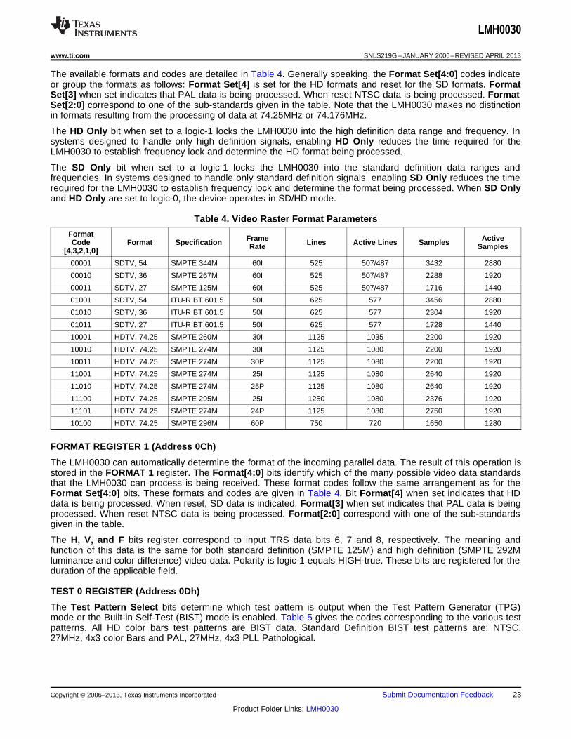
The available formats and codes are detailed in Table 4. Generally speaking, the Format Set[4:0] codes indicateor group the formats as follows: Format Set[4] is set for the HD formats and reset for the SD formats. FormatSet[3] when set indicates that PAL data is being processed. When reset NTSC data is being processed. FormatSet[2:0] correspond to one of the sub-standards given in the table. Note that the LMH0030 makes no distinctionin formats resulting from the processing of data at 74.25MHz or 74.176MHz.
The HD Only bit when set to a logic-1 locks the LMH0030 into the high definition data range and frequency. Insystems designed to handle only high definition signals, enabling HD Only reduces the time required for theLMH0030 to establish frequency lock and determine the HD format being processed.
The SD Only bit when set to a logic-1 locks the LMH0030 into the standard definition data ranges andfrequencies. In systems designed to handle only standard definition signals, enabling SD Only reduces the timerequired for the LMH0030 to establish frequency lock and determine the format being processed. When SD Onlyand HD Only are set to logic-0, the device operates in SD/HD mode.
Table 4. Video Raster Format Parameters
Format Frame ActiveCode Format Specification Lines Active Lines SamplesRate Samples[4,3,2,1,0]
00001 SDTV, 54 SMPTE 344M 60I 525 507/487 3432 2880
00010 SDTV, 36 SMPTE 267M 60I 525 507/487 2288 1920
00011 SDTV, 27 SMPTE 125M 60I 525 507/487 1716 1440
01001 SDTV, 54 ITU-R BT 601.5 50I 625 577 3456 2880
01010 SDTV, 36 ITU-R BT 601.5 50I 625 577 2304 1920
01011 SDTV, 27 ITU-R BT 601.5 50I 625 577 1728 1440
10001 HDTV, 74.25 SMPTE 260M 30I 1125 1035 2200 1920
10010 HDTV, 74.25 SMPTE 274M 30I 1125 1080 2200 1920
10011 HDTV, 74.25 SMPTE 274M 30P 1125 1080 2200 1920
11001 HDTV, 74.25 SMPTE 274M 25I 1125 1080 2640 1920
11010 HDTV, 74.25 SMPTE 274M 25P 1125 1080 2640 1920
11100 HDTV, 74.25 SMPTE 295M 25I 1250 1080 2376 1920
11101 HDTV, 74.25 SMPTE 274M 24P 1125 1080 2750 1920
10100 HDTV, 74.25 SMPTE 296M 60P 750 720 1650 1280
FORMAT REGISTER 1 (Address 0Ch)
The LMH0030 can automatically determine the format of the incoming parallel data. The result of this operation isstored in the FORMAT 1 register. The Format[4:0] bits identify which of the many possible video data standardsthat the LMH0030 can process is being received. These format codes follow the same arrangement as for theFormat Set[4:0] bits. These formats and codes are given in Table 4. Bit Format[4] when set indicates that HDdata is being processed. When reset, SD data is indicated. Format[3] when set indicates that PAL data is beingprocessed. When reset NTSC data is being processed. Format[2:0] correspond with one of the sub-standardsgiven in the table.
The H, V, and F bits register correspond to input TRS data bits 6, 7 and 8, respectively. The meaning andfunction of this data is the same for both standard definition (SMPTE 125M) and high definition (SMPTE 292Mluminance and color difference) video data. Polarity is logic-1 equals HIGH-true. These bits are registered for theduration of the applicable field.
TEST 0 REGISTER (Address 0Dh)
The Test Pattern Select bits determine which test pattern is output when the Test Pattern Generator (TPG)mode or the Built-in Self-Test (BIST) mode is enabled. Table 5 gives the codes corresponding to the various testpatterns. All HD color bars test patterns are BIST data. Standard Definition BIST test patterns are: NTSC,27MHz, 4x3 color Bars and PAL, 27MHz, 4x3 PLL Pathological.
Copyright © 2006–2013, Texas Instruments Incorporated Submit Documentation Feedback 23
Product Folder Links: LMH0030
LMH0030
SNLS219G –JANUARY 2006–REVISED APRIL 2013 www.ti.com
The TPG Enable bit when set to a logic-1 enables the Test Pattern Generator function and built-in self-test(BIST). This bit is mapped to I/O port bit 7 in the default condition. Note that the input pulldown on the I/O port bithas the effect of overriding the logic level of data being written into the register via the ancillary/Control DataPort. In cases where it is desired to control the state of TPG Enable through the control register instead of themulti-function I/O port, bit 7, the I/O port bit must be remapped to another bit in the control registers. Remappingto a read-only function is recommended to avoid possible conflicting data being written into the remappedlocation.
The Pass/Fail bit indicates the result of running the built-in self-test. This bit is a logic-1 for a pass condition. Thebit is mapped to I/O port bit 6 in the default condition.
VIDEO INFO 0 REGISTER (Address 0Eh)
The NSP (New Sync Position) bit indicates that a new or out-of-place TRS character has been detected in theinput data. This bit is set to a logic-1 and remains set for at least one horizontal line period or unless re-activatedby a subsequent new or out-of-place TRS. It is reset by an EAV TRS character.
The EAV (end of active video) and SAV (start of active video) bits track the occurrence of the correspondingTRS characters.
Lock Detect is registered as a control signal and is a logic-1 when the PLL is locked and a valid format has beendetected. This bit may be programmed as an output on the multi-function I/O port. This bit is mapped to I/O portbit 4 in the default condition. This function also includes logic to check the stability of the device after the digitallogic reset is released following PLL lock. If the system is not fully stable, the logic is automatically reset. LOCKDETECT also combines the function of indicating that the LMH0030 has detected the video format beingreceived. This format detect function involves determination of the major raster parameters such as line length,number of video lines in a frame, and so forth. This is done so that information like line numbering can becorrectly inserted. The PLL itself will have locked in about 50 microseconds (HD rates, 150 microseconds for SD)or less; however, resolution of all raster parameters may take the majority of a frame.
The VPG Filter Enable bit when set enables operation of the Video Pattern Generator filter. Operation of thisfilter causes the insertion of transition codes in the chroma and luma data of color bar test patterns where thesepatterns change from one bar to the next. This filter reduces the magnitude of out-of-band frequency productswhich can be produced by abrupt transitions in the chroma and luma data when fed to D-to-A converters andpicture monitors. The default condition of this bit is reset (off).
A method by which the occurrence of pathological data patterns can be prevented has been proposed for SDformats. The LMH0030 implements this process for SD formats. The Dither Enable and Vertical Dither Enablebits control operation of pseudo-random dithering applied to the two LSBs of the video data. Dithering is appliedto active video data when the Dither Enable bit is set. When the Vertical Dither Enable bit is set, dithering isapplied to that portion of the video line corresponding to active video for lines in the vertical blanking interval.
I/O PIN 0 THROUGH 7 CONFIGURATION REGISTERS (Addresses 0Fh through 16h)
The Multi-function I/O Bus Pin Configuration registers are used to map the bits of the multi-function I/O port toselected bits of the Configuration and Control Registers. Table 6 details the available Configuration and Controlregister bit functions that may be mapped to the port and their corresponding mapping addresses. Pin # SEL[5]in each register indicates whether the port pin is input or output. The port pin will be an input when this bit is setand an output when reset. Input-only functions may not be configured as outputs and vice versa. The remaininglower-order five address bits distinguish the particular function.
Example: Program, via the AD port, I/O port bit 0 as output for the SAV bit in the control registers.1. Set ANC/CTRL to a logic-low.2. Set RD/WR to a logic-low.3. Present 00Fh to AD[9:0] as the I/O PIN 0 CONFIG register address (see Table 3).4. Toggle ACLK.5. Present 30Dh to AD[9:0] as the register data, the bit address of the SAV bit in the control registers (see
Table 6).6. Toggle ACLK.
24 Submit Documentation Feedback Copyright © 2006–2013, Texas Instruments Incorporated
Product Folder Links: LMH0030
LMH0030
www.ti.com SNLS219G –JANUARY 2006–REVISED APRIL 2013
TEST MODE 0 REGISTER (Address 55h)
The four bits of this register are intended for use as test mode functions. They are not normal operating modes.The bits may be set (enabled) or reset (disabled) by writing to the register. Reading this register sets (enables)all bits to their default ON condition.
The Scrambler_Enable bit enables operation of the SMPTE scrambler function. This bit is normally ON.
The NRZI_Enable bit enables operation of the NRZ-to-NRZI conversion function. This bit is normally ON.
The LSB_Clipping bit enables operation of the LSB clipping function. This bit is normally ON.
The Sync_Detect_Enable bit enables operation of the TRS detector function. This bit is normally ON.
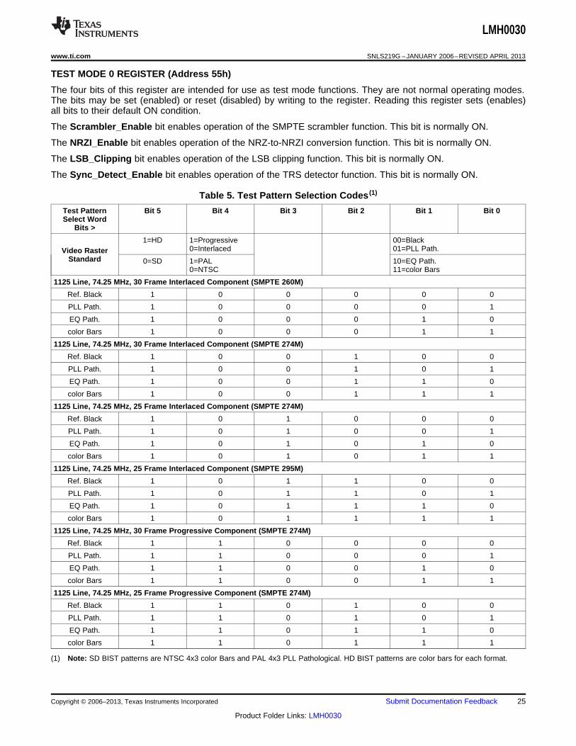
Table 5. Test Pattern Selection Codes (1)
Test Pattern Bit 5 Bit 4 Bit 3 Bit 2 Bit 1 Bit 0Select Word
Bits >
1=HD 1=Progressive 00=Black0=Interlaced 01=PLL Path.Video Raster
Standard 0=SD 1=PAL 10=EQ Path.0=NTSC 11=color Bars
1125 Line, 74.25 MHz, 30 Frame Interlaced Component (SMPTE 260M)
Ref. Black 1 0 0 0 0 0
PLL Path. 1 0 0 0 0 1
EQ Path. 1 0 0 0 1 0
color Bars 1 0 0 0 1 1
1125 Line, 74.25 MHz, 30 Frame Interlaced Component (SMPTE 274M)
Ref. Black 1 0 0 1 0 0
PLL Path. 1 0 0 1 0 1
EQ Path. 1 0 0 1 1 0
color Bars 1 0 0 1 1 1
1125 Line, 74.25 MHz, 25 Frame Interlaced Component (SMPTE 274M)
Ref. Black 1 0 1 0 0 0
PLL Path. 1 0 1 0 0 1
EQ Path. 1 0 1 0 1 0
color Bars 1 0 1 0 1 1
1125 Line, 74.25 MHz, 25 Frame Interlaced Component (SMPTE 295M)
Ref. Black 1 0 1 1 0 0
PLL Path. 1 0 1 1 0 1
EQ Path. 1 0 1 1 1 0
color Bars 1 0 1 1 1 1
1125 Line, 74.25 MHz, 30 Frame Progressive Component (SMPTE 274M)
Ref. Black 1 1 0 0 0 0
PLL Path. 1 1 0 0 0 1
EQ Path. 1 1 0 0 1 0
color Bars 1 1 0 0 1 1
1125 Line, 74.25 MHz, 25 Frame Progressive Component (SMPTE 274M)
Ref. Black 1 1 0 1 0 0
PLL Path. 1 1 0 1 0 1
EQ Path. 1 1 0 1 1 0
color Bars 1 1 0 1 1 1
(1) Note: SD BIST patterns are NTSC 4x3 color Bars and PAL 4x3 PLL Pathological. HD BIST patterns are color bars for each format.
Copyright © 2006–2013, Texas Instruments Incorporated Submit Documentation Feedback 25
Product Folder Links: LMH0030

LMH0030
SNLS219G –JANUARY 2006–REVISED APRIL 2013 www.ti.com
Table 5. Test Pattern Selection Codes(1) (continued)
Test Pattern Bit 5 Bit 4 Bit 3 Bit 2 Bit 1 Bit 0Select Word
Bits >
1125 Line, 74.25 MHz, 24 Frame Progressive Component (SMPTE 274M)
Ref. Black 1 1 1 0 0 0
PLL Path. 1 1 1 0 0 1
EQ Path. 1 1 1 0 1 0
color Bars 1 1 1 0 1 1
750 Line, 74.25 MHz, 60 Frame Progressive Component (SMPTE 296M)
Ref. Black 1 1 1 1 0 0
PLL Path. 1 1 1 1 0 1
EQ Path. 1 1 1 1 1 0
color Bars 1 1 1 1 1 1
525 Line, 30 Frame, 27 MHz, NTSC 4x3 (SMPTE 125M)
Ref. Black 0 0 0 0 0 0
PLL Path. 0 0 0 0 0 1
EQ Path. 0 0 0 0 1 0
color Bars (SD 0 0 0 0 1 1BIST)
625 Line, 25 Frame, 27 MHz, PAL 4x3 (ITU-T BT.601)
Ref. Black 0 1 0 0 0 0
PLL Path. (SD 0 1 0 0 0 1BIST)
EQ Path. 0 1 0 0 1 0
color Bars 0 1 0 0 1 1
525 Line, 30 Frame, 36 MHz, NTSC 16x9 (SMPTE 125M)
Ref. Black 0 0 0 1 0 0
PLL Path. 0 0 0 1 0 1
EQ Path. 0 0 0 1 1 0
color Bars 0 0 0 1 1 1
625 Line, 25 Frame, 36 MHz, PAL 16x9 (ITU-T BT.601)
Ref. Black 0 1 0 1 0 0
PLL Path. 0 1 0 1 0 1
EQ Path. 0 1 0 1 1 0
color Bars 0 1 0 1 1 1
525 Line, 30 Frame, 54 MHz (NTSC)
Ref. Black 0 0 1 0 0 0
PLL Path. 0 0 1 0 0 1
EQ Path. 0 0 1 0 1 0
color Bars 0 0 1 0 1 1
625 Line, 25 Frame, 54 MHz (PAL)
Ref. Black 0 1 1 0 0 0
PLL Path. 0 1 1 0 0 1
EQ Path. 0 1 1 0 1 0
color Bars 0 1 1 0 1 1
26 Submit Documentation Feedback Copyright © 2006–2013, Texas Instruments Incorporated
Product Folder Links: LMH0030

LMH0030
www.ti.com SNLS219G –JANUARY 2006–REVISED APRIL 2013
Table 6. I/O Configuration Register Addresses for Control Register Functions
Bit Address Pin # SEL [n] Power-OnRegister Bit I/P or O/P Status[5] [4] [3] [2] [1] [0]
reserved 0 0 0 0 0 0
FF Flag Error 0 0 0 0 0 1 Output
AP Flag Error 0 0 0 0 1 0 Output
ANC Flag 0 0 0 0 1 1 OutputError
CRC Error 0 0 0 1 0 0 Output I/O Port Bit 5(SD/HD)
Addresses x05h through x0Ch are reserved.
SAV 0 0 1 1 0 1 Output
EAV 0 0 1 1 1 0 Output
NSP 0 0 1 1 1 1 Output
F 0 1 0 0 1 0 Output I/O Port Bit 0
V 0 1 0 0 1 1 Output I/O Port Bit 1
H 0 1 0 1 0 0 Output I/O Port Bit 2
Format[0] 0 1 0 1 0 1 Output
Format[1] 0 1 0 1 1 0 Output
Format[2] 0 1 0 1 1 1 Output
Format[3] 0 1 1 0 0 0 Output
Format[4] 0 1 1 0 0 1 Output I/O Port Bit 3(SD/HD)
FIFO Full 0 1 1 0 1 0 Output
FIFO Empty 0 1 1 0 1 1 Output
Lock Detect 0 1 1 1 0 0 Output I/O Port Bit 4
Pass/Fail 0 1 1 1 0 1 Output I/O Port Bit 6
FIFO Overrun 0 1 1 1 1 0 Output
ANC Chksum 0 1 1 1 1 1 OutputError
EDH Force 1 0 0 0 0 0 Input
Test Pattern 1 0 0 0 0 1 InputSelect[0]
Test Pattern 1 0 0 0 1 0 InputSelect[1]
Test Pattern 1 0 0 0 1 1 InputSelect[2]
Test Pattern 1 0 0 1 0 0 InputSelect[3]
Test Pattern 1 0 0 1 0 1 InputSelect[4]
Test Pattern 1 0 0 1 1 0 InputSelect[5]
EDH Enable 1 0 0 1 1 1 Input
TPG Enable 1 0 1 0 0 0 Input I/O Port Bit 7
reserved 1 0 1 0 0 1
Chksum 1 0 1 0 1 0 InputAttach In
reserved 1 0 1 0 1 1
VPG Filter 1 0 1 1 0 0 InputEnable
Dither Enable 1 0 1 1 0 1 Input
Copyright © 2006–2013, Texas Instruments Incorporated Submit Documentation Feedback 27
Product Folder Links: LMH0030

LMH0030
SNLS219G –JANUARY 2006–REVISED APRIL 2013 www.ti.com
Table 6. I/O Configuration Register Addresses for Control Register Functions (continued)
Bit Address Pin # SEL [n] Power-OnRegister Bit I/P or O/P Status[5] [4] [3] [2] [1] [0]
FIFO Insert 1 0 1 1 1 1 InputEnable
28 Submit Documentation Feedback Copyright © 2006–2013, Texas Instruments Incorporated
Product Folder Links: LMH0030

LMH0030
www.ti.com SNLS219G –JANUARY 2006–REVISED APRIL 2013
PIN DESCRIPTIONS (1)
Pin Name Description
1 VDDPLLD Positive Power Supply Input (2.5V supply, PLL Logic)
2 VSSPLLD Negative Power Supply Input (2.5V supply, PLL Logic)
3 IO0 Multi-Function I/O Port
4 IO1 Multi-Function I/O Port
5 DV0 Parallel Video Input (HD=Chroma, SD=Luma & Chroma)
6 DV1 Parallel Video Input (HD=Chroma, SD=Luma & Chroma)
7 DV2 Parallel Video Input (HD=Chroma, SD=Luma & Chroma)
8 DV3 Parallel Video Input (HD=Chroma, SD=Luma & Chroma)
9 DV4 Parallel Video Input (HD=Chroma, SD=Luma & Chroma)
10 VSSD Negative Power Supply Input (2.5V supply, Digital Logic)
11 DV5 Parallel Video Input (HD=Chroma, SD=Luma & Chroma)
12 DV6 Parallel Video Input (HD=Chroma, SD=Luma & Chroma)
13 DV7 Parallel Video Input (HD=Chroma, SD=Luma & Chroma)
14 DV8 Parallel Video Input (HD=Chroma, SD=Luma & Chroma)
15 DV9 Parallel Video Input (HD=Chroma, SD=Luma & Chroma)
16 VDDD Positive Power Supply Input (2.5V supply, Digital Logic)
17 VSSD Negative Power Supply Input (2.5V supply, Digital Logic)
18 DV10 Parallel Video Input (HD=Luma)
19 DV11 Parallel Video Input (HD=Luma)
20 DV12 Parallel Video Input (HD=Luma)
21 DV13 Parallel Video Input (HD=Luma)
22 DV14 Parallel Video Input (HD=Luma)
23 VDDIO Positive Power Supply Input (3.3V supply, I/O)
24 DV15 Parallel Video Input (HD=Luma)
25 DV16 Parallel Video Input (HD=Luma)
26 DV17 Parallel Video Input (HD=Luma)
27 DV18 Parallel Video Input (HD=Luma)
28 DV19 Parallel Video Input (HD=Luma)
29 VSSIO Negative Power Supply Input (3.3V supply, I/O)
30 IO2 Multi-Function I/O Port
31 IO3 Multi-Function I/O Port
32 IO4 Multi-Function I/O Port
33 IO5 Multi-Function I/O Port
34 IO6 Multi-Function I/O Port
35 IO7 Multi-Function I/O Port
36 ACLK Ancillary/Control Clock Input
37 VDDD Positive Power Supply Input (2.5V supply, Digital Logic)
38 AD0 Ancillary/Control Data I/O Port
39 AD1 Ancillary/Control Data I/O Port
40 AD2 Ancillary/Control Data I/O Port
41 AD3 Ancillary/Control Data I/O Port
42 AD4 Ancillary/Control Data I/O Port
43 VSSD Negative Power Supply Input (2.5V supply, Digital Logic)
44 AD5 Ancillary/Control Data I/O Port
45 AD6 Ancillary/Control Data I/O Port
46 AD7 Ancillary/Control Data I/O Port
(1) Note: All LVCMOS inputs except VCLK and ACLK have internal pull-down devices.
Copyright © 2006–2013, Texas Instruments Incorporated Submit Documentation Feedback 29
Product Folder Links: LMH0030

LMH0030
SNLS219G –JANUARY 2006–REVISED APRIL 2013 www.ti.com
PIN DESCRIPTIONS(1) (continued)
Pin Name Description
47 AD8 Ancillary/Control Data I/O Port
48 AD9 Ancillary/Control Data I/O Port
49 RD/WR Ancillary/Control Data Port Read/Write Control Input
50 ANC/CTRL Ancillary/Control Data Port Function Control Input
51 VDDSD Positive Power Supply Input (3.3V supply, Output Driver)
52 RREFPRE Output Preemphasis Reference Resistor (4.75 KΩ, 1% Nom.)
53 RREFLVL Output Level Reference Resistor (4.75 KΩ, 1% Nom.)
54 VSSSD Negative Power Supply Input (3.3V supply, Output Driver)
55 VSSSD Negative Power Supply Input (3.3V supply, Output Driver)
56 SDO Serial Data True Output
57 VDDLS Positive Power Supply Input (3.3V supply, Level Shift)
58 SDO Serial Data Complement Output
59 VSSLS Negative Power Supply Input (3.3V supply, Level Shift)
60 VDDZ Positive Power Supply Input (2.5V supply, Serializer)
61 VSSPLLA Negative Power Supply Input (2.5V supply, PLL Analog)
62 VDDPLLA Positive Power Supply Input (2.5V supply, PLL Analog)
63 VCLK Video Data Clock Input
64 Reset Manual Reset Input (High True)
30 Submit Documentation Feedback Copyright © 2006–2013, Texas Instruments Incorporated
Product Folder Links: LMH0030

LMH0030
www.ti.com SNLS219G –JANUARY 2006–REVISED APRIL 2013
APPLICATION INFORMATION
Complete details for the SD130ASM evaluation PCB are available on TI’s WEB site. This circuit demonstratesthe capabilities of the LMH0030 and allows its evaluation in a native configuration. An assembled demonstrationboard kit, part number SD130EVK, complete with operating instructions, drawing package and list of materials isavailable. Contact the Interface Products Group or the Serial Digital Video and Interface Applications Group forordering information. Complete circuit board layouts, schematics and other information for the SD130EVK arealso available on TI's WEB site in the application information for this device. For latest product details andavailability information, please see: www.ti.com/appinfo/interface.
PCB LAYOUT AND POWER SYSTEM BYPASS RECOMMENDATIONS
Circuit board layout and stack-up for the LMH0030 should be designed to provide noise-free power to the device.Good layout practice also will separate high frequency or high level inputs and outputs to minimize unwantedstray noise pickup, feedback and interference. Power system performance may be greatly improved by using thindielectrics (4 to 10 mils) for power/ground sandwiches. This increases the intrinsic capacitance of the PCB powersystem which improves power supply filtering, especially at high frequencies, and makes the value andplacement of external bypass capacitors less critical. External bypass capacitors should include both RF ceramicand tantalum electrolytic types. RF capacitors may use values in the range 0.01 µF to 0.1 µF. Tantalumcapacitors may be in the range 2.2 µF to 10 µF. Voltage rating for tantalum capacitors should be at least 5X thepower supply voltage being used. It is recommended practice to use two vias at each power pin of the LMH0030as well as all RF bypass capacitor terminals. Dual vias reduce the interconnect inductance by up to half, therebyreducing interconnect inductance and extending the effective frequency range of the bypass components.
The outer layers of the PCB may be flooded with additional VSS (ground) plane. These planes will improveshielding and isolation as well as increase the intrinsic capacitance of the power supply plane system. Naturally,to be effective, these planes must be tied to the VSS power supply plane at frequent intervals with vias. Frequentvia placement also improves signal integrity on signal transmission lines by providing short paths for imagecurrents which reduces signal distortion. The planes should be pulled back from all transmission lines andcomponent mounting pads a distance equal to the width of the widest transmission line or the thickness of thedielectric separating the transmission line from the internal power or ground plane(s) whichever is greater. Doingso minimizes effects on transmission line impedances and reduces unwanted parasitic capacitances atcomponent mounting pads.
The LMH0030 uses two power supply voltages, 2.5 and 3.3 volts. These supplies connect to the device throughseven sets of independent power input pins. The function and system supplied through these is given in the PinDescription Table. The power supply voltages normally share a common 0 volt or ground return system. Either asplit plane or separate power planes can be used to supply the positive voltages to the device.
In especially noisy power supply environments, such as is often the case when using switching power supplies,separate filtering may be used at the LMH0030's PLL analog, PLL digital and serial output driver power pins. TheLMH0030 was designed for this situation. The digital section, PLL and output driver power supply feeds areindependent. See the Pin Description Table and the Connection Diagram for details. Supply filtering may take theform of L-section or pi-section, L-C filters in series with these VDD inputs. Such filters are available in a singlepackage from several manufacturers. Despite being independent feeds, all device power supplies should beapplied simultaneously as from a common source.
Copyright © 2006–2013, Texas Instruments Incorporated Submit Documentation Feedback 31
Product Folder Links: LMH0030

LMH0030
SNLS219G –JANUARY 2006–REVISED APRIL 2013 www.ti.com
PROCESSING NON-SUPPORTED AND pSf RASTER FORMATS
The number and type of HD raster formats has proliferated greatly since the LMH0030 was designed. Thoughnot specifically capable of fully or automatically processing these new formats, the LMH0030 may still be capableof serializing them. The user is encouraged to experiment with processing of these formats keeping in mind thatthe LMH0030 has not been tested to handle raster formats other than those detailed in Table 4. Therefore, theresults from attempts to process non-supported formats is not ensured. The following guidelines concerningdevice setup are provided to aid the user in configuring the LMH0030 to attempt limited processing of these otherraster formats. In general, the device is configured to defeat its format and TRS detection function and to limitoperation to a generic HD format type. (The user should consult Table 4 for guidance on the format groupssimilar to the non-supported one to be processed). Since these newer formats are in the HD realm, the LMH0030should be configured to operate in HD-ONLY mode by setting bit-5 of the FORMAT 0 register (address 0Bh).Also, the device should be further configured by loading the FORMAT SET[4:0] bits of this register with a non-specific HD sub-format code. The complete data word for this HD sub-format code with HD-ONLY bit set is 33Fh(all 10 bits of AD[9:0]). Since this format differs from those in the table, the EAV/SAV indicators are disabled.Without these indicators, line numbering and CRC insertion are disabled and ancillary data insertion will notfunction. Pre-processing of the parallel data ahead of the LMH0030 will be required to insert CRC data and linenumbering.
Among the specialized formats are so-called progressive-segmented frame formats (pSf). Refer to SMPTE274M-2003, Annex A. These formats are composed of the video lines of progressive scan rasters rearranged inthe manner of an interlaced raster. The even numbered lines are arranged to form Field 1 and the odd numberedlines form Field 2. In other respects, the format is identical to the normal interlaced format. The LMH0030 canserialize these pSf formats provided that the lines of the original progressive raster are first rearranged externallyto the LMH0030 before being presented to it for processing.
32 Submit Documentation Feedback Copyright © 2006–2013, Texas Instruments Incorporated
Product Folder Links: LMH0030
LMH0030
www.ti.com SNLS219G –JANUARY 2006–REVISED APRIL 2013
REVISION HISTORY
Changes from Revision F (April 2013) to Revision G Page
• Changed layout of National Data Sheet to TI format .......................................................................................................... 32
Copyright © 2006–2013, Texas Instruments Incorporated Submit Documentation Feedback 33
Product Folder Links: LMH0030
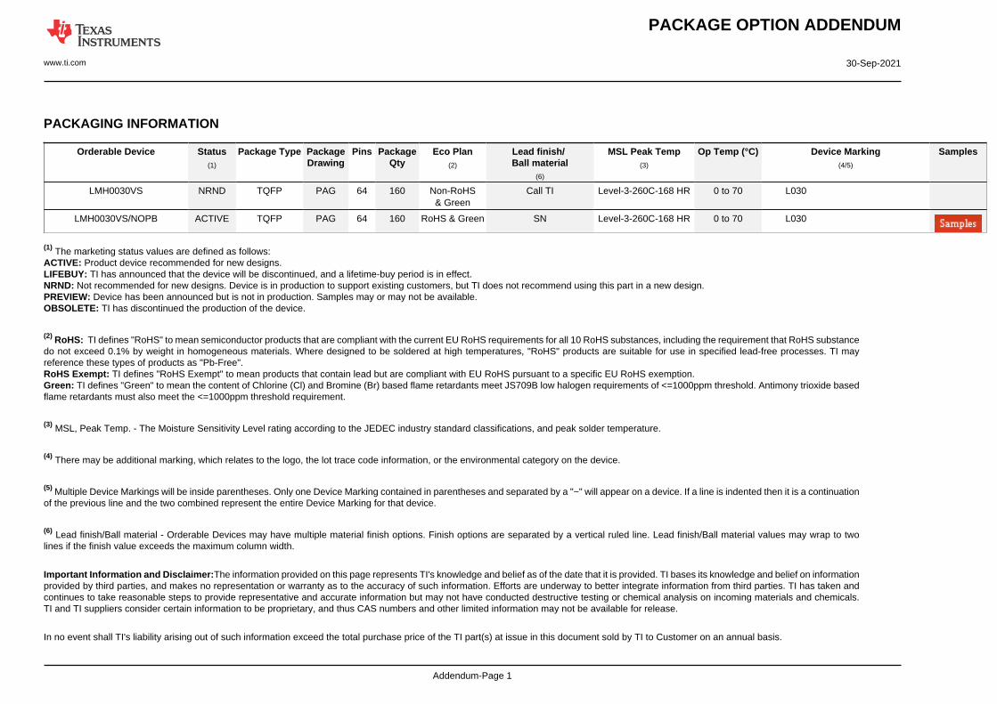
PACKAGE OPTION ADDENDUM
www.ti.com 30-Sep-2021
Addendum-Page 1
PACKAGING INFORMATION
Orderable Device Status(1)
Package Type PackageDrawing
Pins PackageQty
Eco Plan(2)
Lead finish/Ball material
(6)
MSL Peak Temp(3)
Op Temp (°C) Device Marking(4/5)
Samples
LMH0030VS NRND TQFP PAG 64 160 Non-RoHS& Green
Call TI Level-3-260C-168 HR 0 to 70 L030
LMH0030VS/NOPB ACTIVE TQFP PAG 64 160 RoHS & Green SN Level-3-260C-168 HR 0 to 70 L030
(1) The marketing status values are defined as follows:ACTIVE: Product device recommended for new designs.LIFEBUY: TI has announced that the device will be discontinued, and a lifetime-buy period is in effect.NRND: Not recommended for new designs. Device is in production to support existing customers, but TI does not recommend using this part in a new design.PREVIEW: Device has been announced but is not in production. Samples may or may not be available.OBSOLETE: TI has discontinued the production of the device.
(2) RoHS: TI defines "RoHS" to mean semiconductor products that are compliant with the current EU RoHS requirements for all 10 RoHS substances, including the requirement that RoHS substancedo not exceed 0.1% by weight in homogeneous materials. Where designed to be soldered at high temperatures, "RoHS" products are suitable for use in specified lead-free processes. TI mayreference these types of products as "Pb-Free".RoHS Exempt: TI defines "RoHS Exempt" to mean products that contain lead but are compliant with EU RoHS pursuant to a specific EU RoHS exemption.Green: TI defines "Green" to mean the content of Chlorine (Cl) and Bromine (Br) based flame retardants meet JS709B low halogen requirements of <=1000ppm threshold. Antimony trioxide basedflame retardants must also meet the <=1000ppm threshold requirement.
(3) MSL, Peak Temp. - The Moisture Sensitivity Level rating according to the JEDEC industry standard classifications, and peak solder temperature.
(4) There may be additional marking, which relates to the logo, the lot trace code information, or the environmental category on the device.
(5) Multiple Device Markings will be inside parentheses. Only one Device Marking contained in parentheses and separated by a "~" will appear on a device. If a line is indented then it is a continuationof the previous line and the two combined represent the entire Device Marking for that device.
(6) Lead finish/Ball material - Orderable Devices may have multiple material finish options. Finish options are separated by a vertical ruled line. Lead finish/Ball material values may wrap to twolines if the finish value exceeds the maximum column width.
Important Information and Disclaimer:The information provided on this page represents TI's knowledge and belief as of the date that it is provided. TI bases its knowledge and belief on informationprovided by third parties, and makes no representation or warranty as to the accuracy of such information. Efforts are underway to better integrate information from third parties. TI has taken andcontinues to take reasonable steps to provide representative and accurate information but may not have conducted destructive testing or chemical analysis on incoming materials and chemicals.TI and TI suppliers consider certain information to be proprietary, and thus CAS numbers and other limited information may not be available for release.
In no event shall TI's liability arising out of such information exceed the total purchase price of the TI part(s) at issue in this document sold by TI to Customer on an annual basis.

PACKAGE OPTION ADDENDUM
www.ti.com 30-Sep-2021
Addendum-Page 2

MECHANICAL DATA
MTQF006A – JANUARY 1995 – REVISED DECEMBER 1996
POST OFFICE BOX 655303 • DALLAS, TEXAS 75265
PAG (S-PQFP-G64) PLASTIC QUAD FLATPACK
0,13 NOM
0,25
0,450,75
Seating Plane
0,05 MIN
4040282/C 11/96
Gage Plane
33
0,170,27
16
48
1
7,50 TYP
49
64
SQ
9,80
1,050,95
11,8012,20
1,20 MAX
10,20SQ
17
32
0,08
0,50 M0,08
0°–7°
NOTES: A. All linear dimensions are in millimeters.B. This drawing is subject to change without notice.C. Falls within JEDEC MS-026

IMPORTANT NOTICE AND DISCLAIMERTI PROVIDES TECHNICAL AND RELIABILITY DATA (INCLUDING DATASHEETS), DESIGN RESOURCES (INCLUDING REFERENCEDESIGNS), APPLICATION OR OTHER DESIGN ADVICE, WEB TOOLS, SAFETY INFORMATION, AND OTHER RESOURCES “AS IS”AND WITH ALL FAULTS, AND DISCLAIMS ALL WARRANTIES, EXPRESS AND IMPLIED, INCLUDING WITHOUT LIMITATION ANYIMPLIED WARRANTIES OF MERCHANTABILITY, FITNESS FOR A PARTICULAR PURPOSE OR NON-INFRINGEMENT OF THIRDPARTY INTELLECTUAL PROPERTY RIGHTS.These resources are intended for skilled developers designing with TI products. You are solely responsible for (1) selecting the appropriateTI products for your application, (2) designing, validating and testing your application, and (3) ensuring your application meets applicablestandards, and any other safety, security, or other requirements. These resources are subject to change without notice. TI grants youpermission to use these resources only for development of an application that uses the TI products described in the resource. Otherreproduction and display of these resources is prohibited. No license is granted to any other TI intellectual property right or to any third partyintellectual property right. TI disclaims responsibility for, and you will fully indemnify TI and its representatives against, any claims, damages,costs, losses, and liabilities arising out of your use of these resources.TI’s products are provided subject to TI’s Terms of Sale (https:www.ti.com/legal/termsofsale.html) or other applicable terms available eitheron ti.com or provided in conjunction with such TI products. TI’s provision of these resources does not expand or otherwise alter TI’sapplicable warranties or warranty disclaimers for TI products.IMPORTANT NOTICE
Mailing Address: Texas Instruments, Post Office Box 655303, Dallas, Texas 75265Copyright © 2021, Texas Instruments Incorporated