Embed Size (px)
Citation preview
Sh-Semi12-01E
Headquarters:Senju Hashido-cho 23, Adachi-ku, Tokyo 120-8555, Japan Phone:(81)3-3888-5151, Fax:(81)3-3870-3032 www.senju-m.co.jp
Sh-Semi12-01E
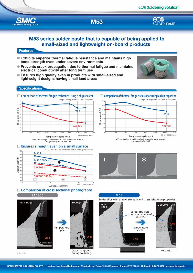
M53
□ Ensures strength even on a small surface
Surface area (mm2)
□ Comparison of thermal fatigue resistance using a chip capacitorShear strength (N)
□ Comparison of cross sectional photographs
3000cyc
Chip
ChipChip
3000cyc
Chip
□ Comparison of thermal fatigue resistance using a chip resistor Using a 3216 chip resistor and a large-sized pattern Using a 3216 chip resistor and a medium-sized pattern
Using a 3216 chip resistor and small-, medium- and large-sized patterns
M53 series solder paste that is capable of being applied tosmall-sized and lightweight on-board products
●
●
●
Features
Exhibits superior thermal fatigue resistance and maintains high bond strength even under severe environmentsPrevents crack propagation due to thermal fatigue and maintains electrical conductivity after long term useEnsures high quality even in products with small-sized and lightweight designs having small land areas
Shear strength (N)
□ Comparison of thermal fatigue resistance using a chip capacitor□ Comparison of thermal fatigue resistance using a chip resistorUsing a 3216 chip resistor and a large-sized pattern Using a 3216 chip resistor and a medium-sized pattern
● Ensures high quality even in products with small-sized and lightweight designs having small land areas
Specifications
Larger structurecompared to that of
SAC305
Shear strength (N)
Temperature cycle (cyc.)M53 containing Bi and In exhibits a much lower decrease in
strength compared to SAC305
90
80
70
60
50
40
30
20
10
0
M53M53M53
TCT;-40/+124℃(30min)
450040003500300025002000150010005000
SAC305SAC305SAC305
Temperature cycle (cyc.)M53 containing Bi and In maintains superior shear strength
compared to SAC305
TCT;-40/+124℃(30min)
3500300025002000150010005000
70.0
60.0
50.0
40.0
30.0
20.0
10.0
0
M53M53M53
SAC305SAC305SAC305
1
L M S
TCT;-40/+125℃(30min)15225335
90.0
80.0
70.0
60.0
50.0
40.0
30.0
20.0
10.0
0.0
M53 InM53 InM53 In
M53 3000cyc.M53 3000cyc.M53 3000cyc.
SAC305 3000cyc.SAC305 3000cyc.
SAC305 InSAC305 InSAC305 In
SAC305 3000cyc.SAC305 3000cyc.SAC305 3000cyc.
SAC305 M53
Initial stage
Temperaturecycle
Crack has grownduring soldering
Solder alloy with greater strength and stress relaxation properties
Temperaturecycle
No cracks
Initialstage
Sh-Semi12-02E
Headquarters:Senju Hashido-cho 23, Adachi-ku, Tokyo 120-8555, Japan Phone:(81)3-3888-5151, Fax:(81)3-3870-3032 www.senju-m.co.jp
Sh-Semi12-02E
●
●
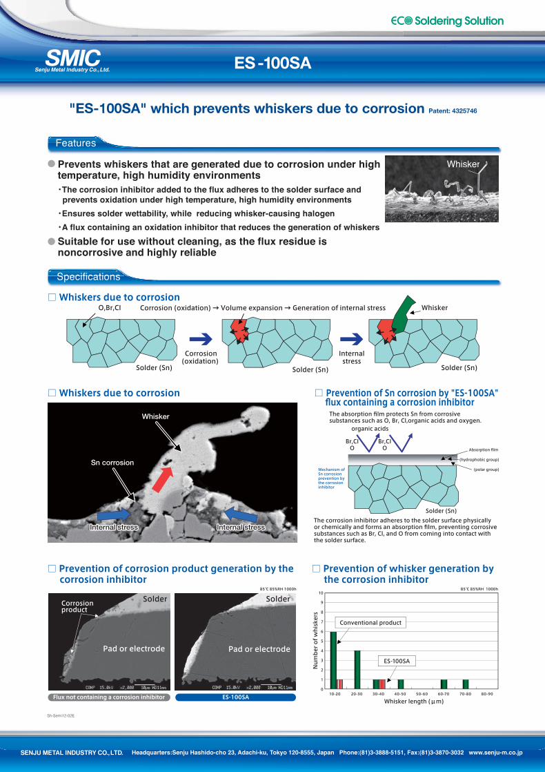
"ES-100SA" which prevents whiskers due to corrosion Patent: 4325746
ES-100SA
●
Specifications
Whisker
□ Prevention of Sn corrosion by "ES-100SA" flux containing a corrosion inhibitor
□ Prevention of corrosion product generation by the corrosion inhibitor
□ Prevention of whisker generation by the corrosion inhibitor
85℃ 85%RH 1000h
The absorption film protects Sn from corrosivesubstances such as O, Br, Cl,organic acids and oxygen.
Solder (Sn)
Br,CIO
O,Br,CI□ Whiskers due to corrosion
Corrosion (oxidation) → Volume expansion → Generation of internal stress Whisker
Solder (Sn) Solder (Sn) Solder (Sn)
Internalstress
Corrosion(oxidation)
85℃ 85%RH 1000h
Number of whiskers
Conventional product
10
9
8
7
6
5
4
3
2
1
010-20 20-30 30-40 50-6040-50 60-70 70-80 80-90
ES-100SA
Whisker
Sn corrosion
□ Whiskers due to corrosion
Whisker length (μm)
Prevents whiskers that are generated due to corrosion under high temperature, high humidity environments ・The corrosion inhibitor added to the flux adheres to the solder surface and prevents oxidation under high temperature, high humidity environments
・Ensures solder wettability, while reducing whisker-causing halogen
・A flux containing an oxidation inhibitor that reduces the generation of whiskers
Suitable for use without cleaning, as the flux residue is noncorrosive and highly reliable
●
ES 100SA which prevents whiskers due to corrosion"ES-100SA" which prevents whiskers due to corrosion Patent: 4325746Patent: 4325746
WhiskerPrevents whiskers that are generated due to corrosion under high temperature, high humidity environments
Features
Br,CIO
Internal stressInternal stressInternal stress Internal stressInternal stressInternal stress
organic acids
The corrosion inhibitor adheres to the solder surface physically or chemically and forms an absorption film, preventing corrosive substances such as Br, Cl, and O from coming into contact with the solder surface.
Absorption film
(hydrophobic group)
(polar group) Mechanism of Sn corrosionprevention by the corrosioninhibitor
Solder
Pad or electrode
Solder
Pad or electrode
Corrosionproduct
Flux not containing a corrosion inhibitor ES-100SA
Sh-Semi12-03E
Sh-Semi12-03E
Headquarters:Senju Hashido-cho 23, Adachi-ku, Tokyo 120-8555, Japan Phone:(81)3-3888-5151, Fax:(81)3-3870-3032 www.senju-m.co.jp
Solution for problems in power device packaging
Uniform thickness Reduction of voids High-quality alloy
□ Schematic diagram of a power module
HQ
□ Good joints and a reduction of voids were realized by developing Ni balls and a sheet-forming technique
□ Good solder wettability is maintained by preventing surface oxidation through sheet formation using a unique technique.
Crack dueto incline
Solder
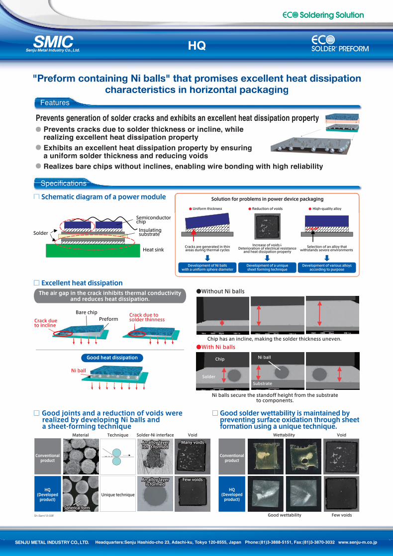
"Preform containing Ni balls" that promises excellent heat dissipationcharacteristics in horizontal packaging
●
●
● Prevents cracks due to solder thickness or incline, whilerealizing excellent heat dissipation propertyExhibits an excellent heat dissipation property by ensuringa uniform solder thickness and reducing voids Realizes bare chips without inclines, enabling wire bonding with high reliability
Preform containing Ni balls that promises excellent heat dissipation"Preform containing Ni balls" that promises excellent heat dissipationcharacteristics in horizontal packagingcharacteristics in horizontal packagingh i i i h i l k i
● Prevents cracks due to solder thickness or incline, while
Features
Solder-Ni interface
Unique technique
Void
Prevents generation of solder cracks and exhibits an excellent heat dissipation property
Solution for problems in power device packaging
Uniform thickness Reduction of voids High-quality alloy
□Schematic diagram of a power module
●a uniform solder thickness and reducing voids Realizes bare chips without inclines, enabling wire bonding with high reliability
Specifications
Solder
Semiconductorchip
Insulatingsubstrate
Heat sink
Development of Ni ballswith a uniform sphere diameter
Development of a uniquesheet forming technique
Development of various alloysaccording to purpose
Cracks are generated in thinareas during thermal cycles
Increase of voids↓Deterioration of electrical resistanceand heat dissipation property
Selection of an alloy thatwithstands severe environments
□ Excellent heat dissipation
Chip has an incline, making the solder thickness uneven.
Ni balls secure the standoff height from the substrateto components.
●Without Ni balls
●With Ni balls
Ni ball
Substrate
Chip
Conventionalproduct
HQ(Developedproduct)
Wettability Void
Good wettability Few voids
Material
Conventionalproduct
HQ(Developedproduct)
An alloy layerAn alloy layerisnisn’t formedt formed
An alloy layerAn alloy layeris formedis formed
An alloy layerisn’t formed
An alloy layeris formed
Many voidsMany voids
Few voidsFew voids
Many voids
Few voids
Spherical formSpherical formSpherical form
The air gap in the crack inhibits thermal conductivityand reduces heat dissipation.
Crack due tosolder thinnessPreform
Bare chip
Good heat dissipation
Ni ball
Technique
Sh-Semi12-04E
Sh-Semi12-04E
Headquarters:Senju Hashido-cho 23, Adachi-ku, Tokyo 120-8555, Japan Phone:(81)3-3888-5151, Fax:(81)3-3870-3032 www.senju-m.co.jp
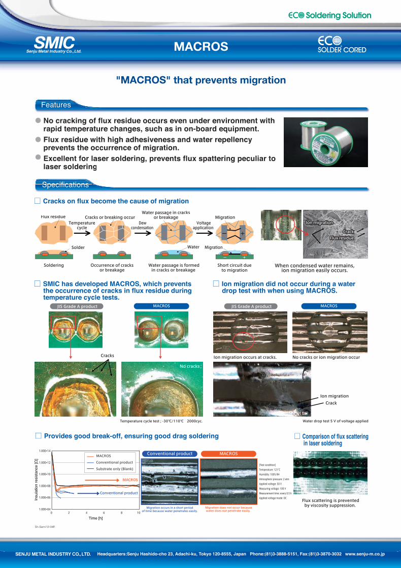
□ Cracks on flux become the cause of migration
Ion migration
Crack
Water passage in cracksor breakage
Migration
Migration
Short circuit dueto migration
Water passage is formedin cracks or breakage
Water
Voltageapplication
Dewcondensation
Flux residueTemperature
cycle
Cracks or breaking occur
Occurrence of cracksor breakage
Solder
Soldering
Features
●
●
● No cracking of flux residue occurs even under environment with rapid temperature changes, such as in on-board equipment.Flux residue with high adhesiveness and water repellency prevents the occurrence of migration.Excellent for laser soldering, prevents flux spattering peculiar to laser soldering
MACROS
"MACROS" that prevents migration
□ Cracks on flux become the cause of migration
Water passage in cracksFl id
● Excellent for laser soldering, prevents flux spattering peculiar to laser soldering
Specifications
Flux scattering is preventedby viscosity suppression.
Ion migrationIon migrationIon migration
CrackCrackCrackFlux residueFlux residueFlux residue
When condensed water remains,ion migration easily occurs.
1.00E+04
1.00E+06
1.00E+08
1.00E+10
1.00E+12
1.00E+14
0 2 4 6 8 10
MACROS
[Test condition]
Temperature: 121°C
Humidity: 100% RH
Atmospheric pressure: 2 atm
Applied voltage: 50 V
Measuring voltage: 100 V
Measurement time: every 0.5 h
Applied voltage mode: DC
MACROS
□ Comparison of flux scatteringin laser soldering
Insu
latio
n re
sist
ance
[Ω]
Time [h]
□ Provides good break-off, ensuring good drag soldering
MACROS
Conventional product
Substrate only (Blank)
Conventional product
Conventional product
Migration does not occur becausewater does not penetrate easily.
Migration occurs in a short periodof time because water penetrates easily.
MACROS MACROS
□ SMIC has developed MACROS, which prevents the occurrence of cracks in flux residue during temperature cycle tests.
JIS Grade A product
Temperature cycle test ; -30℃/110℃ 2000cyc.
No cracks
Cracks
Water drop test 5 V of voltage applied
JIS Grade A product
□ Ion migration did not occur during a water drop test with when using MACROS.
Ion migration occurs at cracks. No cracks or ion migration occur
Sh-Semi12-05E
Sh-Semi12-05E
Headquarters:Senju Hashido-cho 23, Adachi-ku, Tokyo 120-8555, Japan Phone:(81)3-3888-5151, Fax:(81)3-3870-3032 www.senju-m.co.jp
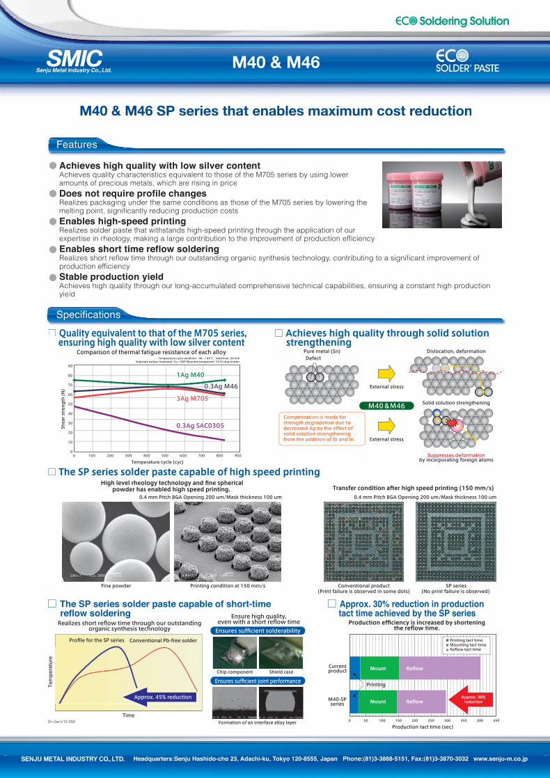
□ Quality equivalent to that of the M705 series, ensuring high quality with low silver content
□ Approx. 30% reduction in production tact time achieved by the SP series
Production efficiency is increased by shorteningthe reflow time.
M40 & M46
M40 & M46 SP series that enables maximum cost reduction
Achieves high quality with low silver contentAchieves quality characteristics equivalent to those of the M705 series by using lower amounts of precious metals, which are rising in price
Does not require profile changesRealizes packaging under the same conditions as those of the M705 series by lowering the melting point, significantly reducing production costs
Enables high-speed printingRealizes solder paste that withstands high-speed printing through the application of ourexpertise in rheology, making a large contribution to the improvement of production efficiency
Enables short time reflow solderingRealizes short reflow time through our outstanding organic synthesis technology, contributing to a significant improvement of production efficiency
Stable production yieldAchieves high quality through our long-accumulated comprehensive technical capabilities, ensuring a constant high production yield
●
●
●
●
●
M40 & M46 SP series that enables maximum cost reductionM40 & M46 SP series that enables maximum cost reduction
Achieves high quality with low silver contentAchieves quality characteristics equivalent to those of the M705 series by using loweramounts of precious metals, which are rising in price
●
Features
□Quality equivalent to that of the M705 series, ensuring high quality with low silver content
y qy q
Stable production yieldAchieves high quality through our long-accumulated comprehensive technical capabilities, ensuring a constant high productionyield
●
Specifications
External stress
External stress
M40&M46
90
80
70
60
50
40
30
20
10
00 100 200 300 400 500 600 700 800 900
1Ag M401Ag M401Ag M40
0.3Ag M460.3Ag M460.3Ag M46
3Ag M7053Ag M7053Ag M705
0.3Ag SAC03050.3Ag SAC03050.3Ag SAC0305
Temperature cycle condition: -40 - + 85°C Hold time: 30 minSubstrate surface treatment: Cu + OSP Mounted component: 3216 chip resistor
Temperature cycle (cyc)
Shear strength (N)
Comparison of thermal fatigue resistance of each alloy
□ Achieves high quality through solid solution strengthening
Compensation is made for strength degradation due to decreased Ag by the effect of solid solution strengthening from the addition of Bi and In.
Pure metal (Sn)Defect
Dislocation, deformation
Solid solution strengthening
Suppresses deformationby incorporating foreign atoms
Transfer condition after high speed printing (150 mm/s)
Ensure high quality,even with a short reflow time
Approx. 45% reduction
Conventional product(Print failure is observed in some dots)
SP series(No print failure is observed)
0.4 mm Pitch BGA Opening 200 um/Mask thickness 100 um
Fine powder Printing condition at 150 mm/s
0.4 mm Pitch BGA Opening 200 um/Mask thickness 100 um
High level rheology technology and fine sphericalpowder has enabled high speed printing.
□ The SP series solder paste capable of high speed printing
□ The SP series solder paste capable of short-time reflow solderingRealizes short reflow time through our outstanding
organic synthesis technology
Conventional Pb-free solderProfile for the SP series
Temperature
Time
Chip component Shield case
Ensures sufficient solderability
Ensures sufficient joint performance
Formation of an interface alloy layerProduction tact time (sec)
0 50 100 150 200 250 300 350 400 450
Currentproduct
M40-SPseries
Printing
Mount Reflow
Mount Reflow
Printing tact timeMounting tact time Reflow tact time
Approx. 30%reduction
Sh-Semi12-06E
Sh-Semi12-06E
Headquarters:Senju Hashido-cho 23, Adachi-ku, Tokyo 120-8555, Japan Phone:(81)3-3888-5151, Fax:(81)3-3870-3032 www.senju-m.co.jp
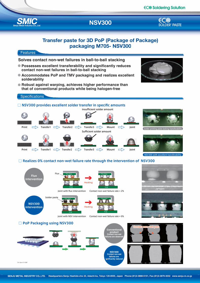
□ PoP Packaging using NSV300
NSV300
Transfer paste for 3D PoP (Package of Package)packaging M705- NSV300
●
●
●
Possesses excellent transferability and significantly reduces contact non-wet failures in ball-to-ball stackingAccommodates PoP and TMV packaging and realizes excellent solderabilityRobust against warping, achieves higher performance than that of conventional products while being halogen-free
Transfer paste for 3D PoP (Package of Package)Transfer paste for 3D PoP (Package of Package)packaging M705- NSV300packaging M705 NSV300
● Possesses excellent transferability and significantly reduces
Features
● Robust against warping, achieves higher performance than that of conventional products while being halogen-free
Specifications
Solves contact non-wet failures in ball-to-ball stacking
□ NSV300 provides excellent solder transfer in specific amounts
□ Realizes 0% contact non-wet failure rate through the intervention of NSV300
Solder paste
Flux
Heating
Heating
Joint with flux intervention Contact non-wet failure rate = 2%
Joint with NSV intervention Contact non-wet failure rate = 0%
Transfer1 Transfer2 Transfer3
Transfer1 Transfer2 Transfer3 Mount JointPrint
Mount JointPrint
Insufficient solder amount
Conventionalproduct
Contact non-wetfailures are observed
NSV300Contact non-wet
failures are ignificantly reduced
NSV300intervention
Fluxintervention
Solder printing paste lacking transferability
NSV300 with excellent transferability
Sufficient solder amount
Contact non-wet pastContact non-wet pastContact non-wet past
Sh-Semi12-07E
Sh-Semi12-07E
Headquarters:Senju Hashido-cho 23, Adachi-ku, Tokyo 120-8555, Japan Phone:(81)3-3888-5151, Fax:(81)3-3870-3032 www.senju-m.co.jp
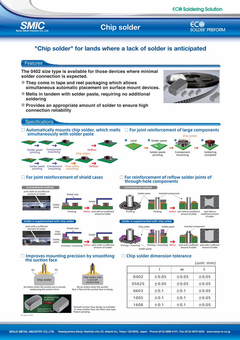
□ Automatically mounts chip solder, which melts simultaneously with solder paste
□ For reinforcement of reflow solder joints of through-hole components
□ For joint reinforcement of large components
Air enters when the suction ace is curved,weakening the suction force.
No air enters when the suctionface is flat and the suction face is strong.
Printing Joint with an insufficientamount of solder
Chip solder
"Chip solder" for lands where a lack of solder is anticipatedChip solder for lands where a lack of solder is anticipated"Chip solder" for lands where a lack of solder is anticipated
Features
●
●
●
They come in tape and reel packaging which allows simultaneous automatic placement on surface mount devices.Melts in tandem with solder paste, requiring no additional solderingProvides an appropriate amount of solder to ensure high connection reliability
□ Automatically mounts chip solder, which melts simultaneously with solder paste
y py □ For joint reinforcement of large components
● Provides an appropriate amount of solder to ensure high connection reliability
Specifications
y
Solder pasteprinting
Componentmounting
Reflow Chip solder
Chip soldermounting
Solder pasteprinting
Componentmounting
Reflow
Componentmounting
Land Solder paste
Solder pasteprinting
LargeLargecomponentcomponentLarge
component
Chip solder
Solderingcomplete
Solder is supplemented with chip solder Solder is supplemented with chip solder
□ For joint reinforcement of shield cases
l
±0.05
±0.05
±0.1
±0.1
±0.1
0402
05025
0603
1005
1608
±0.05
±0.05
±0.1
±0.1
±0.1
w
±0.05
±0.05
±0.05
±0.05
±0.05
t
□ Improves mounting precision by smoothing the suction face
Chip solder
Air Air
Chip solder witha smoothsuction face
Smoothing of thesuction face
Improvement ofmounting precision
* Smooth suction face design is available in sizes smaller than the 0603-size type* Patent pending
□ Chip solder dimension tolerance(unit: mm)
Conventional methodJoint with an insufficientamount of solder
Solder
Shield case
Solderpaste
Printing + mounting Joint with a sufficientamount of solder
SolderChipsolder
Shield caseJoint with a sufficientamount of solder
Conventional method
Solder paste Inserted component
Printing ReflowPrinting Joint with an insufficient amount of solder
Joint with aninsufficient amount
of solder
Chip solder Solder paste Inserted component
Printing + mountingSolder paste
Printing + mounting Reflow Joint with a sufficientamount of solder
Joint with a sufficientamount of solder
Reflow
Reflow
Solderpaste
The 0402 size type is available for those devices where minimal solder connection is expected.
Sh-Semi12-08E
Sh-Semi12-08E
Headquarters:Senju Hashido-cho 23, Adachi-ku, Tokyo 120-8555, Japan Phone:(81)3-3888-5151, Fax:(81)3-3870-3032 www.senju-m.co.jp
µ
µ
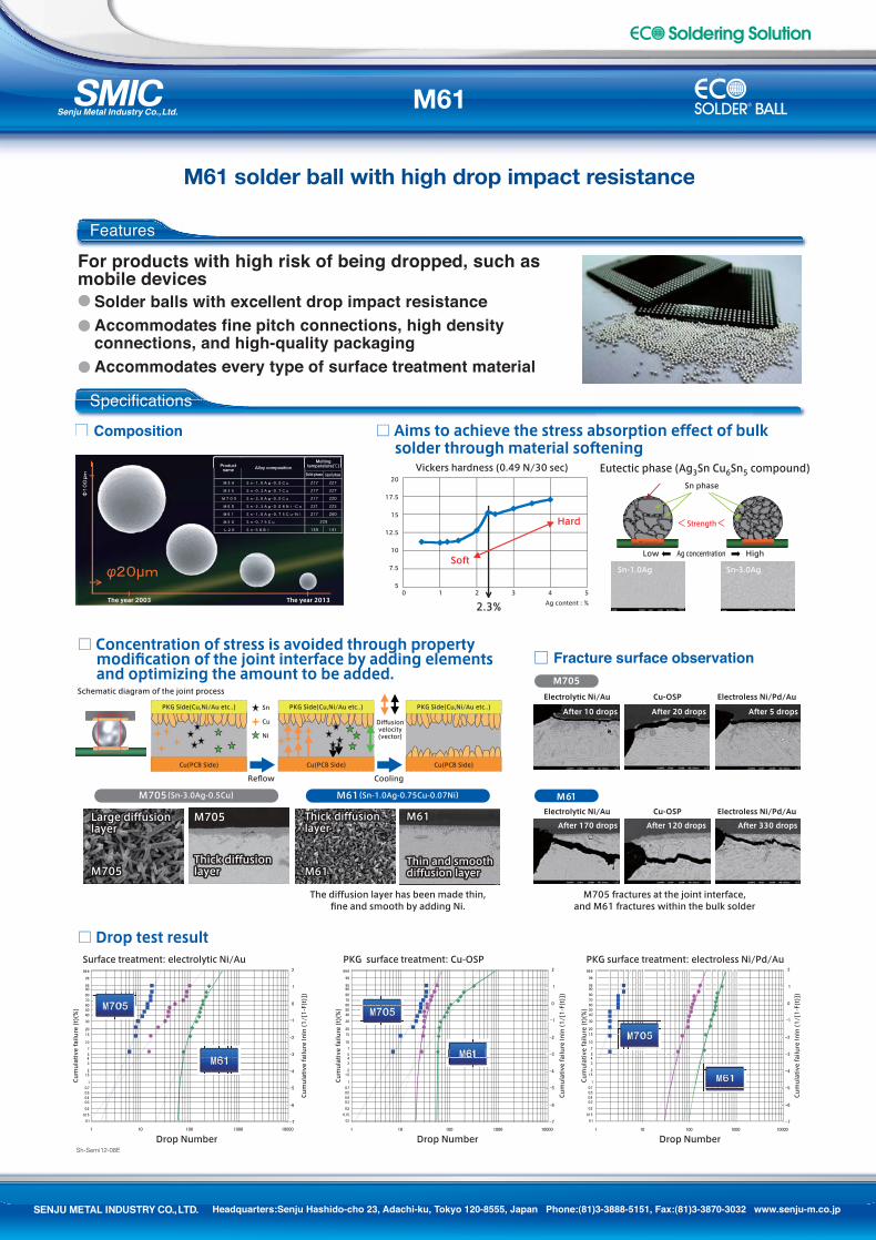
□ Composition
M61
M61 solder ball with high drop impact resistance
●
●
●
Solder balls with excellent drop impact resistance Accommodates fine pitch connections, high density connections, and high-quality packagingAccommodates every type of surface treatment material
M61 solder ball with high drop impact resistanceM61 solder ball with high drop impact resistance
● S ld b ll ith ll t d i t i t
Features
□ Composition
●connections, and high-quality packagingAccommodates every type of surface treatment material
Specifications
Productname Alloy composition
Meltingtemperature(℃)
Solid phase Liquid phase
For products with high risk of being dropped, such as mobile devices
The diffusion layer has been made thin,fine and smooth by adding Ni.
Cumulative failure InIn (1/[1-F(t)])
Ag content : %
Sn-3.0AgSn-1.0Ag
2.3%
□ Aims to achieve the stress absorption effect of bulk solder through material softening
Eutectic phase (Ag3Sn Cu6Sn5 compound)Vickers hardness (0.49 N/30 sec)
Hard
Soft
20
17.5
15
12.5
10
7.5
50 1 2 3 4 5
Sn phase
Strength
Ag concentrationLow High
M61
M705
□ Fracture surface observation
M705 fractures at the joint interface,and M61 fractures within the bulk solder
Drop NumberDrop Number Drop Number
Electrolytic Ni/Au Electroless Ni/Pd/AuCu-OSP
After 10 drops After 5 dropsAfter 20 drops
Electrolytic Ni/Au Electroless Ni/Pd/AuCu-OSP
After 170 drops After 330 dropsAfter 120 drops
M705(Sn-3.0Ag-0.5Cu) M61(Sn-1.0Ag-0.75Cu-0.07Ni)
Thick diffusionThick diffusionlayerlayerThick diffusionlayer
M61M61M61Thin and smoothThin and smoothdiffusion layerdiffusion layerThin and smoothdiffusion layer
M61M61M61
Thick diffusionThick diffusionlayerlayerThick diffusionlayer
M705
M705M705M705
Large diffusionLarge diffusionlayerlayerLarge diffusionlayer
□ Concentration of stress is avoided through property modification of the joint interface by adding elements and optimizing the amount to be added.
Reflow Cooling
Diffusionvelocity(vector)
Cu(PCB Side)
PKG Side(Cu,Ni/Au etc..) PKG Side(Cu,Ni/Au etc..)
Cu(PCB Side)
PKG Side(Cu,Ni/Au etc..)
Cu(PCB Side)
Sn
Cu
Ni
Schematic diagram of the joint process
□ Drop test resultSurface treatment: electrolytic Ni/Au PKG surface treatment: Cu-OSP PKG surface treatment: electroless Ni/Pd/Au
Cumulative failure (t)(%)
Cumulative failure InIn (1/[1-F(t)])
Cumulative failure (t)(%)
Cumulative failure InIn (1/[1-F(t)])
Cumulative failure (t)(%)
The year 2003 The year 2013
Sh-Semi12-09E
Sh-Semi12-09E
Headquarters:Senju Hashido-cho 23, Adachi-ku, Tokyo 120-8555, Japan Phone:(81)3-3888-5151, Fax:(81)3-3870-3032 www.senju-m.co.jp
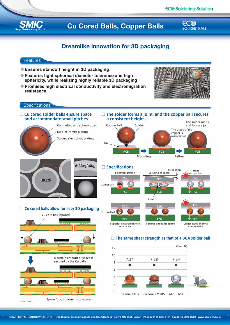
Cu Cored Balls, Copper Balls
Dreamlike innovation for 3D packagingDreamlike innovation for 3D packagingDreamlike innovation for 3D packaging
Features
●
●
●
Ensures standoff height in 3D packagingFeatures tight spherical diameter tolerance and high sphericity, while realizing highly reliable 3D packaging Promises high electrical conductivity and electromigration resistance resistance
Specifications
Cu core ball (spacer)
□ Cu cored solder balls ensure space and accommodate small pitches
PCB
SolderThe solder meltsand forms a joint.
The shape of thecopper ismaintained.
Copper ball
Flux
Mounting Reflow
PCB PCB
□ The solder forms a joint, and the copper ball secures a consistent height.
□ Specifications
PKG
PCBPCB
PKG
PCB
PKG
Solder ball
Cu cored ball
Superior electromagneticresistance
Secures adequate space
Inclination
Short
PCB
PKG
Cu has good thermalconductivity.
PCB
PKG
PCB
PKG
Electromigration Securing of spaceHeat
dissipation
Bump
Shear tool
300um/s
12
10
8
6
4
2
0
7.247.287.24
□ The same shear strength as that of a BGA solder ball
(Unit: N)
Cu core + flux Cu core + M705 M705 ball
Cu ballCu ball
Solder platingSolder plating
Cu ball
Solder plating
□ Cu cored balls allow for easy 3D packaging
A certain amount of space issecured by the Cu balls
Space for components is secured.
Cu: melted and spheroidized
Ni: electrolytic plating
Solder: electrolytic plating