Embed Size (px)
Citation preview
© Digital Integrated Circuits2nd Inverter
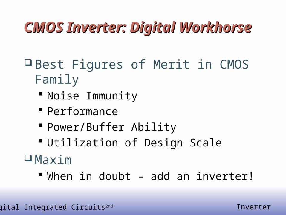
CMOS Inverter: Digital WorkhorseCMOS Inverter: Digital Workhorse
Best Figures of Merit in CMOS Family Noise Immunity Performance Power/Buffer Ability Utilization of Design Scale
Maxim When in doubt – add an inverter!
© Digital Integrated Circuits2nd Inverter
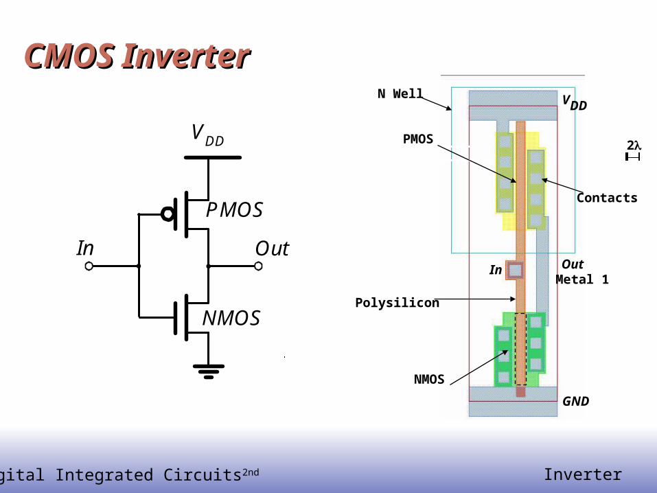
CMOS InverterCMOS Inverter
Polysilicon
In Out
VDD
GND
PMOS 2
Metal 1
NMOS
OutIn
VDD
PMOS
NMOS
Contacts
N Well
© Digital Integrated Circuits2nd Inverter
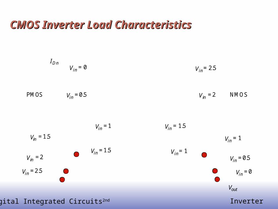
CMOS Inverter Load CharacteristicsCMOS Inverter Load Characteristics
IDn
Vout
Vin = 2.5
Vin = 2
Vin = 1.5
Vin = 0
Vin = 0.5
Vin = 1
NMOS
Vin = 0
Vin = 0.5
Vin = 1Vin = 1.5
Vin = 2
Vin = 2.5
Vin = 1Vin = 1.5
PMOS
© Digital Integrated Circuits2nd Inverter
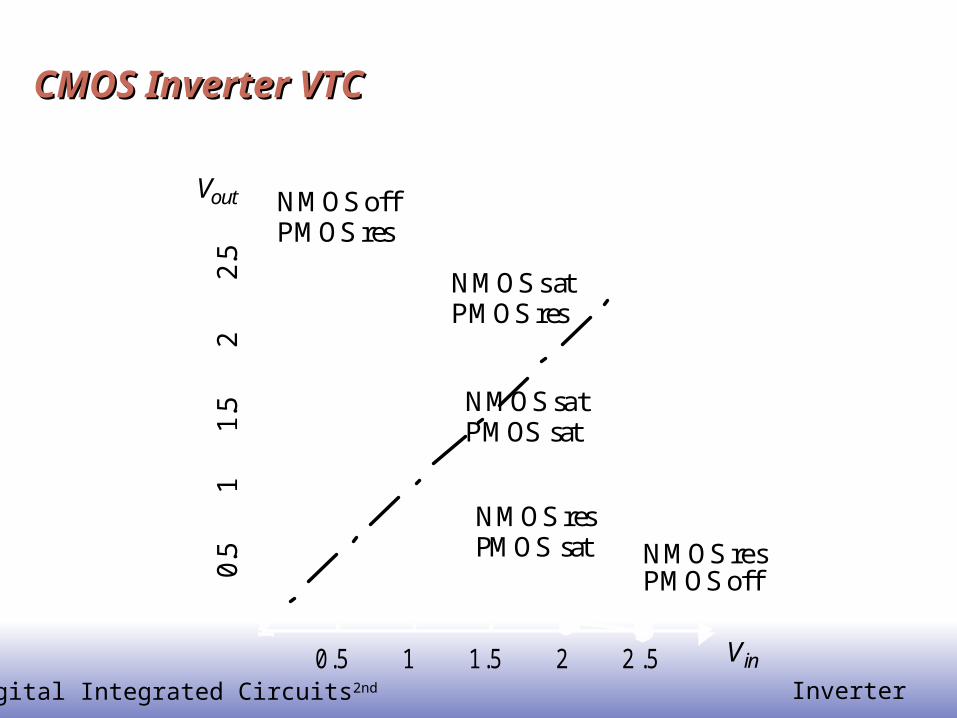
CMOS Inverter VTCCMOS Inverter VTC
Vout
Vin0.5 1 1.5 2 2 .5
0.5
11.
52
2.5
NMOS resPMOS off
NMOS satPMOS sat
NMOS offPMOS res
NMOS satPMOS res
NMOS resPMOS sat

© Digital Integrated Circuits2nd Inverter
Low Frequency Switching Low Frequency Switching Threshold vs. Transistor RatioThreshold vs. Transistor Ratio
100
1010.8
0.9
1
1.1
1.2
1.3
1.4
1.5
1.6
1.7
1.8
MV (
V)
Wp/Wn

© Digital Integrated Circuits2nd Inverter
Inverter GainInverter Gain
0 0.5 1 1.5 2 2.5-18
-16
-14
-12
-10
-8
-6
-4
-2
0
Vin
(V)
gain
© Digital Integrated Circuits2nd Inverter
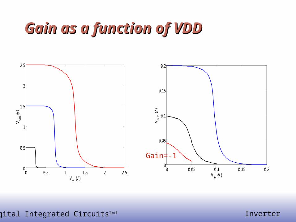
Gain as a function of VDDGain as a function of VDD
0 0.05 0.1 0.15 0.20
0.05
0.1
0.15
0.2
Vin
(V)
Vou
t (V)
0 0.5 1 1.5 2 2.50
0.5
1
1.5
2
2.5
Vin
(V)
Vou
t(V
)
Gain=-1
© Digital Integrated Circuits2nd Inverter
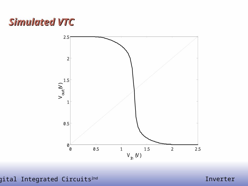
Simulated VTCSimulated VTC
0 0.5 1 1.5 2 2.50
0.5
1
1.5
2
2.5
Vin
(V)
Vou
t(V)
© Digital Integrated Circuits2nd Inverter
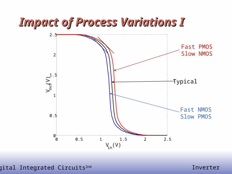
Impact of Process Variations IImpact of Process Variations I
0 0.5 1 1.5 2 2.50
0.5
1
1.5
2
2.5
Vin (V)
Vo
ut(V
)Fast PMOSSlow NMOS
Fast NMOSSlow PMOS
Typical
© Digital Integrated Circuits2nd Inverter
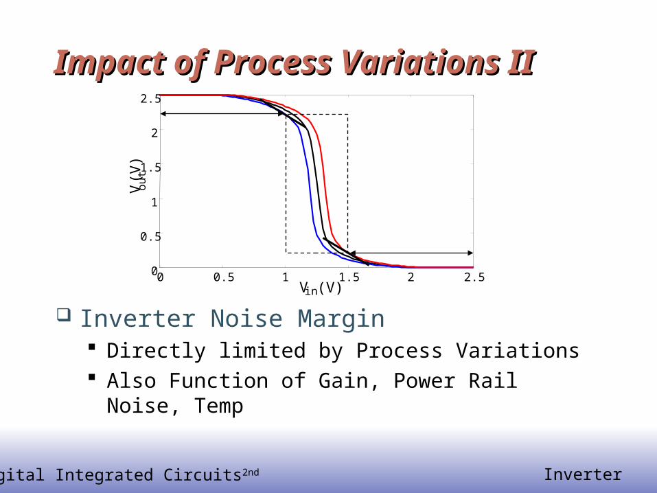
Impact of Process Variations IIImpact of Process Variations II
Inverter Noise Margin Directly limited by Process Variations Also Function of Gain, Power Rail Noise, Temp
0 0.5 1 1.5 2 2.50
0.5
1
1.5
2
2.5
Vin (V)
V ou
t(V)
© Digital Integrated Circuits2nd Inverter
Propagation DelayPropagation Delay
© Digital Integrated Circuits2nd Inverter
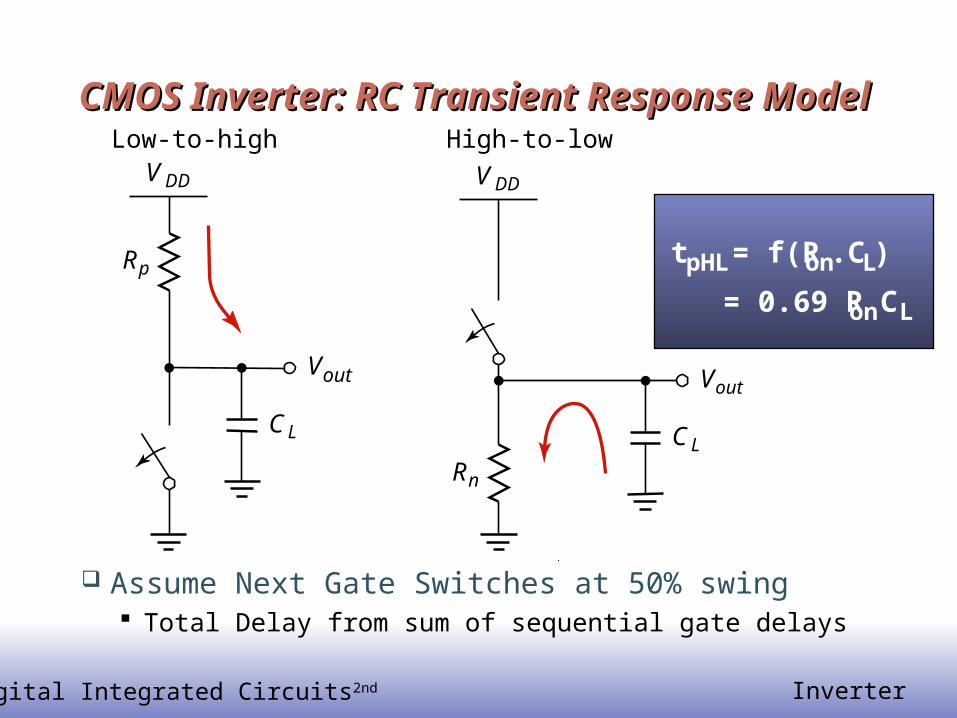
CMOS Inverter: RC Transient Response CMOS Inverter: RC Transient Response ModelModel
Assume Next Gate Switches at 50% swing Total Delay from sum of sequential gate delays
tpHL = f(Ron.CL)
= 0.69 RonCL
VoutVout
Rn
Rp
VDDVDD
Low-to-high High-to-low
CLCL
© Digital Integrated Circuits2nd Inverter
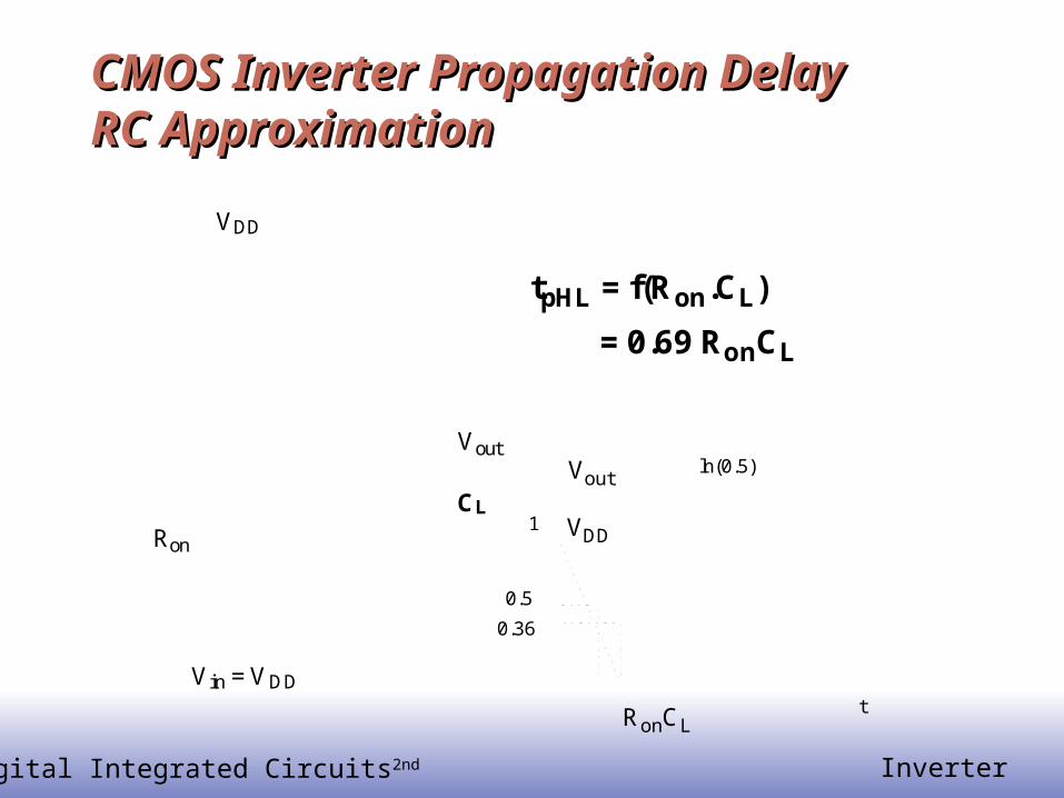
CMOS Inverter Propagation DelayCMOS Inverter Propagation DelayRC ApproximationRC Approximation
VDD
Vout
Vin = VDD
Ron
CL
tpHL = f(Ron.CL)
= 0.69 RonCL
t
Vout
VDD
RonCL
1
0.5
ln(0.5)
0.36
© Digital Integrated Circuits2nd Inverter
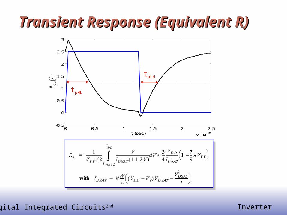
Transient Response (Equivalent R)Transient Response (Equivalent R)
0 0.5 1 1.5 2 2.5
x 10-10
-0.5
0
0.5
1
1.5
2
2.5
3
t (sec)
Vout(V
) tpLH
tpHL

© Digital Integrated Circuits2nd Inverter
CMOS Inverter Propagation DelayCMOS Inverter Propagation DelayHodges ApproximationHodges Approximation
VDD
Vout
Vin = VDD
CLIav
tpHL = CL Vswing/2
Iav
CL
kn VDD
~

© Digital Integrated Circuits2nd Inverter
Transient Model (Equivalent I)Transient Model (Equivalent I)
Hodges Perscription for Iavg: Average of Initial and Final Currents over
swing of interest Easy since you know the voltages in
CMOS: Init=0 or Vdd; Final= Vdd/2 Easy to add effects of other devices,
capacitances and styles since current model
© Digital Integrated Circuits2nd Inverter
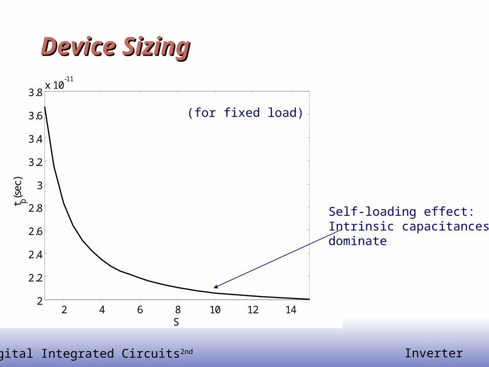
2 4 6 8 10 12 142
2.2
2.4
2.6
2.8
3
3.2
3.4
3.6
3.8x 10
-11
S
t p(sec
)
Device SizingDevice Sizing
(for fixed load)
Self-loading effect:Intrinsic capacitancesdominate
© Digital Integrated Circuits2nd Inverter
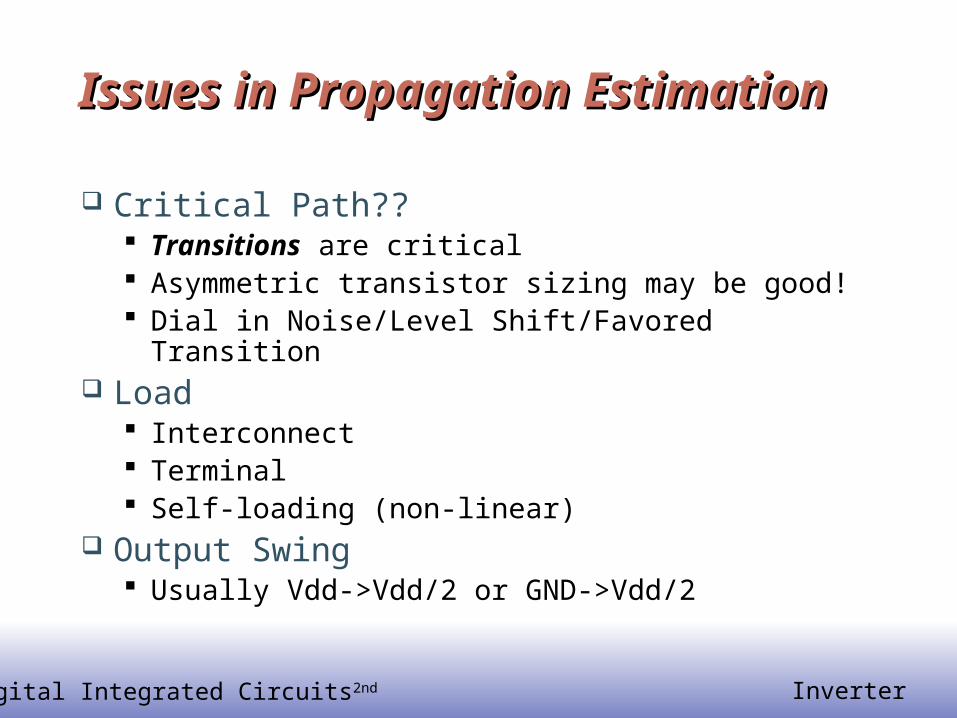
Issues in Propagation EstimationIssues in Propagation Estimation
Critical Path?? Transitions are critical Asymmetric transistor sizing may be good! Dial in Noise/Level Shift/Favored Transition
Load Interconnect Terminal Self-loading (non-linear)
Output Swing Usually Vdd->Vdd/2 or GND->Vdd/2

© Digital Integrated Circuits2nd Inverter
1 1.5 2 2.5 3 3.5 4 4.5 53
3.5
4
4.5
5x 10
-11
t p(sec
)
NMOS/PMOS ratioNMOS/PMOS ratio
tpLH tpHL
tp = Wp/Wn
© Digital Integrated Circuits2nd Inverter
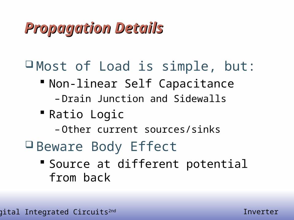
Propagation DetailsPropagation Details
Most of Load is simple, but: Non-linear Self Capacitance
– Drain Junction and Sidewalls
Ratio Logic– Other current sources/sinks
Beware Body Effect Source at different potential from back
© Digital Integrated Circuits2nd Inverter
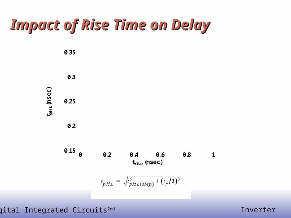
Impact of Rise Time on DelayImpact of Rise Time on Delayt p
HL(n
sec
)0.35
0.3
0.25
0.2
0.15
trise (nsec)10.80.60.40.20
© Digital Integrated Circuits2nd Inverter
Inverter SizingInverter Sizing
© Digital Integrated Circuits2nd Inverter
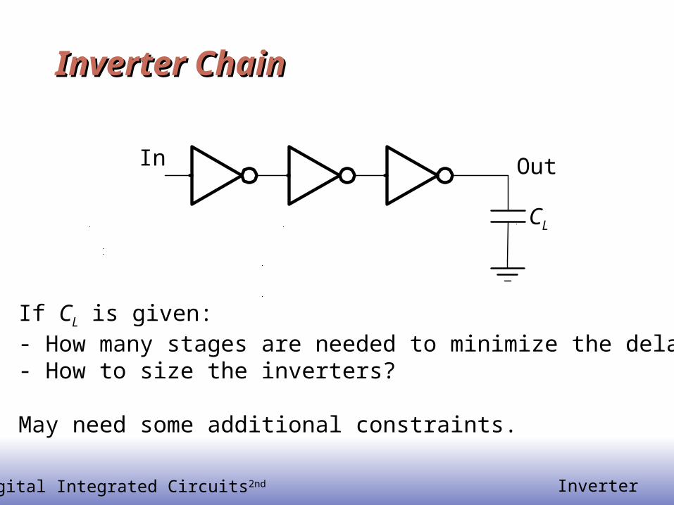
Inverter ChainInverter Chain
CL
If CL is given:- How many stages are needed to minimize the delay?- How to size the inverters?
May need some additional constraints.
In Out
© Digital Integrated Circuits2nd Inverter
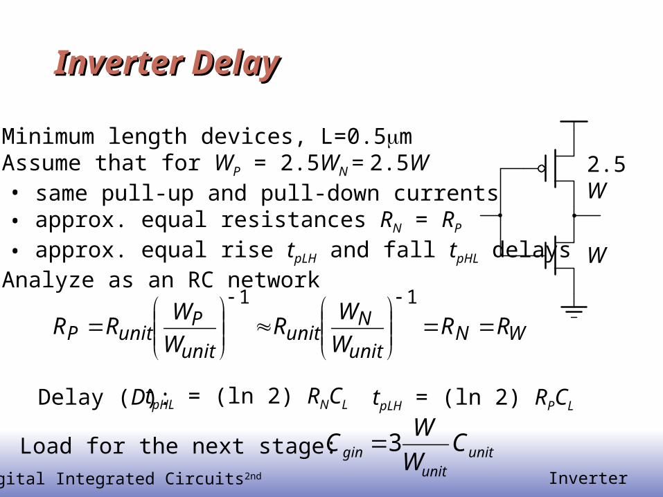
Inverter DelayInverter Delay
• Minimum length devices, L=0.5m• Assume that for WP = 2.5WN = 2.5W
• same pull-up and pull-down currents• approx. equal resistances RN = RP
• approx. equal rise tpLH and fall tpHL delays• Analyze as an RC network
WNunit
Nunit
unit
PunitP RR
W
WR
W
WRR
11
tpHL = (ln 2) RNCL tpLH = (ln 2) RPCLDelay (D):
2.5W
W
unitunit
gin CW
WC 3Load for the next stage:
© Digital Integrated Circuits2nd Inverter
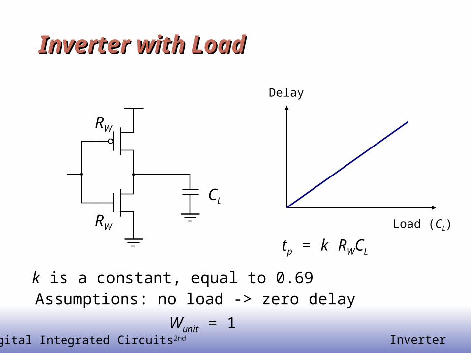
Inverter with LoadInverter with Load
Load (CL)
Delay
Assumptions: no load -> zero delay
CL
tp = k RWCL
RW
RW
Wunit = 1
k is a constant, equal to 0.69

© Digital Integrated Circuits2nd Inverter
Inverter with LoadInverter with Load
Load
Delay
Cint CL
Delay = kRW(Cint + CL) = kRWCint + kRWCL = kRW Cint(1+ CL /Cint)= Delay (Internal) + Delay (Load)
CN = Cunit
CP = 2.5Cunit
2.5W
W
© Digital Integrated Circuits2nd Inverter
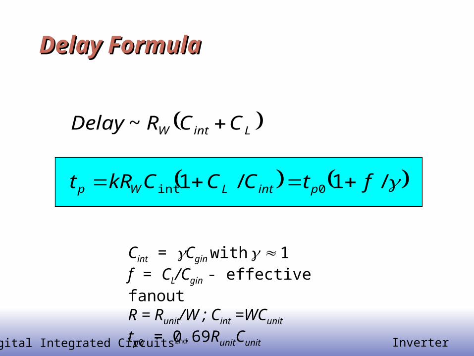
Delay FormulaDelay Formula
/1/1
~
0int ftCCCkRt
CCRDelay
pintLWp
LintW
Cint = Cgin with 1f = CL/Cgin - effective fanoutR = Runit/W ; Cint =WCunit
tp0 = 0.69RunitCunit
© Digital Integrated Circuits2nd Inverter
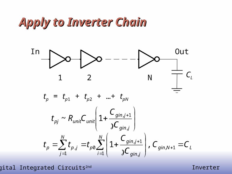
Apply to Inverter ChainApply to Inverter Chain
CL
In Out
1 2 N
tp = tp1 + tp2 + …+ tpN
jgin
jginunitunitpj C
CCRt
,
1,1~
LNgin
N
i jgin
jginp
N
jjpp CC
C
Cttt
1,
1 ,
1,0
1, ,1
© Digital Integrated Circuits2nd Inverter
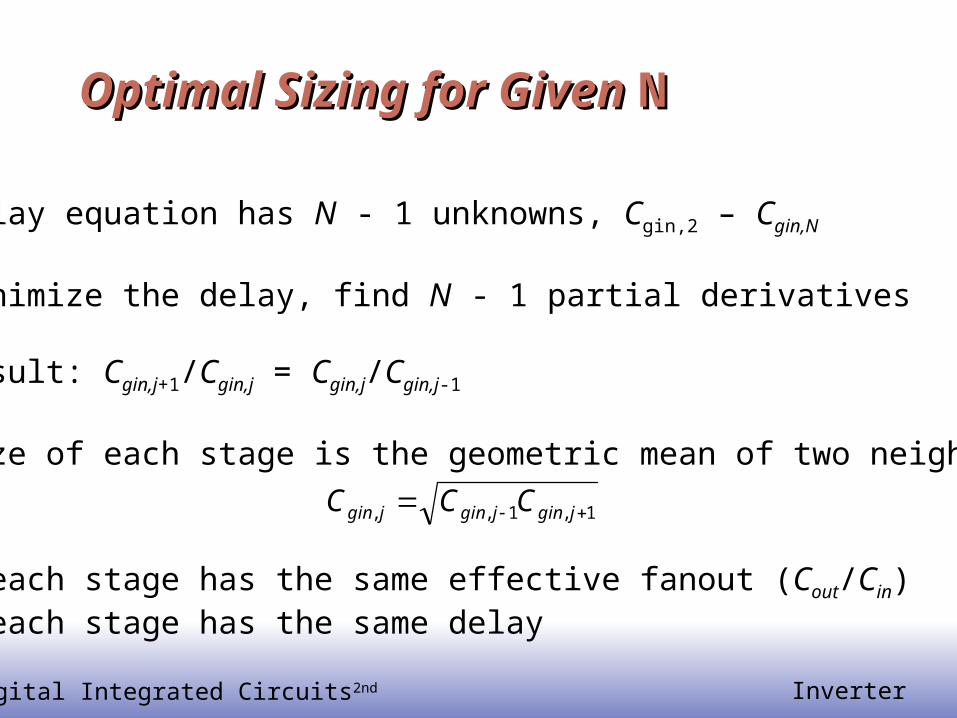
Optimal Sizing for Given Optimal Sizing for Given NN
Delay equation has N - 1 unknowns, Cgin,2 – Cgin,N
Minimize the delay, find N - 1 partial derivatives
Result: Cgin,j+1/Cgin,j = Cgin,j/Cgin,j-1
Size of each stage is the geometric mean of two neighbors
- each stage has the same effective fanout (Cout/Cin)- each stage has the same delay
1,1,, jginjginjgin CCC
© Digital Integrated Circuits2nd Inverter
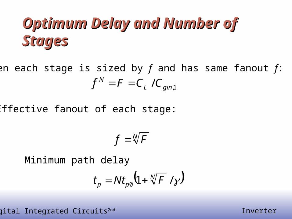
Optimum Delay and Number of Optimum Delay and Number of StagesStages
1,/ ginLN CCFf
When each stage is sized by f and has same fanout f:
N Ff
/10N
pp FNtt
Minimum path delay
Effective fanout of each stage:
© Digital Integrated Circuits2nd Inverter
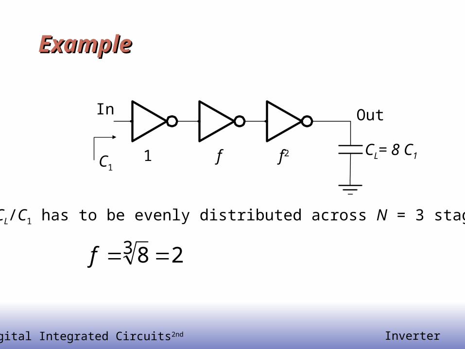
ExampleExample
CL= 8 C1
In Out
C11 f f2
283 f
CL/C1 has to be evenly distributed across N = 3 stages:
© Digital Integrated Circuits2nd Inverter
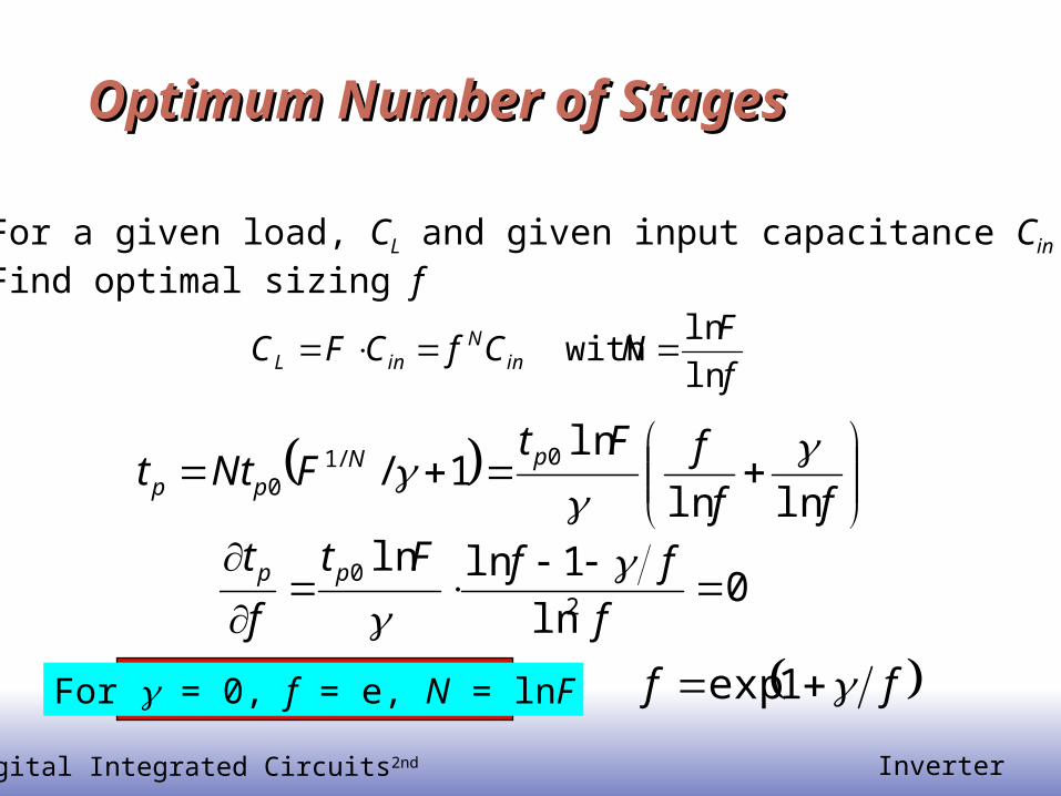
Optimum Number of StagesOptimum Number of Stages
For a given load, CL and given input capacitance Cin
Find optimal sizing f
ff
fFtFNtt pN
pp lnln
ln1/ 0/1
0
0ln
1lnln2
0
f
ffFt
f
t pp
For = 0, f = e, N = lnF
f
FNCfCFC in
NinL ln
ln with
ff 1exp
© Digital Integrated Circuits2nd Inverter
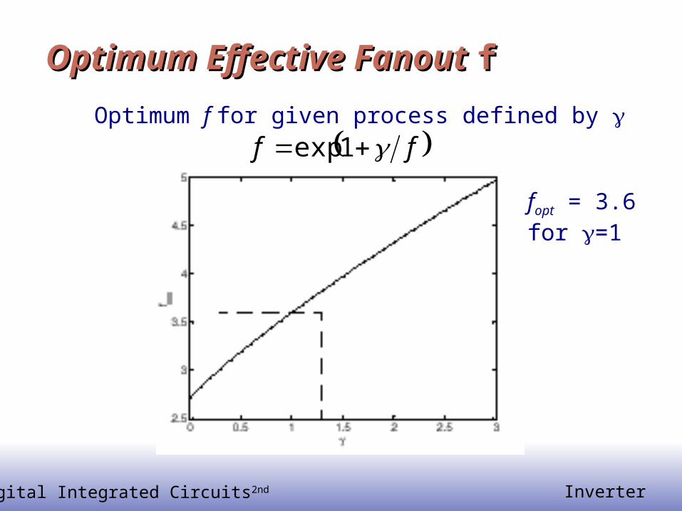
Optimum Effective Fanout Optimum Effective Fanout ff
Optimum f for given process defined by ff 1exp
fopt = 3.6for =1
© Digital Integrated Circuits2nd Inverter
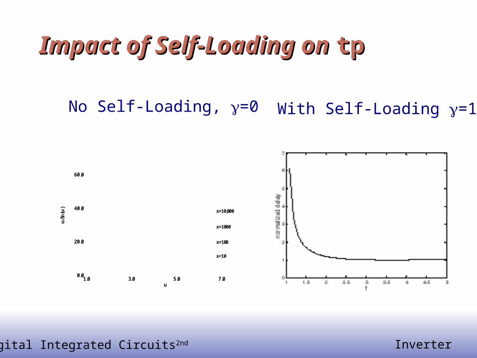
Impact of Self-Loading on Impact of Self-Loading on tptp
1.0 3.0 5.0 7.0u
0.0
20.0
40.0
60.0
u/l
n(u
)
x=10
x=100
x=1000
x=10,000
No Self-Loading, =0 With Self-Loading =1
© Digital Integrated Circuits2nd Inverter
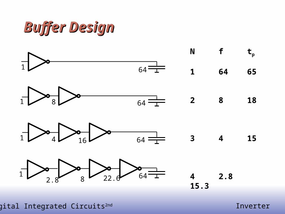
Buffer DesignBuffer Design
1
1
1
1
8
64
64
64
64
4
2.8 8
16
22.6
N f tp
1 64 65
2 8 18
3 4 15
4 2.8 15.3
© Digital Integrated Circuits2nd Inverter
Power DissipationPower Dissipation

© Digital Integrated Circuits2nd Inverter
Where Does Power Go in CMOS?Where Does Power Go in CMOS?
• Dynamic Power Consumption
• Short Circuit Currents
• Leakage
Charging and Discharging Capacitors
Short Circuit Path between Supply Rails during Switching
Leaking diodes and transistors

© Digital Integrated Circuits2nd Inverter
Dynamic Power DissipationDynamic Power Dissipation
Energy/transition = CL * Vdd2
Power = Energy/transition * f = CL * Vdd2 * f
Need to reduce CL, Vdd, and f to reduce power.
Vin Vout
CL
Vdd
Not a function of transistor sizes!
© Digital Integrated Circuits2nd Inverter
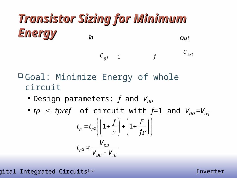
Transistor Sizing for Minimum Transistor Sizing for Minimum EnergyEnergy
Goal: Minimize Energy of whole circuit Design parameters: f and VDD
tp tpref of circuit with f=1 and VDD =Vref
1Cg1
In
fCext
Out
TEDD
DDp
pp
VV
Vt
f
Fftt
0
0 11

© Digital Integrated Circuits2nd Inverter
Transistor Sizing (2)Transistor Sizing (2) Performance Constraint (=1)
Energy for single Transition
13
2
3
2
0
0
F
fF
f
VV
VV
V
V
F
fF
f
t
t
t
t
TEDD
TEref
ref
DD
refp
p
pref
p
F
Ff
V
V
E
E
FfCVE
ref
DD
ref
gDD
4
22
112
12
© Digital Integrated Circuits2nd Inverter
1 2 3 4 5 6 70
0.5
1
1.5
2
2.5
3
3.5
4
f
vdd
(V
)
1 2 3 4 5 6 70
0.5
1
1.5
f
no
rma
lize
d e
ne
rgy
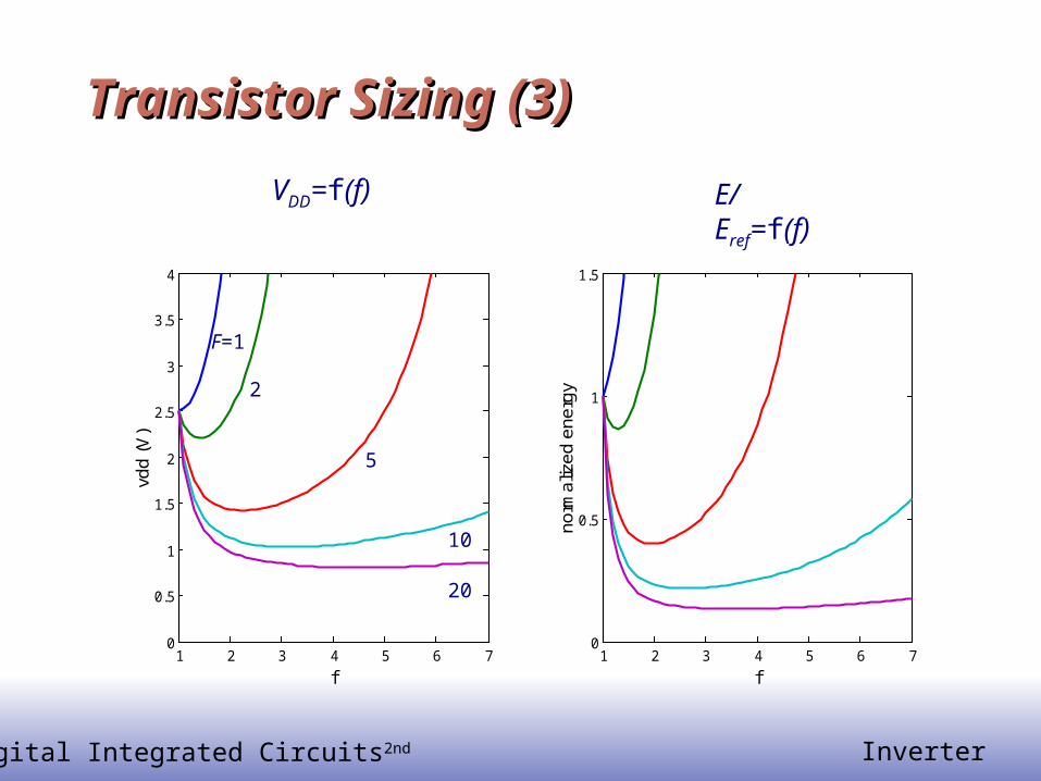
Transistor Sizing (3)Transistor Sizing (3)
F=1
2
5
10
20
VDD=f(f) E/Eref=f(f)
© Digital Integrated Circuits2nd Inverter
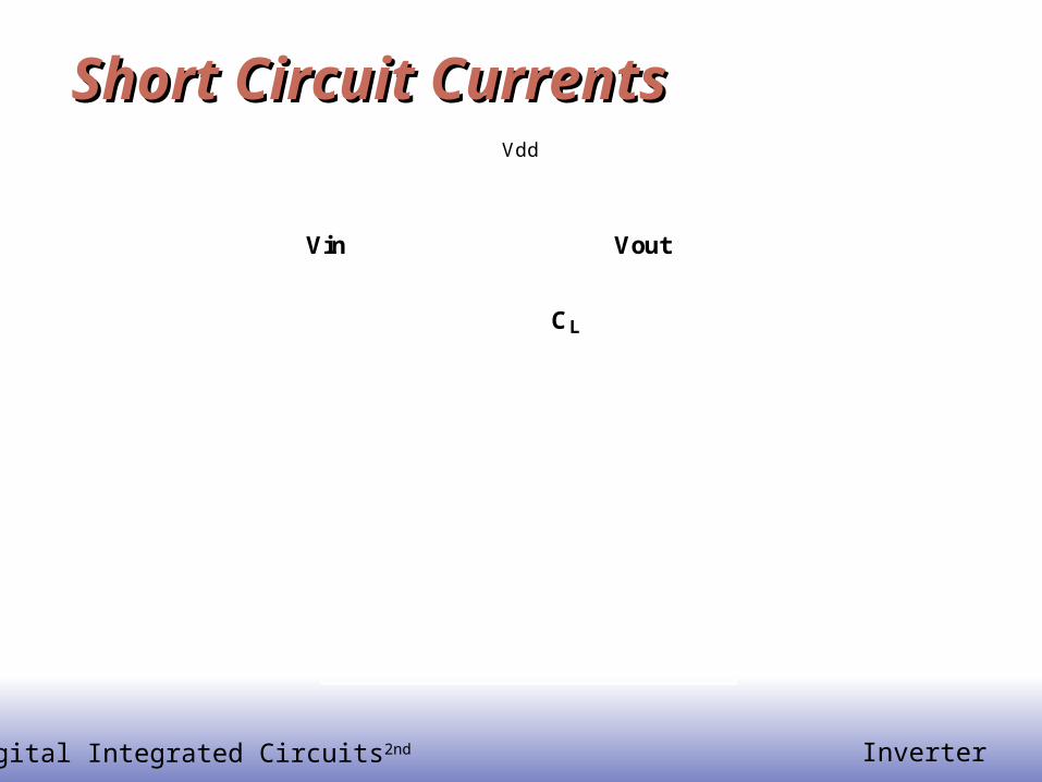
Short Circuit CurrentsShort Circuit Currents
Vin Vout
CL
Vdd
I VD
D (m
A)
0.15
0.10
0.05
Vin (V)5.04.03.02.01.00.0

© Digital Integrated Circuits2nd Inverter
How to keep Short-Circuit Currents Low?How to keep Short-Circuit Currents Low?
Short circuit current goes to zero if tfall >> trise,but can’t do this for cascade logic, so ...

© Digital Integrated Circuits2nd Inverter
Minimizing Short-Circuit PowerMinimizing Short-Circuit Power
0 1 2 3 4 50
1
2
3
4
5
6
7
8
tsin
/tsout
Pno
rm
Vdd =1.5
Vdd =2.5
Vdd =3.3
© Digital Integrated Circuits2nd Inverter
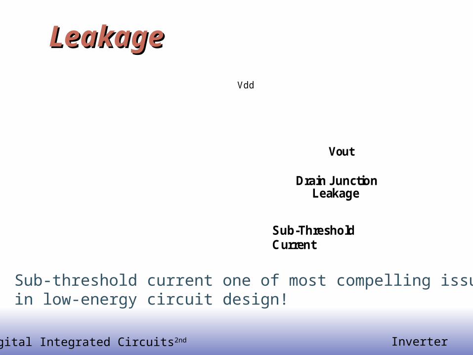
LeakageLeakage
Vout
Vdd
Sub-ThresholdCurrent
Drain JunctionLeakage
Sub-Threshold Current Dominant FactorSub-threshold current one of most compelling issuesin low-energy circuit design!

© Digital Integrated Circuits2nd Inverter
Reverse-Biased Diode LeakageReverse-Biased Diode Leakage
Np+ p+
Reverse Leakage Current
+
-Vdd
GATE
IDL = JS A
JS = 1-5pA/m2 for a 1.2m CMOS technology
Js double with every 9oC increase in temperature
JS = 10-100 pA/m2 at 25 deg C for 0.25m CMOSJS doubles for every 9 deg C!

© Digital Integrated Circuits2nd Inverter
Subthreshold Leakage ComponentSubthreshold Leakage Component
© Digital Integrated Circuits2nd Inverter
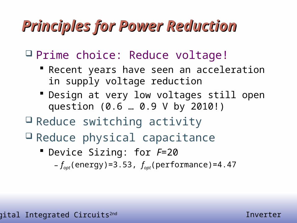
Principles for Power ReductionPrinciples for Power Reduction
Prime choice: Reduce voltage! Recent years have seen an acceleration in supply
voltage reduction Design at very low voltages still open question (0.6
… 0.9 V by 2010!)
Reduce switching activity Reduce physical capacitance
Device Sizing: for F=20– fopt(energy)=3.53, fopt(performance)=4.47