Embed Size (px)
Citation preview

TPS65276V
www.ti.com SLVSBW0B –FEBRUARY 2013–REVISED JANUARY 2014
4.5-V TO 18-V INPUT VOLTAGE, 6-A/3.5-A DUAL SYNCHRONOUS STEP-DOWNCONVERTER WITH I2C CONTROLLED VID
Check for Samples: TPS65276V
1FEATURES• 4.5-V to 18-V Wide Input Voltage Range • Peak Current-Mode Control with Simple
Compensation Circuit• I2C Controlled 7-Bits VID ProgrammableOutput Voltage from 0.68 V to 1.95 V with • Cycle-by-Cycle Over Current Protection10-mV Steps for Each Buck; Output Voltage • 180° Out-of-Phase Operation to Reduce InputCan Also be Set By Resistor Divider Capacitance and Power Supply Induced Noise
• Programmable Slew Rate Control for Output • Over Temperature ProtectionVoltage Transition • Available in 32-Pin Thermally Enhanced
• Up to 6-A Maximum Continuous Output HTSSOP (DAP) and 36-Pin QFN 6-mm x 6-mmCurrent in Buck 1 and 3.5-A in Buck 2 (RHH) Packages
• I2C Compatible Interface With Standard Mode(100 kHz) and Fast Mode (400 kHz) APPLICATIONS
• I2C Read Back Power Good Status and Die • DTVTemperature Warning • TCON
• Pulse Skipping Mode to Achieve High • BDVDEfficiency in Light Load • Set Top Boxes
• Adjustable Switching Frequency • Tablet PC200 kHz - 1.6 MHz Set by External Resistor• Dedicated Enable and Soft-Start for Each Buck
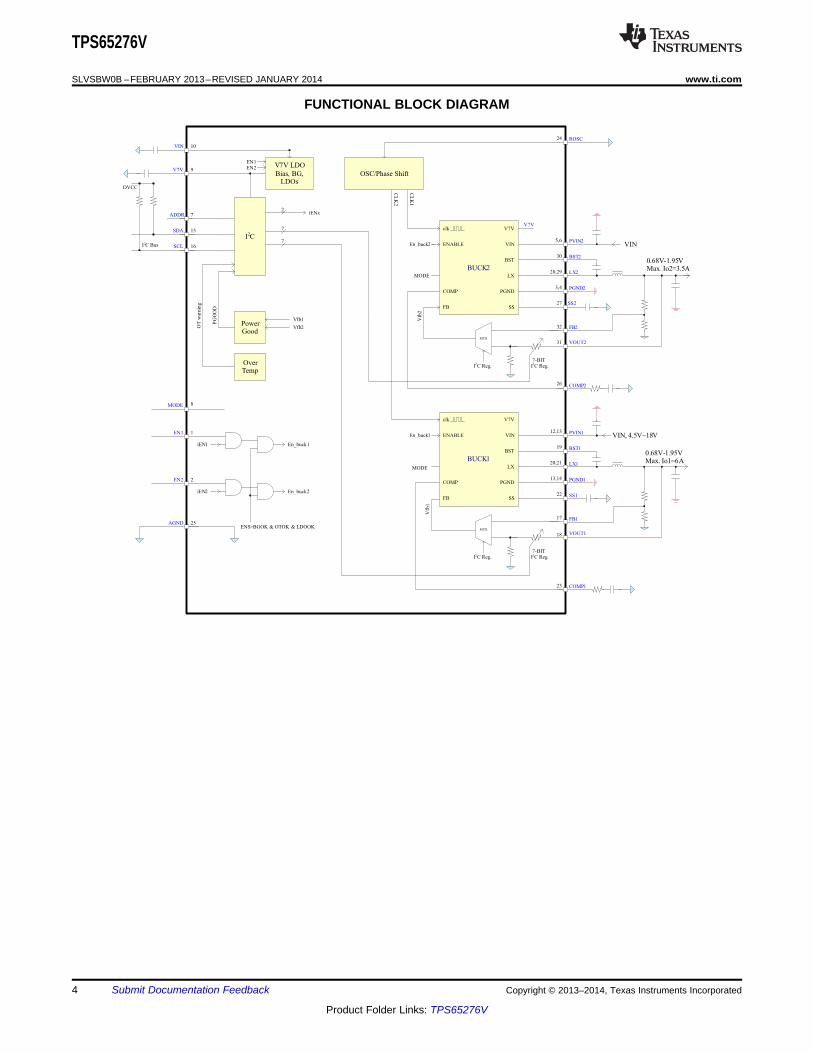
DESCRIPTION/ORDERING INFORMATIONTPS65276V is a monolithic dual synchronous buck converter with wide 4.5V to 18V operating input voltagerange that encompassed most intermediate bus voltage operating off 5-, 9-, 12- or 15-V power bus or battery.The converter with constant frequency peak current mode control is designed to simplify its application whilegiving the designers options to optimize their usage according to the target applications.
Each buck converter in TPS65276V has external feedback resistors that can be used for setting the initial startup voltage. The feedback voltage reference for this start-up option is 0.6 V. Once the VID DAC is updated via theI2C, the buck converter switches feedback resistors from external to internal. The output voltage in each buckcan be programmable from 0.68 V to 1.95 V in 10-mV steps with I2C Controlled 7-Bits VID.
Each buck converter in TPS65276V can also be I2C controlled for enabling/disabling output voltage, setting thepulse skipping mode and reading the power good status and die temperature warning.
The switching frequency of the converters can be set from 200 kHz to 1.6 MHz with an external resistor. Twoconverters have clock signal with 180° out-of-phase.
TPS65276V features dedicated enable pin when I2C interface is not used. Independent soft-start pin providesflexibility in power up programmability. Constant frequency peak current mode control simplifies thecompensation and provides fast transient response. Cycle-by-cycle over current protection and hiccup modeoperation limit MOSFET power dissipation in short circuit or over loading fault conditions. Low side reverse overcurrent protection also prevents excessive sinking current from damaging the converter.
TPS65273V also features a light load pulse skipping mode (PSM) that can be controlled by I2C or MODE pinconfiguration. The PSM mode allows a power loss reduction on the input power supplied to the system toachieve high efficiency at light loading.
The TPS65273V is available in a 32-pin thermally enhanced HTSSOP (DAP) package and 36-pin QFN6-mm x 6-mm (RHH) package.1
Please be aware that an important notice concerning availability, standard warranty, and use in critical applications ofTexas Instruments semiconductor products and disclaimers thereto appears at the end of this data sheet.
PRODUCTION DATA information is current as of publication date. Copyright © 2013–2014, Texas Instruments IncorporatedProducts conform to specifications per the terms of the TexasInstruments standard warranty. Production processing does notnecessarily include testing of all parameters.

TPS65276V
SLVSBW0B –FEBRUARY 2013–REVISED JANUARY 2014 www.ti.com
ORDERING INFORMATION (1)
TA PACKAGE (2) ORDERABLE PART NUMBER TOP-SIDE MARKING32-pin HTSSOP (DAP) TPS65276VDAPR
–40°C to 85°C TPS65276V36-pin QFN (RHH) TPS65276VRHHR
(1) For the most current package and ordering information, see the Package Option Addendum at the end of this document, or see the TIweb site at www.ti.com.
(2) Package drawings, thermal data, and symbolization are available at www.ti.com/packaging.
2 Submit Documentation Feedback Copyright © 2013–2014, Texas Instruments Incorporated
Product Folder Links: TPS65276V

EN1
PGND2
PGND2
PVIN2
PVIN2
ADDR
MODE
V7V
VIN
PVIN1
EN2
PVIN1
FB2
VOUT2
BST2
LX2
LX2
SS2
COMP2
AGND
ROSC
COMP1
SS1
LX1
PGND1
PGND1
LX1
BST1
1
2
3
5
6
7
8
9
10
11
12
13
14
28
29
30
31
32
21
22
23
24
25
26
27
19
20
L1
4.7uH
C19
47nF
VOUT1=0.68V~1.95V
Res. = 10mVMax. Io1=6A
Power Ground Analog Ground
C22
C9
1uF
R16
10K
R15
10K
C14
10uF
DVCC
SCL
SDA
R23 C23VIN4.5V~18V
VOUT1
FB1
17
18
SDA
SCL
15
16
Power Pad
4
C20
5x22uF
R17
R18C18
C3
10uF
R2
100K
R1
100K
L2
4.7uH
C30
47nF
VOUT2=0.68V~1.95V
Res. = 10mVMax. Io1=3.5A
C27
C29
5x22uF
R32
R31C31
C26R26
R24
33
TPS65276V
www.ti.com SLVSBW0B –FEBRUARY 2013–REVISED JANUARY 2014
This integrated circuit can be damaged by ESD. Texas Instruments recommends that all integrated circuits be handled withappropriate precautions. Failure to observe proper handling and installation procedures can cause damage.
ESD damage can range from subtle performance degradation to complete device failure. Precision integrated circuits may be moresusceptible to damage because very small parametric changes could cause the device not to meet its published specifications.
TYPICAL APPLICATION
Figure 1. Dual Mode Operation to Deliver 6 A at Buck 1 and 3.5 A at Buck 2
Copyright © 2013–2014, Texas Instruments Incorporated Submit Documentation Feedback 3
Product Folder Links: TPS65276V
PVIN2
BUCK2
ENABLE
FB
COMP
clk V7V
VIN
BST
LX
PGND
BST2
LX2
PGND2
PVIN1
BST1
LX1
PGND1
BUCK1
ENABLE
COMP
FB
clk V7V
VIN
BST
LX
PGND
I2C
ADDR
SDA
SCL
OSC/Phase Shift
V7V LDO
Bias, BG,LDOs
V7V
iENx
COMP2
FB1
COMP1
FB2
CL
K1
CL
K2
VIN
0.68V-1.95VMax. Io2=3.5A
VIN, 4.5V~18V
En_buck2
En_buck1
7
2
PowerGood
Vfb
1
Vfb
2
AGND
Vfb1
Vfb2
DVCC
VIN 10
9
7
15
16
25
23
13,14
20,21
19
12,13
31
32
3,4
28,29
30
5,6
OverTemp
PG
OO
D
OT
war
nin
g
En_buck1iEN1
En_buck2iEN2
ENS=BGOK & OTOK & LDOOK
EN1
EN2
1
2
7
SS27
SS22
ROSC24
V7V
MUX
VOUT2
7-BITI2C Reg. I
2C Reg.
0.68V-1.95VMax. Io1=6A
18
17
MUX
VOUT1
7-BITI2C Reg. I2C Reg.
EN1EN2
MODE
MODE
MODE
8
SS2
26
SS1
I2C Bus
TPS65276V
SLVSBW0B –FEBRUARY 2013–REVISED JANUARY 2014 www.ti.com
FUNCTIONAL BLOCK DIAGRAM
4 Submit Documentation Feedback Copyright © 2013–2014, Texas Instruments Incorporated
Product Folder Links: TPS65276V
Power Pad
2
PGND1
3
PVIN2
4
SDA
5
V7V
6
MODE
7
8
9
VIN
10
PGND2
11
12
13
31
PGND2
30
BST2
29
LX2
28
LX2
27
SS2
26
COMP1
25
SS1
24
LX1
23
LX1
22
PGND1
21
BST1
20
VOUT2
PVIN1
EN2
VOUT1
14
15
19
18
COMP2
FB2
ROSC
SCL
PVIN1
PVIN2
ADDR
EN1
16 17
1 32
FB1
AGND
TPS65276V
www.ti.com SLVSBW0B –FEBRUARY 2013–REVISED JANUARY 2014
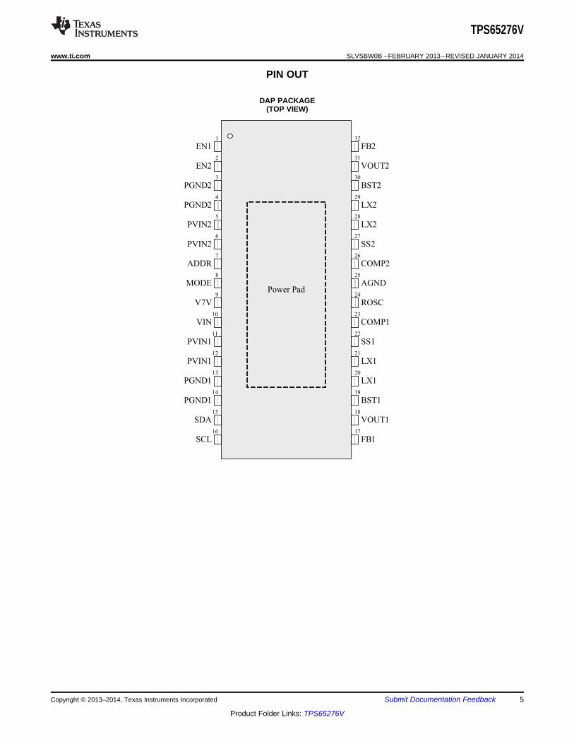
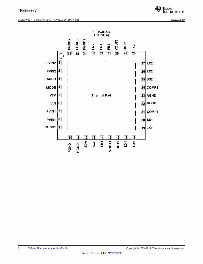
PIN OUT
DAP PACKAGE(TOP VIEW)
Copyright © 2013–2014, Texas Instruments Incorporated Submit Documentation Feedback 5
Product Folder Links: TPS65276V
PG
ND
1
SC
L
FB
1
LX1
VO
UT
1COMP1
SS1
FB
2
VO
UT
2
PVIN2 1
2
3
4
5
6
11 12 13 14 15 16
EN
2
EN
1
PVIN2P
GN
D2
ROSC
24
23
22
21
20
PG
ND
2
25
34 33 32 31 30
ADDR
SD
A
PG
ND
1
MODE
Thermal Pad
BS
T1
17
V7V
VIN
PVIN1 7
8
9
PVIN1
PGND1
SS2
LX2
LX2
27
26
COMP2
AGND
BS
T2
28
10 18
LX
1
LX
1
19
29
LX
2
36
PG
ND
2
35
TPS65276V
SLVSBW0B –FEBRUARY 2013–REVISED JANUARY 2014 www.ti.com
RHH PACKAGE(TOP VIEW)
6 Submit Documentation Feedback Copyright © 2013–2014, Texas Instruments Incorporated
Product Folder Links: TPS65276V

TPS65276V
www.ti.com SLVSBW0B –FEBRUARY 2013–REVISED JANUARY 2014
TERMINAL FUNCTIONSNO. NO.NAME DESCRIPTION(HTSSOP) (QFN)
EN1, EN2 1, 2 32, 33 Enable pin. Adjust the input under-voltage lockout with two resistors.PGND2 3, 4 34, 35, 36 Power ground of Buck 2, place the input capacitor’s ground pin as close
as possible to this pin.PVIN2 5, 6 1, 2 Power input. Input power supply to the power switches of the power
converter 2.ADDR 7 3 I2C address configuration pin. Connect this pin to low, high or leave it
open to select different I2C slave address.MODE 8 4 Operation mode control pin. Connect this pin to ground to choose forced
PWM mode without current sharing; leave the pin open for pulse skippingmode (PSM) operation at light load condition; connect this pin to V7V tochoose forced PWM mode and current sharing with paralleling two bucks.
V7V 9 5 Internal low-drop linear regulator (LDO) output to power internal driverand control circuits. Decouple this pin to power ground with a minimum1-µF ceramic capacitor. Output regulates to typical 6.3 V for optimalconduction on-resistances of internal power MOSFETs. In PCB design,the power ground and analog ground should have one-point commonconnection at the (-) terminal of V7V bypass capacitor. If VIN is lowerthan 6.3 V, V7V will be slightly lower than VIN.
VIN 10 6 Power supply of the internal LDO and controllersPVIN1 11, 12 7, 8 Power input. Input power supply to the power switches of the power
converter 1.PGND1 13, 14 9, 10, 11 Power ground of Buck 1, place the input capacitor’s ground pin as close
as possible to this pin.SDA 15 12 I2C interface data pinSCL 16 13 I2C interface clock pinFB1 17 14 Feedback sensing pin for the external feedback resistors in Buck 1.
Before I2C controlled VID selection is enabled, an external resistor dividerconnects to this pin to pre-set the output voltage.
VOUT1 18 15 Buck 1 output voltage sensing pin; When I2C controlled VID selection isenabled, output voltage can be programmed from 0.68 V to 1.95 V with10-mV steps. In current sharing application, this pin is the output voltagesensing pin.
BST1 19 16 Add a bootstrap capacitor between BST1 and LX1. The voltage on thiscapacitor carries the gate drive voltage for the high-side MOSFET.
LX1 20, 21 17, 18, 19 Switching node of Buck 1SS1 22, 27 20, 25 Soft-start and voltage tracking in Buck 1. An external capacitor connected
to this pin sets the internal voltage reference rise time. Since the voltageon this pin overrides the internal reference, it can be used for tracking andsequencing. In current sharing application, this pin serves as the soft-startpin.
COMP1 23 21 Error amplifier output and loop compensation pin for Buck 1. Connectfrequency compensation to this pin; In current sharing application, this pinserves as the compensation pin.
ROSC 24 22 Oscillator frequency programmable pin. Connect an external resistor toset the switching frequency. When connected to an external clock, theinternal oscillator synchronizes to the external clock.
AGND 25 23 Analog ground of the controllersCOMP2 26 24 Error amplifier output and loop compensation pin for Buck 2. Connect
frequency compensation to this pin. In current sharing application,connect this pin to ground.
SS2 27 25 Soft-start and voltage tracking in Buck 2. An external capacitor connectedto this pin sets the internal voltage reference rise time. Since the voltageon this pin overrides the internal reference, it can be used for tracking andpower sequencing. In current sharing application, connect this pin toground.
LX2 28, 29 26, 27, 28 Switching nodes
Copyright © 2013–2014, Texas Instruments Incorporated Submit Documentation Feedback 7
Product Folder Links: TPS65276V
TPS65276V
SLVSBW0B –FEBRUARY 2013–REVISED JANUARY 2014 www.ti.com
TERMINAL FUNCTIONS (continued)NO. NO.NAME DESCRIPTION(HTSSOP) (QFN)
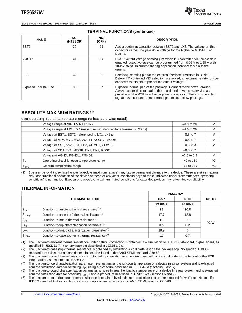
BST2 30 29 Add a bootstrap capacitor between BST2 and LX2. The voltage on thiscapacitor carries the gate drive voltage for the high-side MOSFET ofBuck 2.
VOUT2 31 30 Buck 2 output voltage sensing pin; When I2C controlled VID selection isenabled, output voltage can be programmed from 0.68 V to 1.95 V with10-mV steps. In current sharing application, connect this pin to theground.
FB2 32 31 Feedback sensing pin for the external feedback resistors in Buck 2.Before I2C controlled VID selection is enabled, an external resistor dividerconnects to this pin to pre-set the output voltage.
Exposed Thermal Pad 33 37 Exposed thermal pad of the package. Connect to the power ground.Always solder thermal pad to the board, and have as many vias aspossible on the PCB to enhance power dissipation. There is no electricsignal down bonded to the thermal pad inside the IC package.
ABSOLUTE MAXIMUM RATINGS (1)
over operating free-air temperature range (unless otherwise noted)Voltage range at VIN, PVIN1,PVIN2 –0.3 to 20 VVoltage range at LX1, LX2 (maximum withstand voltage transient < 20 ns) –4.5 to 20 VVoltage at BST1, BST2, referenced to LX1, LX2 pin –0.3 to 7 VVoltage at V7V, EN1, EN2, VOUT1, VOUT2, MODE –0.3 to 7 VVoltage at SS1, SS2, FB1, FB2, COMP1, COMP2 –0.3 to 3 VVoltage at SDA, SCL, ADDR, EN1, EN2, ROSC –0.3 to 7Voltage at AGND, PGND1, PGND2 –0.3 to 0.3 V
TJ Operating virtual junction temperature range –40 to 150 °CTSTG Storage temperature range –55 to 150 °C
(1) Stresses beyond those listed under "absolute maximum ratings" may cause permanent damage to the device. These are stress ratingsonly, and functional operation of the device at these or any other conditions beyond those indicated under "recommended operatingconditions" is not implied. Exposure to absolute–maximum–rated conditions for extended periods may affect device reliability.
THERMAL INFORMATIONTPS65276V
THERMAL METRIC DAP RHH UNITS32 PINS 36 PINS
θJA Junction-to-ambient thermal resistance (1) 35 30.8θJCtop Junction-to-case (top) thermal resistance (2) 17.7 18.8θJB Junction-to-board thermal resistance (3) 19 6
°C/WψJT Junction-to-top characterization parameter (4) 0.5 0.2ψJB Junction-to-board characterization parameter (5) 18.9 6θJCbot Junction-to-case (bottom) thermal resistance (6) 1.3 0.7
(1) The junction-to-ambient thermal resistance under natural convection is obtained in a simulation on a JEDEC-standard, high-K board, asspecified in JESD51-7, in an environment described in JESD51-2a.
(2) The junction-to-case (top) thermal resistance is obtained by simulating a cold plate test on the package top. No specific JEDEC-standard test exists, but a close description can be found in the ANSI SEMI standard G30-88.
(3) The junction-to-board thermal resistance is obtained by simulating in an environment with a ring cold plate fixture to control the PCBtemperature, as described in JESD51-8.
(4) The junction-to-top characterization parameter, ψJT, estimates the junction temperature of a device in a real system and is extractedfrom the simulation data for obtaining θJA, using a procedure described in JESD51-2a (sections 6 and 7).
(5) The junction-to-board characterization parameter, ψJB, estimates the junction temperature of a device in a real system and is extractedfrom the simulation data for obtaining θJA , using a procedure described in JESD51-2a (sections 6 and 7).
(6) The junction-to-case (bottom) thermal resistance is obtained by simulating a cold plate test on the exposed (power) pad. No specificJEDEC standard test exists, but a close description can be found in the ANSI SEMI standard G30-88.Spacer
8 Submit Documentation Feedback Copyright © 2013–2014, Texas Instruments Incorporated
Product Folder Links: TPS65276V
TPS65276V
www.ti.com SLVSBW0B –FEBRUARY 2013–REVISED JANUARY 2014
RECOMMENDED OPERATING CONDITIONSover operating free-air temperature range (unless otherwise noted)
MIN NOM MAX UNITVIN Input operating voltage 4.5 18 VTA Ambient temperature –40 85 °C
ELECTROSTATIC DISCHARGE (ESD) PROTECTIONMIN MAX UNIT
Human body model (HBM) 1000 VCharge device model (CDM) 250 V
ELECTRICAL CHARACTERISTICSTJ = 25°C, VIN = 12 V (unless otherwise noted)
PARAMETER TEST CONDITIONS MIN TYP MAX UNITINPUT SUPPLYVIN Input Voltage range VIN1 and VIN2 4.5 18 VIDDSDN Shutdown supply current EN1 = EN2 = low 10 µA
Switching quiescent current with no EN1 = EN2 = 3.3 VIDDQ_NSW 1.2 mAload at DCDC output Without bucks switchingSwitching quiescent current with no EN1 = EN2 = 3.3 VIDDQ_SW 10 mAload at DCDC output, Buck switching With bucks switching
Rising VIN 4.25 4.50UVLO VIN under voltage lockout Falling VIN 3.5 3.75 V
Hysteresis 0.5V7V load current = 0 A,V7V 6.3 V LDO 6.10 6.3 6.5 VVIN = 12 V
IOCP_V7V Current limit of V7V LDO 200 mAENABLEVENR Enable threshold 1.21 1.26 VVENF Enable threshold 1.10 1.17 VIENR Enable Input current EN = 1 V 3 µAIENF Enable hysteresis current EN = 1.5 V 3 µAOSCILLATOR
200 1600FSW Switching frequency kHz
ROSC = 100 kΩ (1%) 340 400 460TSYNC_w Clock sync minimum pulse width 20 nsVSYNC_HI Clock sync high threshold 2 VVSYNC_LO Clock sync low threshold 0.8 V
Clock falling edge to LX rising edgeVSYNC_D 66 nsdelayFSYNC Clock sync frequency range 200 1600 kHz
Copyright © 2013–2014, Texas Instruments Incorporated Submit Documentation Feedback 9
Product Folder Links: TPS65276V

TPS65276V
SLVSBW0B –FEBRUARY 2013–REVISED JANUARY 2014 www.ti.com
ELECTRICAL CHARACTERISTICS (continued)TJ = 25°C, VIN = 12 V (unless otherwise noted)
PARAMETER TEST CONDITIONS MIN TYP MAX UNITBUCK 1, BUCK 2 CONVERTERS
0 A < IOUT1 < 6 A,Vref(min) Voltage reference 0.594 0.6 0.606 V0 A < IOUT2 < 3.5 AOutput voltage step sizeVOUT1,2 8 10 12 mV(VID 0x00 – 0x7F)
VLINEREG3 Line regulation-DC IOUT = 2 A 0.5 %/VVLOADREG3 Load regulation-DC IOUT = (10-90%) x IOUT_max 0.5 %/AGm_EA3 Error amplifier trans-conductance -2 µA < ICOMP < 2 µA 1350 µsGm_SRC3 COMP voltage to inductor current Gm ILX = 0.5 A 10 A/VISSx Soft-start pin charging current SS1, SS2 6 µAILIMIT1 Buck 1 peak inductor current limit 8 AILIMIT2 Buck 2 peak inductor current limit 5 AILIMITLSx Low side sinking current limit -2.6 ARdsonx_HS On resistance of high side FET V7V = 6.3 V 31 mΩRdsonx_LS On resistance of low side FET VIN = 12 V 23 mΩTminon Minimum on time 94 nsVbootUV Boot-LX UVLO 2.1 3 VThiccupwait Hiccup wait time 512 cyclesThiccup_re Hiccup time before re-start 16384 cyclesI2C READ BACK FAULT STATUS
Feedback lower voltage rising 94(with respect to 0.6 V )Feedback lower voltage falling 92.5(with respect to 0.6 V)
VPGOOD PGOOD trip levels %Feedback upper voltage rising 107.5(with respect to 0.6 V)Feedback upper voltage falling 105.5(with respect to 0.6 V)
Twarn Temperature warning threshold 125 °CTHERMAL SHUTDOWNTTRIP Thermal protection trip point Rising temperature 160 °CTHYST Thermal protection hysteresis 20 °CI2C INTERFACE
0x60H if ADDR = 0;Address 0x61H if ADDR = high;
0x62H if ADDR = openVIH SDA, SCL Input high voltage 1.3 VVIL SDA, SCL Input low voltage 0.4 VII Input current SDA, SCL, VI = 0.4 V to 4.5 V -10 10 µAVOL SDA SDA output low voltage SDA open drain, IOL = 4 mA 0.4 Vf(SCL) Maximum SCL clock frequency 400 kHz
Bus free time between a STOP andtBUF 1.3 µsSTART conditionHold time (Repeated) STARTtHD_STA 0.6 µscondition
tSU_STO Setup time for STOP condition 0.6 µstLOW LOW period of the SCL clock 1.3 µstHIGH HIGH period of the SCL clock 0.6 µs
Setup time for a repeated STARTtSU_STA 0.6 µscondition
10 Submit Documentation Feedback Copyright © 2013–2014, Texas Instruments Incorporated
Product Folder Links: TPS65276V
TPS65276V
www.ti.com SLVSBW0B –FEBRUARY 2013–REVISED JANUARY 2014
ELECTRICAL CHARACTERISTICS (continued)TJ = 25°C, VIN = 12 V (unless otherwise noted)
PARAMETER TEST CONDITIONS MIN TYP MAX UNITtSU_DAT Data setup time 0.1 µstHD_DAT Data hold time 0 0.9 µs
20 +tRCL Rise time of SCL signal Capacitance of one bus line (pF) 300 ns0.1CB
Rise time of SCL signal after a 20 +tRCL1 repeated START condition and after Capacitance of one bus line (pF) 300 ns0.1CBan acknowledge BIT20 +tFCL Fall time of SCL sgnal Capacitance of one bus line (pF) 300 ns0.1CB
20 +tRDA Rise time of SDA signal Capacitance of one bus line (pF) 300 ns0.1CB
20 +tFDA Fall time of SDA signal Capacitance of one bus line( pF) 300 ns0.1CB
Capacitance of one bus lineCB 400 pF(SCL and SDA)
Copyright © 2013–2014, Texas Instruments Incorporated Submit Documentation Feedback 11
Product Folder Links: TPS65276V
0
10
20
30
40
50
60
70
80
90
100
0 1 2 3 4 5 6
Effi
cien
cy (
%)
Loading (A)
Forced PWM
auto PWM-PSM
C006
0
10
20
30
40
50
60
70
80
90
100
0 0.1 0.2 0.3 0.4 0.5
Effi
cien
cy (
%)
Loading (A)
Forced PWM
auto PWM-PSM
C007
0
10
20
30
40
50
60
70
80
90
100
0 1 2 3 4 5 6
Effi
cien
cy (
%)
Loading (A)
Forced PWM
auto PWM-PSM
C004
0
10
20
30
40
50
60
70
80
90
100
0 0.1 0.2 0.3 0.4 0.5
Effi
cien
cy (
%)
Loading (A)
Forced PWM
auto PWM-PSM
C005
0
10
20
30
40
50
60
70
80
90
0 1 2 3 4 5 6
Effi
cien
cy (
%)
Loading (A)
Forced PWM
auto PWM-PSM
C002
0
10
20
30
40
50
60
70
80
90
0 0.1 0.2 0.3 0.4 0.5
Effi
cien
cy (
%)
Loading (A)
Forced PWM
auto PWM-PSM
C003
TPS65276V
SLVSBW0B –FEBRUARY 2013–REVISED JANUARY 2014 www.ti.com
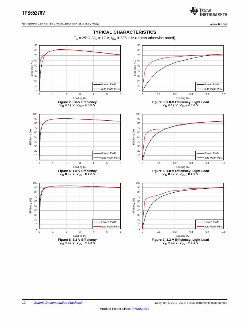
TYPICAL CHARACTERISTICSTA = 25°C, VIN = 12 V, fSW = 625 kHz (unless otherwise noted)
Figure 2. 0.8-V Efficiency Figure 3. 0.8-V Efficiency, Light LoadVIN = 12 V, VOUT = 0.8 V VIN = 12 V, VOUT = 0.8 V
Figure 4. 1.8-V Efficiency Figure 5. 1.8-V Efficiency, Light LoadVIN = 12 V, VOUT = 1.8 V VIN = 12 V, VOUT = 1.8 V
Figure 6. 3.3-V Efficiency Figure 7. 3.3-V Efficiency, Light LoadVIN = 12 V, VOUT = 3.3 V VIN = 12 V, VOUT = 3.3 V
12 Submit Documentation Feedback Copyright © 2013–2014, Texas Instruments Incorporated
Product Folder Links: TPS65276V

3.19
3.20
3.21
3.22
3.23
3.24
3.25
0 1 2 3 4 5 6
VO
UT (
V)
Loading (A)
Forced PWM
auto PWM-PSM
C012
4.75
4.80
4.85
4.90
4.95
0 1 2 3 4 5 6
VO
UT (
V)
Loading (A)
Forced PWM
auto PWM-PSM
C013
0.77
0.78
0.79
0.80
0.81
0 1 2 3 4 5 6
VO
UT (
V)
Loading (A)
Forced PWM
auto PWM-PSM
C010
1.76
1.77
1.78
1.79
1.80
1.81
0 1 2 3 4 5 6
VO
UT (
V)
Loading (A)
Forced PWM
auto PWM-PSM
C011
0
10
20
30
40
50
60
70
80
90
100
0 1 2 3 4 5 6
Effi
cien
cy (
%)
Loading (A)
Forced PWM
auto PWM-PSM
C008
0
10
20
30
40
50
60
70
80
90
100
0 0.1 0.2 0.3 0.4 0.5
Effi
cien
cy (
%)
Loading (A)
Forced PWM
auto PWM-PSM
C009
TPS65276V
www.ti.com SLVSBW0B –FEBRUARY 2013–REVISED JANUARY 2014
TYPICAL CHARACTERISTICS (continued)TA = 25°C, VIN = 12 V, fSW = 625 kHz (unless otherwise noted)
Figure 8. 5-V Efficiency Figure 9. 5-V Efficiency, Light LoadVIN = 12 V, VOUT = 5 V VIN = 12 V, VOUT = 5 V
Figure 10. 0.8-V Load Regulation Figure 11. 1.8-V Load RegulationVIN = 12 V, VOUT = 0.8 V VIN = 12 V, VOUT = 1.8 V
Figure 12. 3.3-V Load Regulation Figure 13. 5-V Load RegulationVIN = 12 V, VOUT = 3.3 V VIN = 12 V, VOUT = 5 V
Copyright © 2013–2014, Texas Instruments Incorporated Submit Documentation Feedback 13
Product Folder Links: TPS65276V
3.15
3.17
3.19
3.21
3.23
3.25
3.27
3.29
6 7 8 9 10 11 12 13 14 15 16 17 18
VO
UT (
V)
VIN (V)
forced PWM 0 A
forced PWM 4.5 A
auto PSM-PWM 0 A
C016
4.77
4.79
4.81
4.83
4.85
4.87
4.89
4.91
4.93
6 7 8 9 10 11 12 13 14 15 16 17 18
VO
UT (
V)
VIN (V)
forced PWM 0 A
forced PWM 4.5 A
auto PSM-PWM 0 A
C017
0.75
0.76
0.77
0.78
0.79
0.8
0.81
0.82
6 7 8 9 10 11 12 13 14 15 16 17 18
VO
UT (
V)
VIN (V)
forced PWM 0 A
forced PWM 4.5 A
auto PSM-PWM 0 A
C014
1.75
1.76
1.77
1.78
1.79
1.8
1.81
1.82
6 7 8 9 10 11 12 13 14 15 16 17 18
VO
UT (
V)
VIN (V)
forced PWM 0 A
forced PWM 4.5 A
auto PSM-PWM 0 A
C015
TPS65276V
SLVSBW0B –FEBRUARY 2013–REVISED JANUARY 2014 www.ti.com
TYPICAL CHARACTERISTICS (continued)TA = 25°C, VIN = 12 V, fSW = 625 kHz (unless otherwise noted)
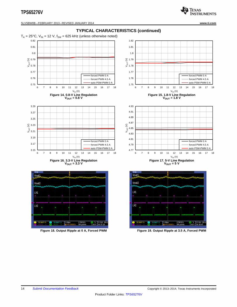
Figure 14. 0.8-V Line Regulation Figure 15. 1.8-V Line RegulationVOUT = 0.8 V VOUT = 1.8 V
Figure 16. 3.3-V Line Regulation Figure 17. 5-V Line RegulationVOUT = 3.3 V VOUT = 5 V
Figure 18. Output Ripple at 0 A, Forced PWM Figure 19. Output Ripple at 3.5 A, Forced PWM
14 Submit Documentation Feedback Copyright © 2013–2014, Texas Instruments Incorporated
Product Folder Links: TPS65276V

TPS65276V
www.ti.com SLVSBW0B –FEBRUARY 2013–REVISED JANUARY 2014
TYPICAL CHARACTERISTICS (continued)TA = 25°C, VIN = 12 V, fSW = 625 kHz (unless otherwise noted)
Figure 20. Output Ripple, Buck1 at 0.05 A, Figure 21. Startup With EnableBuck 2 at 0.2 A Auto PSM-PWM Mode
Figure 22. Shutdown With Enable Figure 23. Load Transient, Buck 1 2.5 A - 4.5 A,Buck2 0.5 A - 2.5 A
Figure 24. Load Transient, Buck 1 (0.5 A - 2.5 A) Figure 25. Load Transient, Buck 2 (0.5 A - 2.5 A)
Copyright © 2013–2014, Texas Instruments Incorporated Submit Documentation Feedback 15
Product Folder Links: TPS65276V
TPS65276V
SLVSBW0B –FEBRUARY 2013–REVISED JANUARY 2014 www.ti.com
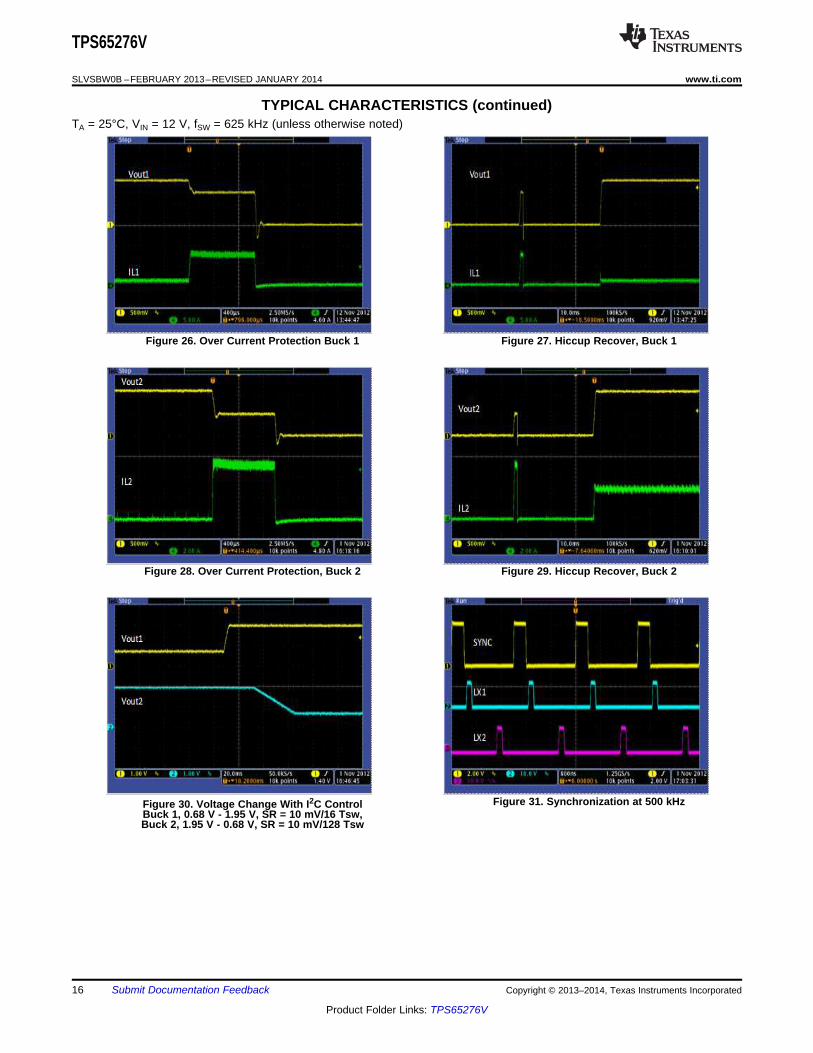
TYPICAL CHARACTERISTICS (continued)TA = 25°C, VIN = 12 V, fSW = 625 kHz (unless otherwise noted)
Figure 26. Over Current Protection Buck 1 Figure 27. Hiccup Recover, Buck 1
Figure 28. Over Current Protection, Buck 2 Figure 29. Hiccup Recover, Buck 2
Figure 31. Synchronization at 500 kHzFigure 30. Voltage Change With I2C ControlBuck 1, 0.68 V - 1.95 V, SR = 10 mV/16 Tsw,Buck 2, 1.95 V - 0.68 V, SR = 10 mV/128 Tsw
16 Submit Documentation Feedback Copyright © 2013–2014, Texas Instruments Incorporated
Product Folder Links: TPS65276V

TPS65276V
www.ti.com SLVSBW0B –FEBRUARY 2013–REVISED JANUARY 2014
OVERVIEW
TPS65276V is a dual 6.3-A/3.5-A output current, synchronous step-down (buck) converter with integratedn-channel MOSFETs. A wide 4.5-V to 18-V input supply range to buck encompasses most intermediate busvoltages operating off 9-V, 12-V or 15-V power bus.
TPS65276V is equipped with I2C compatible bus for sophisticated control and communication with SoC. With I2Cinterface, SoC can enable or disable the power converters, set output voltage and read status registers. Thebuck regulator has external feedback resistors that can be used for setting the initial start up voltage. Thefeedback voltage reference for this start-up option is 0.6V. Once the voltage identification VID DAC is updatedvia the I2C, output voltage of each channel can be independently programmed with 7 bits VID from 0.68 V to1.95 V in 10-mV steps. Output voltage transitions begin once the I2C interface receives the command for GO bitin command registers. In light loading condition, low pulse skipping mode can be I2C controlled or selected withMODE pin configuration.
TPS65276V implements a constant frequency, peak current mode control which simplifies external frequencycompensation. The wide switching frequency of 200 kHz to 1600 kHz allows for efficiency and size optimizationwhen selecting the output filter components. The switching frequency can be adjusted with an external resistor toground on the ROSC pin. The TPS65276V also has an internal phase lock loop (PLL) controlled by the ROSCpin that can be used to synchronize the switching cycle to the falling edge of an external system clock. 180° out-of-phase operation between two channels reduces input filter and power supply induced noise.
TPS65276V has been designed for safe monotonic startup into pre-biased loads. The default start up is whenVIN is typically 4.5 V. The EN pin has an internal pull-up current source that can be used to adjust the inputvoltage under voltage lockout (UVLO) with two external resistors. In addition, the EN pin can be floating forautomatically starting up the TPS65276V with the internal pull up current.
The integrated MOSFETs of each channel allow for high efficiency power supply designs with continuous outputcurrents up to 6 A and 3.5 A respectively. The MOSFETs have been sized to optimize efficiency for lower dutycycle applications.
The TPS65276V reduces the external component count by integrating the boot recharge circuit. The bias voltagefor the integrated high-side MOSFET is supplied by a capacitor between the BOOT and LX pins. The bootcapacitor voltage is monitored by a BOOT to LX UVLO (BOOT-LX UVLO) circuit allowing LX pin to be pulled lowto recharge the boot capacitor. The TPS65276V can operate at 100% duty cycle as long as the boot capacitorvoltage is higher than the preset BOOT-LX UVLO threshold which is typically 2.1 V.
The TPS65276V has a power good comparator (PWRGD) with hysteresis which monitors the output voltagethrough internal feedback voltage. I2C can read the power good status with commanding register.
The SS (soft start/tracking) pin is used to minimize inrush currents or provide power supply sequencing duringpower up. A small value capacitor or resistor divider should be coupled to the pin for soft start or critical powersupply sequencing requirements.
The TPS65276V is protected from output overvoltage, overload and thermal fault conditions. The TPS65276Vminimizes excessive output overvoltage transients by taking advantage of the power good comparator. When theovervoltage comparator is activated, the high-side MOSFET is turned off and prevented from turning on until theinternal feedback voltage is lower than 108% of the 0.6-V reference voltage. The TPS65276V implements bothhigh-side MOSFET overload protection and bidirectional low-side MOSFET overload protections which helpcontrol the inductor current and avoid current runaway. If the over current condition has lasted for more than thehiccup wait time, the TPS65276V will shut down and re-start after the hiccup time. The TPS65276V also shutsdown if the junction temperature is higher than thermal shutdown trip point. When the junction temperature drops20°C typically below the thermal shutdown trip point, the built-in thermal shutdown hiccup timer is triggered. TheTPS65276V will be restarted under control of the soft start circuit automatically after the thermal shutdown hiccuptime is over.
Furthermore, if the over-current condition has lasted for more than the hiccup wait time which is programmed for512 switching cycles, the TPS65276V will shut down itself and re-start after the hiccup time which is set for16384 cycles. The hiccup mode helps to reduce the device power dissipation under severe over-currentconditions.
The TPS65276V operates at any load conditions unless the COMP pin voltage drops below the COMP pin startswitching threshold which is typically 0.25 V.
Copyright © 2013–2014, Texas Instruments Incorporated Submit Documentation Feedback 17
Product Folder Links: TPS65276V

TPS65276V
SLVSBW0B –FEBRUARY 2013–REVISED JANUARY 2014 www.ti.com
When PSM mode operation is enabled, the TPS65276V monitors the peak switch current of the high-sideMOSFET. Once the peak switch current is lower than typically 1 A, the device stops switching to boost theefficiency until the peak switch current is higher than typically 1 A again.
18 Submit Documentation Feedback Copyright © 2013–2014, Texas Instruments Incorporated
Product Folder Links: TPS65276V
0.62 1
0.6
æ ö= ×ç ÷
-è øOUT
VR R
V V
IC
Vo
FB
R1
R20.6V
TPS65276V
www.ti.com SLVSBW0B –FEBRUARY 2013–REVISED JANUARY 2014
DETAILED DESCRIPTION
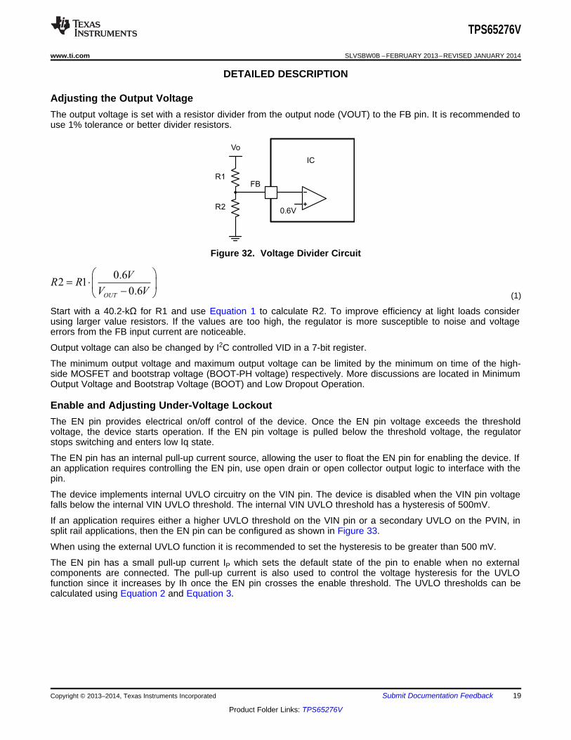
Adjusting the Output VoltageThe output voltage is set with a resistor divider from the output node (VOUT) to the FB pin. It is recommended touse 1% tolerance or better divider resistors.
Figure 32. Voltage Divider Circuit
(1)
Start with a 40.2-kΩ for R1 and use Equation 1 to calculate R2. To improve efficiency at light loads considerusing larger value resistors. If the values are too high, the regulator is more susceptible to noise and voltageerrors from the FB input current are noticeable.
Output voltage can also be changed by I2C controlled VID in a 7-bit register.
The minimum output voltage and maximum output voltage can be limited by the minimum on time of the high-side MOSFET and bootstrap voltage (BOOT-PH voltage) respectively. More discussions are located in MinimumOutput Voltage and Bootstrap Voltage (BOOT) and Low Dropout Operation.
Enable and Adjusting Under-Voltage LockoutThe EN pin provides electrical on/off control of the device. Once the EN pin voltage exceeds the thresholdvoltage, the device starts operation. If the EN pin voltage is pulled below the threshold voltage, the regulatorstops switching and enters low Iq state.
The EN pin has an internal pull-up current source, allowing the user to float the EN pin for enabling the device. Ifan application requires controlling the EN pin, use open drain or open collector output logic to interface with thepin.
The device implements internal UVLO circuitry on the VIN pin. The device is disabled when the VIN pin voltagefalls below the internal VIN UVLO threshold. The internal VIN UVLO threshold has a hysteresis of 500mV.
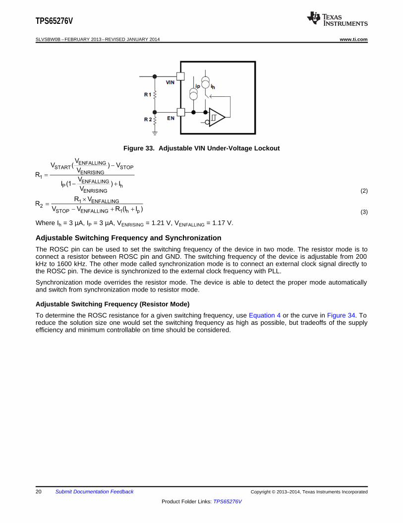
If an application requires either a higher UVLO threshold on the VIN pin or a secondary UVLO on the PVIN, insplit rail applications, then the EN pin can be configured as shown in Figure 33.
When using the external UVLO function it is recommended to set the hysteresis to be greater than 500 mV.
The EN pin has a small pull-up current IP which sets the default state of the pin to enable when no externalcomponents are connected. The pull-up current is also used to control the voltage hysteresis for the UVLOfunction since it increases by Ih once the EN pin crosses the enable threshold. The UVLO thresholds can becalculated using Equation 2 and Equation 3.
Copyright © 2013–2014, Texas Instruments Incorporated Submit Documentation Feedback 19
Product Folder Links: TPS65276V
1 ENFALLING2
STOP ENFALLING 1 h p
R VR
V V R (I I )
´=
- + +
ENFALLINGSTART STOP
ENRISING1
ENFALLINGP h
ENRISING
VV ( ) V
VR
VI (1 ) I
V
-
=
- +
TPS65276V
SLVSBW0B –FEBRUARY 2013–REVISED JANUARY 2014 www.ti.com
Figure 33. Adjustable VIN Under-Voltage Lockout
(2)
(3)
Where Ih = 3 µA, IP = 3 µA, VENRISING = 1.21 V, VENFALLING = 1.17 V.
Adjustable Switching Frequency and SynchronizationThe ROSC pin can be used to set the switching frequency of the device in two mode. The resistor mode is toconnect a resistor between ROSC pin and GND. The switching frequency of the device is adjustable from 200kHz to 1600 kHz. The other mode called synchronization mode is to connect an external clock signal directly tothe ROSC pin. The device is synchronized to the external clock frequency with PLL.
Synchronization mode overrides the resistor mode. The device is able to detect the proper mode automaticallyand switch from synchronization mode to resistor mode.
Adjustable Switching Frequency (Resistor Mode)To determine the ROSC resistance for a given switching frequency, use Equation 4 or the curve in Figure 34. Toreduce the solution size one would set the switching frequency as high as possible, but tradeoffs of the supplyefficiency and minimum controllable on time should be considered.
20 Submit Documentation Feedback Copyright © 2013–2014, Texas Instruments Incorporated
Product Folder Links: TPS65276V

ROSC
ROSC
ICMode
Selection
1.019osc swR (k ) 45580 f (kHz)-W = ×
TPS65276V
www.ti.com SLVSBW0B –FEBRUARY 2013–REVISED JANUARY 2014
Figure 34. ROSC vs Switching Frequency
(4)
SynchronizationAn internal phase locked loop (PLL) has been implemented to allow synchronization between 200 kHz and 1600kHz, and to easily switch from Resistor mode to Synchronization mode.
To implement the synchronization feature, connect a square wave clock signal to the ROSC pin with a duty cyclebetween 20% to 80%. The clock signal amplitude must transition lower than 0.8 V and higher than 2 V. The startof the switching cycle is synchronized to the falling edge of ROSC pin.
In applications where both Resistor mode and Synchronization mode are needed, the device can be configuredas shown in Figure 35. Before the external clock is present, the device works in Resistor mode and the switchingfrequency is set by ROSC resistor. When the external clock is present, the Synchronization mode overrides theResistor mode. The first time the ROSC pin is pulled above the ROSC high threshold (2 V), the device switchesfrom the Resistor mode to the Synchronization mode and the ROSC pin becomes high impedance as the PLLstarts to lock onto the frequency of the external clock. It is not recommended to switch from the Synchronizationmode back to the Resistor mode because the internal switching frequency drops to 100 kHz first before returningto the switching frequency set by ROSC resistor.
Figure 35. Resistor Mode and Synchronization Mode
Copyright © 2013–2014, Texas Instruments Incorporated Submit Documentation Feedback 21
Product Folder Links: TPS65276V

0.6 VTss(ms) Css(nF)
6 A
æ ö×= × ç ÷
× mè ø
TPS65276V
SLVSBW0B –FEBRUARY 2013–REVISED JANUARY 2014 www.ti.com
Soft Start TimeThe start-up of buck output is controlled by the voltage on the respective SS pin. When the voltage on the SS pinis less than the internal 0.6-V reference, the TPS65276V regulates the internal feedback voltage to the voltageon the SS pin instead of 0.6 V. The SS pin can be used to program an external soft-start function or to allowoutput of buck to track another supply during start-up. The device has an internal pull-up current source of 6 µAthat charges an external soft-start capacitor to provide a linear ramping voltage at SS pin. The TPS65276Vregulates the internal feedback voltage according to the voltage on the SS pin, allowing VOUT to rise smoothlyfrom 0 V to its final regulated voltage. The total soft-start time will be calculated approximately:
(5)
VID ControlWhen I2C is not in function, the output voltage of TPS65276V is solely set by an external resistor divider. Ifsystem wants to control the output voltage, VID (voltage identification) DAC can be controlled via I2C interface tothe Output Voltage Selection register of 0x00H (Buck 1) and 0x1H (Buck 2). Output voltage is required to bepreset by the external resistor divider. When VID DAC is selected via I2C interface and the “GO” bit in commandregister is set, the output voltage is set with the internal voltage divider over the external voltage divider.
Out-of-Phase OperationIn order to reduce input ripple current, Buck 1 and Buck 2 operate 180° out-of-phase. This enables the systemhaving less input ripple, then to lower component cost, save board space and reduce EMI.
Output Overvoltage Protection (OVP)The device incorporates an output overvoltage protection (OVP) circuit to minimize output voltage overshoot. Forexample, when the power supply output is overloaded the error amplifier compares the actual output voltage tothe internal reference voltage. If the FB pin voltage is lower than the internal reference voltage for a considerabletime, the output of the error amplifier demands maximum output current. Once the condition is removed, theregulator output rises and the error amplifier output transitions to the steady state voltage. In some applicationswith small output capacitance, the power supply output voltage can respond faster than the error amplifier. Thisleads to the possibility of an output overshoot. The OVP feature minimizes the overshoot by comparing the FBpin voltage to the OVP threshold. If the FB pin voltage is greater than the OVP threshold the high-side MOSFETis turned off preventing current from flowing to the output and minimizing output overshoot. When the FB voltagedrops lower than the OVP threshold, the high-side MOSFET is allowed to turn on at the next clock cycle.
Bootsrap Voltage (BOOT) and Low Dropout OperationThe device has an integrated boot regulator, and requires a small ceramic capacitor between the BOOT and LXpins to provide the gate drive voltage for the high-side MOSFET. The boot capacitor is charged when the BOOTpin voltage is less than VIN and BOOT-LX voltage is below regulation. The value of this ceramic capacitor shouldbe 0.1 μF. A ceramic capacitor with an X7R or X5R grade dielectric with a voltage rating of 10 V or higher isrecommended because of the stable characteristics over temperature and voltage.
To improve drop out, the device is designed to operate at 100% duty cycle as long as the BOOT to LX pinvoltage is greater than the BOOT-LX UVLO threshold which is typically 2.1 V. When the voltage between BOOTand LX drops below the BOOT-LX UVLO threshold the high-side MOSFET is turned off and the low-sideMOSFET is turned on allowing the boot capacitor to be recharged. In applications with split input voltage rails.
100% duty cycle operation can be achieved as long as (VIN – PVIN) > 4 V.
Over Current ProtectionThe device is protected from over current conditions by cycle-by-cycle current limiting on both the high-sideMOSFET and the low-side MOSFET.
22 Submit Documentation Feedback Copyright © 2013–2014, Texas Instruments Incorporated
Product Folder Links: TPS65276V

TPS65276V
www.ti.com SLVSBW0B –FEBRUARY 2013–REVISED JANUARY 2014
High-Side MOSFET Over Current ProtectionThe device implements current mode control which uses the COMP pin voltage to control the turn off of the high-side MOSFET and the turn on of the low-side MOSFET on a cycle by cycle basis. Each cycle the switch currentand the current reference generated by the COMP pin voltage are compared, when the peak switch currentintersects the current reference the high-side switch is turned off.
Low-Side MOSFET Over Current ProtectionWhile the low-side MOSFET is turned on its conduction current is monitored by the internal circuitry. Duringnormal operation the low-side MOSFET sources current to the load. At the end of every clock cycle, the low-sideMOSFET sourcing current is compared to the internally set low-side sourcing current limit. If the low-sidesourcing current is exceeded, the high-side MOSFET is not turned on and the low-side MOSFET stays on for thenext cycle. The high-side MOSFET is turned on again when the low-side current is below the low-side sourcingcurrent limit at the start of a cycle.
The low-side MOSFET may also sink current from the load. If the low-side sinking current limit is exceeded thelow-side MOSFET is turned off immediately for the rest of that clock cycle. In this scenario both MOSFETs areoff until the start of the next cycle.
Furthermore, if an output overload condition (as measured by the COMP pin voltage) has lasted for more thanthe hiccup wait time which is programmed for 512 switching cycles, the device will shut down itself and restartafter the hiccup time of 16384 cycles. The hiccup mode helps to reduce the device power dissipation undersevere overcurrent conditions.
Thermal ShutdownThe internal thermal shutdown circuitry forces the device to stop switching if the junction temperature exceeds160°C typically. Once the junction temperature drops below 140°C typically, the internal thermal hiccup timer willstart to count. The device reinitiates the power up sequence after the built-in thermal shutdown hiccup time(16384 cycles) is over.
Copyright © 2013–2014, Texas Instruments Incorporated Submit Documentation Feedback 23
Product Folder Links: TPS65276V

outo
sw out
2 IC
f V
× D=
× D
rippleLpeak out
II I
2= +
2out inmax out
2 inmaxLrms O
V (V V )( )
V L fswI I
12
× -
× ×= +
inmax out outripple
inmax sw
V V VI
L V f
-= ×
×
inmax out out
o inmax sw
V V VL
I LIR V f
-= ×
× ×
TPS65276V
SLVSBW0B –FEBRUARY 2013–REVISED JANUARY 2014 www.ti.com
APPLICATION INFORMATION
Output Inductor SelectionTo calculate the value of the output inductor, use Equation 18. LIR is a coefficient that represents the amount ofinductor ripple current relative to the maximum output current. The inductor ripple current is filtered by the outputcapacitor. Therefore, choosing high inductor ripple currents impact the selection of the output capacitor since theoutput capacitor must have a ripple current rating equal to or greater than the inductor ripple current. In general,the inductor ripple value is at the discretion of the designer; however, LIR is normally from 0.1 to 0.3 for themajority of applications.
(6)
For the output filter inductor, it is important that the RMS current and saturation current ratings not be exceeded.The RMS and peak inductor current can be found from Equation 8 and Equation 9.
(7)
(8)
(9)
The current flowing through the inductor is the inductor ripple current plus the output current. During power up,faults or transient load conditions, the inductor current can increase above the calculated peak inductor currentlevel calculated above. In transient conditions, the inductor current can increase up to the switch current limit ofthe device. For this reason, the most conservative approach is to specify an inductor with a saturation currentrating equal to or greater than the switch current limit rather than the peak inductor current.
Output Capacitor SelectionThere are three primary considerations for selecting the value of the output capacitor. The output capacitordetermines the modulator pole, the output voltage ripple, and how the regulator responds to a large change inload current. The output capacitance needs to be selected based on the most stringent of these three criteria.
The desired response to a large change in the load current is the first criteria. The output capacitor needs tosupply the load with current when the regulator cannot. This situation would occur if there are desired hold-uptimes for the regulator where the output capacitor must hold the output voltage above a certain level for aspecified amount of time after the input power is removed. The regulator is also temporarily not able to supplysufficient output current if there is a large, fast increase in the current needs of the load such as a transition fromno load to full load. The regulator usually needs two or more clock cycles for the control loop to see the changein load current and output voltage and adjust the duty cycle to react to the change. The output capacitor must besized to supply the extra current to the load until the control loop responds to the load change. The outputcapacitance must be large enough to supply the difference in current for 2 clock cycles while only allowing atolerable amount of droop in the output voltage. Equation 10 shows the minimum output capacitance necessaryto accomplish this.
(10)
Where ΔIOUT is the change in output current, fSW is the regulators switching frequency and ΔVOUT is the allowablechange in the output voltage. For this example, the transient load response is specified as a 5% change in VOUTfor a load step of 3 A. For this example, ΔIOUT = 3 A and ΔVOUT = 0.05 x 3.3 = 0.165 V. Using these numbersgives a minimum capacitance of 75.8 μF. This value does not take the ESR of the output capacitor into accountin the output voltage change. For ceramic capacitors, the ESR is usually small enough to ignore in thiscalculation.
24 Submit Documentation Feedback Copyright © 2013–2014, Texas Instruments Incorporated
Product Folder Links: TPS65276V
outmaxin
in sw
I 0.25V
C f
×D =
×
( )inmin outoutinrms out
inmin inmin
V VVI I
V V
-= × ×
out inmax outcorms
inmax sw
V (V V )I
12 V L f
× -=
× × ×
orippleesr
oripple
VR
I<
ooripplesw
oripple
1 1C
V8 f
I
> ××
TPS65276V
www.ti.com SLVSBW0B –FEBRUARY 2013–REVISED JANUARY 2014
Equation 11 calculates the minimum output capacitance needed to meet the output voltage ripple specification.Where fSW is the switching frequency, Voripple is the maximum allowable output voltage ripple, and Ioripple is theinductor ripple current.
(11)
Equation 12 calculates the maximum ESR an output capacitor can have to meet the output voltage ripplespecification.
(12)
Additional capacitance de-ratings for aging, temperature and DC bias should be factored in which increases thisminimum value.
Capacitors generally have limits to the amount of ripple current they can handle without failing or producingexcess heat. An output capacitor that can support the inductor ripple current must be specified. Some capacitordata sheets specify the root mean square (RMS) value of the maximum ripple current. Equation 13 can be usedto calculate the RMS ripple current the output capacitor needs to support.
(13)
Input Capacitor SelectionThe TPS65276V requires a high quality ceramic, type X5R or X7R, input decoupling capacitor of at least 10-µFof effective capacitance on the PVIN input voltage pins. In some applications additional bulk capacitance mayalso be required for the PVIN input. The effective capacitance includes any DC bias effects. The voltage rating ofthe input capacitor must be greater than the maximum input voltage. The capacitor must also have a ripplecurrent rating greater than the maximum input current ripple of the TPS65276V. The input ripple current can becalculated using Equation 14.
(14)
The value of a ceramic capacitor varies significantly over temperature and the amount of DC bias applied to thecapacitor. The capacitance variations due to temperature can be minimized by selecting a dielectric material thatis stable over temperature. X5R and X7R ceramic dielectrics are usually selected for power regulator capacitorsbecause they have a high capacitance to volume ratio and are fairly stable over temperature. The outputcapacitor must also be selected with the DC bias taken into account. The capacitance value of a capacitordecreases as the DC bias across a capacitor increases. For this example design, a ceramic capacitor with atleast a 25-V voltage rating is required to support the maximum input voltage. TPS65276V may operate from asingle supply. The input capacitance value determines the input ripple voltage of the regulator. The input voltageripple can be calculated using Equation 15.
(15)
Copyright © 2013–2014, Texas Instruments Incorporated Submit Documentation Feedback 25
Product Folder Links: TPS65276V

Current Sense
I/V Converter
VVref 6.0
Li ESRR
1R
2R
cR
oC
cC
bC
LR
µsgM 1350
COMPVFB
EA
1C
VOUT
VAgmps /10=
==
ESRb
C
R CoC
R
×=
LC
C
R CoC
R
×=
O L
1(fp ) s
C R 2= ×
× × p
2
C
M ps
fc Vo CoR
g Vref gm
p × × ×
=
× ×
TPS65276V
SLVSBW0B –FEBRUARY 2013–REVISED JANUARY 2014 www.ti.com
Loop CompensationIntegrated buck DC/DC converter in TPS65276V incorporates a peak current mode control scheme. The erroramplifier is a transconductance amplifier with a gain of 1350 µA/V. A typical type II compensation circuitadequately delivers a phase margin between 60° and 90°. Cb adds a high frequency pole to attenuate highfrequency noise when needed. To calculate the external compensation components, follow the following steps.1. Select switching frequency fsw that is appropriate for application depending on L and C sizes, output ripple,
EMI, and etc. Switching frequency between 500 kHz to 1 MHz gives best trade off between performance andcost. To optimize efficiency, lower switching frequency is desired.
2. Set up cross over frequency, fc, which is typically between 1/5 and 1/20 of fsw.3. RC can be determined by:
Where is the error amplifier gain (1350 µA/V) is the power stage voltage to current conversion gain (10 A/V).4. Calculate CC by placing a compensation zero at or before the dominant pole:
(16)
(17)5. Optional Cb can be used to cancel the zero from the ESR associated with CO.
(18)
Figure 36. DC/DC Loop Compensation
26 Submit Documentation Feedback Copyright © 2013–2014, Texas Instruments Incorporated
Product Folder Links: TPS65276V
TPS65276V
www.ti.com SLVSBW0B –FEBRUARY 2013–REVISED JANUARY 2014
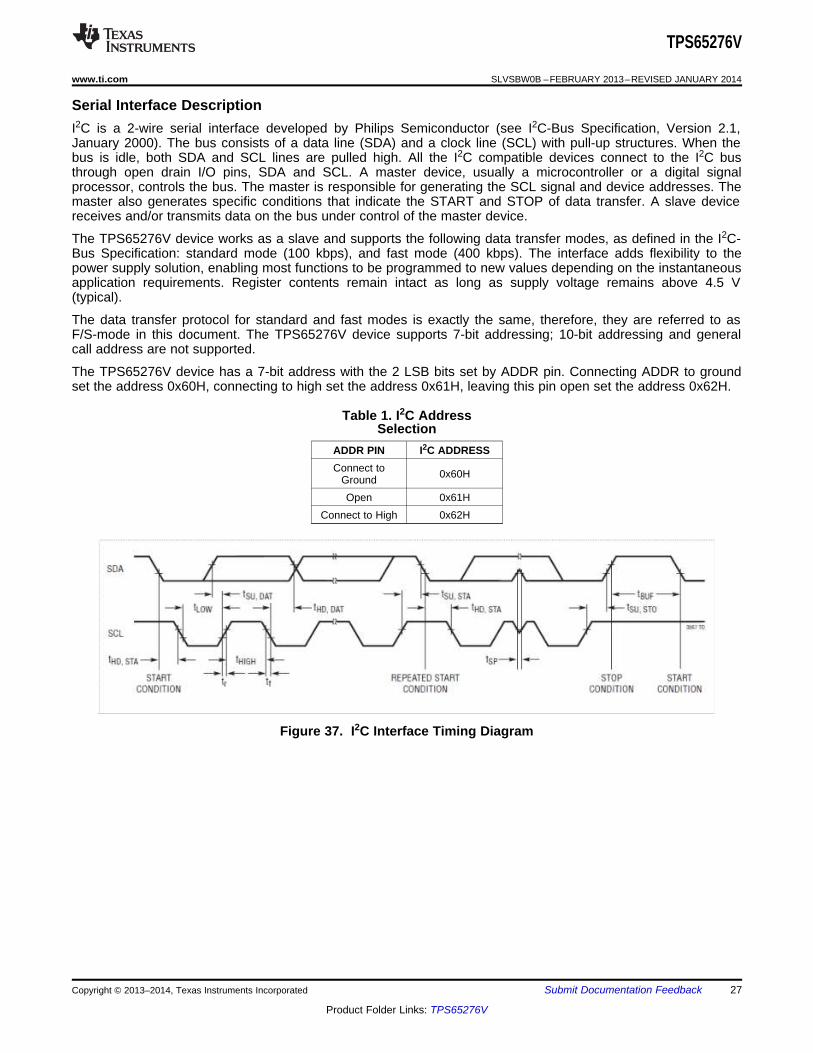
Serial Interface DescriptionI2C is a 2-wire serial interface developed by Philips Semiconductor (see I2C-Bus Specification, Version 2.1,January 2000). The bus consists of a data line (SDA) and a clock line (SCL) with pull-up structures. When thebus is idle, both SDA and SCL lines are pulled high. All the I2C compatible devices connect to the I2C busthrough open drain I/O pins, SDA and SCL. A master device, usually a microcontroller or a digital signalprocessor, controls the bus. The master is responsible for generating the SCL signal and device addresses. Themaster also generates specific conditions that indicate the START and STOP of data transfer. A slave devicereceives and/or transmits data on the bus under control of the master device.
The TPS65276V device works as a slave and supports the following data transfer modes, as defined in the I2C-Bus Specification: standard mode (100 kbps), and fast mode (400 kbps). The interface adds flexibility to thepower supply solution, enabling most functions to be programmed to new values depending on the instantaneousapplication requirements. Register contents remain intact as long as supply voltage remains above 4.5 V(typical).
The data transfer protocol for standard and fast modes is exactly the same, therefore, they are referred to asF/S-mode in this document. The TPS65276V device supports 7-bit addressing; 10-bit addressing and generalcall address are not supported.
The TPS65276V device has a 7-bit address with the 2 LSB bits set by ADDR pin. Connecting ADDR to groundset the address 0x60H, connecting to high set the address 0x61H, leaving this pin open set the address 0x62H.
Table 1. I2C AddressSelection
ADDR PIN I2C ADDRESSConnect to 0x60HGround
Open 0x61HConnect to High 0x62H
Figure 37. I2C Interface Timing Diagram
Copyright © 2013–2014, Texas Instruments Incorporated Submit Documentation Feedback 27
Product Folder Links: TPS65276V
N: Not Acknowledge
A: Acknowledge
S: Start
P: Stop
Sr: Repeated Start
System Host
Chip
S 7-Bit Slave Address 0 A Register1 Address A Sr 17-Bit Slave Address A
Data Byte N P
S 7-Bit Slave Address 0 A Register Address A Data Byte A P
TPS65276V
SLVSBW0B –FEBRUARY 2013–REVISED JANUARY 2014 www.ti.com
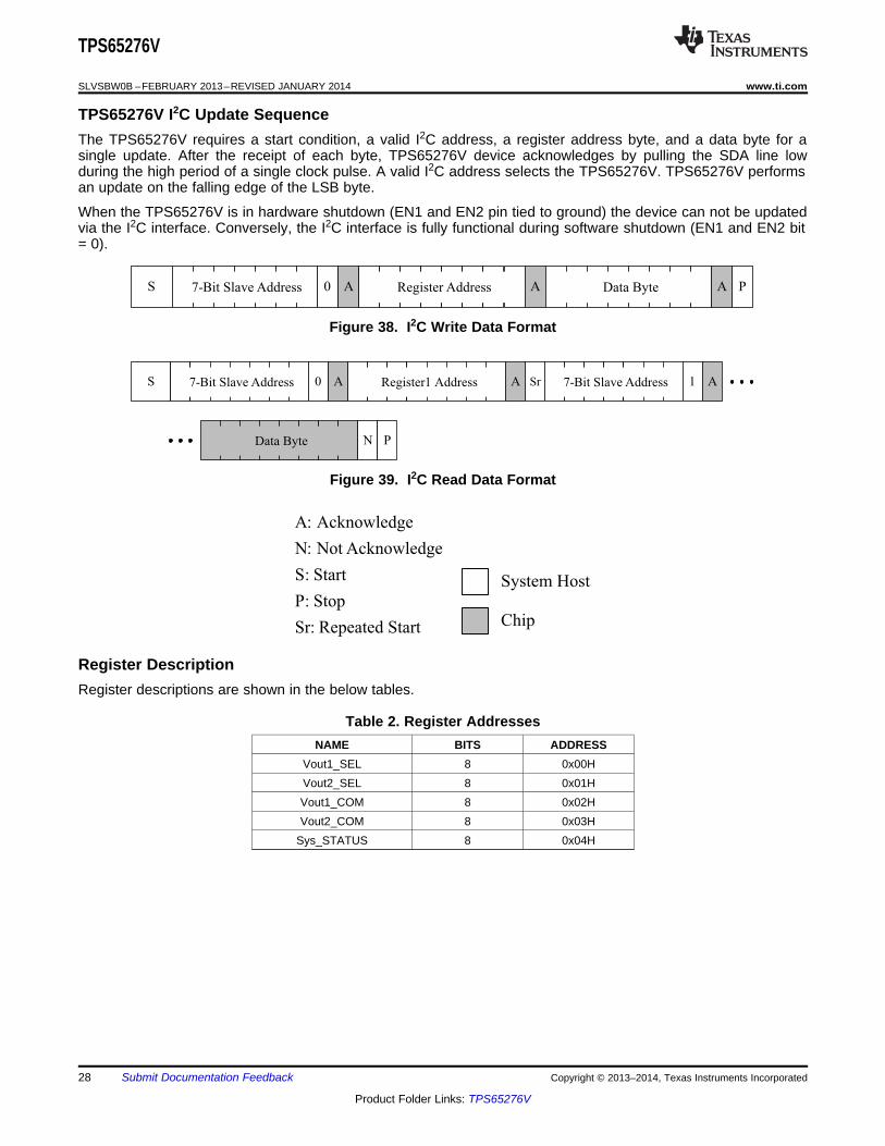
TPS65276V I2C Update SequenceThe TPS65276V requires a start condition, a valid I2C address, a register address byte, and a data byte for asingle update. After the receipt of each byte, TPS65276V device acknowledges by pulling the SDA line lowduring the high period of a single clock pulse. A valid I2C address selects the TPS65276V. TPS65276V performsan update on the falling edge of the LSB byte.
When the TPS65276V is in hardware shutdown (EN1 and EN2 pin tied to ground) the device can not be updatedvia the I2C interface. Conversely, the I2C interface is fully functional during software shutdown (EN1 and EN2 bit= 0).
Figure 38. I2C Write Data Format
Figure 39. I2C Read Data Format
Register DescriptionRegister descriptions are shown in the below tables.
Table 2. Register AddressesNAME BITS ADDRESS
Vout1_SEL 8 0x00HVout2_SEL 8 0x01HVout1_COM 8 0x02HVout2_COM 8 0x03H
Sys_STATUS 8 0x04H
28 Submit Documentation Feedback Copyright © 2013–2014, Texas Instruments Incorporated
Product Folder Links: TPS65276V

TPS65276V
www.ti.com SLVSBW0B –FEBRUARY 2013–REVISED JANUARY 2014
Table 3. Vout1 Voltage Selection RegisterNUMBER OF BITS ACCESS NAME DEFAULT VALUE DESCRIPTION
Vout1_SEL 7 10-mV step, from 0.68 V to 1.95 V
Go bit, must set “1” to enable I2C voltageaddress: 0x00H Bit 7 R/W Vout1_Bit7 0 control
Bit 6 R/W Vout1_Bit6 0
Bit 5 R/W Vout1_Bit5 0
Bit 4 R/W Vout1_Bit4 0
Bit 3 R/W Vout1_Bit3 0 0x00H: 0.68V; 0x7FH: 1.95V
Bit 2 R/W Vout1_Bit2 0
Bit 1 R/W Vout1_Bit1 0
Bit 0 R/W Vout1_Bit0 0
Table 4. Vout2 Voltage Selection RegisterNUMBER OF BITS ACCESS NAME DEFAULT VALUE DESCRIPTION
Vout2_SEL 7 10-mV step, from 0.68 V to 1.95 V
Go bit, must set “1” to enable I2C voltageaddress: 0x01H Bit 7 R/W Vout2_Bit7 0 control
Bit 6 R/W Vout2_Bit6 0
Bit 5 R/W Vout2_Bit5 0
Bit 4 R/W Vout2_Bit4 0
Bit 3 R/W Vout2_Bit3 0 0x00H: 0.68V; 0x7FH: 1.95V
Bit 2 R/W Vout2_Bit2 0
Bit 1 R/W Vout2_Bit1 0
Bit 0 R/W Vout2_Bit0 0
Table 5. Vout1 Command RegisterNUMBER OF BITS ACCESS NAME DEFAULT VALUE DESCRIPTION
Vout1_COM 8
address: 0x02H Bit 7 Reserved
Bit 6 R/W Slew Rate 3 0 Vout slew rate control.000: 10 mV/cycle;Bit 5 R/W Slew Rate 2 0 001: 10 mV/2 cycles;010: 10 mV/4 cycles;011: 10 mV/8 cycles;100: 10 mV/16cycles;Bit 4 R/W Slew Rate 1 0 101: 10 mV/32cycles;110: 10 mV/64cycles;111: 10 mV/128 cycles
Bit 3 Reserved
Bit 2 R/W PSM Mode 0 00: select by MODE pin;01: forced PWM mode;10: auto PSM-PWM mode;Bit 1 R/W PSM Mode 011: reserved
0: output enabled;Bit 0 R/W Disable1 0 1: output disabled
Copyright © 2013–2014, Texas Instruments Incorporated Submit Documentation Feedback 29
Product Folder Links: TPS65276V
TPS65276V
SLVSBW0B –FEBRUARY 2013–REVISED JANUARY 2014 www.ti.com
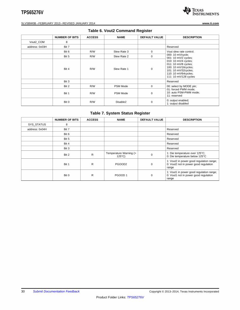
Table 6. Vout2 Command RegisterNUMBER OF BITS ACCESS NAME DEFAULT VALUE DESCRIPTION
Vout2_COM 8
address: 0x03H Bit 7 Reserved
Bit 6 R/W Slew Rate 3 0 Vout slew rate control.000: 10 mV/cycle;Bit 5 R/W Slew Rate 2 0 001: 10 mV/2 cycles;010: 10 mV/4 cycles;011: 10 mV/8 cycles;100: 10 mV/16cycles;Bit 4 R/W Slew Rate 1 0 101: 10 mV/32cycles;110: 10 mV/64cycles;111: 10 mV/128 cycles
Bit 3 Reserved
Bit 2 R/W PSM Mode 0 00: select by MODE pin;01: forced PWM mode;10: auto PSM-PWM mode;Bit 1 R/W PSM Mode 011: reserved
0: output enabled;Bit 0 R/W Disable2 0 1: output disabled
Table 7. System Status RegisterNUMBER OF BITS ACCESS NAME DEFAULT VALUE DESCRIPTION
SYS_STATUS 8
address: 0x04H Bit 7 Reserved
Bit 6 Reserved
Bit 5 Reserved
Bit 4 Reserved
Bit 3 Reserved
Temperature Warning (> 1: Die temperature over 125°C;Bit 2 R 0125°C) 0: Die temperature below 125°C
1: Vout2 in power good regulation range;Bit 1 R PGOOD2 0 0: Vout2 not in power good regulation
range
1: Vout1 in power good regulation range;Bit 0 R PGOOD 1 0 0: Vout1 not in power good regulation
range
30 Submit Documentation Feedback Copyright © 2013–2014, Texas Instruments Incorporated
Product Folder Links: TPS65276V

TPS65276V
www.ti.com SLVSBW0B –FEBRUARY 2013–REVISED JANUARY 2014
Table 8. Vout1 and Vout2 Output Voltage SettingVOUT_SEL OUTPUT VOUT_SEL OUTPUT VOUT_SEL OUTPUT VOUT_SEL OUTPUT
<7:0> VOLTAGE (V) <7:0> VOLTAGE (V) <7:0> VOLTAGE (V) <7:0> VOLTAGE (V)
0 0.68 20 1 40 1.32 60 1.64
1 0.69 21 1.01 41 1.33 61 1.65
2 0.7 22 1.02 42 1.34 62 1.66
3 0.71 23 1.03 43 1.35 63 1.67
4 0.72 24 1.04 44 1.36 64 1.68
5 0.73 25 1.05 45 1.37 65 1.69
6 0.74 26 1.06 46 1.38 66 1.7
7 0.75 27 1.07 47 1.39 67 1.71
8 0.76 28 1.08 48 1.4 68 1.72
9 0.77 29 1.09 49 1.41 69 1.73
A 0.78 2A 1.1 4A 1.42 6A 1.74
B 0.79 2B 1.11 4B 1.43 6B 1.75
C 0.8 2C 1.12 4C 1.44 6C 1.76
D 0.81 2D 1.13 4D 1.45 6D 1.77
E 0.82 2E 1.14 4E 1.46 6E 1.78
F 0.83 2F 1.15 4F 1.47 6F 1.79
10 0.84 30 1.16 50 1.48 70 1.8
11 0.85 31 1.17 51 1.49 71 1.81
12 0.86 32 1.18 52 1.5 72 1.82
13 0.87 33 1.19 53 1.51 73 1.83
14 0.88 34 1.2 54 1.52 74 1.84
15 0.89 35 1.21 55 1.53 75 1.85
16 0.9 36 1.22 56 1.54 76 1.86
17 0.91 37 1.23 57 1.55 77 1.87
18 0.92 38 1.24 58 1.56 78 1.88
19 0.93 39 1.25 59 1.57 79 1.89
1A 0.94 3A 1.26 5A 1.58 7A 1.9
1B 0.95 3B 1.27 5B 1.59 7B 1.91
1C 0.96 3C 1.28 5C 1.6 7C 1.92
1D 0.97 3D 1.29 5D 1.61 7D 1.93
1E 0.98 3E 1.3 5E 1.62 7E 1.94
1F 0.99 3F 1.31 5F 1.63 7F 1.95
Copyright © 2013–2014, Texas Instruments Incorporated Submit Documentation Feedback 31
Product Folder Links: TPS65276V

PGND
PGND
PGND
PGND
AGND
LX2
LX2
LX1
LX1
V7V
G
G
PGND
PGND 2
1
PGND
PGND
V7V
VIN2
VIN1
PGND
VOUT2
VOUT1
PGND
PGND
EN1
EN2
SDA
SCL
DVCC
LX1
LX1
LX2
LX2
PGND
AGND
TPS65276V
SLVSBW0B –FEBRUARY 2013–REVISED JANUARY 2014 www.ti.com
PCB Layout GuidelineTPS65276V can be layout on 2-layer PCB illustrated below.
Layout is a critical portion of good power supply design. See Figure 40 for a PCB layout example. The top layercontains the main power traces for VIN, VOUT, and VLX. Also on the top layer are connections for the remainingpins of the TPS65276V and a large top side area filled with ground. The top layer ground area should beconnected to the internal ground layer(s) using vias at the input bypass capacitor, the output filter capacitor anddirectly under the TPS65276V device to provide a thermal path from the exposed thermal pad land to ground.The bottom layer acts as ground plane connecting analog ground and power ground.
The GND pin should be tied directly to the power pad under the IC and the power pad. For operation at full ratedload, the top side ground area together with the internal ground plane, must provide adequate heat dissipatingarea. There are several signals paths that conduct fast changing currents or voltages that can interact with strayinductance or parasitic capacitance to generate noise or degrade the power supplies performance. To helpeliminate these problems, the PVIN pin should be bypassed to ground with a low ESR ceramic bypass capacitorwith X5R or X7R dielectric. Care should be taken to minimize the loop area formed by the bypass capacitorconnections, the PVIN pins, and the ground connections.
The VIN pin must also be bypassed to ground using a low ESR ceramic capacitor with X5R or X7R dielectric.
Since the LX connection is the switching node, the output inductor should be located close to the LX pins, andthe area of the PCB conductor minimized to prevent excessive capacitive coupling. The output filter capacitorground should use the same power ground trace as the PVIN input bypass capacitor. Try to minimize thisconductor length while maintaining adequate width. The additional external components can be placedapproximately as shown.
Figure 40. TPS65276V Layout on 2-layer PCB
32 Submit Documentation Feedback Copyright © 2013–2014, Texas Instruments Incorporated
Product Folder Links: TPS65276V
TPS65276V
www.ti.com SLVSBW0B –FEBRUARY 2013–REVISED JANUARY 2014
REVISION HISTORY
Changes from Revision A (June 2013) to Revision B Page
• Changed FUNCTIONAL BLOCK DIAGRAM ........................................................................................................................ 4• Changed ABSOLUTE MAXIMUM RATINGS table ............................................................................................................... 8
Copyright © 2013–2014, Texas Instruments Incorporated Submit Documentation Feedback 33
Product Folder Links: TPS65276V
PACKAGE OPTION ADDENDUM
www.ti.com 10-Dec-2020
Addendum-Page 1
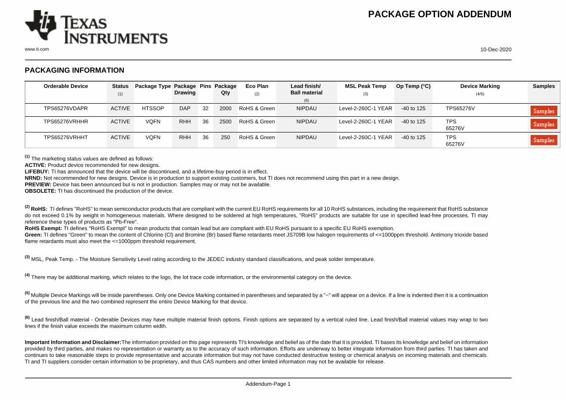
PACKAGING INFORMATION
Orderable Device Status(1)
Package Type PackageDrawing
Pins PackageQty
Eco Plan(2)
Lead finish/Ball material
(6)
MSL Peak Temp(3)
Op Temp (°C) Device Marking(4/5)
Samples
TPS65276VDAPR ACTIVE HTSSOP DAP 32 2000 RoHS & Green NIPDAU Level-2-260C-1 YEAR -40 to 125 TPS65276V
TPS65276VRHHR ACTIVE VQFN RHH 36 2500 RoHS & Green NIPDAU Level-2-260C-1 YEAR -40 to 125 TPS65276V
TPS65276VRHHT ACTIVE VQFN RHH 36 250 RoHS & Green NIPDAU Level-2-260C-1 YEAR -40 to 125 TPS65276V
(1) The marketing status values are defined as follows:ACTIVE: Product device recommended for new designs.LIFEBUY: TI has announced that the device will be discontinued, and a lifetime-buy period is in effect.NRND: Not recommended for new designs. Device is in production to support existing customers, but TI does not recommend using this part in a new design.PREVIEW: Device has been announced but is not in production. Samples may or may not be available.OBSOLETE: TI has discontinued the production of the device.
(2) RoHS: TI defines "RoHS" to mean semiconductor products that are compliant with the current EU RoHS requirements for all 10 RoHS substances, including the requirement that RoHS substancedo not exceed 0.1% by weight in homogeneous materials. Where designed to be soldered at high temperatures, "RoHS" products are suitable for use in specified lead-free processes. TI mayreference these types of products as "Pb-Free".RoHS Exempt: TI defines "RoHS Exempt" to mean products that contain lead but are compliant with EU RoHS pursuant to a specific EU RoHS exemption.Green: TI defines "Green" to mean the content of Chlorine (Cl) and Bromine (Br) based flame retardants meet JS709B low halogen requirements of <=1000ppm threshold. Antimony trioxide basedflame retardants must also meet the <=1000ppm threshold requirement.
(3) MSL, Peak Temp. - The Moisture Sensitivity Level rating according to the JEDEC industry standard classifications, and peak solder temperature.
(4) There may be additional marking, which relates to the logo, the lot trace code information, or the environmental category on the device.
(5) Multiple Device Markings will be inside parentheses. Only one Device Marking contained in parentheses and separated by a "~" will appear on a device. If a line is indented then it is a continuationof the previous line and the two combined represent the entire Device Marking for that device.
(6) Lead finish/Ball material - Orderable Devices may have multiple material finish options. Finish options are separated by a vertical ruled line. Lead finish/Ball material values may wrap to twolines if the finish value exceeds the maximum column width.
Important Information and Disclaimer:The information provided on this page represents TI's knowledge and belief as of the date that it is provided. TI bases its knowledge and belief on informationprovided by third parties, and makes no representation or warranty as to the accuracy of such information. Efforts are underway to better integrate information from third parties. TI has taken andcontinues to take reasonable steps to provide representative and accurate information but may not have conducted destructive testing or chemical analysis on incoming materials and chemicals.TI and TI suppliers consider certain information to be proprietary, and thus CAS numbers and other limited information may not be available for release.

PACKAGE OPTION ADDENDUM
www.ti.com 10-Dec-2020
Addendum-Page 2
In no event shall TI's liability arising out of such information exceed the total purchase price of the TI part(s) at issue in this document sold by TI to Customer on an annual basis.
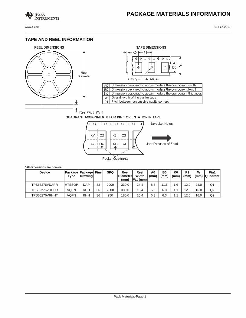
TAPE AND REEL INFORMATION
*All dimensions are nominal
Device PackageType
PackageDrawing
Pins SPQ ReelDiameter
(mm)
ReelWidth
W1 (mm)
A0(mm)
B0(mm)
K0(mm)
P1(mm)
W(mm)
Pin1Quadrant
TPS65276VDAPR HTSSOP DAP 32 2000 330.0 24.4 8.6 11.5 1.6 12.0 24.0 Q1
TPS65276VRHHR VQFN RHH 36 2500 330.0 16.4 6.3 6.3 1.1 12.0 16.0 Q2
TPS65276VRHHT VQFN RHH 36 250 180.0 16.4 6.3 6.3 1.1 12.0 16.0 Q2
PACKAGE MATERIALS INFORMATION
www.ti.com 15-Feb-2019
Pack Materials-Page 1
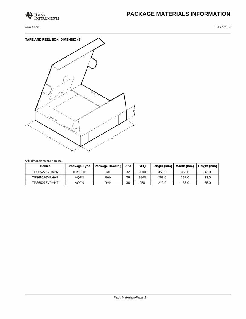
*All dimensions are nominal
Device Package Type Package Drawing Pins SPQ Length (mm) Width (mm) Height (mm)
TPS65276VDAPR HTSSOP DAP 32 2000 350.0 350.0 43.0
TPS65276VRHHR VQFN RHH 36 2500 367.0 367.0 38.0
TPS65276VRHHT VQFN RHH 36 250 210.0 185.0 35.0
PACKAGE MATERIALS INFORMATION
www.ti.com 15-Feb-2019
Pack Materials-Page 2

www.ti.com
GENERIC PACKAGE VIEW
This image is a representation of the package family, actual package may vary.Refer to the product data sheet for package details.
VQFN - 1 mm max heightRHH 36PLASTIC QUAD FLATPACK - NO LEAD6 x 6, 0.5 mm pitch
4225440/A

www.ti.com
PACKAGE OUTLINE
6.15.9
6.15.9
1.00.8
0.050.00
2X 4
32X 0.5
2X 4
36X 0.650.45
36X 0.300.18
4.1 0.1
(0.2) TYP
VQFN - 1 mm max heightRHH0036BPLASTIC QUAD FLATPACK - NO LEAD
4225414/A 10/2019
0.08 C
0.1 C A B0.05
NOTES: 1. All linear dimensions are in millimeters. Any dimensions in parenthesis are for reference only. Dimensioning and tolerancing per ASME Y14.5M. 2. This drawing is subject to change without notice. 3. The package thermal pad must be soldered to the printed circuit board for thermal and mechanical performance.
PIN 1 INDEX AREA
SEATING PLANE
PIN 1 ID
SYMMEXPOSED
THERMAL PAD
SYMM
1
9
10 18
19
27
2836
37
SCALE 2.300
AB
C

www.ti.com
EXAMPLE BOARD LAYOUT
32X (0.5)
(R0.05) TYP
0.07 MAXALL AROUND
0.07 MINALL AROUND
36X (0.75)
36X (0.24)
(5.65)
(5.65)
( 4.1)
( 0.2) TYPVIA
(0.68)TYP
(1.8)TYP
(0.68)TYP
(1.8) TYP
VQFN - 1 mm max heightRHH0036BPLASTIC QUAD FLATPACK - NO LEAD
4225414/A 10/2019
NOTES: (continued) 4. This package is designed to be soldered to a thermal pad on the board. For more information, see Texas Instruments literature number SLUA271 (www.ti.com/lit/slua271).5. Vias are optional depending on application, refer to device data sheet. If any vias are implemented, refer to their locations shown on this view. It is recommended that vias under paste be filled, plugged or tented.
SYMM
SYMM
LAND PATTERN EXAMPLEEXPOSED METAL SHOWN
SCALE: 15X
SEE SOLDER MASKDETAIL
1
9
10 18
19
27
2836
37
METAL EDGE
SOLDER MASKOPENING
EXPOSEDMETAL
METAL UNDERSOLDER MASK
SOLDER MASKOPENING
EXPOSEDMETAL
NON SOLDER MASKDEFINED
(PREFERRED)SOLDER MASK DEFINED
SOLDER MASK DETAILS

www.ti.com
EXAMPLE STENCIL DESIGN
36X (0.75)
36X (0.24)
32X (0.5)
(5.65)
(5.65)
9X ( 1.16)
(R0.05) TYP
(1.36) TYP
(1.36)TYP
VQFN - 1 mm max heightRHH0036BPLASTIC QUAD FLATPACK - NO LEAD
4225414/A 10/2019
NOTES: (continued) 6. Laser cutting apertures with trapezoidal walls and rounded corners may offer better paste release. IPC-7525 may have alternate design recommendations.
SOLDER PASTE EXAMPLEBASED ON 0.125 MM THICK STENCIL
SCALE: 15X
EXPOSED PAD 3772% PRINTED SOLDER COVERAGE BY AREA UNDER PACKAGE
SYMM
SYMM
1
9
10 18
19
27
2836
37

www.ti.com
GENERIC PACKAGE VIEW
This image is a representation of the package family, actual package may vary.Refer to the product data sheet for package details.
TSSOP - 1.2 mm max heightTMPowerPADDAP 32PLASTIC SMALL OUTLINE8.1 x 11, 0.65 mm pitch
4225303/A
IMPORTANT NOTICE AND DISCLAIMER
TI PROVIDES TECHNICAL AND RELIABILITY DATA (INCLUDING DATASHEETS), DESIGN RESOURCES (INCLUDING REFERENCE DESIGNS), APPLICATION OR OTHER DESIGN ADVICE, WEB TOOLS, SAFETY INFORMATION, AND OTHER RESOURCES “AS IS” AND WITH ALL FAULTS, AND DISCLAIMS ALL WARRANTIES, EXPRESS AND IMPLIED, INCLUDING WITHOUT LIMITATION ANY IMPLIED WARRANTIES OF MERCHANTABILITY, FITNESS FOR A PARTICULAR PURPOSE OR NON-INFRINGEMENT OF THIRD PARTY INTELLECTUAL PROPERTY RIGHTS.These resources are intended for skilled developers designing with TI products. You are solely responsible for (1) selecting the appropriate TI products for your application, (2) designing, validating and testing your application, and (3) ensuring your application meets applicable standards, and any other safety, security, or other requirements. These resources are subject to change without notice. TI grants you permission to use these resources only for development of an application that uses the TI products described in the resource. Other reproduction and display of these resources is prohibited. No license is granted to any other TI intellectual property right or to any third party intellectual property right. TI disclaims responsibility for, and you will fully indemnify TI and its representatives against, any claims, damages, costs, losses, and liabilities arising out of your use of these resources.TI’s products are provided subject to TI’s Terms of Sale (www.ti.com/legal/termsofsale.html) or other applicable terms available either on ti.com or provided in conjunction with such TI products. TI’s provision of these resources does not expand or otherwise alter TI’s applicable warranties or warranty disclaimers for TI products.
Mailing Address: Texas Instruments, Post Office Box 655303, Dallas, Texas 75265Copyright © 2020, Texas Instruments Incorporated