Embed Size (px)
Citation preview

© 2000 Prentice Hall Inc.
Figure 1.17 Model of an electronic amplifier, including input resistance Ri and output resistance Ro.

© 2000 Prentice Hall Inc.
Figure 1.25 Current-amplifier model.

© 2000 Prentice Hall Inc.
Figure 1.28 Transconductance-amplifier model.

© 2000 Prentice Hall Inc.
Figure 1.30 Transresistance-amplifier model.

© 2000 Prentice Hall Inc.
Figure 1.35 Periodic square wave and the sum of the first five terms of its Fourier series.

© 2000 Prentice Hall Inc.
Figure 1.46 Setup for measurement of common-mode gain.

© 2000 Prentice Hall Inc.
Figure 1.47 Setup for measuring differential gain. Ad = vo/vid.

© 2000 Prentice Hall Inc.
Figure 1.44 The input sources vi1 and vi2 can be replaced by the equivalent sources vicm and vid.

Operational amplifier• Operational amplifier, or simply OpAmp refers to an integrated
circuit that is employed in wide variety of applications (including voltage amplifiers)
• OpAmp is a differential amplifier having both inverting and non-inverting terminals
• What makes an ideal OpAmp infinite input impedance Infinite open-loop gain for differential signal zero gain for common-mode signal zero output impedance Infinite bandwidth
1iv)21( iido vvAv
2iv
Noninverting input
Inverting input
ovidv
oiii
1iv 2iv
ivovA

Summing point constraint• In a negative feedback configuration, the
feedback network returns a fraction fo the output to the inverting input terminal, forcing the differential input voltage toward zero. Thus, the input current is also zero.
• We refer to the fact that differential input voltage and the input current are forced to zero as the summing point constraint
• Steps to analyze ideal OpAmp-based amplifier circuitsVerify that negative feedback is presentAssume summing point constraintsApply Kirchhoff’s law or Ohm’s law

Some useful amplifier circuits• Inverting amplifier
• Noninverting amplifier
• Voltage follower if and open circuit (unity gain)
2R
inv
1R
lRoutv 0
//
1
12
out
in
inoutv
Z
RZ
RRvvA
2R
inv
1R
lRoutv 0
/1/ 12
out
in
inoutv
Z
Z
RRvvA
02 R 1R

Amplifier design using OpAmp• Resistance value of resistor used in
amplifiers are preferred in the range of (1K,1M)ohm (this may change depending on the IC technology). Small resistance might induce too large current and large resistance consumes too much chip area.

OpAmp non-idealities I• Nonideal properties in the linear range of operation
Finite input and output impedance Finite gain and bandwidth limitation
Generally, the open-loop gain of OpAmp as a function of frequency is
Closed-loop gain versus frequency for non-inverting amplifier
Gain-bandwidth product:
Closed-loop bandwidth for both non-inverting and inverting
amplifier
poleatdocalledalsofrequencybreakloopopenisf
DCatgainloopopenisAffj
AfA
bol
olbol
olol
min ,
, ,)/(1
)( 00
,00 frequencygainunitycalledisfwherefAfAf tbololbclclt
21
10
0
00
0)( ),1( ,
1 ,
)/(1 RR
RAff
A
AA
ffj
AA olbolbcl
ol
olcl
bcl
clfcl
12
0
12 /1/1 RR
fA
RR
ff bololtbcl

OpAmp non-idealities II• Output voltage swing: real OpAmp has a maximum and minimum
limit on the output voltages OpAmp transfer characteristic is nonlinear, which causes
clipping at output voltage if input signal goes out of linear range The range of output voltages before clipping occurs depends on
the type of OpAmp, the load resistance and power supply voltage.
• Output current limit: real OpAmp has a maximum limit on the output current to the load The output would become clipped if a small-valued load
resistance drew a current outside the limit• Slew Rate (SR) limit: real OpAmp has a maximum rate of change of
the output voltage magnitude limit SR can cause the output of real OpAmp very different from an
ideal one if input signal frequency is too high Full Power bandwidth: the range of frequencies for which the
OpAmp can produce an undistorted sinusoidal output with peak amplitude equal to the maximum allowed voltage output
SRdt
dvo
max 2 oFP v
SRf

Slew Rate
Linear RC Step Response: the slope of the step response is proportional to the final value of the output, that is, if we apply a larger input step, the output rises more rapidly. If Vin doubles, the output signal doubles at every point, therefore a twofold increase in the slope. But the problem in real OpAmp is that this slope can not exceed a certain limit.
Copyright © Mcgraw Hill Company

Slewing in Op Amp
Copyright © Mcgraw Hill Company
In the above case, if input is too large, output of the OpAmp can not change than the limit, causing a ramp waveform.
Output resistant
of OpAmp

OpAmp non-idealities III• DC imperfections: bias current, offset current and offset voltage
bias current : the average of the dc currents flow into the noninverting terminal and inverting terminal ,
offset current: the half of difference of the two currents, offset voltage: the DC voltage needed to model the fact that the output is
not zero with input zero, • The three DC imperfections can be modeled using DC current and voltage
sources
• The effects of DC imperfections on both inverting and noninverting amplifier is to add a DC voltage to the output. It can be analyzed by considering the extra DC sources assuming an otherwise ideal OpAmp
• It is possible to cancel the bias current effects. For the inverting amplifier, we can add a resistor to the non-inverting terminal
BI
)(2/1 BBoff III
)(2/1 BBB IIIBI BI
offV
BI
BI
BI
offV
2/offI
BIIdeal
21 // RRR

Copyright © Mcgraw Hill Company
When Vin=0, Vout is NOT 0 due to mismatch of transistors in real circuit design.
It is more meaningful to specify input-referred offset voltage, defined as Vos,in=Vos,out / A.
Offset voltage may causes a DC shift of later stages, also causes limited precision in signal comparison.
DC offset of an differential pair
OpAmp non-idealities IV• Nonlinear OpAmp gain (harmonic distortion)
ideal case:real case:
Assumeand note that
then (1) becomes
We can neglect if U is very small.

OpAmp non-idealities IV
Text copied from W. Sansen, “Distortion in elementary transistor circuits”, IEEE Transactions on Circuits and Systems II, Vol 46, No. 3, March 1999.
OpAmp non-idealities IV As you probably can see, when you have a fully differential amplifier, the even order (2nd, 4th etc) order harmonic distortion cancels each other.
Therefore, in typical circuit design, third order harmonic distortion (HD3) component is most dominant distortion component. ( in applications where mixed frequency components are process, distortion caused by inter-modulation is also to be considered.)
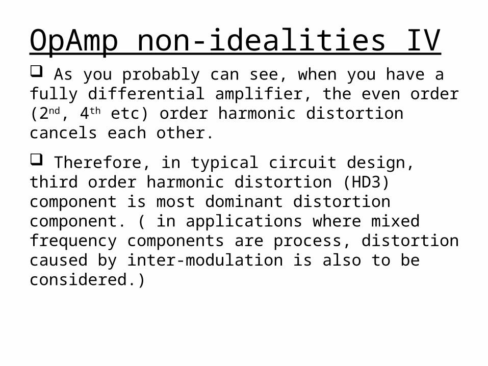
Behavioral modeling of OpAmp Behavioral models is preferred to include as many non-idealities of OpAmp as possible.
They are used to replace actual physical OpAmp for analysis and fast simulation.

Important amplifier circuits I• Inverting amplifer
• AC-coupled inverting amplifier
• Summing amplifier
• Noninverting amplifier
• AC-coupled noninverting amplifier
• Bootstrap AC-coupled voltage follower
0
/
1
12
out
in
v
Z
RZ
RRA
0
/
1
12
out
in
v
Z
RZ
RRA
0
/
2
1
/
out
BBin
AAin
BAfv
Z
vforRZ
vforRZ
RRA
0
/1 12
out
in
v
Z
Z
RRA
0
/1 12
out
biasin
v
Z
RZ
RRA
0
1
out
in
v
Z
Z
A
Graphs from Prentice Hall

Important amplifier circuits II• Differential amplifier
• Instrumentation qualify Diff Amp
• Voltage-to-current converter
• Howland voltage-to-current converter for grounded load
• Current-to-voltage amplifier
• Current amplifier
0
143
out
in
Z
vforRRZ
0
out
in
Z
Z
out
in
finom
Z
Z
RviG /1/
out
Lin
m
Z
RRRRZ
RG
)/(
/1
221
2
0
0
out
in
fm
Z
Z
RR
out
in
vi
Z
Z
RRA
0
)/1( 12
Graphs from Prentice Hall

Important amplifier circuits III• Integrator circuit: produces an
output voltage proportional to the running time integral of the input signal
• Differentiator circuit: produces an output proportional to the time derivative of the input voltage
Graphs from Prentice Hall