Embed Size (px)
Citation preview

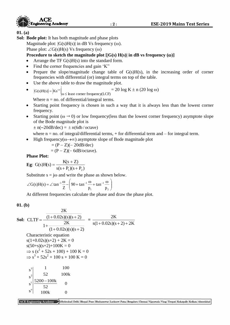
: 2 : ESE-2019 Mains Test Series
ACE Engineering Academy Hyderabad|Delhi|Bhopal|Pune|Bhubaneswar|Lucknow|Patna|Bengaluru|Chennai|Vijayawada|Vizag|Tirupati|Kukatpally|Kolkata|Ahmedabad
3
2
1
o
1 100s
52 100ks
5200 100k0s
52s 100k 0
01. (a) Sol: Bode plot: It has both magnitude and phase plots
Magnitude plot: |G(s)H(s)| in dB Vs frequency ().
Phase plot: G(s)H(s) Vs frequency ()
Procedure to sketch the magnitude plot [|G(s) H(s)| in dB vs frequency ()]
Arrange the TF G(s)H(s) into the standard form.
Find the corner frequencies and gain ‘K”
Prepare the slope/magnitude change table of G(s)H(s), in the increasing order of corner
frequencies with differential (or) integral terms on top of the table.
Use the above table to draw the magnitude plot.
)LCF(frequencycornerleastKs)s(H)s(G n
= 20 log K n (20 log )
Where n = no. of differential/integral terms.
Starting point frequency is chosen in such a way that it is always less than the lowest corner
frequency.
Starting point ( 0) or low frequency(less than the lowest corner frequency) asymptote slope
of the Bode magnitude plot is
± n(20dB/dec) = )octave/db6(n
where n = no. of integral/differential terms, + for differential term and – for integral term.
High frequency() asymptote slope of Bode magnitude plot
= (P Z)( 20dB/dec)
= (P Z)( 6dB/octave).
Phase Plot:
Eg: )P)(sPs(s
)ZK(sG(s)H(s)
21
Substitute s = j and write the phase as shown below.
2
1
1
11
ptan
ptan90
Ztan)s(H)s(G
At different frequencies calculate the phase and draw the phase plot.
01. (b)
Sol:
2K
(1 0.02s)(s)(s 2)CLTF
2K1
(1 0.02s)(s)(s 2)
= 2K
s(1 0.02s)(s 2) 2K
Characteristic equation
s(1+0.02s)(s+2) + 2K = 0
s(50+s)(s+2)+100K = 0
s (s2 + 52s + 100) + 100 K = 0
s3 + 52s
2 + 100 s + 100 K = 0
: 3 : Electronics & Telecommunication Engineering
ACE Engineering Academy Hyderabad|Delhi|Bhopal|Pune|Bhubaneswar|Lucknow|Patna|Bengaluru|Chennai|Vijayawada|Vizag|Tirupati|Kukatpally|Kolkata|Ahmedabad
For system to be stable,
100 K > 0 K > 0
5200 – 100 K > 0
52 > K
System is stable for 0 < K < 52
Maximum value of K = 52
01. (c)
Sol: The convolution property states that the convolution of two signals in time domain is equivalent to
the multiplication of their spectra in frequency domain. This is called the time convolution theorem.
If 1
FT
1 Xtx and 2
FT
2 Xtx
Then 21
FT
21 XXtx*tx
Proof: We know that the convolution of two signals x1(t) and x2(t) is given by
dtxxtx*tx 2121
dtedtxxtx*txF tj
2121
Interchanging the order of integration, we have
ddtetxxtx*txF tj
2121
Substituting t – = P in the second integration, we have
t = p + and dt = dp
ddpepxxtx*txF pj
2121
dedpepxx jpj
21
deXx j
21
212
j
1 XXXdex
21
FT
21 XXtx*tx
01. (d) Sol: let, x(t) = L
–1[X(s)]
1s
1sslogL
2
1
1s
1sslogtxL
2
= log s(s + 1) – log (s2 + 1)
= log s + log (s + 1) – log (s2 + 1)

: 4 : ESE-2019 Mains Test Series
ACE Engineering Academy Hyderabad|Delhi|Bhopal|Pune|Bhubaneswar|Lucknow|Patna|Bengaluru|Chennai|Vijayawada|Vizag|Tirupati|Kukatpally|Kolkata|Ahmedabad
1slog1slogslogds
dttxL 2
1s
s2
1s
1
s
12
1s
s2
1s
1
s
1Ltxt
2
1
1s
sL2
1s
1L
s
1L
2
111
= [– 1 – e–t
+ 2 cos(t)] u(t)
tut
1etcos2tx
t
01. (e)
Sol:
#include <stdio.h>
void main()
{
int number, i;
printf("Enter a positive integer: ");
scanf("%d",&number);
printf("Factors of %d are: ", number);
for (i = 1; i < = number; ++i)
{
if (number%i = = 0)
{
printf("%d ", i);
}
}
}
01. (f)
Sol: The 8051 micro controller can recognize five different interrupts during its normal execution.
They are mentioned in below.
1. Timer0 overflow interrupt - TF0
2. Timer1 overflow interrupt - TF1
3. External hardware interrupt - INT0
4. External hardware interrupt - INT1
5. Serial communication interrupt - RI/TI
The timer and serial interrupts are internally generated by the controller, whereas the external
interrupts (INT0, INT1) are generated by additional interfacing devices or switches that are
externally connected to the microcontroller. These external interrupts can be edge triggered or level
triggered.
Interrupt vector table:
Interrupt source Address
INT0
TF0
INT1
TF1
RI/TI
0003H
000BH
0013H
001BH
0023H
: 5 : Electronics & Telecommunication Engineering
ACE Engineering Academy Hyderabad|Delhi|Bhopal|Pune|Bhubaneswar|Lucknow|Patna|Bengaluru|Chennai|Vijayawada|Vizag|Tirupati|Kukatpally|Kolkata|Ahmedabad
Priority table:
Interrupt source Priority within level
INT0
TF0
INT1
TF1
RI/TI
Highest
lowest
02. (a)
Sol:
(i) When H(S) = 1 + s
Closed loop transfer function
G(s)
M1 G(s).H(s)
K
s s p
K1 1 s
s s p
2
K
s ps K K s
2
KM
s s p K K
Sensitivity with respect to K:
M
K
M KS
K M
2
22
2
s s p K K 1 K.(s 1) K
Ks s P K Ks s p K K
2
2
s sp
s s p K K
2
2
s 3s
s s 3 0.14 12 12
2
M
K 2
s 3sS
s 4.68s 12
Sensitivity with respect to P:
M
P.
P
MSM
P
22
2
sK p
Ks s p K Ks s p K K
2 2
sp 3s
s s p K K s 4.68s 12
: 6 : ESE-2019 Mains Test Series
ACE Engineering Academy Hyderabad|Delhi|Bhopal|Pune|Bhubaneswar|Lucknow|Patna|Bengaluru|Chennai|Vijayawada|Vizag|Tirupati|Kukatpally|Kolkata|Ahmedabad
Sensitivity with respect to :
M
.M
SM
2
22
2
sK.
Ks s p K Ks s p K K
= K)Kp(ss
sK2
M
2
1.68sS
s 4.68s 12
(ii) O.L.T.F G(s)H(s) = 3s2s
K2
G.M =
pc|jHjG|
1
For pc, G(j)H(j) = –180
–2 tan–1
2 – tan
–1
3 = – 180
tan–1
41
2+ tan
–1
3= 180
41
2+
3 = 0
314
2
2 = 16
Phase crossover frequency, pc = 4 rad/sec
Given G.M 3
3
K
94 22
K
3
5416
K 3
100
: 7 : Electronics & Telecommunication Engineering
ACE Engineering Academy Hyderabad|Delhi|Bhopal|Pune|Bhubaneswar|Lucknow|Patna|Bengaluru|Chennai|Vijayawada|Vizag|Tirupati|Kukatpally|Kolkata|Ahmedabad
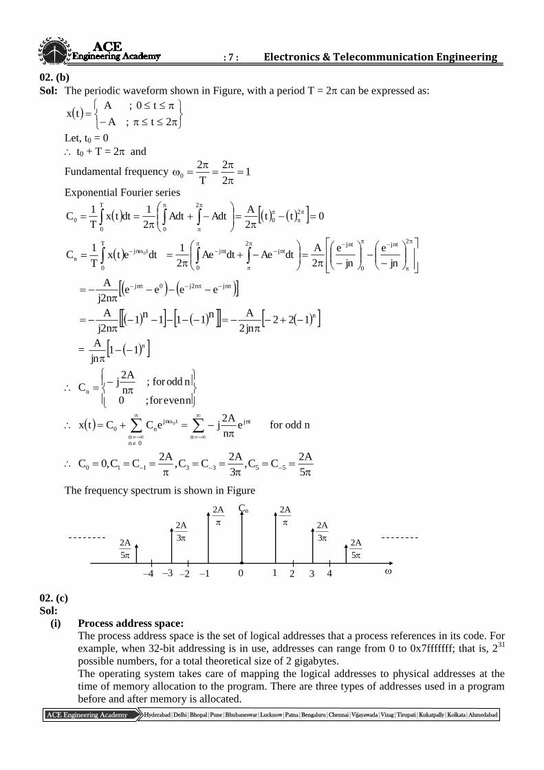
02. (b)
Sol: The periodic waveform shown in Figure, with a period T = 2 can be expressed as:
2t;A
t0;Atx
Let, t0 = 0
t0 + T = 2 and
Fundamental frequency 12
2
T
20
Exponential Fourier series
0tt2
AAdtAdt
2
1dttx
T
1C
T
0
2
0
0
2
0
dtetxT
1C
T
0
tjn
n0
2jnt
0
jnt2
jnt
0
jnt
jn
e
jn
e
2
AdtAedtAe
2
1
jnn2j0jn eeeen2j
A
n122
jn2
An111
n1
n2j
A
= n11
jn
A
nevenfor;0
noddfor;n
A2j
Cn
0nn n
jnttjn
n0 en
A2jeCCtx 0 for odd n
5
A2CC,
3
A2CC,
A2CC,0C 5533110
The frequency spectrum is shown in Figure
02. (c)
Sol:
(i) Process address space: The process address space is the set of logical addresses that a process references in its code. For
example, when 32-bit addressing is in use, addresses can range from 0 to 0x7fffffff; that is, 231
possible numbers, for a total theoretical size of 2 gigabytes.
The operating system takes care of mapping the logical addresses to physical addresses at the
time of memory allocation to the program. There are three types of addresses used in a program
before and after memory is allocated.
–4 1
5
A2
–2 0 –3 –1 2 3 4
3
A2
A2
A2
3
A2
5
A2
Cn
: 8 : ESE-2019 Mains Test Series
ACE Engineering Academy Hyderabad|Delhi|Bhopal|Pune|Bhubaneswar|Lucknow|Patna|Bengaluru|Chennai|Vijayawada|Vizag|Tirupati|Kukatpally|Kolkata|Ahmedabad
Memory Addresses & Description
1. Symbolic addresses:
The addresses used in a source code. The variable names, constants and instruction labels are the
basic elements of the symbolic address space.
2. Relative addresses:
At the time of compilation, a compiler converts symbolic addresses into relative addresses.
3. Physical addresses:
The loader generates these addresses at the time when a program is loaded into main memory.
Virtual and physical addresses are the same in compile-time and load-time address-binding
schemes. Virtual and physical addresses differ in execution-time address-binding scheme.
(ii) Static vs Dynamic Loading
The choice between Static or Dynamic Loading is to be made at the time of computer program
being developed. If you have to load your program statically, then at the time of compilation, the
complete programs will be compiled and linked without leaving any external program or module
dependency. The linker combines the object program with other necessary object modules into
an absolute program, which also includes logical addresses.
If you are writing a dynamically loaded program, then your compiler will compile the program
and for all the modules which you want to include dynamically, only references will be provided
and rest of the work will be done at the time of execution.
At the time of loading, with static loading, the absolute program (and data) is loaded into
memory in order for execution to start.
If you are using dynamic loading, dynamic routines of the library are stored on a disk in
relocatable form and are loaded into memory only when they are needed by the program.
(iii) Static vs Dynamic linking
As explained above, when static linking is used, the linker combines all other modules needed by
a program into a single executable program to avoid any runtime dependency.
When dynamic linking is used, it is not required to link the actual module or library with the
program, rather a reference to the dynamic module is provided at the time of compilation and
linking. Dynamic Link Libraries (DLL) in Windows and Shared Objects in Unix are good
examples of dynamic libraries.
(iv) Fragmentation in OS
As processes are loaded and removed from memory, the free memory space is broken into little
pieces. It happens after sometimes that processes cannot be allocated to memory blocks
considering their small size and memory blocks remains unused. This problem is known as
Fragmentation.
Fragmentation is of two types:
1. External fragmentation:
Total memory space is enough to satisfy a request or to reside a process in it, but it is not
contiguous, so it cannot be used.
2. Internal fragmentation:
Memory block assigned to process is bigger. Some portion of memory is left unused, as it
cannot be used by another process.
: 9 : Electronics & Telecommunication Engineering
ACE Engineering Academy Hyderabad|Delhi|Bhopal|Pune|Bhubaneswar|Lucknow|Patna|Bengaluru|Chennai|Vijayawada|Vizag|Tirupati|Kukatpally|Kolkata|Ahmedabad
03. (a)
Sol: (i) Principle of Argument states that let F(s) be an analytic function and if an arbitrary closed
clockwise contour is chosen in s-plane, so that F(s) is analytic at every point on the closed
contour in s-plane then the corresponding F(s) plane contour mapped in the F(s) plane will
encircle the origin, N times in anticlockwise direction, where N is the difference between the
number of poles and number of zeros of F(s) that are encircled by the chosen closed contour in
s-plane mathematically, it is expressed as, N = P – Z
(ii) The loop transfer function, G(s) H(s) is expressed as
G(s) H(s) = [1 + G(s) H(s)] –1 = F(s) – 1
From above equation, it can be concluded that contour of F(s) drawn with respect to origin of
F(s) plane is same as contour of F(s) – 1 drawn with respect to –1 + j0 of F(s) plane. We know
that F(s) = 1 + G(s) H(s) is the characteristic equation, origin (0, 0) is the critical point for F(s).
(–1, 0) is the critical point for F(s) –1 = G(s)H(s)
The critical point in using the Nyquist criterion is (1, j0) in G(s)H(s) plane and not the
origin (0, j0).
(iii) For a minimum phase transfer function, no right hand poles for G(s)H(s) should be present.
For stability, the polar plot of a minimum phase system should not enclose (–1, j0) critical point
Polar plot is sufficient to determine the stability of a system.
03. (b) Sol: The energy of a signal x(t) is given by
dttuedttxE2
t42
=
0 0 0
t8t8
2t4 joule
8
1
8
edtedte
Now, according to Parseval’s theorem, we have
dX2
1E
2
dtetuetxFX tjt4
=
j4
1
j4
edte
00
tj4tj4
224
1X
4tan
8
1d
4
1
2
1E 1
22
= joule8
1
228
1
Thus, from the above equations, we see that energy is same in both the cases.
Hence Parseval’s theorem is verified.

: 10 : ESE-2019 Mains Test Series
ACE Engineering Academy Hyderabad|Delhi|Bhopal|Pune|Bhubaneswar|Lucknow|Patna|Bengaluru|Chennai|Vijayawada|Vizag|Tirupati|Kukatpally|Kolkata|Ahmedabad
03. (c)
Sol: 1. First Approach (Using Logical-AND operator)
#include <stdio.h>
void main()
{
int A, B, C;
printf("Enter the numbers A, B and C: ");
scanf("%d %d %d", &A, &B, &C);
if (A >= B && A >= C)
printf("%d is the largest number.", A);
if (B >= A && B >= C)
printf("%d is the largest number.", B);
if (C >= A && C >= B)
printf("%d is the largest number.", C);
}
2. Second Approach (Using Nested if-else)
#include <stdio.h>
void main()
{
int A, B, C;
printf("Enter three numbers: ");
scanf("%d %d %d", &A, &B, &C);
if (A >= B) {
if (A >= C)
printf("%d is the largest number.", A);
else
printf("%d is the largest number.", C);
}
else{
if (B >= C)
printf("%d is the largest number.", B);
else
printf("%d is the largest number.", C);
}
}
03. (d)
Sol: From Deal Grove growth law,
x2 + Ax = B(t+to)
Where x - thickness of oxide layer
t - time required
to = initial time
The above expression can be rearranged as
)1___(tA/B
x
B
xt o
2
: 11 : Electronics & Telecommunication Engineering
ACE Engineering Academy Hyderabad|Delhi|Bhopal|Pune|Bhubaneswar|Lucknow|Patna|Bengaluru|Chennai|Vijayawada|Vizag|Tirupati|Kukatpally|Kolkata|Ahmedabad
(i) Dry oxidation:
Given that initial oxide thickness xo = 0.020m
A/B
x
B
xt o
2
oo
sec/m1063.2
m020.0
sec/m1011.1
m020.0626
2
= 360.36 + 7604.56
to = 7965 sec
now from equation (1)
o
2
tA/B
x
B
xt
79651063.2
120.0
1011.1
120.066
2
= 50630 sec
T = 14.06hr
(ii) Wet oxidation: Since no, initial oxidation is given in wet oxidation,
A/B
x
B
xt
2
55
2
1020.4
120.0
1031.4
120.0
= 334.1 + 2857.1
t = 3189 sec
t = 0.886hr
Comment:
Clearly, wet oxidation is much faster than dry oxidation in general, a processing time of 14.06hrs is
unacceptably long in a modern manufacturing environment. This result clearly illustrates the
"Throughput" advantage of wet oxidation over dry oxidation. However, dry oxidation is
advantageous for fabrication of very thin oxides since the interface state density for dry oxides is
generally lower.
04. (a)
Sol: x(n) X(k)
kXemnxmk
N
2j
N
DFT nk
N
2j1N
0n
NN emnxmnx
nk
N
2j1N
mn
N
nkN
2j1m
0n
N emnxemnx
Since, x((n – m))N = x(N – m + n)
nk
N
2j1m
0n
nkN
2j1m
0n
N enmNxemnx
: 12 : ESE-2019 Mains Test Series
ACE Engineering Academy Hyderabad|Delhi|Bhopal|Pune|Bhubaneswar|Lucknow|Patna|Bengaluru|Chennai|Vijayawada|Vizag|Tirupati|Kukatpally|Kolkata|Ahmedabad
C1
R2
+
+ R1
Vi V0
Let, N – m + n = ℓ
kmN
N
2j1N
mN
nkN
2j1m
0n
N exemnx
km
N
2j1N
mN
ex
Similarly, km
N
2jm1N
0
nkN
2j1N
mn
N exemnx
So, DFT
km
N
2j1N
mN
kmN
2j1mN
0
N exexmnx
k
N
2j1N
0
mkN
2j
exe
)k(Xemk
N
2j
04. (b)
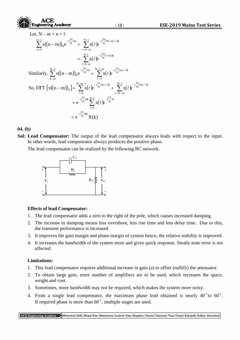
Sol: Lead Compensator: The output of the lead compensator always leads with respect to the input.
In other words, lead compensator always produces the positive phase.
The lead compensator can be realized by the following RC network.
Effects of lead Compensator:
1. The lead compensator adds a zero to the right of the pole, which causes increased damping.
2. The increase in damping means less overshoot, less rise time and less delay time. Due to this,
the transient performance is increased
3. It improves the gain margin and phase margin of system hence, the relative stability is improved.
4. It increases the bandwidth of the system more and gives quick response. Steady state error is not
affected.
Limitations:
1. This lead compensator requires additional increase in gain (a) to offset (nullify) the attenuator.
2. To obtain large gain, more number of amplifiers are to be used, which increases the space,
weight and cost.
3. Sometimes, more bandwidth may not be required, which makes the system more noisy.
4. From a single lead compensator, the maximum phase lead obtained is nearly 400to 60
0.
If required phase is more than 60 0 , multiple stages are used.
: 13 : Electronics & Telecommunication Engineering
ACE Engineering Academy Hyderabad|Delhi|Bhopal|Pune|Bhubaneswar|Lucknow|Patna|Bengaluru|Chennai|Vijayawada|Vizag|Tirupati|Kukatpally|Kolkata|Ahmedabad
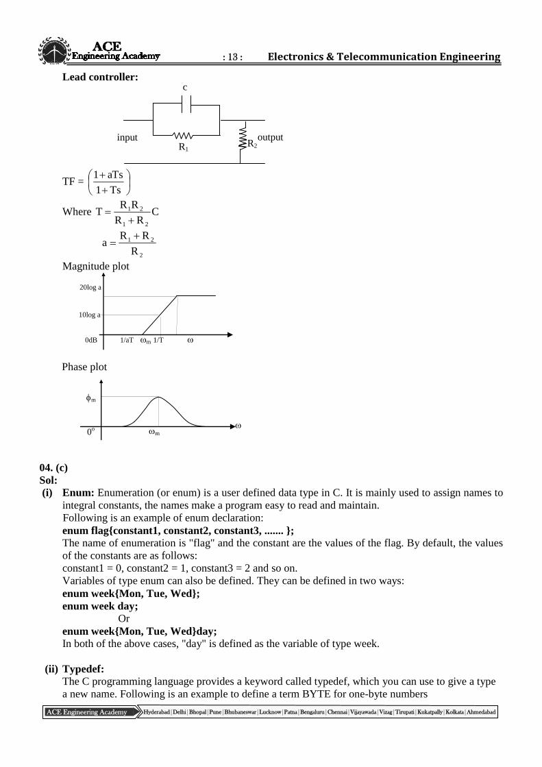
Lead controller:
TF =
Ts1
aTs1
Where CRR
RRT
21
21
2
21
R
RRa
Magnitude plot
Phase plot
04. (c)
Sol:
(i) Enum: Enumeration (or enum) is a user defined data type in C. It is mainly used to assign names to
integral constants, the names make a program easy to read and maintain.
Following is an example of enum declaration:
enum flag{constant1, constant2, constant3, ....... };
The name of enumeration is "flag" and the constant are the values of the flag. By default, the values
of the constants are as follows:
constant1 = 0, constant2 = 1, constant3 = 2 and so on.
Variables of type enum can also be defined. They can be defined in two ways:
enum week{Mon, Tue, Wed};
enum week day;
Or
enum week{Mon, Tue, Wed}day;
In both of the above cases, "day" is defined as the variable of type week.
(ii) Typedef:
The C programming language provides a keyword called typedef, which you can use to give a type
a new name. Following is an example to define a term BYTE for one-byte numbers
20log a
0dB 1/aT m 1/T
10log a
m
m 0o
R1 R2 input
c
input output
: 14 : ESE-2019 Mains Test Series
ACE Engineering Academy Hyderabad|Delhi|Bhopal|Pune|Bhubaneswar|Lucknow|Patna|Bengaluru|Chennai|Vijayawada|Vizag|Tirupati|Kukatpally|Kolkata|Ahmedabad
typedef unsigned char BYTE;
After this type definition, the identifier BYTE can be used as an abbreviation for the type unsigned
char, for example..
BYTE b1, b2;
By convention, uppercase letters are used for these definitions to remind the user that the type name
is really a symbolic abbreviation, but you can use lowercase, as follows
typedef unsigned char byte;
You can use typedef to give a name to your user defined data types as well. For example, you can
use typedef with structure to define a new data type and then use that data type to define structure
variables directly as follows
# include <stdio.h>
# include <string.h>
typedef struct Books {
char title[50];
char author[50];
char subject[100];
int book_id;
} Book;
int main( ) {
Book book;
strcpy( book.title, "C Programming");
strcpy( book.author, "Nuha Ali");
strcpy( book.subject, "C Programming Tutorial");
book.book_id = 6495407;
printf( "Book title : %s\n", book.title);
printf( "Book author : %s\n", book.author);
printf( "Book subject : %s\n", book.subject);
printf( "Book book_id : %d\n", book.book_id);
return 0;
}
When the above code is compiled and executed, it produces the following result
Book title : C Programming
Book author : Nuha Ali
Book subject : C Programming Tutorial
Book book_id : 6495407
04. (d)
Sol: The given second order system
tFcdt
db
dt
da
2
2
Taking Laplace transform on both sides
2as (s) bs (s) c (s) F(s)
2as bs c (s) F(s)
Transfer function 2
(s) 1
F(s) as bs c
: 15 : Electronics & Telecommunication Engineering
ACE Engineering Academy Hyderabad|Delhi|Bhopal|Pune|Bhubaneswar|Lucknow|Patna|Bengaluru|Chennai|Vijayawada|Vizag|Tirupati|Kukatpally|Kolkata|Ahmedabad
Step response 2
1 1(S)
as bs c s
2
1/ a 1
b c ss s
a a
= 2
c
1 1ab cc s
s sa a
Compare with standard second system
2
n
2 2
n ns s 2 s
, we get response as
tsin1
e1)t( d
2
tn
a
cn
a
b2 n
ac
b
2
1
2
nd 1 ac
b
4
11
a
c 2
ac4
bac4
a
c 2
2
d bac4a2
1
Let assume 1ac
b
2
1
Then
ac2
bcostbac4
a2
1sin
ac4
bac4
e1
c
1t 12
2
a2
bt
05. (a)
Sol: In direct mapped cache the main memory address is divided into 3 parts (fields) as follows:
Block size = 64B = 26
B Byte offset = 6-bits
Number of blocks in cache memory sizeblock
sizecache
B64
MB256
6
208
2
2.2
= 222
Tag Cache block number Byte offset
Main memory address

: 16 : ESE-2019 Mains Test Series
ACE Engineering Academy Hyderabad|Delhi|Bhopal|Pune|Bhubaneswar|Lucknow|Patna|Bengaluru|Chennai|Vijayawada|Vizag|Tirupati|Kukatpally|Kolkata|Ahmedabad
Hence cache block no. = 22-bits
Tag size = 32–(22+6) = 4-bits
Tag directory (Meta-data) size = no. of blocks in cache * 1 entry size
= 222
* (Tag + extra bits)
= 222
* (4+2) bits
= 222
* 6 bits
= 24 * 220
bits
= 24 Mbits
= 0.3 Mbytes
05. (b)
Sol: The time required is
(i) 50 nano seconds to get the page number from associative memory and 750 nano-seconds to read
the desired word from memory.
Time = 50+750= 800 nano seconds.
(ii) Now the time when not in associative memory is
Time = 50+750+750= 1550 nano seconds
One memory access extra is required to read the page table from memory.
(iii) Effective access time
= Page number in associative memory + Page number not in associated memory.
Page number in associative memory = 0.8 * 800.
Page number not in associated memory = 0.2 * 1550.
Effective access time = 0.8 * 800 + 0.2 * 1550 = 950 nano seconds 05. (c) Sol: Given, Input x(t) = te
–3t u(t)
23s
1sX
Impulse response h(t) = 2e–4t
u(t)
4s
2sH
We know that, Output y(t) = x(t) * h(t)
Y(s) = X(s) H(s)
So, Output y(t) = L–1
[X(s) H(s)]
4s3s
2
4s
2
3s
1sHsXsY
22
Taking partial fractions, we have
4s
C
3s
B
3s
A
4s3s
2sY
22
4s
2
3s
2
3s
2sY
2
Taking inverse Laplace transform on both sides, we have the output
y(t) = 2te–3t
u(t) – 2e–3t
u(t) + 2e–4t
u(t)
Tag Cache block number Byte offset
32
4 22 6

: 17 : Electronics & Telecommunication Engineering
ACE Engineering Academy Hyderabad|Delhi|Bhopal|Pune|Bhubaneswar|Lucknow|Patna|Bengaluru|Chennai|Vijayawada|Vizag|Tirupati|Kukatpally|Kolkata|Ahmedabad
05. (d)
Sol: Given open loop transfer function
G(s) = 1s(s
)4s(K
No. of root locus branches = 2(P > Z)
No. of Asymptotes N = |P – Z| = 1
Angle of Asymptotes = 02 +1 180
P Z l = 0
1
180102 0 = 180
0
Here, only one asymptote is present, therefore centroid is not required.
Break Point CE is 0(s)(s)HKG1 11
(s)(s)HG
1K
11
1 1
s 4G (s)H (s)
s(s 1)
0)s(H)s(G
1
ds
d
ds
dK
11
04s
1)s(s
ds
d
04)(s
s)(1)(s1)4)(2s(s2
2
s2
+ 8s + 4 = 0
s = 0.6 and s = 7.4
The system is critically damped when s= 0.6 and s = 7.4 (roots are real and equal)
K = zerosfromcestandisofoductPr
polesfromcestandisofoductPr
)6.0sat(07.04.3
)4.0)(6.0(K
)4.7sat(92.134.3
)4.6)(4.7(K
j
0.6 1 4 0 7.4
(K=) (K=0) (K=0) (K=)
Fig. Root Locus diagram
: 18 : ESE-2019 Mains Test Series
ACE Engineering Academy Hyderabad|Delhi|Bhopal|Pune|Bhubaneswar|Lucknow|Patna|Bengaluru|Chennai|Vijayawada|Vizag|Tirupati|Kukatpally|Kolkata|Ahmedabad
05. (e)
Sol: Fermi potential for p-substrate and n-type poly silicon are given by
V367.0102
1045.1ln026.0
N
nln
q
KTsubstrate
16
10
A
iF
V547.01045.1
102ln026.0
n
Nln
q
KTgate
10
19
i
DF
The work function difference,
gatesubstratems
= – 0.367 – 0.547
ms = – 0.914V
Oxide capacitance per unit area
27
8
14
ox
oxox cm/F1017.1
10300
1085.897.3
tC
The depletion layer charge,
|substrate2|qN2Q FsiAbo
|367.02|1085.87.11102106.12 141619
Qbo = – 6.9710–8
c/cm2
The fixed oxide charge, Qox = qNox = 1.610–1910
10 = 1.610
–9c/cm
2
Now, threshold voltage ox
ox
ox
boFmst
C
Q
C
Q2V
7
9
7
8
1017.1
106.1
1017.1
1097.6367.02914.0
= – 0.914 + 0.734 + 0.594 – 0.0138
Vt = 0.4002V
06. (a) Sol: Arrange the given transfer function as,
)s(I
)s(Q =
J
Ks
J
fsJ
1
2
=
J
Ks
J
fs
J
1
2
Comparing denominator with s2+2ns + 2
n ,
2
n = J
K i.e. n =
J
K….. (1)
and 2n = J
f i.e.,
KJ2
f ….. (2)
Now Mp = 6% i.e., 0.06
0.06 = 21/
e
ln (0.06) = 21
: 19 : Electronics & Telecommunication Engineering
ACE Engineering Academy Hyderabad|Delhi|Bhopal|Pune|Bhubaneswar|Lucknow|Patna|Bengaluru|Chennai|Vijayawada|Vizag|Tirupati|Kukatpally|Kolkata|Ahmedabad
Solving for , = 0.667 ……. (3)
Tp = d
=
2
n 1
= 1 sec
n = 2)667.0(1
= 4.2165 rad/sec. … (4)
The Laplace transform of output is Q(s).
Now input is step of 10 Nm hence corresponding Laplace transform is,
I(s) = s
10
s
10
)s(Q =
KfsJs
12
Q(s) = KfsJss
12
The steady state of output can be obtained by final value theorem.
Steady state output = )s(QsLim0s
0.5 = KfsJss
10.sLim
20s =
k
10
K = 20
Equating (1) and (4), 4.2165 = J
K
4.2165 = J
20
J = 1.1249
From equation (2), 0.667 = KJ2
f
0.067 = 1249.1202
f
f = 6.3274
06. (b)
Sol: Given
1n
n0n0 tncosCCtx
(i) Autocorrelation:
Autocorrelation of function x(t) is given by
2/T
2/TT
dttxtxT
1LtR
2/T
2/T 1n
n00n0
1n
n0n0T
ntncosCCtncosCCT
1LtR
=
2/T
2/T 1n 1n
n0n0n00n0
2
0T
tncosCCntncosCCCT
1Lt
dtntncostncosC n00
1n
n0
2
n
: 20 : ESE-2019 Mains Test Series
ACE Engineering Academy Hyderabad|Delhi|Bhopal|Pune|Bhubaneswar|Lucknow|Patna|Bengaluru|Chennai|Vijayawada|Vizag|Tirupati|Kukatpally|Kolkata|Ahmedabad
=
2/T
2/T 1n
n00n0
2/T
2/TT
2
0T
dtntncosCCT
1LtdtC
T
1Lt
2/T
2/T 1n
n0n0T
dttncosCCT
1Lt
2/T
2/T 1n
n00n0
2
nT
dtntncostncosCT
1Lt
=
1n
2/T
2/T
n00n0
2
n
T
2
0 dtntncostncos2T2
CLt00C
=
1n
2/T
2/T
0n00
2
n
T
2
0 dtncos2ntn2cosT2
CLtC
=
1n
2/T
2/T 1n
0
2
n
T
2
00
2
n
T
2
02
T
2
Tncos
T2
CLtCdtncos
T2
CLtC
=
1n
0
2
n
T
2
0 TncosT2
CLtC
1n
0
2
n
2
0 ncosC2
1CR
Power spectral density (PSD) and autocorrelation form a Fourier transform pair
PSD = F[R()]
1n
0
2
n
2
0 ncosC2
1CFPSD
=
1n
00
2
n
2
0 nnC2
12C
06. (c)
Sol:
(i) Memory size = 4GB
word size = 64-bits = 8 Bytes
Memory size (in words) = B8
GB4
= 0.5G words
= 512 M words
= 229
words
Address size = log2(229
) = 29.bits
: 21 : Electronics & Telecommunication Engineering
ACE Engineering Academy Hyderabad|Delhi|Bhopal|Pune|Bhubaneswar|Lucknow|Patna|Bengaluru|Chennai|Vijayawada|Vizag|Tirupati|Kukatpally|Kolkata|Ahmedabad
(ii) Drawbacks in each Scheduling Policy
A) FIFO replacement policy:
1. A page which is being accessed quite often may also get replaced because it arrived earlier than
those present
2. Ignores locality of reference. A page which was referenced last may also get replaced, although
there is high probability that the same page may be needed again.
B) LRU replacement policy:
1. A good scheme because focuses on replacing dormant pages and takes care of locality of
reference, but
2. A page which is accessed quite often may get replaced because of not being accessed for some
time, although being a significant page may be needed in the very next access.
(iii) In direct mapped cache main memory address is divided into 3 fields as follows:
Main memory address = 32-bits given
Tag = 16-bits given
Cache block no. = 12-bits (because no. of blocks in cache = 212
)
Byte offset = 32-(16+12) = 4-bits
Block size = 24 = 16 Bytes
07. (a)
Sol: Hanning window:
2
1Nn
2
1Nfor
1N
n2cos5.05.0nwHn
= 0 otherwise
N = 11
wHn(0) = 1
wHn(1) = wHn(–1) = 0.9045
wHn(2) = wHn(–2) = 0.655
wHn(3) = wHn(–3) = 0.345
wHn(4) = wHn(–4) = 0.0945
wHn(5) = wHn(–5) = 0
The filter coefficients are obtained as
n
n4
sinnsin
de.eH2
1nh njj
dd
75.04
11
n
4
nsinnsin
Lt0h0n
d
hd(–1) = hd(1) = – 0.225
hd(–2) = hd(2) = – 0.159
hd(–3) = hd(3) = – 0.075
hd(–4) = hd(4) = 0
hd(–5) = hd(5) = 0.045
Tag Cache block no. Byte offset
Main memory address
: 22 : ESE-2019 Mains Test Series
ACE Engineering Academy Hyderabad|Delhi|Bhopal|Pune|Bhubaneswar|Lucknow|Patna|Bengaluru|Chennai|Vijayawada|Vizag|Tirupati|Kukatpally|Kolkata|Ahmedabad
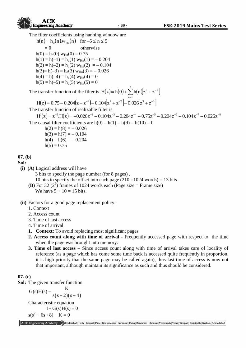
The filter coefficients using hanning window are
nw.nhnh Hnd for –5 n 5
= 0 otherwise
h(0) = hd(0) wHn(0) = 0.75
h(1) = h(–1) = hd(1) wHn(1) = – 0.204
h(2) = h(–2) = hd(2) wHn(2) = – 0.104
h(3)= h(–3) = hd(3) wHn(3) = – 0.026
h(4) = h(–4) = hd(4) wHn(4) = 0
h(5) = h(–5) = hd(5) wHn(5) = 0
The transfer function of the filter is nn5
1n
zznh0hzH
33221 zz026.0zz104.0zz204.075.0zH
The transfer function of realizable filter is
876543251 z026.0z104.0z204.0z75.0z204.0z104.0z026.0zH.zzH
The causal filter coefficients are h(0) = h(1) = h(9) = h(10) = 0
h(2) = h(8) = – 0.026
h(3) = h(7) = – 0.104
h(4) = h(6) = – 0.204
h(5) = 0.75
07. (b)
Sol: (i) (A) Logical address will have
3 bits to specify the page number (for 8 pages) .
10 bits to specify the offset into each page (210 =1024 words) = 13 bits.
(B) For 32 (25) frames of 1024 words each (Page size = Frame size)
We have 5 + 10 = 15 bits.
(ii) Factors for a good page replacement policy:
1. Context
2. Access count
3. Time of last access
4. Time of arrival
1. Context: To avoid replacing most significant pages
2. Access count along with time of arrival - Frequently accessed page with respect to the time
when the page was brought into memory.
3. Time of last access – Since access count along with time of arrival takes care of locality of
reference (as a page which has come some time back is accessed quite frequently in proportion,
it is high priority that the same page may be called again), thus last time of access is now not
that important, although maintain its significance as such and thus should be considered.
07. (c)
Sol: The given transfer function
KG(s)H(s)
s s 2 s 4
Characteristic equation
1 G(s)H(s) 0
s(s2 + 6s +8) + K = 0

: 23 : Electronics & Telecommunication Engineering
ACE Engineering Academy Hyderabad|Delhi|Bhopal|Pune|Bhubaneswar|Lucknow|Patna|Bengaluru|Chennai|Vijayawada|Vizag|Tirupati|Kukatpally|Kolkata|Ahmedabad
s3
+ 6s2 + 8s + K = 0
Apply Routh Hurwitz criteria,
s3 1 8
s2 6 K
s1
6
K48
0
s0 K
If there are any sign changes in the first column, the system is unstable. So to be stable 6
K48 > 0,
K > 0 K < 48, K > 0
0 < K < 48
For the system to be stable.
For remaining values of K system is unstable. i.e., K < 0, K > 48.
At the point of intersection of root loci with imaginary axis system is critically stable.
48 – K = 0
K = 48
Substitute K value in second row.
We will get auxiliary equation as
6s2 + K = 0
6s2 + 48 = 0
s2 + 8 = 0
s = 22j
At s = 22j , root loci intersects with imaginary axis.
07. (d)
Sol:
(i)
CPLD FPGA
1. Predictable performance
independent of internal
placement and routing
2. Functionality is
implemented by PAL like
structures
3. Suitable for low to medium
density designs
4. Regular PAL like
architecture
5. Cross bar type
interconnection type fabric
6. Can be reprogrammed a
limited number of times
1. Performance depends on the
routing implemented for a
particular application.
2. Functionality is
implemented by look up
tables.
3. Suitable for medium to high
density designs
4. More complex and register
rich architecture
5. Channel based
interconnection fabric
6. Can be reprogrammed as
many times as possible.
: 24 : ESE-2019 Mains Test Series
ACE Engineering Academy Hyderabad|Delhi|Bhopal|Pune|Bhubaneswar|Lucknow|Patna|Bengaluru|Chennai|Vijayawada|Vizag|Tirupati|Kukatpally|Kolkata|Ahmedabad
(ii)
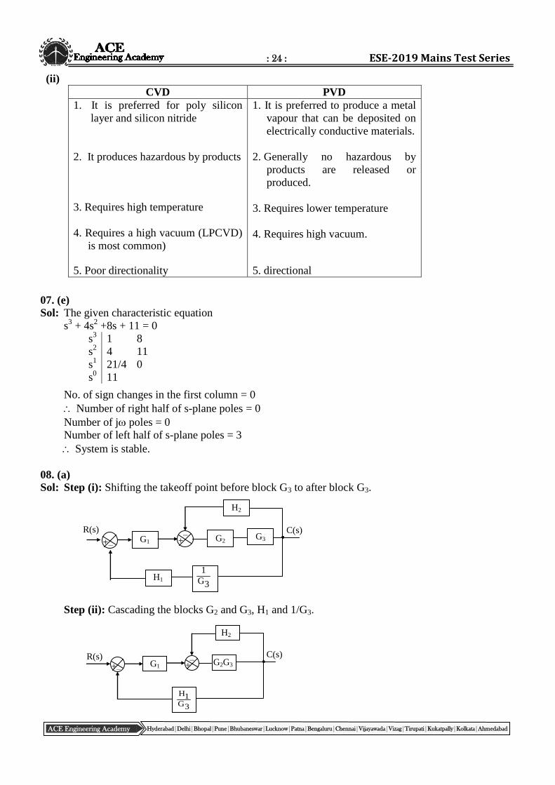
CVD PVD
1. It is preferred for poly silicon
layer and silicon nitride
2. It produces hazardous by products
3. Requires high temperature
4. Requires a high vacuum (LPCVD)
is most common)
5. Poor directionality
1. It is preferred to produce a metal
vapour that can be deposited on
electrically conductive materials.
2. Generally no hazardous by
products are released or
produced.
3. Requires lower temperature
4. Requires high vacuum.
5. directional
07. (e)
Sol: The given characteristic equation
s3 + 4s
2 +8s + 11 = 0
s3 1 8
s2 4 11
s1 21/4 0
s0 11
No. of sign changes in the first column = 0
Number of right half of s-plane poles = 0
Number of j poles = 0
Number of left half of s-plane poles = 3
System is stable.
08. (a)
Sol: Step (i): Shifting the takeoff point before block G3 to after block G3.
Step (ii): Cascading the blocks G2 and G3, H1 and 1/G3.
+ – G1 +
– G2 G3
H1
H2
R(s) C(s)
3G
1
+ – G1 +
– G2G3
H2
R(s) C(s)
3G1H
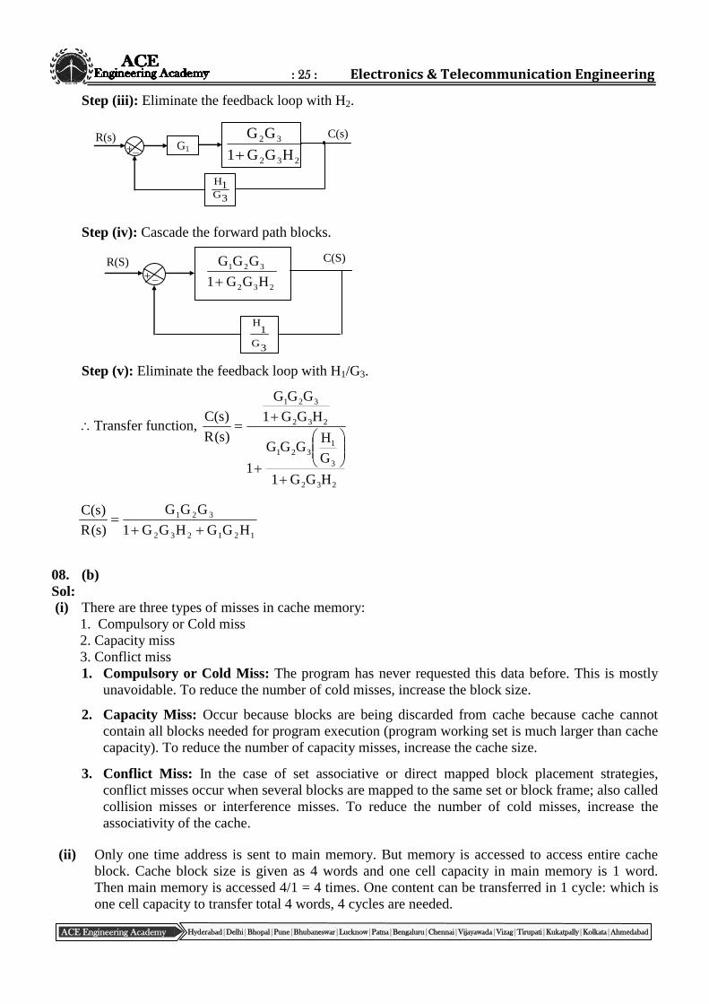
: 25 : Electronics & Telecommunication Engineering
ACE Engineering Academy Hyderabad|Delhi|Bhopal|Pune|Bhubaneswar|Lucknow|Patna|Bengaluru|Chennai|Vijayawada|Vizag|Tirupati|Kukatpally|Kolkata|Ahmedabad
Step (iii): Eliminate the feedback loop with H2.
Step (iv): Cascade the forward path blocks.
Step (v): Eliminate the feedback loop with H1/G3.
Transfer function,
232
3
1321
232
321
HGG1
G
HGGG
1
HGG1
GGG
)s(R
)s(C
121232
321
HGGHGG1
GGG
)s(R
)s(C
08. (b)
Sol: (i) There are three types of misses in cache memory:
1. Compulsory or Cold miss
2. Capacity miss
3. Conflict miss
1. Compulsory or Cold Miss: The program has never requested this data before. This is mostly
unavoidable. To reduce the number of cold misses, increase the block size.
2. Capacity Miss: Occur because blocks are being discarded from cache because cache cannot
contain all blocks needed for program execution (program working set is much larger than cache
capacity). To reduce the number of capacity misses, increase the cache size.
3. Conflict Miss: In the case of set associative or direct mapped block placement strategies,
conflict misses occur when several blocks are mapped to the same set or block frame; also called
collision misses or interference misses. To reduce the number of cold misses, increase the
associativity of the cache.
(ii) Only one time address is sent to main memory. But memory is accessed to access entire cache
block. Cache block size is given as 4 words and one cell capacity in main memory is 1 word.
Then main memory is accessed 4/1 = 4 times. One content can be transferred in 1 cycle: which is
one cell capacity to transfer total 4 words, 4 cycles are needed.
+ – G1
232
32
HGG1
GG
R(s) C(s)
3G1H
+ –
1 2 3
2 3 2
G G G
1 G G H
R(S) C(S)
3G
1H
: 26 : ESE-2019 Mains Test Series
ACE Engineering Academy Hyderabad|Delhi|Bhopal|Pune|Bhubaneswar|Lucknow|Patna|Bengaluru|Chennai|Vijayawada|Vizag|Tirupati|Kukatpally|Kolkata|Ahmedabad
Miss penalty time = Address sending time = 1
+
Memory access time = (4*10)
+
Block Transfer time = 4 * 1
45 cycles
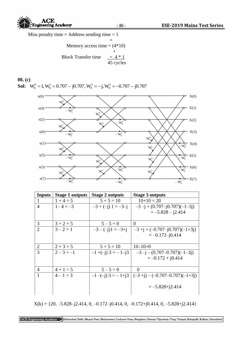
08. (c)
Sol: 707.0j707.0W,jW,707.0j707.0W,1W 3
8
2
8
1
8
0
8
X(k) = {20, –5.828–j2.414, 0, –0.172–j0.414, 0, –0.172+j0.414, 0, –5.828+j2.414}
Inputs Stage 1 outputs Stage 2 outputs Stage 3 outputs
1 1 + 4 = 5 5 + 5 = 10 10+10 = 20
4 1– 4 = –3 –3 + (–j) 1 = –3–j –3 –j + (0.707–j0.707)(–1–3j)
= –5.828 – j2.414
3 3 + 2 = 5 5 – 5 = 0 0
2 3 – 2 = 1 –3 – (–j)1 = –3+j –3 +j + (–0.707–j0.707)(–1+3j)
= –0.172–j0.414
2 2 + 3 = 5 5 + 5 = 10 10–10=0
3 2 – 3 = –1 –1 +(–j) 3 = – 1–j3 –3 –j – (0.707–0.707)(–1–3j)
= –0.172 + j0.414
4 4 + 1 = 5 5 – 5 = 0 0
1 4 – 1 = 3 –1 –(–j) 3 = – 1+j3 (–3 +j) – (–0.707–0.707)(–1+3j)
= –5.828+j2.414
0
8W
0
8W
1
8W
3
8W
2
8W
X(0)
X(1)
X(2)
X(3)
X(4)
X(5)
X(6)
X(7)
x(0)
x(4)
x(2)
x(6)
x(1)
x(5)
x(3)
x(7)
0
8W
0
8W
0
8W
0
8W 2
8W 3
8W
2
8W
1
8W
0
8W
0
8W
2
8W
0
8W 0
8W
0
8W
0
8W
0
8W
2
8W
2
8W
0
8W
: 27 : Electronics & Telecommunication Engineering
ACE Engineering Academy Hyderabad|Delhi|Bhopal|Pune|Bhubaneswar|Lucknow|Patna|Bengaluru|Chennai|Vijayawada|Vizag|Tirupati|Kukatpally|Kolkata|Ahmedabad
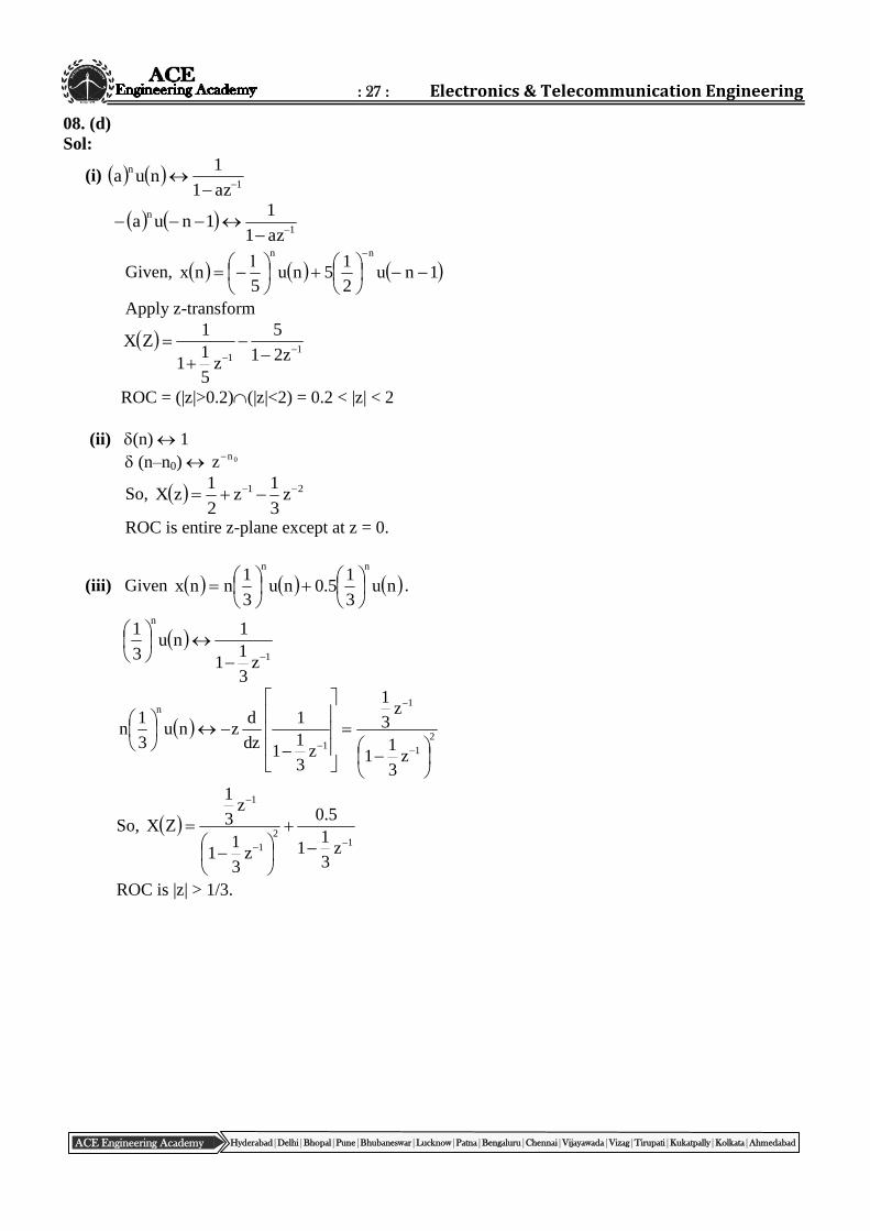
08. (d)
Sol:
(i) 1
n
az1
1nua
1
n
az1
11nua
Given, 1nu2
15nu
5nx
nn
Apply z-transform
1
1 z21
5
z5
11
1ZX
ROC = (|z|>0.2)(|z|<2) = 0.2 < |z| < 2
(ii) (n) 1
(n–n0) 0nz
So, 21 z3
1z
2
1zX
ROC is entire z-plane except at z = 0.
(iii) Given nu3
15.0nu
3
1nnx
nn
.
1
n
z3
11
1nu
3
1
2
1
1
1
n
z3
11
z3
1
z3
11
1
dz
dznu
3
1n
So, 1
2
1
1
z3
11
5.0
z3
11
z3
1
ZX
ROC is |z| > 1/3.