Embed Size (px)
Citation preview
SPIN VALVE
TRANSISTOR
SUBMITED TO SUBMITTED BY SEMINAR GUIDE
Er. AMIT KATIYAR EESHAN MISHRA Er. AJEET KUMAR SRIVASTAVA
Er. ROLI NIGAM
(SEMINAR IN CHARGE)
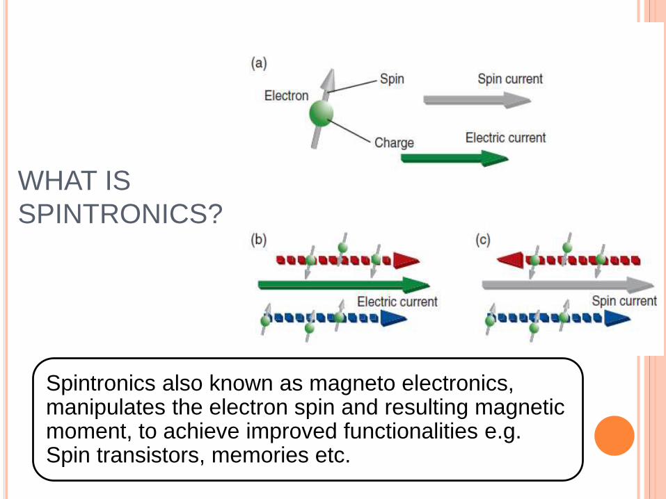
WHAT IS
SPINTRONICS?
Spintronics also known as magneto electronics, manipulates the electron spin and resulting magnetic moment, to achieve improved functionalities e.g. Spin transistors, memories etc.
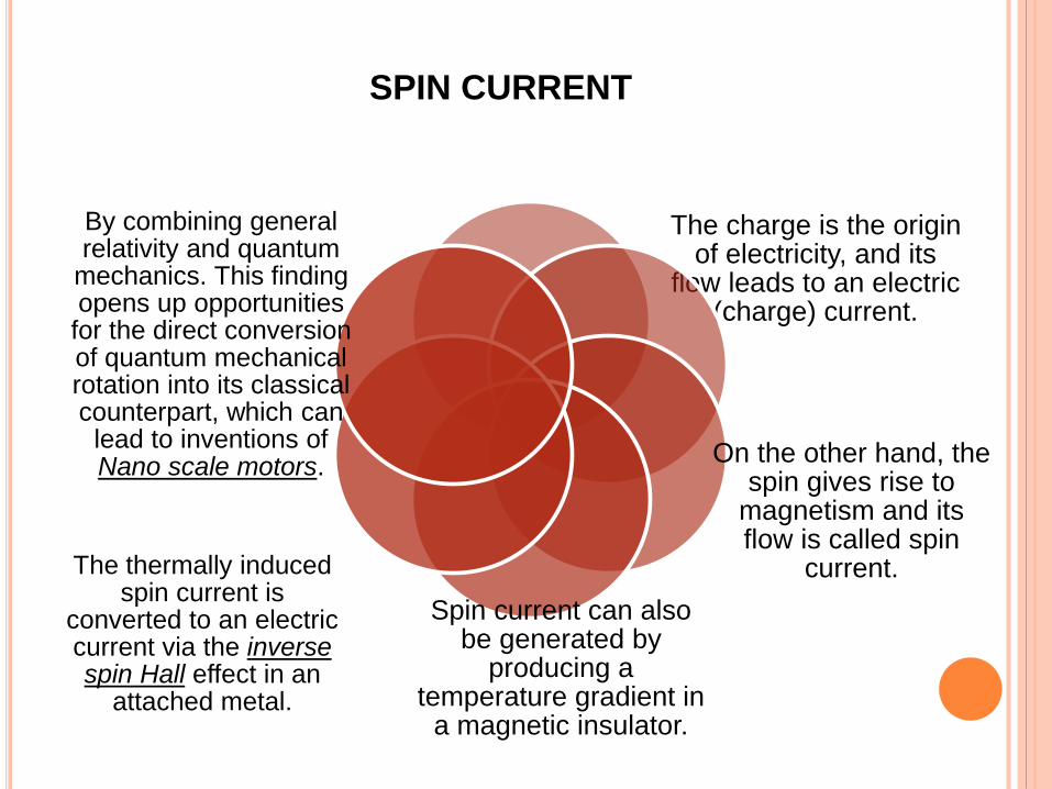
The charge is the origin of electricity, and its
flow leads to an electric (charge) current.
SPIN CURRENT
On the other hand, the spin gives rise to
magnetism and its flow is called spin
current.
Spin current can also be generated by
producing a temperature gradient in
a magnetic insulator.
The thermally induced spin current is
converted to an electric current via the inverse spin Hall effect in an
attached metal.
By combining general relativity and quantum
mechanics. This finding opens up opportunities
for the direct conversion of quantum mechanical rotation into its classical counterpart, which can
lead to inventions of Nano scale motors.
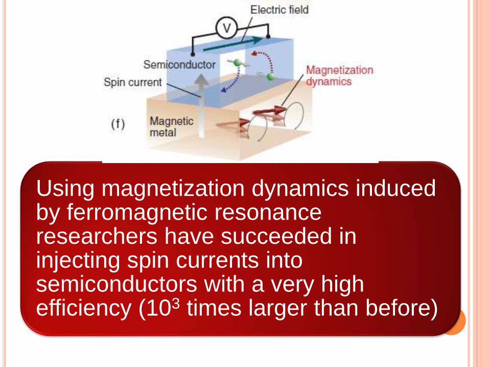
Using magnetization dynamics induced by ferromagnetic resonance researchers have succeeded in injecting spin currents into semiconductors with a very high efficiency (103 times larger than before)
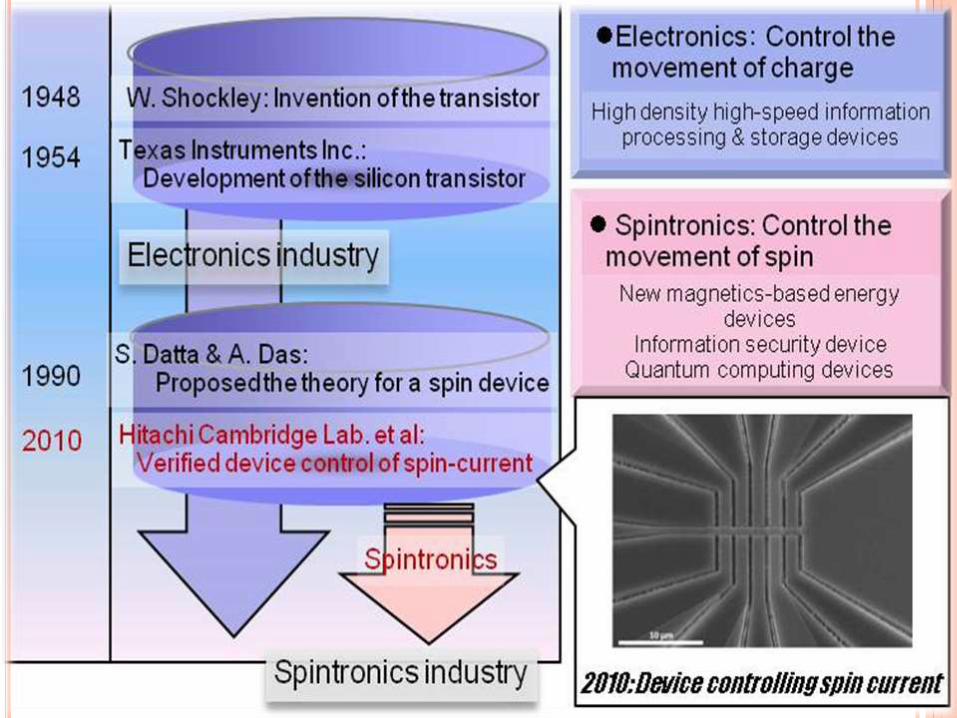
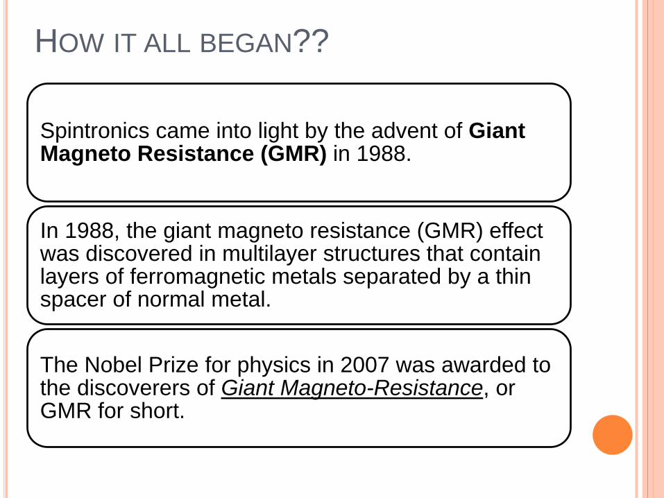
HOW IT ALL BEGAN??
Spintronics came into light by the advent of Giant Magneto Resistance (GMR) in 1988.
In 1988, the giant magneto resistance (GMR) effect was discovered in multilayer structures that contain layers of ferromagnetic metals separated by a thin spacer of normal metal.
The Nobel Prize for physics in 2007 was awarded to the discoverers of Giant Magneto-Resistance, or GMR for short.
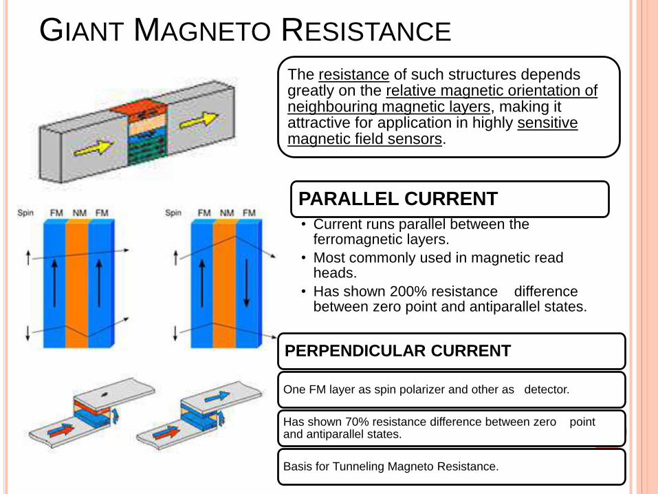
GIANT MAGNETO RESISTANCE
The resistance of such structures depends greatly on the relative magnetic orientation of neighbouring magnetic layers, making it attractive for application in highly sensitive magnetic field sensors.
PARALLEL CURRENT
• Current runs parallel between the ferromagnetic layers.
• Most commonly used in magnetic read heads.
• Has shown 200% resistance difference between zero point and antiparallel states.
PERPENDICULAR CURRENT
One FM layer as spin polarizer and other as detector.
Has shown 70% resistance difference between zero point and antiparallel states.
Basis for Tunneling Magneto Resistance.
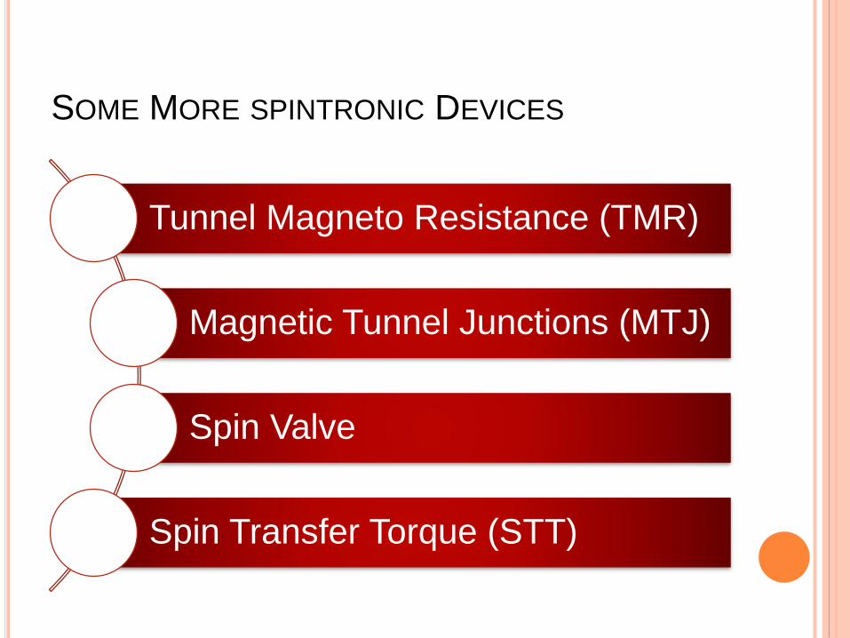
SOME MORE SPINTRONIC DEVICES
Tunnel Magneto Resistance (TMR)
Magnetic Tunnel Junctions (MTJ)
Spin Valve
Spin Transfer Torque (STT)
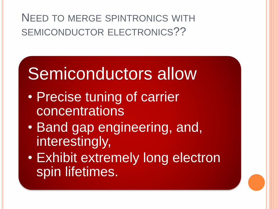
NEED TO MERGE SPINTRONICS WITH
SEMICONDUCTOR ELECTRONICS??
Semiconductors allow
• Precise tuning of carrier concentrations
• Band gap engineering, and, interestingly,
• Exhibit extremely long electron spin lifetimes.
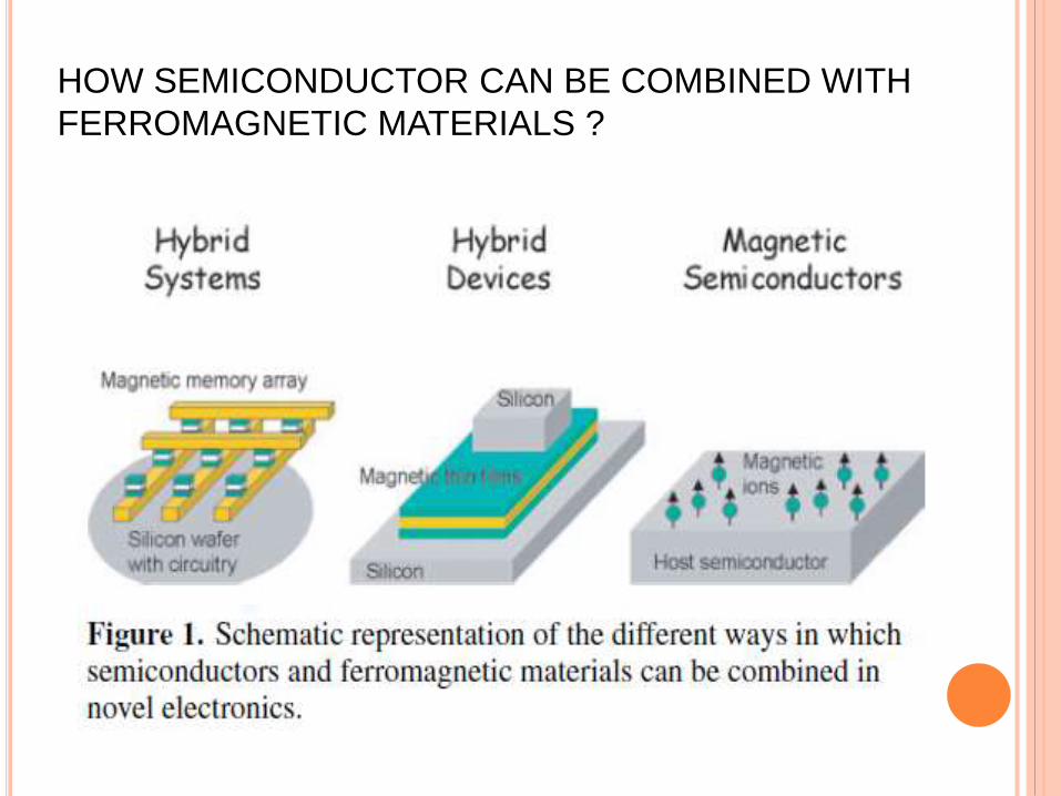
HOW SEMICONDUCTOR CAN BE COMBINED WITH
FERROMAGNETIC MATERIALS ?
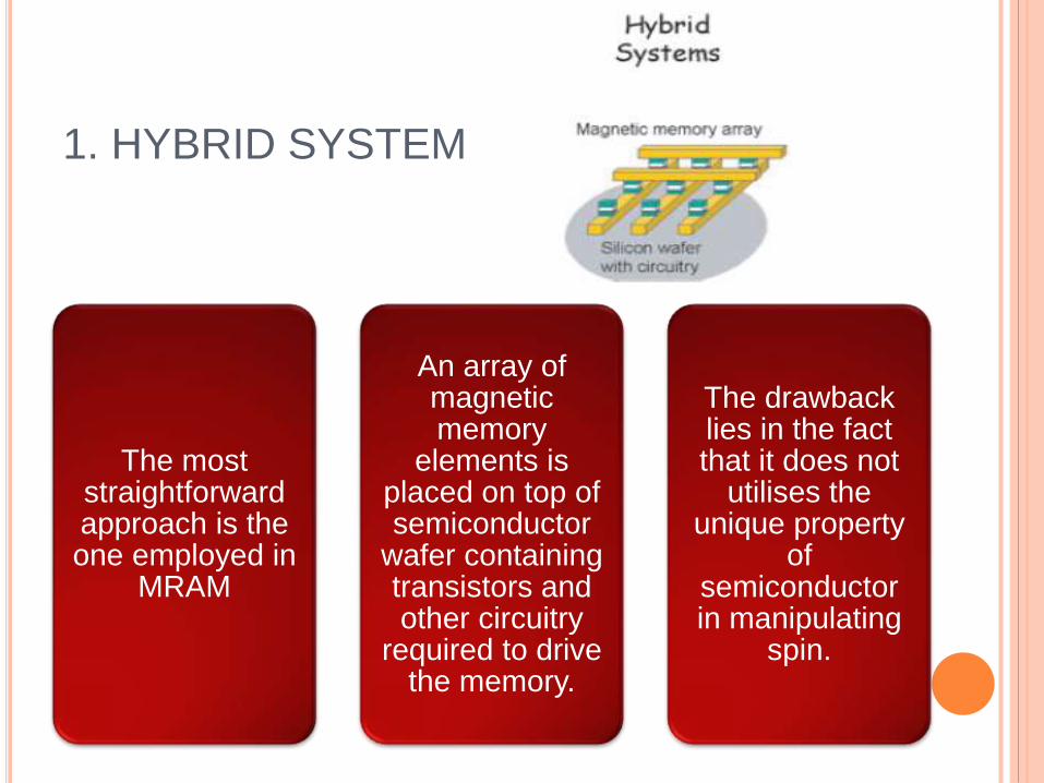
1. HYBRID SYSTEM
The most straightforward approach is the one employed in
MRAM
An array of magnetic memory
elements is placed on top of semiconductor
wafer containing transistors and other circuitry
required to drive the memory.
The drawback lies in the fact that it does not
utilises the unique property
of semiconductor in manipulating
spin.
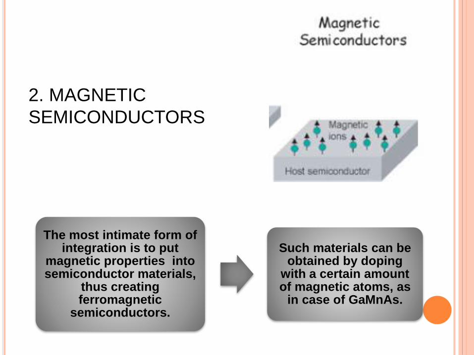
2. MAGNETIC
SEMICONDUCTORS
The most intimate form of integration is to put
magnetic properties into semiconductor materials,
thus creating ferromagnetic
semiconductors.
Such materials can be obtained by doping
with a certain amount of magnetic atoms, as
in case of GaMnAs.
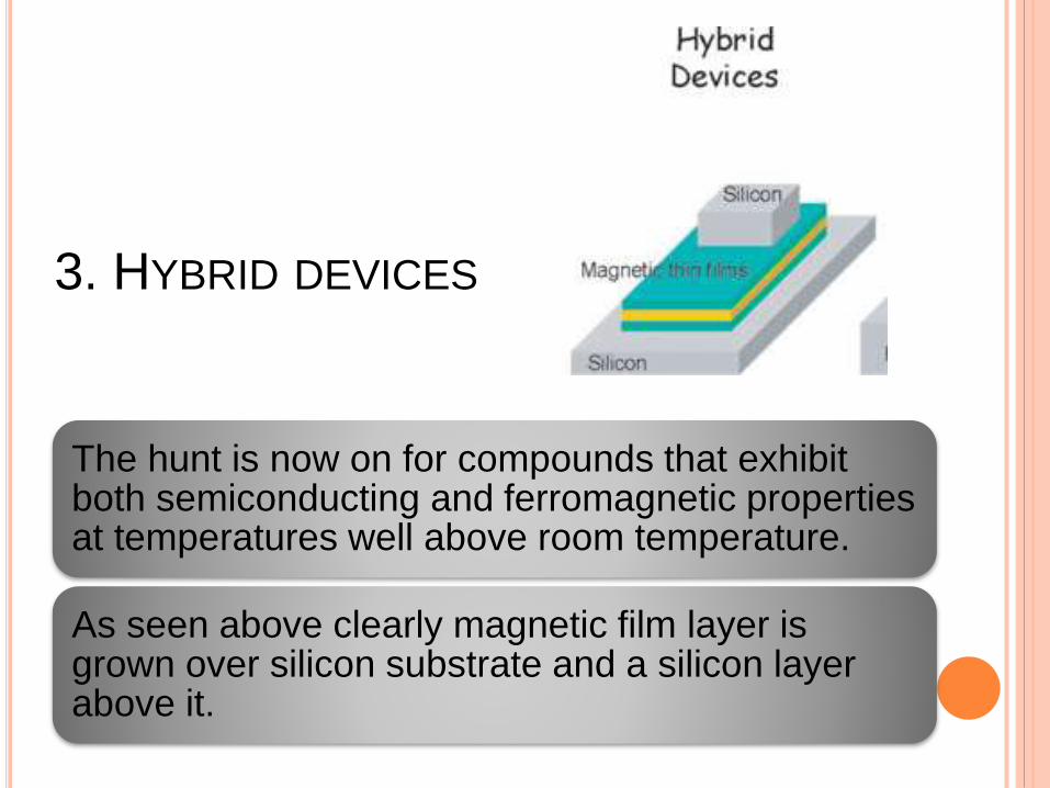
3. HYBRID DEVICES
The hunt is now on for compounds that exhibit both semiconducting and ferromagnetic properties at temperatures well above room temperature.
As seen above clearly magnetic film layer is grown over silicon substrate and a silicon layer above it.
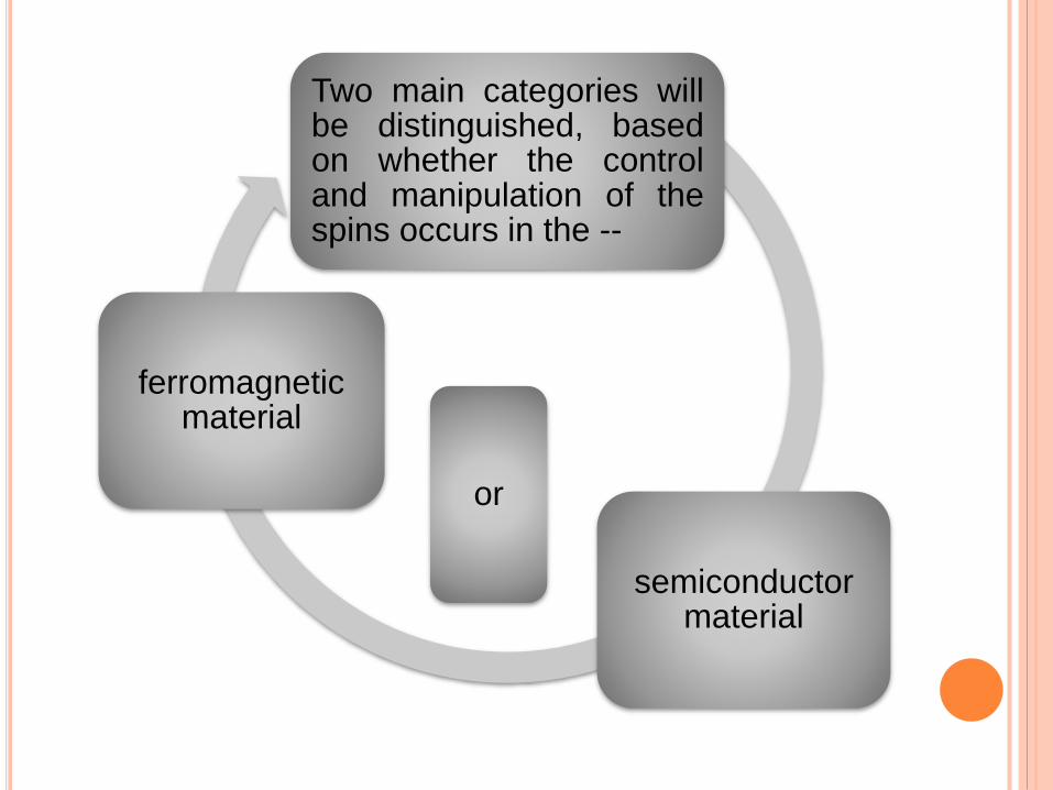
Two main categories willbe distinguished, basedon whether the controland manipulation of thespins occurs in the --
semiconductor material
or
ferromagnetic material
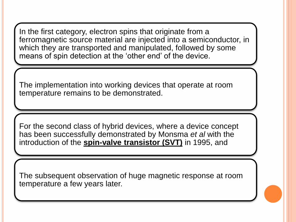
In the first category, electron spins that originate from a ferromagnetic source material are injected into a semiconductor, in which they are transported and manipulated, followed by some means of spin detection at the ‘other end’ of the device.
The implementation into working devices that operate at room temperature remains to be demonstrated.
For the second class of hybrid devices, where a device concept has been successfully demonstrated by Monsma et al with the introduction of the spin-valve transistor (SVT) in 1995, and
The subsequent observation of huge magnetic response at room temperature a few years later.
WHAT IS SPIN VALVE TRANSISTOR?
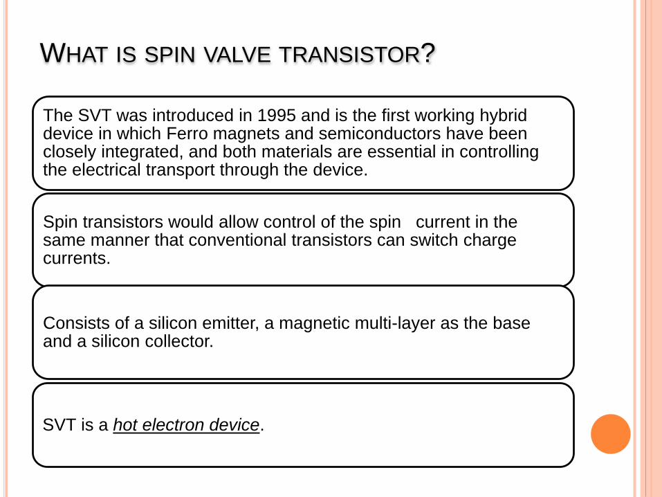
The SVT was introduced in 1995 and is the first working hybrid device in which Ferro magnets and semiconductors have been closely integrated, and both materials are essential in controlling the electrical transport through the device.
Spin transistors would allow control of the spin current in the same manner that conventional transistors can switch charge currents.
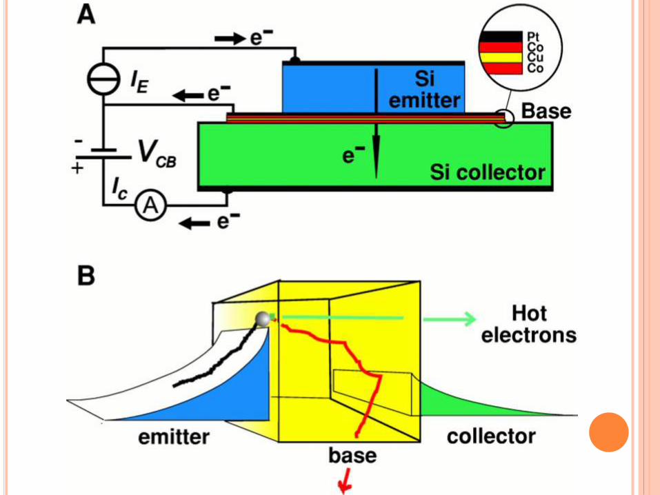
Consists of a silicon emitter, a magnetic multi-layer as the base and a silicon collector.
SVT is a hot electron device.
DEVICE CHARACTERISTICS
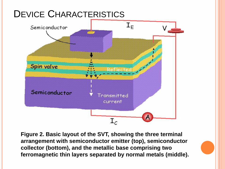
Figure 2. Basic layout of the SVT, showing the three terminal
arrangement with semiconductor emitter (top), semiconductor
collector (bottom), and the metallic base comprising two
ferromagnetic thin layers separated by normal metals (middle).
The three-terminal device has the typical emitter/base/collector structure of a (bipolar) transistor, but is different in that the base region is metallic and contains at least two magnetic layers separated by a normal metal spacer.
The two magnetic layers act as polarizer and analyserof electron spins, such that the relative orientation of the magnetization of the two layers determines the transmission of the base.
Spin dependence of the transport is in the ferromagnetic materials, the semiconductors are used to create energy barriers in the electron’s potential landscape that are essential to the operation of the device.
The resulting salient feature of the SVT is that the collector current depends on the magnetic state of the base.
They succeeded in the reproducible fabrication of SVTs that exhibit magnetocurrent effects up to 400% at room temperature, and in small magnetic fields of only a few Oe.
the SVT is based on the spin-dependent transport of non-equilibrium, so-called hot electrons, rather than Fermi electrons.
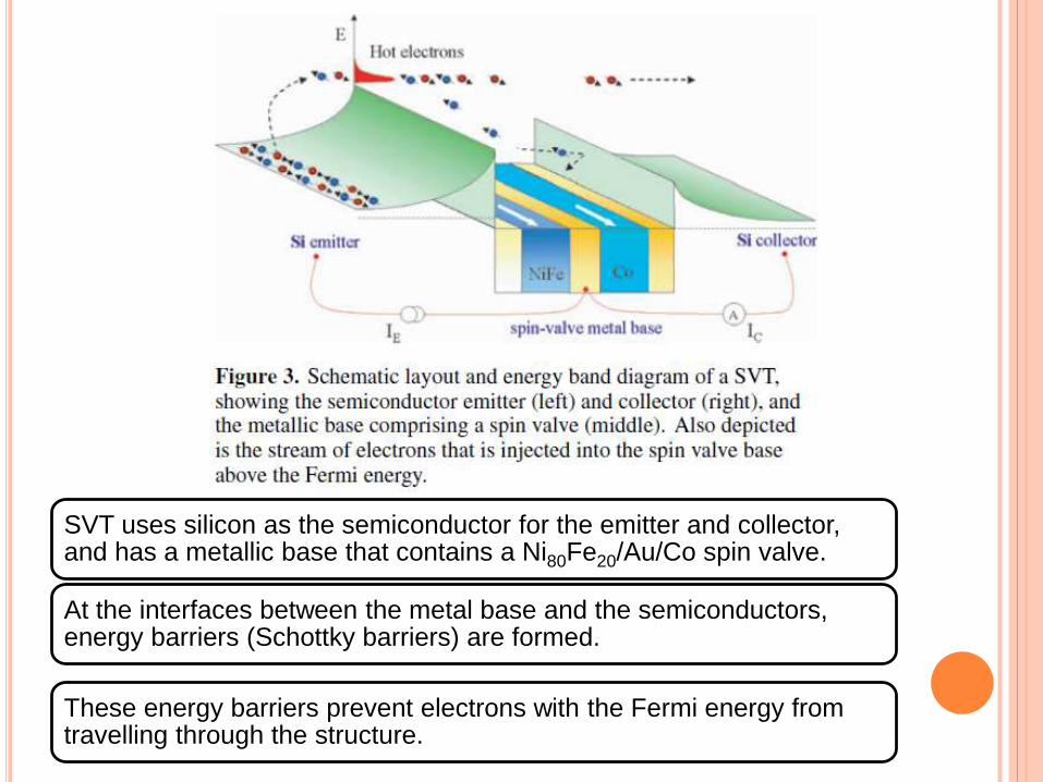
SVT uses silicon as the semiconductor for the emitter and collector, and has a metallic base that contains a Ni80Fe20/Au/Co spin valve.
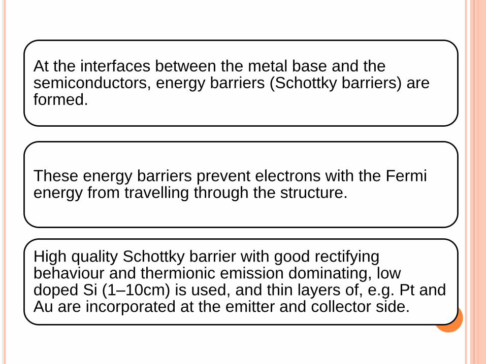
At the interfaces between the metal base and the semiconductors, energy barriers (Schottky barriers) are formed.
These energy barriers prevent electrons with the Fermi energy from travelling through the structure.
At the interfaces between the metal base and the semiconductors, energy barriers (Schottky barriers) are formed.
These energy barriers prevent electrons with the Fermi energy from travelling through the structure.
High quality Schottky barrier with good rectifying behaviour and thermionic emission dominating, low doped Si (1–10cm) is used, and thin layers of, e.g. Pt and Au are incorporated at the emitter and collector side.
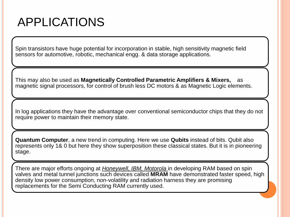
APPLICATIONS
Spin transistors have huge potential for incorporation in stable, high sensitivity magnetic field sensors for automotive, robotic, mechanical engg. & data storage applications.
This may also be used as Magnetically Controlled Parametric Amplifiers & Mixers, as magnetic signal processors, for control of brush less DC motors & as Magnetic Logic elements.
In log applications they have the advantage over conventional semiconductor chips that they do not require power to maintain their memory state.
Quantum Computer, a new trend in computing. Here we use Qubits instead of bits. Qubit also represents only 1& 0 but here they show superposition these classical states. But it is in pioneering stage.
There are major efforts ongoing at Honeywell, IBM, Motorola in developing RAM based on spin valves and metal tunnel junctions such devices called MRAM have demonstrated faster speed, high density low power consumption, non-volatility and radiation harness they are promising replacements for the Semi Conducting RAM currently used.
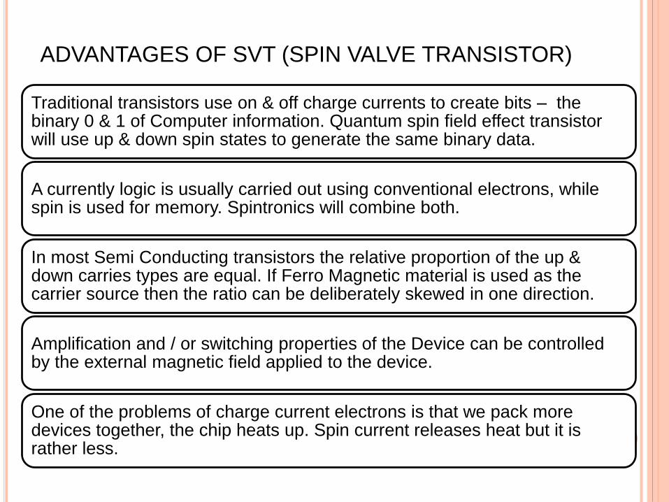
Traditional transistors use on & off charge currents to create bits – the binary 0 & 1 of Computer information. Quantum spin field effect transistor will use up & down spin states to generate the same binary data.
A currently logic is usually carried out using conventional electrons, while spin is used for memory. Spintronics will combine both.
In most Semi Conducting transistors the relative proportion of the up & down carries types are equal. If Ferro Magnetic material is used as the carrier source then the ratio can be deliberately skewed in one direction.
Amplification and / or switching properties of the Device can be controlled by the external magnetic field applied to the device.
One of the problems of charge current electrons is that we pack more devices together, the chip heats up. Spin current releases heat but it is rather less.
ADVANTAGES OF SVT (SPIN VALVE TRANSISTOR)
LIMITATIONS
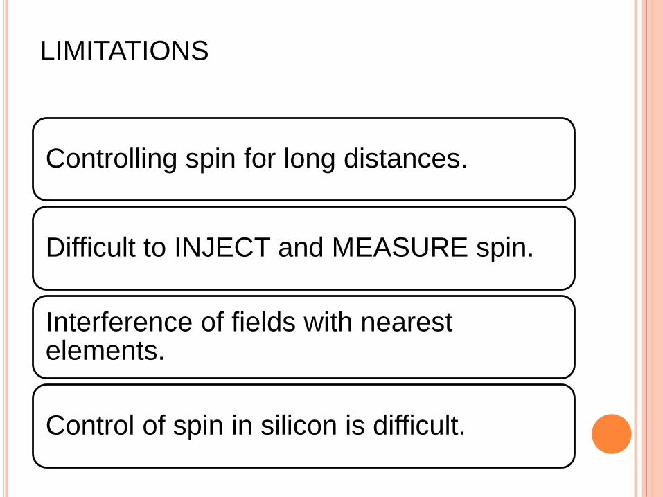
Controlling spin for long distances.
Difficult to INJECT and MEASURE spin.
Interference of fields with nearest elements.
Control of spin in silicon is difficult.
CONCLUSION
Spinvalve transistor is more versatile and more robust but it needs further fabrication methods to improve magnetic sensitivity of collector current.
The greatest hurdle for spintronic engineers may be controlling all that spin.
The key question will be whether any potential benefit of such technology will be worth the production cost.
Spin valve transistors and other spin devices will become affordable by using common metals.


![Phenalenyl-based mononuclear dysprosium complexes · 2016-11-29 · spin valve, spin transistor and spin resonator [2-5]. The fasci-Beilstein J. Nanotechnol. 2016, 7, 995–1009](https://img.pdfslide.us/doc/110x75/5e8e52ece1138157df70122e/phenalenyl-based-mononuclear-dysprosium-complexes-2016-11-29-spin-valve-spin.jpg)