Embed Size (px)
Citation preview

RF MCM Technology and Future
Microelectronics Capabilities
By Tom Terlizzi
Vice President
Aeroflex Plainview
May 10, 2011 Arlington, Va

2
Purpose
• Discuss how to navigate in the Military RF Multi Chip Module (MCM) arena using commercial technology.
• Discuss how to develop a successful strategy to
support typical Military Product Life Cycles
in conflict with Moore’s Law.
• Discuss the Future of Microelectronics Technology

3
Outline• What’s Moore’s Law & What does it mean?
• Background-COTS (Commercial Off The Shelf) : A Double Edged Sword?
• What’s RF and Where is it?
• Design and Development of a Microprocessor MCM
• Design and Development of a GaN RF MCM• • Where are we going in the future?
• Summary/ Conclusions

4
MooreMoore’’s Laws Law
• Moore's Law predicts a doubling of transistor density ~ 18 months. (Originally every year, then every two years)• Microprocessor becomes a System on Chip (SOC)
Number of Transistors

5
Percentage of Semiconductor Production Designated for Military Use By $ ValuePercentage of Semiconductor Production Designated for Military Use By $ Value
Source “Revolution in Miniature”Braun & MacDonald
(*2005 Estimate 0.3% ICE Walt Lahti** 2010 Estimate 0.3% + T.Terlizzi
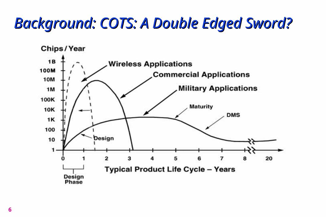
Background: COTS: A Double Edged Sword?Background: COTS: A Double Edged Sword?
2010 $304 Billion Semiconductor
Sales
~$1 Billion “Military” Sales
6
Background: COTS: A Double Edged Sword?Background: COTS: A Double Edged Sword?

76
April 15, 2002

8
The B52 will be ~90 Years Old here

9
It Used to Be That The Pilots It Used to Be That The Pilots Were Older Than The PlanesWere Older Than The Planes

Now The Planes Are Older Than The Parents And Grandparents Of The Pilots
6

11
• GOAL: Take advantage of technological advances in thecommercial and industrial component environment.
• Reduce costs at both the component and system level.• Gain access to, “Cutting Edge Technology!”• Reduce component and system lead times.
• REALITY: Accelerated exposure to componentobsolescence for major OEM’s and a new acronym DMS (Diminished Manufacturing Sources).
• COTS products Life Cycles prove to be incompatible with military program Life Cycles and funding requirements; obsolescence increases.
Background: COTS: A Double Edged Sword?Background: COTS: A Double Edged Sword?

12
Overview RFOverview RF• Radio Frequency • Radar
•Radio Detection And Ranging
• Electronic Surveillance • Communications• Countermeasures• Jamming

136

14
Design and Development of 64 Bit MIPS MCMDesign and Development of 64 Bit MIPS MCM1. Microprocessor MCM Block Diagram
2. Qualification of Key Components
3. Conservative-Robust HTCC Package Technology
4. Electrical Analysis
5. Thermal Analysis
6. Mechanical Analysis
7. Technology Insertion

15
Block Diagram of a 64 Bit MIPS MCMBlock Diagram of a 64 Bit MIPS MCM
16
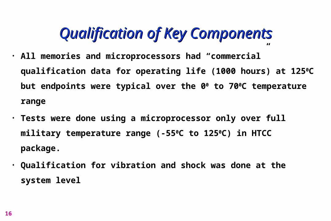
Qualification of Key ComponentsQualification of Key Components• All memories and microprocessors had “commercial”
qualification data for operating life (1000 hours) at 1250C but
endpoints were typical over the 00 to 700C temperature range
• Tests were done using a microprocessor only over full
military temperature range (-550C to 1250C) in HTCC package.
• Qualification for vibration and shock was done at the system
level
17
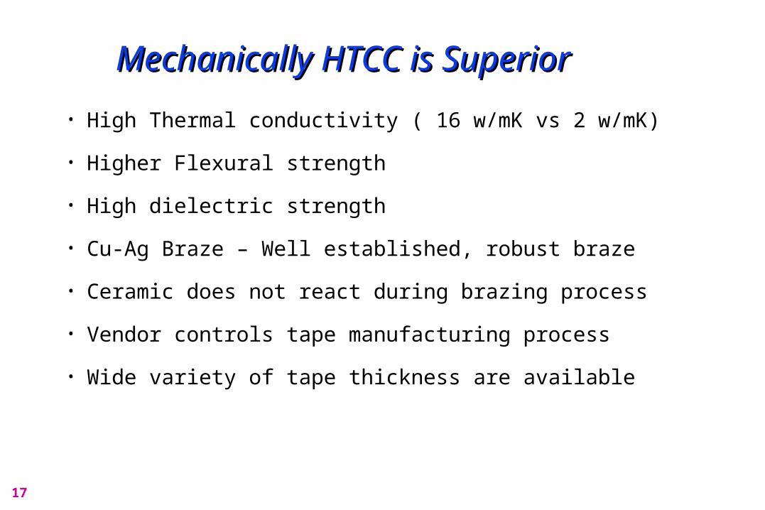
Mechanically HTCC is SuperiorMechanically HTCC is Superior• High Thermal conductivity ( 16 w/mK vs 2 w/mK)
• Higher Flexural strength
• High dielectric strength
• Cu-Ag Braze – Well established, robust braze
• Ceramic does not react during brazing process
• Vendor controls tape manufacturing process
• Wide variety of tape thickness are available

18
Package Material Selection Depends on Several FactorsPackage Material Selection Depends on Several Factors11
“Optimal” Manufacturable Package Design
Well-defined Application
Accurate Material Data
over frequency
Well-understood Process variations
TradeoffsPrice
Delivery
Performance
Manufacturing Design Guidelines
Good Simulation tools
Measurement validation
“What is the best material to use?”
SMT RF packages
LTCC MCM package
1-Slide courtesy Roy Webb - Kyocera San Diego1-Slide courtesy Roy Webb - Kyocera San Diego

19
ElectricalElectrical• Our MCM 66 Mhz clock rate with an estimated 3.0 nanoseconds.
• The system pulse rise time is 3.0 nanoseconds, the required bandwidth is 116.6 MHz.
• To reproduce the rise time with minimal distortion (<2%) would require passing the 5th harmonic or 5 x 116.6 MHz or 583.3 MHz
• The resistance of a circuit with an 8 mil line width which is two inches long can be calculated as follows:
R = ρ x l/w
where:
ρ = conductor sheet resistivity
l = length of conductor
w = width of conductor• If the sheet resistivity (ρ) is .015 ohms/□, then R = 3.75 ohms.
Solving for the maximum capacitance results in CMAX = 72.6 pf or 36.3 pf / inch or 14.28 pf / cm.
“COTS Approach to Military Microprocessor MCMs” T.Terlizzi – Military, Aerospace, Spaceand Homeland Security:
Packaging Issues and Applications IMAPS 2003

20
Electrical AnalysisElectrical Analysis

21
Thermal AnalysisThermal Analysis

22
Thermal AnalysisThermal Analysis

23
Thermal AnalysisThermal Analysis

24
Mechanical AnalysisMechanical Analysis

25
Thin Film Interposer - Thin Film Interposer - ““Picture FramePicture Frame””1 mil Aluminum wire Bonds from
R4400 Microprocessor die to the thin film interposer
1 mil Gold wires from the thin film interposer to the cofired ceramic package- two tier bonding shelf
Thin film on ceramic “picture frame”
R4400 Die

26
MIPS uP MCM MILESTONESMIPS uP MCM MILESTONES
1608-XX & 1638-XX4430SC-F10 & 4431SC-F105271/5272SC-F10 Same Footprint
•1992 1608 Initial Delivery
•1993: Introduced (256K of L2 cache)
•1994: 1st obsolescence; uP die
•1995: 2nd obsolescence; memory die
•1996: Introduced (1M of L2 Cache)•1997: 3rd obsolescence; uP die
Introduced window frame•1998: LRIP Production Orders
EOL of R4400 uP (die banking)•1999: R4430 production; Prototype of
RM5271 base part (2M of L2 Cache )•2000/2001:Continued 4430SC production
•EMD Phase of RM5271 part•2002/2010 Continued R4400 & 5271 production•2012 EOL 5272SC
280 Lead CQFP (F10)
27
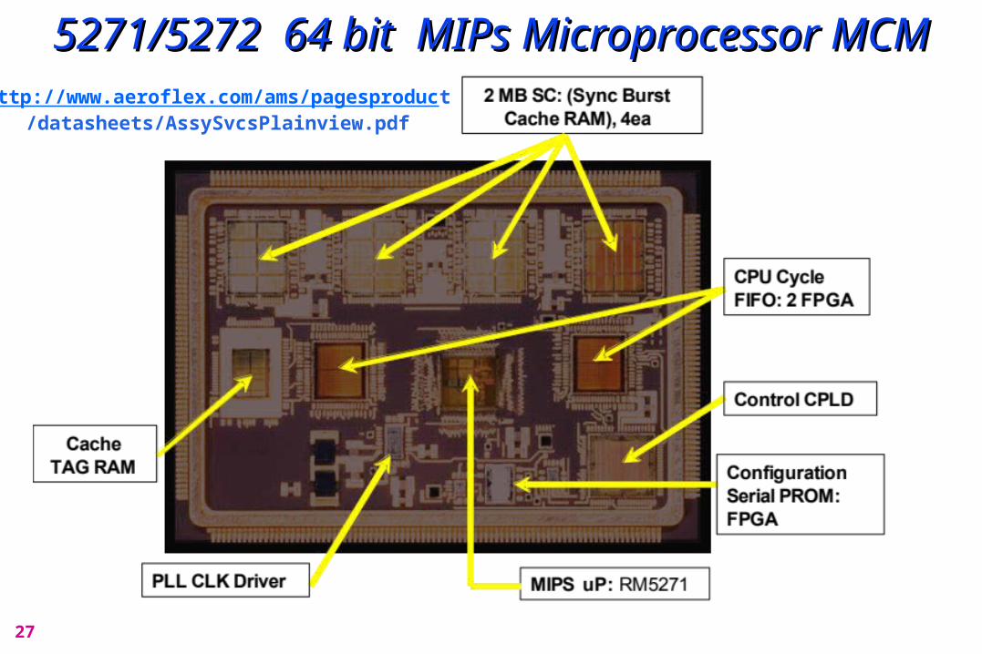
5271/5272 64 bit MIPs Microprocessor MCM5271/5272 64 bit MIPs Microprocessor MCMhttp://www.aeroflex.com/ams/pagesproduct
/datasheets/AssySvcsPlainview.pdf

28
MIPS uP Standard ProductsMIPS uP Standard Products MILESTONESMILESTONES208 Lead CQFP (F17 or F24)
5260PC 5270PC7000SC 7000ASC7965A 668 Mhz Pipeline Clock (100Mhz System Clock) Same Footprint-change core voltage
•1997: Announce MIPS Roadmap basedon QED RM52XX & RM7000 family
•1997: Ship 5260PC-F17 Prototype parts•1998: Ship 5270PC-F24 Mil-Temp parts
LRIP for Mil-Screened 5260PC-F17•1998: Ship 7000PC-F24 Mil-Temp parts•1999: Design wins for 7000SC-F17• 2000/2002: Production Phase 5260PC-F17
7000SC-F172001 •Die Bank 5260PC•2003 7000ASC 1st Design Win •2005 7965A 1st Design Win•2011 Production Phase 7965A•2012 EOL 7000SC –Maturity 7000ASC

29
Aeroflex Circuit Technology
Real Time evaluationof new processorsHigh-Rel performancefeedback Derivative design input
Utilization of advanced processor technologyEarly access to futureprocessor information
• MIPS MCM Architecture• High-Performance / High-
Reliability Screening • ( MIL-883)• High-end Integrated L2
& L3 Cache MCM Designs• Integrated Products
w/Configurable Peripherals
PMC-SIERRA• MIPS Architecture• High-end CPU Design• Core & Derivative Designs• Die Source• Technical Support• MIPS Processor Sales
Com
pete
ncie
sThe MIPS ArchitectureA Partnership for Success
• High Density Flash / SRAM / SDRAM / EEPROM MCMs
• Market & Infrastructure Development
• Sales / Service / Technical Support For MIL/Aero market
Support Partners
MIPS• MIPS Hardware / Software Design• MIPS RISC Microprocessor
Development Board Designer & Supplier
• Technical Support / Training

30
““Spinoff ProductsSpinoff Products”” STAR VII STAR VII Single Board Computer (Single Board Computer (TOP SIDE)TOP SIDE)
ACT7000SC with cavity down

31
Design and Development of Design and Development of GaN Wide Band Amplifier for Space ApplicationsGaN Wide Band Amplifier for Space Applications1. Amplifier Block Diagram
2. Qualification of Key Components
3. Conservative-Robust Package Technology
4. Electrical Analysis
5. Thermal Analysis
6. Mechanical Analysis

32
Block Diagram & Outline DrawingBlock Diagram & Outline Drawing

33
Broadband GaN Amplifier PA020180-3922Broadband GaN Amplifier PA020180-3922
• 2GHz to18GHz 8 Watts• Psat 39 dBm
• 23 dB & 35dB typical Gain • Compact size • 2.7” x 1.6” x 0.42”

34
Aeroflex in SpaceAeroflex in Space• Aeroflex Plainview, Inc is a MIL-PRF-38534 Class “K”
qualified manufacturer, as well ISO-9001-2000 certified with AS9100-2004, Rev B performing all manufacturing, screening and element evaluation in accordance with the Mil-Performance requirements on standard and custom products.
• Aeroflex has manufactured and delivered thousands of Class “K” Level Space Application Multi-Chip Modules (MCMs), Hybrids, ASICs and MMICs to major commercial and military satellite OEMs such as Boeing Satellite Systems (BSS), Northrop Grumman Aerospace Systems (NGAS), Space Systems/ Loral (SS/L), Honeywell and Lockheed Martin Space Systems Division (LMSSD)
• Aeroflex has >25 years expertise in designing, testing and screening of Radiation Hardened RF components.

35
Space Level Class S Cree GaN Die screening & QualificationSpace Level Class S Cree GaN Die screening & QualificationMIL-PRF-38534E APPENDIX C
1/ MIL-PRF-38534 methods

36
Cree GaN die Space Qualification ProcessCree GaN die Space Qualification ProcessWafer Fabrication in done in a certified clean room (Sub Group 1)Wafer Fabrication in done in a certified clean room (Sub Group 1)
Fabricated wafers are 100% DC testedFabricated wafers are 100% DC tested
CreeCree’’s internal procedures for ESD and wafer handling are strictly followed. The tested s internal procedures for ESD and wafer handling are strictly followed. The tested wafer is diced (Sub Group 1)wafer is diced (Sub Group 1)
Each die is visually inspected 100% to ensure conformance to Each die is visually inspected 100% to ensure conformance to the applicable die related requirements of MIL-STD-883 the applicable die related requirements of MIL-STD-883 Method 2010 condition A=Class K: Internal visual for Method 2010 condition A=Class K: Internal visual for
Multichip Modules (MCM) (Sub Group 2)Multichip Modules (MCM) (Sub Group 2)
Test Fixture Test Fixture Assembly:Assembly:
(sub Group 3 and 4)(sub Group 3 and 4)
Wire bond Wire bond evaluationevaluation
(Sub Group 5)(Sub Group 5)
SEM (Scanning Electron Microscopy)SEM (Scanning Electron Microscopy)
A SEM inspection is performed to provide a A SEM inspection is performed to provide a means of judging the quality of the device means of judging the quality of the device metallization. The test is made in accordance metallization. The test is made in accordance with MIL-STD-883 method 2018 or 2077 with MIL-STD-883 method 2018 or 2077 (Sub Group 6)(Sub Group 6)

37
Cree Quality and ReliabilityCree Quality and Reliability

38
Cree Quality and ReliabilityCree Quality and Reliability

39
GaN Radiation Testing (Yale University)GaN Radiation Testing (Yale University)

40
GaN Radiation Testing SetupGaN Radiation Testing Setup

41
GaN Radiation Testing ResultsGaN Radiation Testing Results
200 Mrads of Protons had no effect – switching 20 V 0.1 AmpParts still activated after 7 months

42
GaN Radiation Testing ResultsGaN Radiation Testing Results

43
GaN Radiation Testing ResultsGaN Radiation Testing Results

44
NASA Radiation Testing GaN on SiCNASA Radiation Testing GaN on SiC
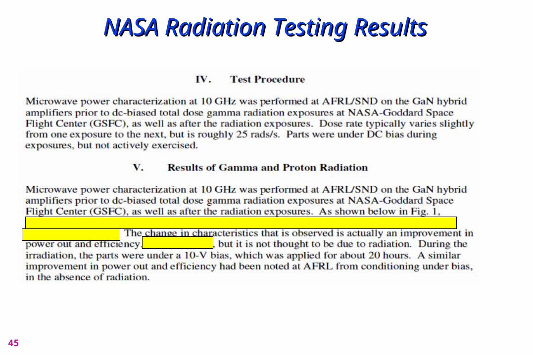
45
NASA Radiation Testing ResultsNASA Radiation Testing Results

46
NASA Radiation Testing ResultsNASA Radiation Testing Results

47
ElectricalElectrical

48
Cree ThermalCree Thermal
49
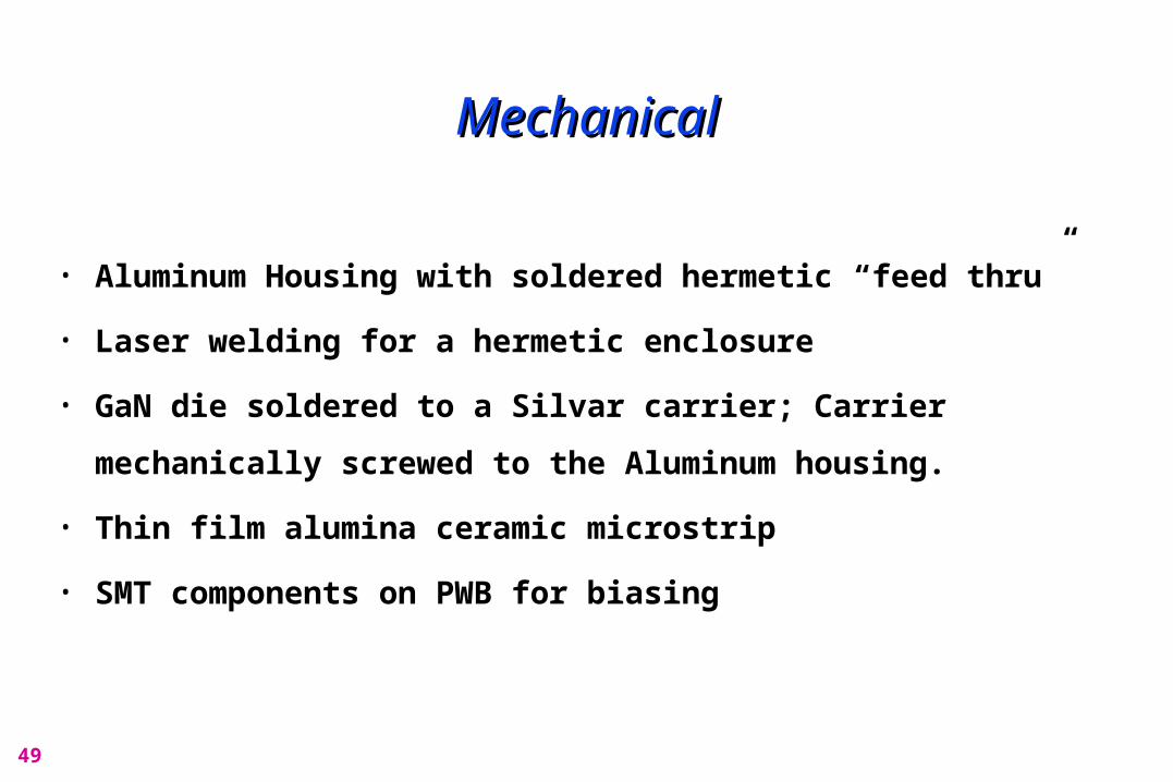
MechanicalMechanical
• Aluminum Housing with soldered hermetic “feed thru”
• Laser welding for a hermetic enclosure
• GaN die soldered to a Silvar carrier; Carrier mechanically
screwed to the Aluminum housing.
• Thin film alumina ceramic microstrip
• SMT components on PWB for biasing
50
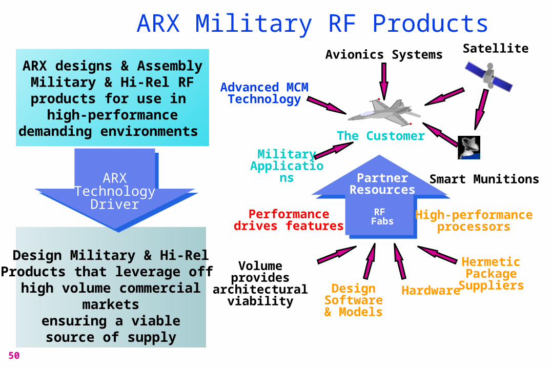
ARX designs & AssemblyMilitary & Hi-Rel RFproducts for use in high-performance
demanding environments
ARX Military RF Products
Volume providesarchitectural
viability
Design Military & Hi-RelProducts that leverage off high volume commercial
marketsensuring a viablesource of supply
Design Software & Models
Hardware
HermeticPackage Suppliers
MilitaryApplications
SatelliteAvionics Systems
The Customer
Advanced MCM Technology
Performancedrives features
Smart Munitions
High-performanceprocessors
ARXTechnology
Driver
PartnerResources
RF Fabs

51
Where are we going?Where are we going?• New RF Integrated Circuit Technologies will lead to
• more integration• smaller, lightweight, more reliable components
• Digital and Analog RF functions are merging• Generation of New Advanced Semiconductor Materials • Improvement in Silicon RF power amplifiers• Improvements in GaAs technology• 3-D Packaging – TSV “Thru Silicon Via”• COB Chip on Board• RF MEMs switches and oscillators• RF friendly Plastic Packaging • Low temperature ALD (Atomic Layer Deposition)

52
Cell Phone TechnologyCell Phone Technology
Motorola Atrix 4G Teardown http://www.ifixit.com/Teardown/
Motorola-Atrix-4G-Teardown/4964/1
53
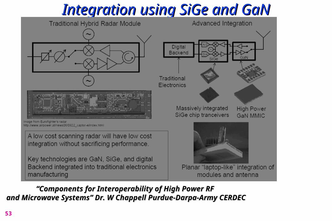
Integration using SiGe and GaNIntegration using SiGe and GaN
““Components for Interoperability of High Power RF Components for Interoperability of High Power RF and Microwave Systemsand Microwave Systems”” Dr. W Chappell Purdue-Darpa-Army CERDEC Dr. W Chappell Purdue-Darpa-Army CERDEC

54
Commercial GPS ReceiverCommercial GPS Receiver

55
International Technology Roadmap for International Technology Roadmap for Semiconductors (ITRS)Semiconductors (ITRS)
Year
Parameter
2003 2004 2005 2008 2011 2014
Technology(nm) 120 110 100 70 50 35
# of Transistors 95.2M 145M 190M 539M 1,523M 4,308M
Clock Frequency 1,724 MHz 1,857 MHz 2,000 MHz 2,500 MHz 3,000 MHz 3,600 MHz
Chip Area (mm2) 372 372 408 468 536 615
Wiring Levels 8 8 8-9 9 9-10 10
Pitch(L/I/G)(nm) 330/420/690 295/375/620 265/340/560 185/240/390 130/165/275 95/115/190
A/R (L/I/G) 1.6/2.2/2.8 1.6/2.3/2.8 1.7/2.4/2.8 1.9/2.5/2.9 2.1/2.7/3.0 2.3/2.9/3.1
Dielectric Const. 2.2-2.7 2.2-2.7 1.6-2.2 1.5 <1.5 <1.5
This data is from the ITRS Roadmap on interconnects
http://www.itrs.net/

56
Systems on Chip (SOC)Systems on Chip (SOC)
57
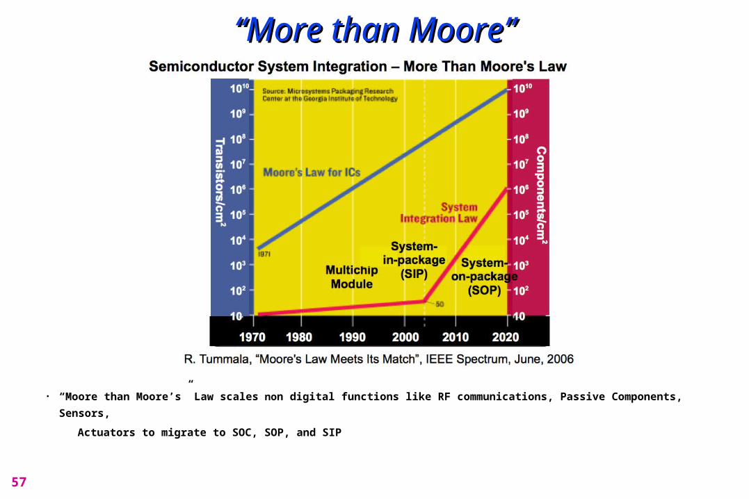
““More than MooreMore than Moore””
• “Moore than Moore’s” Law scales non digital functions like RF communications, Passive Components, Sensors,
Actuators to migrate to SOC, SOP, and SIP

58
DefinitionsDefinitions
http://www.chipscalereview.com/issues/0104/article.php?type=feature&article=f8

59
System on Package (SOP)System on Package (SOP)
“Going Vertical from More than More to even Mo(o)re” Dr. M SwaminathanGa. Tech.

60
Aeroflex Chip on Board (COB)Aeroflex Chip on Board (COB)
DC-DC Plug-and-Play Low-Voltage Power Supply, Non-RadHard +28V Input. Output: +5V, +3.3V, +2.5V, 70W – ACT8616
http://www.aeroflex.com/ams/pagesproduct/datasheets/AssySvcsPlainview.pdf

61
Advantages of GaN Semiconductor MaterialAdvantages of GaN Semiconductor Material• GaN is the most promising semiconductor material for microwave
power devices for space applications
• Higher power density – demonstrated 10W/mm @ X-band• High added power efficiency – 60% @ X- band• Broadband response - Measured response from 1-20GHz• High Breakdown voltage (3.4eV) – 5X GaAs (for
space applications - better derating criteria)• Higher operating junction temperature (up to 275ºC) with 2.2M hours
operating life is 225ºC• Bias Voltage of up to 50V (+28V)• Excellent Radiation Tolerance

62
Advantages of GaN Semiconductor Advantages of GaN Semiconductor MaterialMaterial

63
3-D Packaging3-D Packaging
1950’s Project Tinker ToyMicro Module
1960’s
Cord Wood Modules
TSV

64
SummarySummary• COTS is here to stay…The definition continues to change• The markets for semiconductor devices are driven
exclusively by commercial and consumer industriesNew product are being designed to perform in commercial or industrial temperature ranges only
• The military will no longer have dedicated componentsources…Military spending accounts for only 0.3% of total US semiconductor sales in 2010-2015 time period
• Component obsolescence presents a serious challengeto both Component Manufacturers and OEM’s
• Component obsolescence issues will only increase • i.e. counterfeit parts

65
ConclusionsConclusions • COTS is here to stay...• “Military RF MCM,” suppliers can develop a successful
strategy to support typical military Product Life Cycles. • Component suppliers must be flexibleflexible and able to adapt:
the market is constantly changing…New IC sources and new semiconductor technologyDie ShrinksEvolving Packaging Technology“Alphabet Soup” of new fabless companies
With “A Proactive Approach” to develop ROBUST technology a RF MCM Suppliers can be successful in the COTS world

66
YOU’RE NOT GETTING OLDER YOU’RE GETTING BETTER

67
“You’re not getting older,you’re getting better”