Embed Size (px)
Citation preview
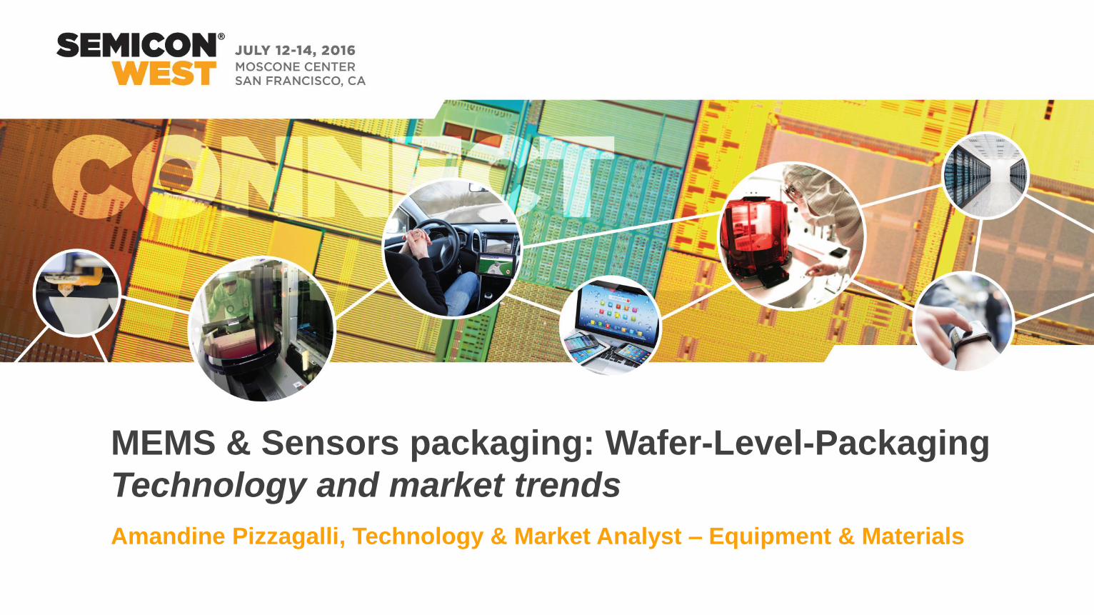
MEMS & Sensors packaging: Wafer-Level-Packaging
Technology and market trends
Amandine Pizzagalli, Technology & Market Analyst – Equipment & Materials
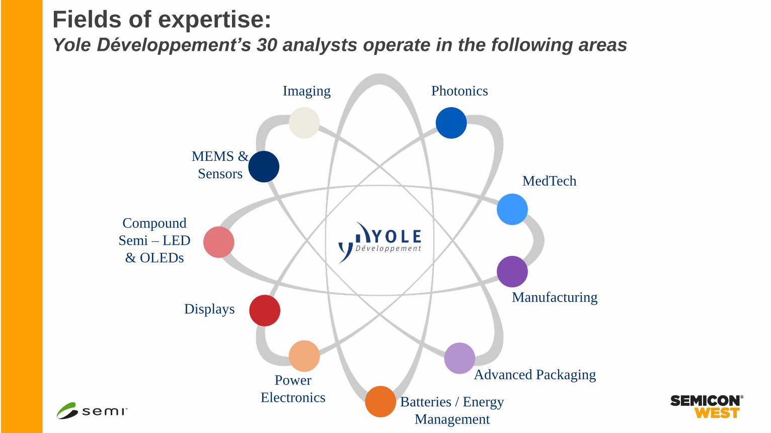
Fields of expertise:Yole Développement’s 30 analysts operate in the following areas
MEMS &
Sensors
Displays
Compound
Semi – LED
& OLEDs
Imaging Photonics
MedTech
Manufacturing
Advanced Packaging
Batteries / Energy
Management
Power
Electronics
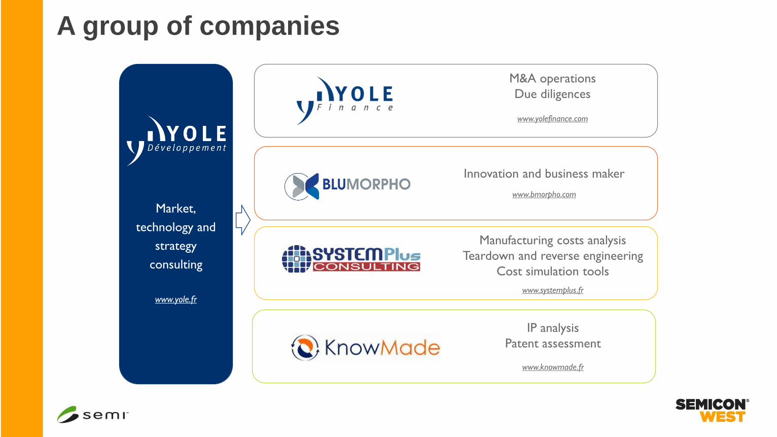
A group of companies
Market,
technology and
strategy
consulting
www.yole.fr
M&A operations
Due diligences
www.yolefinance.com
Innovation and business maker
www.bmorpho.com
Manufacturing costs analysis
Teardown and reverse engineering
Cost simulation tools
www.systemplus.fr
IP analysis
Patent assessment
www.knowmade.fr

Outline of the presentation
• Market trends & MEMS sensors
• Focus on Packaging technologies for MEMS
devices
• Conclusion

The 5 senses and many more: MEMS, sensors
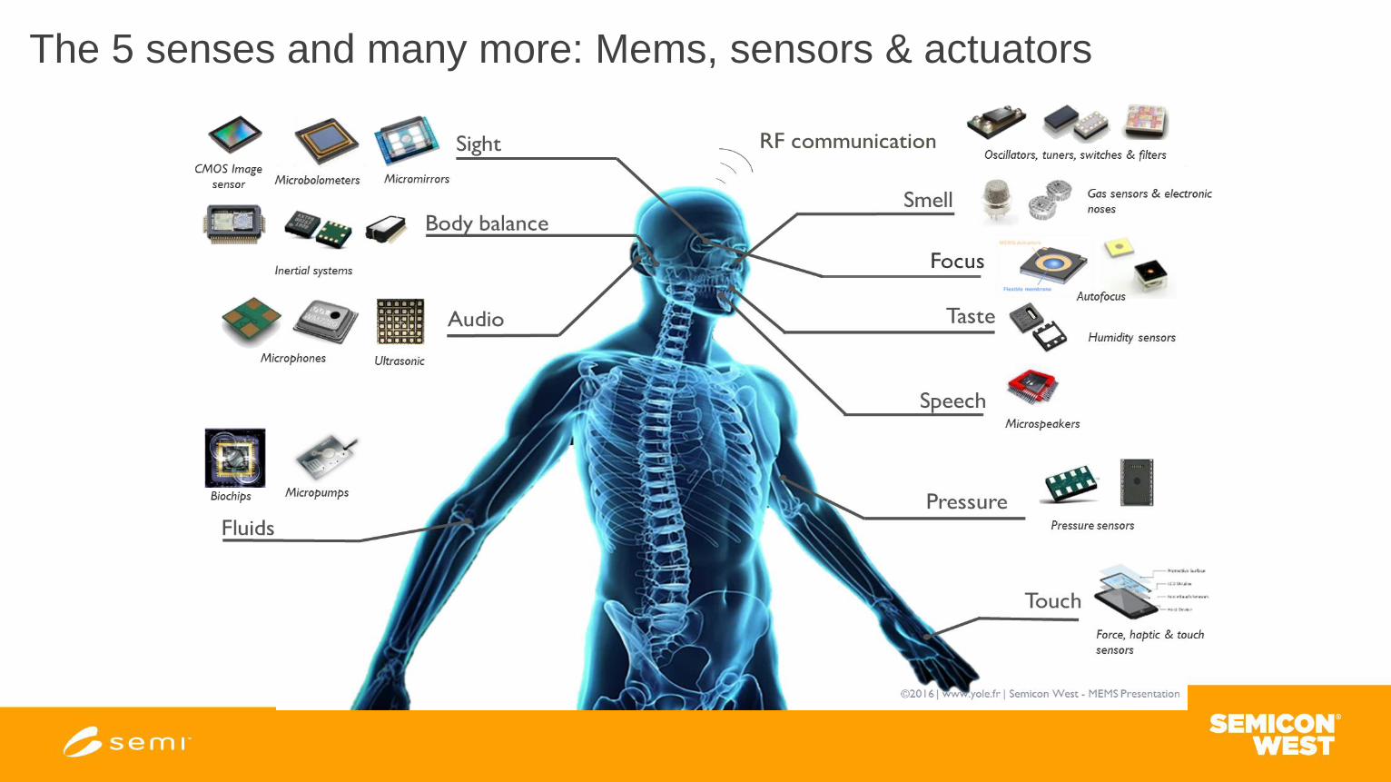
The 5 senses and many more: Mems, sensors & actuators
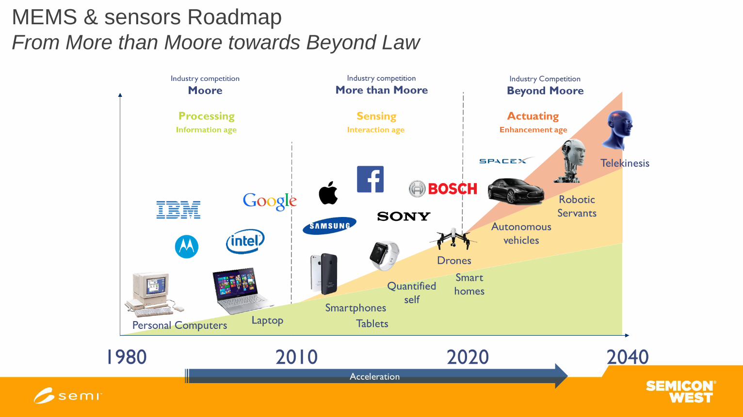
MEMS & sensors RoadmapFrom More than Moore towards Beyond Law
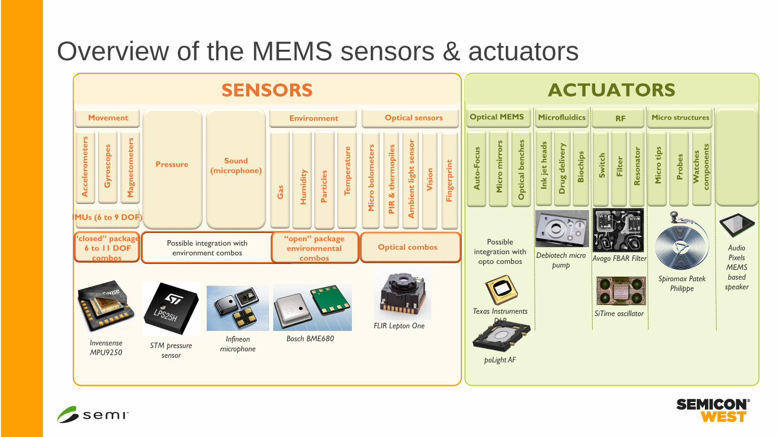
Overview of the MEMS sensors & actuators
ACTUATORSSENSORS
Pressure Sound
(microphone)
Environment Optical sensors
Dru
g d
elivery
Microfluidics
Ink j
et
head
s
Au
to-F
ocu
s
Mic
ro m
irro
rs
RFOptical MEMS Micro structures
Parti
cle
s
Hu
mid
ity
Movement
Gas
Magn
eto
mete
rs
IMUs (6 to 9 DOF)
Accele
rom
ete
rs
Gyro
sco
pes
Tem
pera
ture
Op
tical b
en
ch
es
Mic
ro t
ips
Pro
bes
Watc
hes
co
mp
on
en
ts
PIR
& t
herm
op
iles
Mic
ro b
olo
mete
rs
Sw
itch
Filte
r
Bosch BME680
FLIR Lepton One
Infineon
microphoneSTM pressure
sensor
Invensense
MPU9250
Debiotech micro
pump
Texas Instruments
DLP
Avago FBAR Filter
Spiromax Patek
Philippe
Audio
Pixels
MEMS
based
speaker
Reso
nato
r
Bio
ch
ips
poLight AF
SiTime oscillator
Am
bie
nt
ligh
t se
nso
r
Fin
gerp
rin
t
Vis
ion
Optical combos“open” package
environmental
combos
“closed” package
6 to 11 DOF
combos
Possible integration with
environment combos
Possible
integration with
opto combos
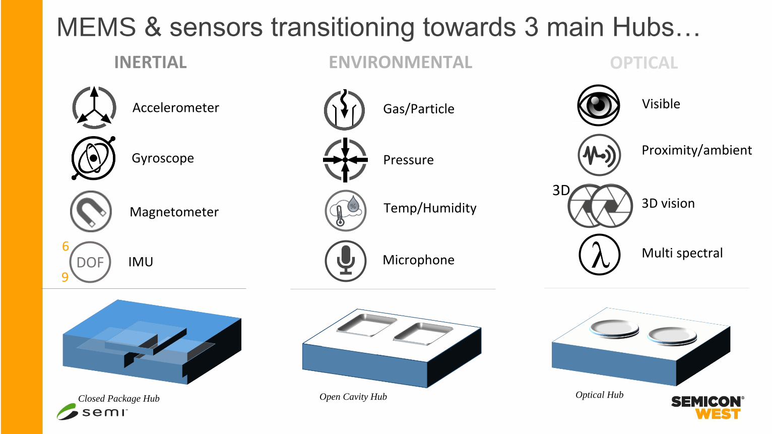
MEMS & sensors transitioning towards 3 main Hubs…
Closed Package Hub
Accelerometer
Gyroscope
Magnetometer
INERTIAL
DOF6
9IMU
ENVIRONMENTAL
Open Cavity Hub
Gas/Particle
Pressure
Temp/Humidity
Microphone
OPTICAL
Optical Hub
Visible
3D vision
Multi spectral
3D
Proximity/ambient
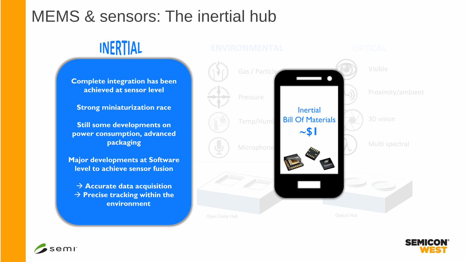
MEMS & sensors: The inertial hub
Closed Package Hub
Accelerometer
Gyroscope
Magnetometer
DOF6
9IMU
ENVIRONMENTAL
Open Cavity Hub
Gas / Particle
Pressure
Temp/Humidity
Microphone
OPTICAL
Optical Hub
Visible
3D vision
Multi spectral
3D
Proximity/ambient
Complete integration has been
achieved at sensor level
Strong miniaturization race
Still some developments on
power consumption, advanced
packaging
Major developments at Software
level to achieve sensor fusion
Accurate data acquisition
Precise tracking within the
environment
Inertial
Bill Of Materials
$1
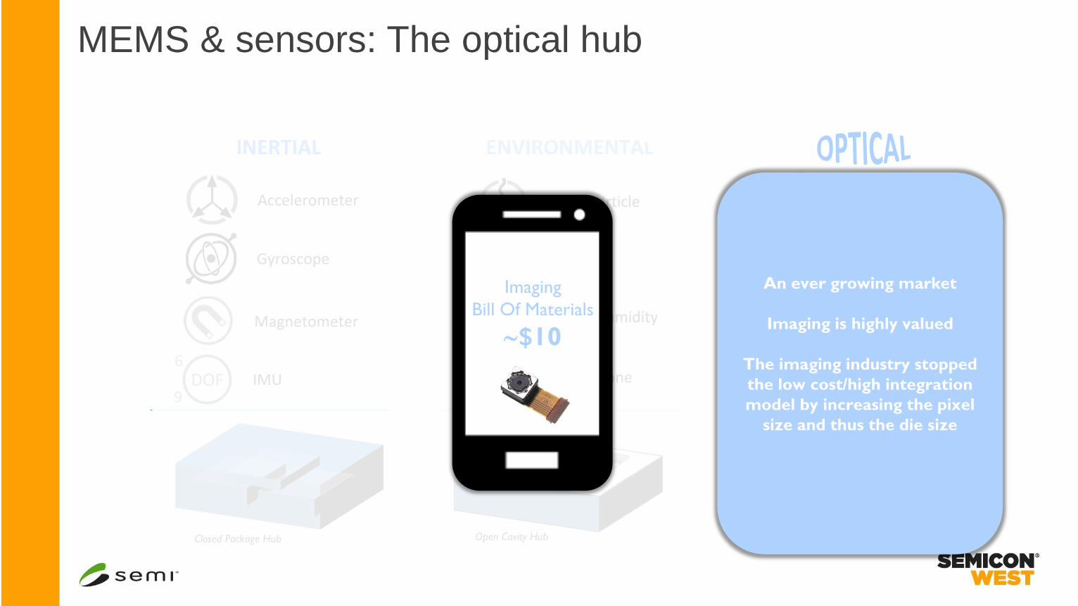
MEMS & sensors: The optical hub
Closed Package Hub
Accelerometer
Gyroscope
Magnetometer
INERTIAL
DOF6
9IMU
ENVIRONMENTAL
Open Cavity Hub
Gas / Particle
Pressure
Temp/Humidity
Microphone
Optical Hub
Visible
3D vision
Multi spectral
3D
Proximity/ambient
An ever growing market
Imaging is highly valued
The imaging industry stopped
the low cost/high integration
model by increasing the pixel
size and thus the die size
Imaging
Bill Of Materials
$10

MEMS & sensors: The environmental hub
Closed Package Hub
Accelerometer
Gyroscope
Magnetometer
INERTIAL
DOF6
9IMU
Open Cavity Hub
Gas / Particle
Pressure
Temp/Humidity
Microphone
OPTICAL
Optical Hub
Visible
3D vision
Multi spectral
3D
Proximity/ambientInteresting way for the
MEMS industry to gain value:
More integration at
environmental level
Pressure + Microphone
Add Particles & Gas
detection (market pull)
Environmental
Bill Of Materials
$1.50
Environmental
Bill Of Materials
$0.70
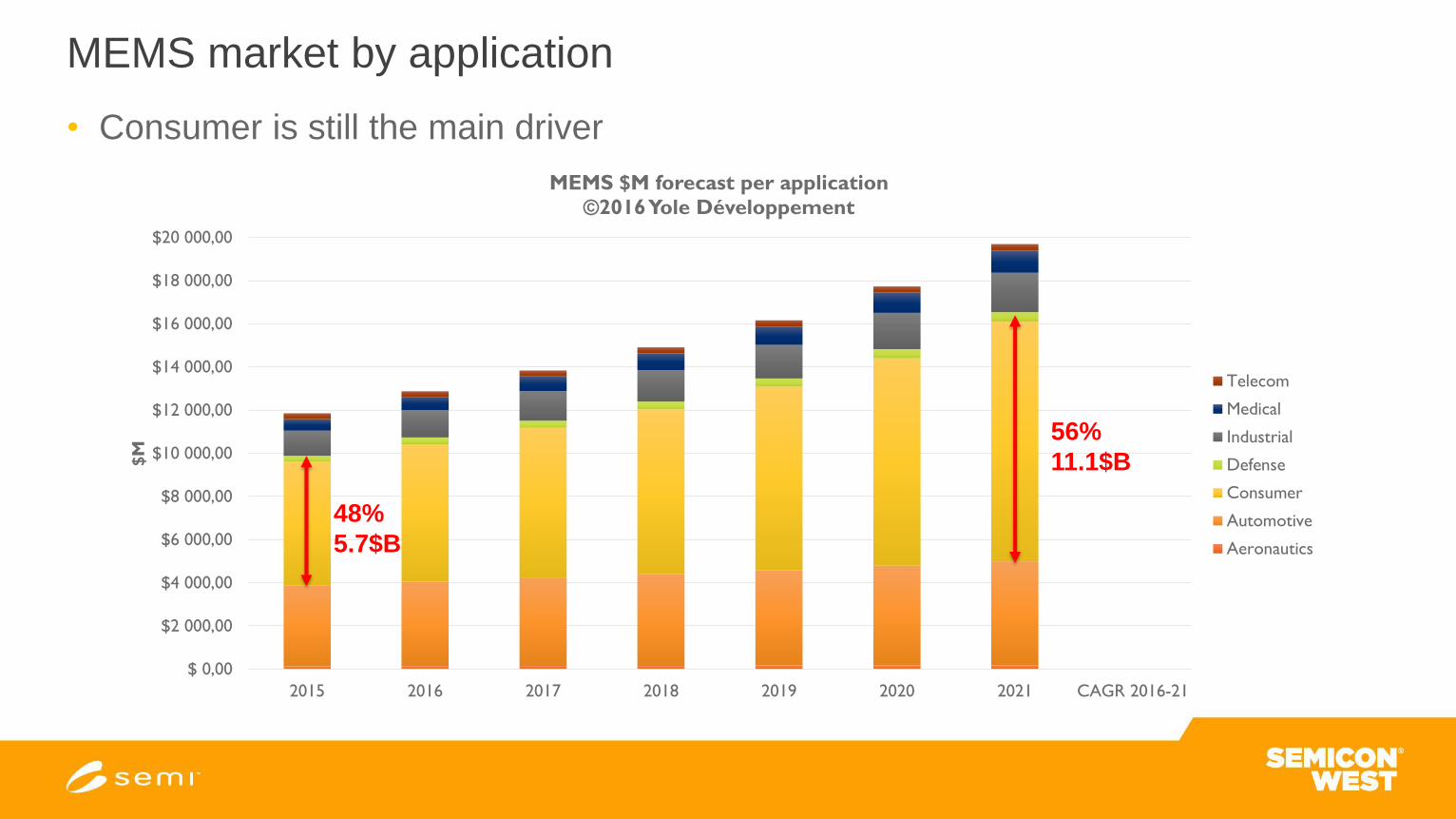
MEMS market by application
• Consumer is still the main driver
$ 0,00
$2 000,00
$4 000,00
$6 000,00
$8 000,00
$10 000,00
$12 000,00
$14 000,00
$16 000,00
$18 000,00
$20 000,00
2015 2016 2017 2018 2019 2020 2021 CAGR 2016-21
$M
MEMS $M forecast per application
©2016 Yole Développement
Telecom
Medical
Industrial
Defense
Consumer
Automotive
Aeronautics
48%
5.7$B
56%
11.1$B
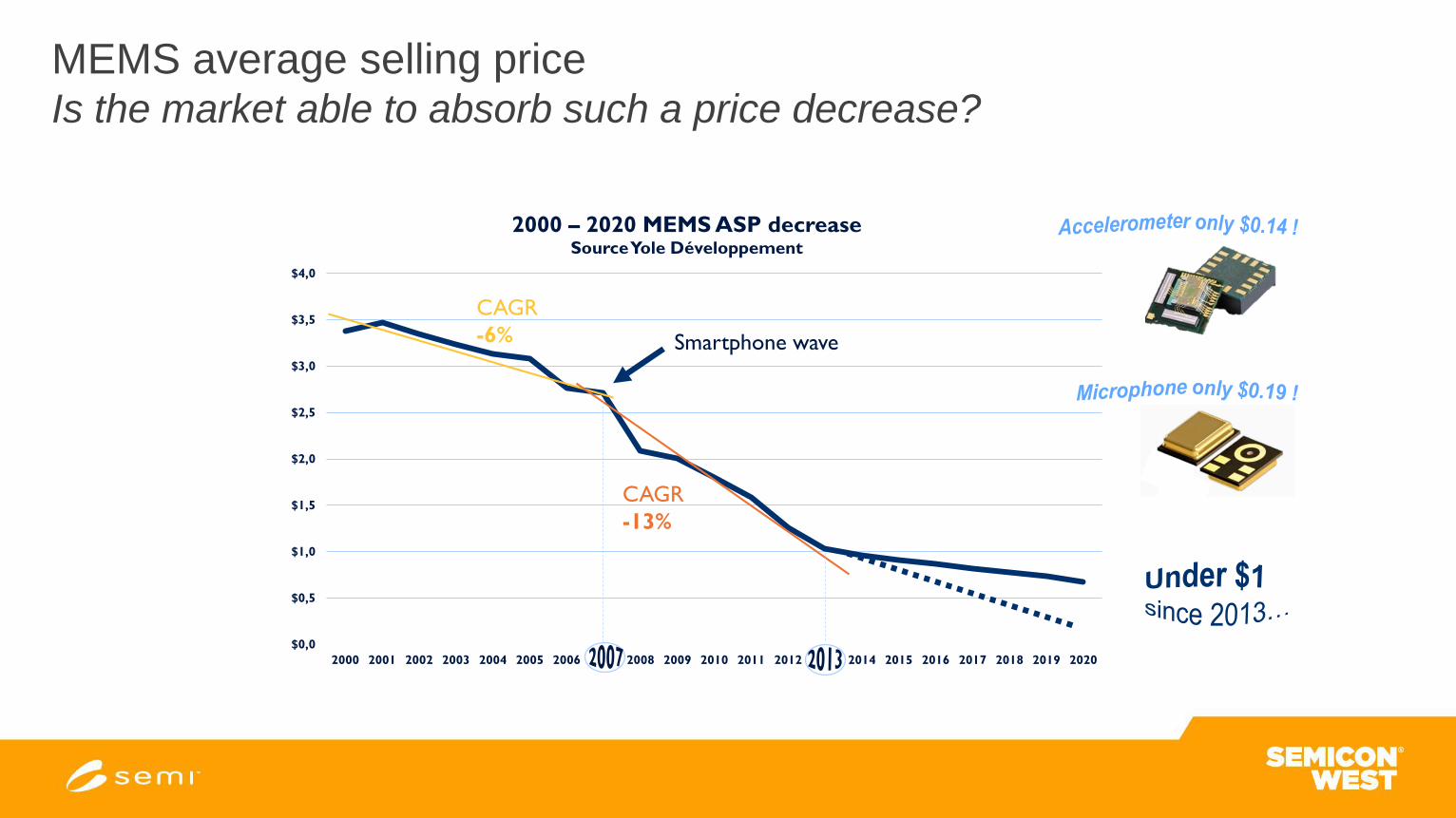
MEMS average selling priceIs the market able to absorb such a price decrease?
$0,0
$0,5
$1,0
$1,5
$2,0
$2,5
$3,0
$3,5
$4,0
2000 2001 2002 2003 2004 2005 2006 2007 2008 2009 2010 2011 2012 2013 2014 2015 2016 2017 2018 2019 2020
2000 – 2020 MEMS ASP decreaseSource Yole Développement
Smartphone wave
CAGR
-6%
CAGR
-13%

New MEMS challenges
• Yesterday, the main MEMS challenges were size decrease, which in turn led to price decrease then volume growth.
• Today, trends are different. They are: importance of user case (start with the definition of an application), fusion different
sensors with software and power decrease (which paradoxically is linked to an chip size increase because of the ASIC)
Yesterday
ASP decreaseConsumer
volume
Size decrease
2016, a new virtuous cycle?
Power
consumption
decrease
Importance
for user case
Sensor fusion,
software & more
features
Mobiles have to survive for long
periods on battery power while
interacting with environment (voice
calls, Wi-Fi, Bluetooth, GPS, sensors
…).
Start with applications, and work
downwards to the chips needed to
support them.
Less silicon, more brain.
Start with more intelligence!
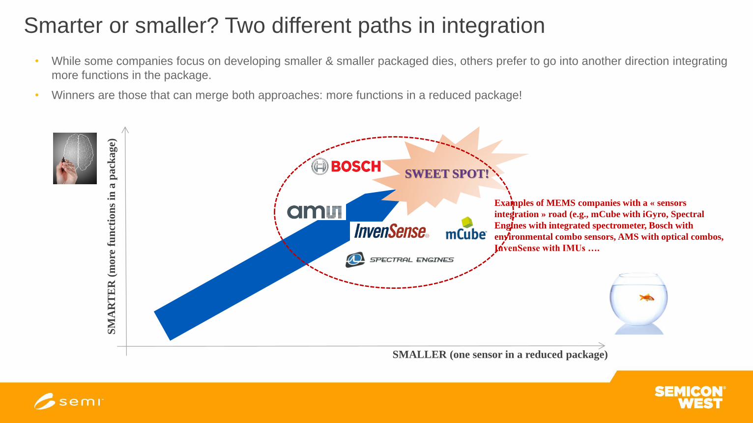
Smarter or smaller? Two different paths in integration
• While some companies focus on developing smaller & smaller packaged dies, others prefer to go into another direction integrating
more functions in the package.
• Winners are those that can merge both approaches: more functions in a reduced package!
SMALLER (one sensor in a reduced package)
SM
AR
TE
R (
more
fu
nct
ion
s in
a p
ack
age)
SWEET SPOT!
Examples of MEMS companies with a « sensors
integration » road (e.g., mCube with iGyro, Spectral
Engines with integrated spectrometer, Bosch with
environmental combo sensors, AMS with optical combos,
InvenSense with IMUs ….
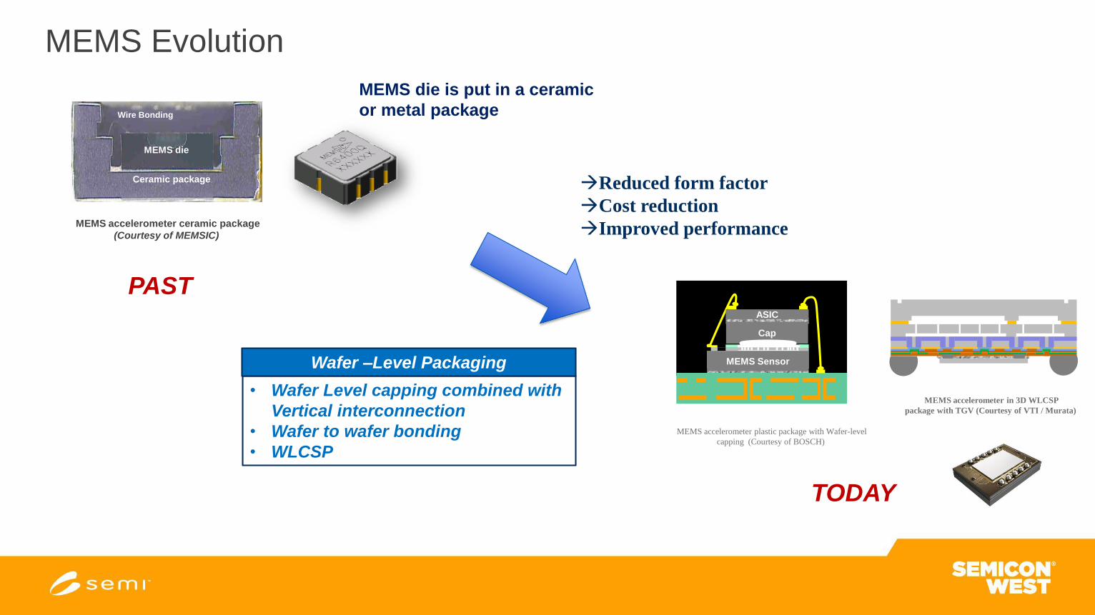
MEMS Evolution
MEMS die
Ceramic package
Wire Bonding
MEMS accelerometer ceramic package
(Courtesy of MEMSIC)
ASIC
Cap
MEMS Sensor
MEMS accelerometer plastic package with Wafer-level
capping (Courtesy of BOSCH)
MEMS accelerometer in 3D WLCSP
package with TGV (Courtesy of VTI / Murata)
PAST
TODAY
• Wafer Level capping combined with
Vertical interconnection
• Wafer to wafer bonding
• WLCSP
MEMS die is put in a ceramic
or metal package
Wafer –Level Packaging
Reduced form factor
Cost reduction
Improved performance
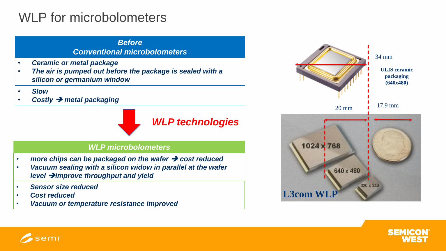
WLP for microbolometers
L3com WLP
17.9 mm
34 mm
ULIS ceramic
packaging
(640x480)
20 mm
Before
Conventional microbolometers
• Ceramic or metal package
• The air is pumped out before the package is sealed with a
silicon or germanium window
• Slow
• Costly metal packaging
WLP microbolometers
• more chips can be packaged on the wafer cost reduced
• Vacuum sealing with a silicon widow in parallel at the wafer
level improve throughput and yield
• Sensor size reduced
• Cost reduced
• Vacuum or temperature resistance improved
WLP technologies
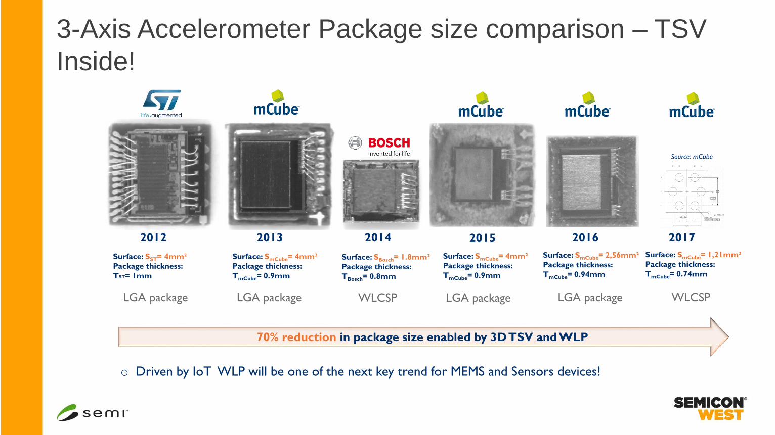
3-Axis Accelerometer Package size comparison – TSV
Inside!
Surface: SST= 4mm²
Package thickness:
TST= 1mm
Surface: SmCube= 4mm²
Package thickness:
TmCube= 0.9mm
Surface: SBosch= 1.8mm²
Package thickness:
TBosch= 0.8mm
2013 20142012 2015 2016 2017
Surface: SmCube= 4mm²
Package thickness:
TmCube= 0.9mm
Surface: SmCube= 2,56mm²
Package thickness:
TmCube= 0.94mm
Surface: SmCube= 1,21mm²
Package thickness:
TmCube= 0.74mm
LGA package LGA package LGA packageWLCSP WLCSPLGA package
o Driven by IoT WLP will be one of the next key trend for MEMS and Sensors devices!
Source: mCube
70% reduction in package size enabled by 3D TSV and WLP
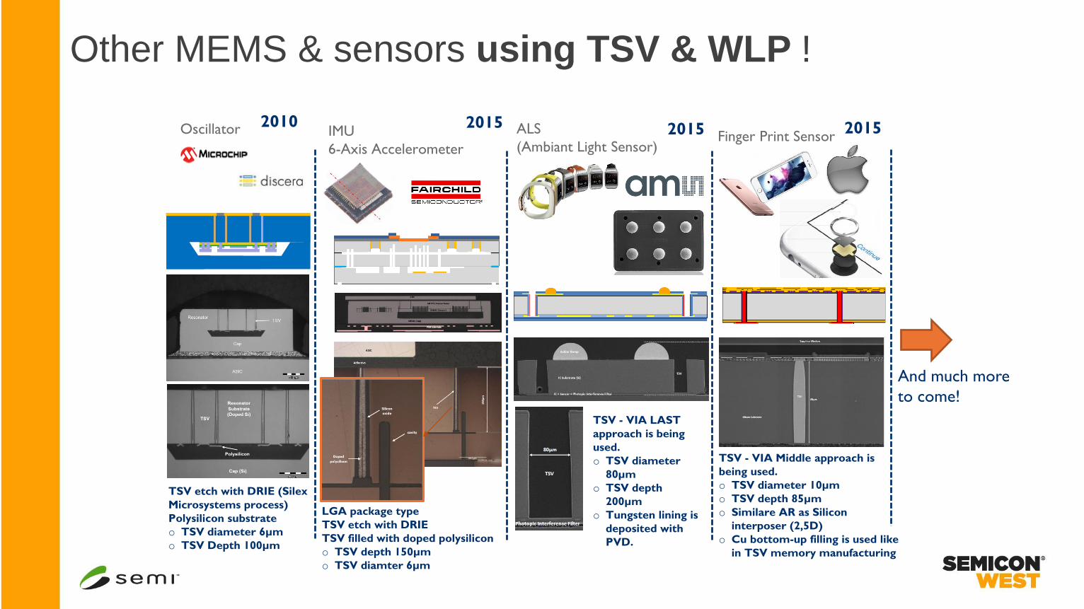
Other MEMS & sensors using TSV & WLP !
ALS
(Ambiant Light Sensor)IMU
6-Axis Accelerometer
2015Oscillator
And much more
to come!
TSV etch with DRIE (Silex
Microsystems process)
Polysilicon substrate
o TSV diameter 6µm
o TSV Depth 100µm
LGA package type
TSV etch with DRIE
TSV filled with doped polysilicon
o TSV depth 150µm
o TSV diamter 6µm
TSV - VIA LAST
approach is being
used.
o TSV diameter
80µm
o TSV depth
200µm
o Tungsten lining is
deposited with
PVD.
TSV - VIA Middle approach is
being used.
o TSV diameter 10µm
o TSV depth 85µm
o Similare AR as Silicon
interposer (2,5D)
o Cu bottom-up filling is used like
in TSV memory manufacturing
2015 20152010Finger Print Sensor
Conclusions
Conclusions and future perspectives
• MEMS & sensors are facing a strong demand driven by the consumer and
cost pressure
• Wafer Level Packaging significantly reduces the sensor size and has an
impact on the cost and performance
• New MEMS architectures are more and more required to achieve higher
features and functionalities in smaller footprint
• Therefore, WLP and TSV are the key packaging technologies enabling to
achieve innovative functions, higher performances as well as cost effective
integration