Embed Size (px)
Citation preview
Dr. S.Meenatchi Sundaram, Department of Instrumentation & Control Engineering, MIT, Manipal
ICE 4010: MICRO ELECTRO MECHANICAL SYSTEMS (MEMS)
Lecture #02
History & Characteristics of MEMS
Dr. S. Meenatchi Sundaram
Email: [email protected]
1
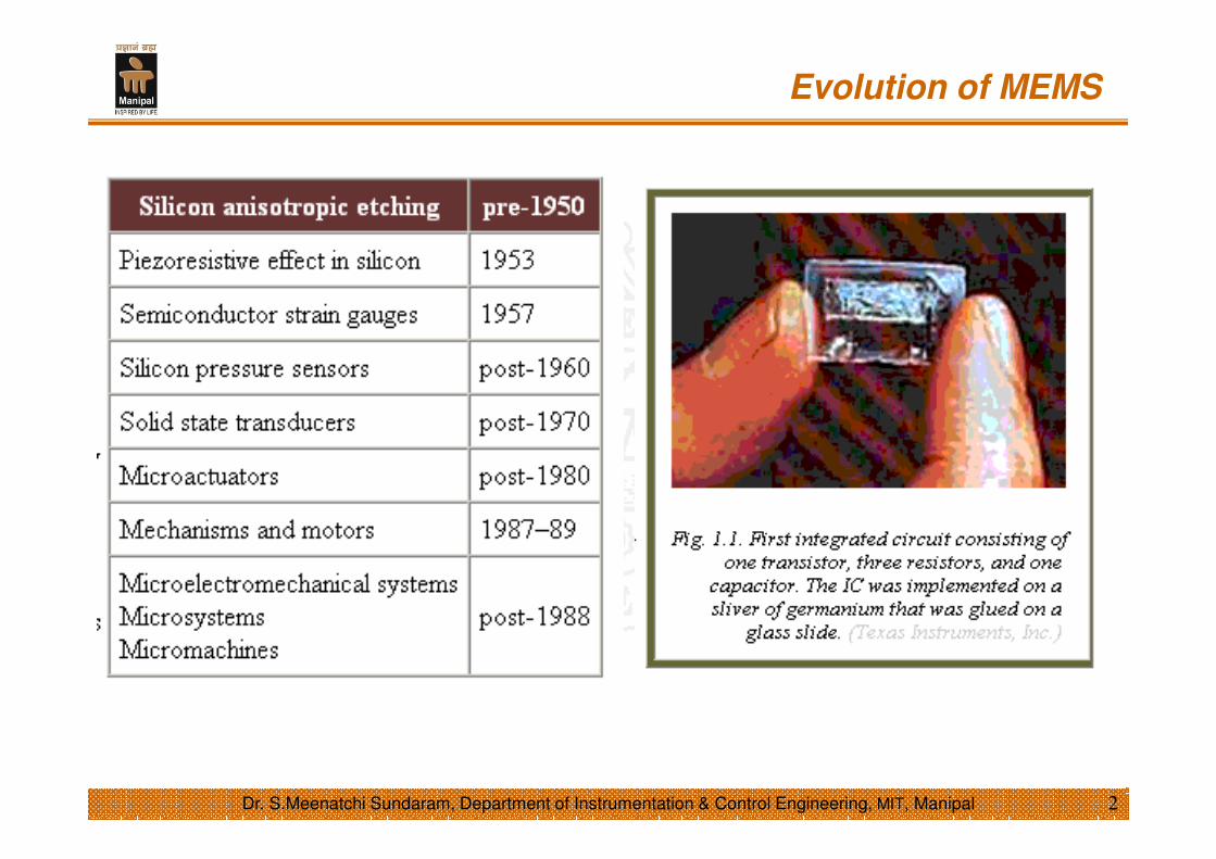
Evolution of MEMS
2Dr. S.Meenatchi Sundaram, Department of Instrumentation & Control Engineering, MIT, Manipal
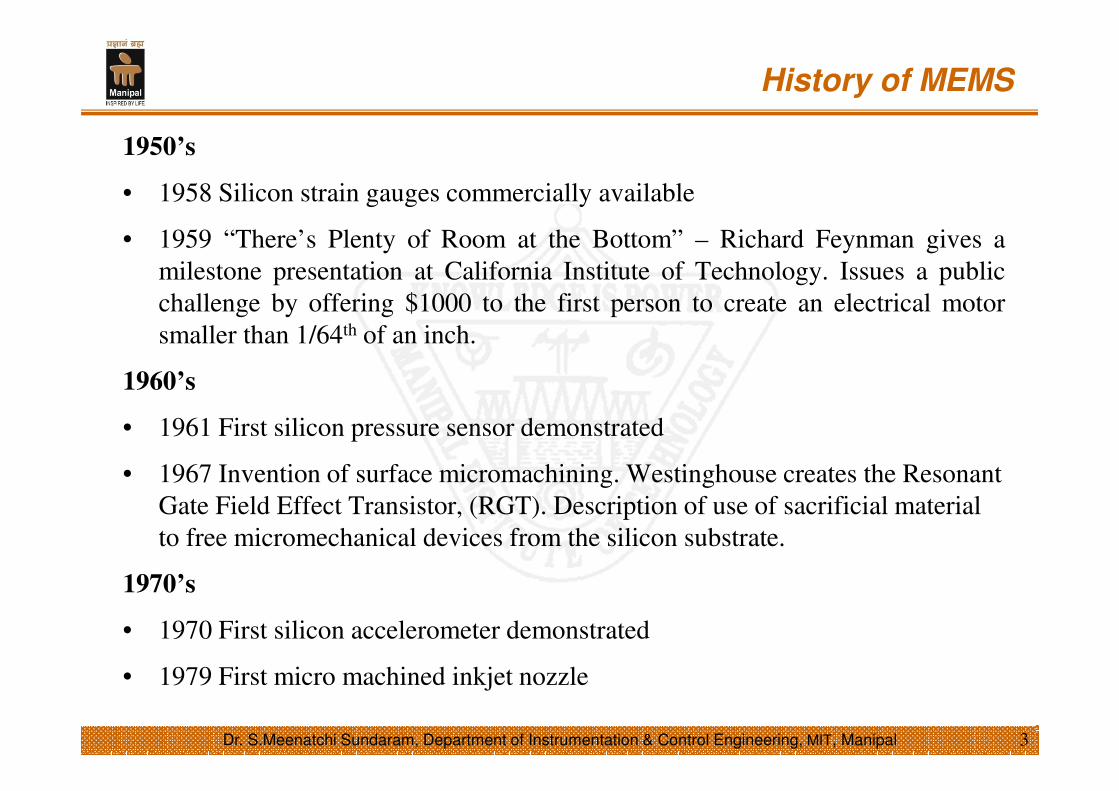
1950’s
• 1958 Silicon strain gauges commercially available
• 1959 “There’s Plenty of Room at the Bottom” – Richard Feynman gives a
milestone presentation at California Institute of Technology. Issues a public
challenge by offering $1000 to the first person to create an electrical motor
smaller than 1/64th of an inch.
1960’s
• 1961 First silicon pressure sensor demonstrated
• 1967 Invention of surface micromachining. Westinghouse creates the Resonant
Gate Field Effect Transistor, (RGT). Description of use of sacrificial material
to free micromechanical devices from the silicon substrate.
1970’s
• 1970 First silicon accelerometer demonstrated
• 1979 First micro machined inkjet nozzle
History of MEMS
3Dr. S.Meenatchi Sundaram, Department of Instrumentation & Control Engineering, MIT, Manipal
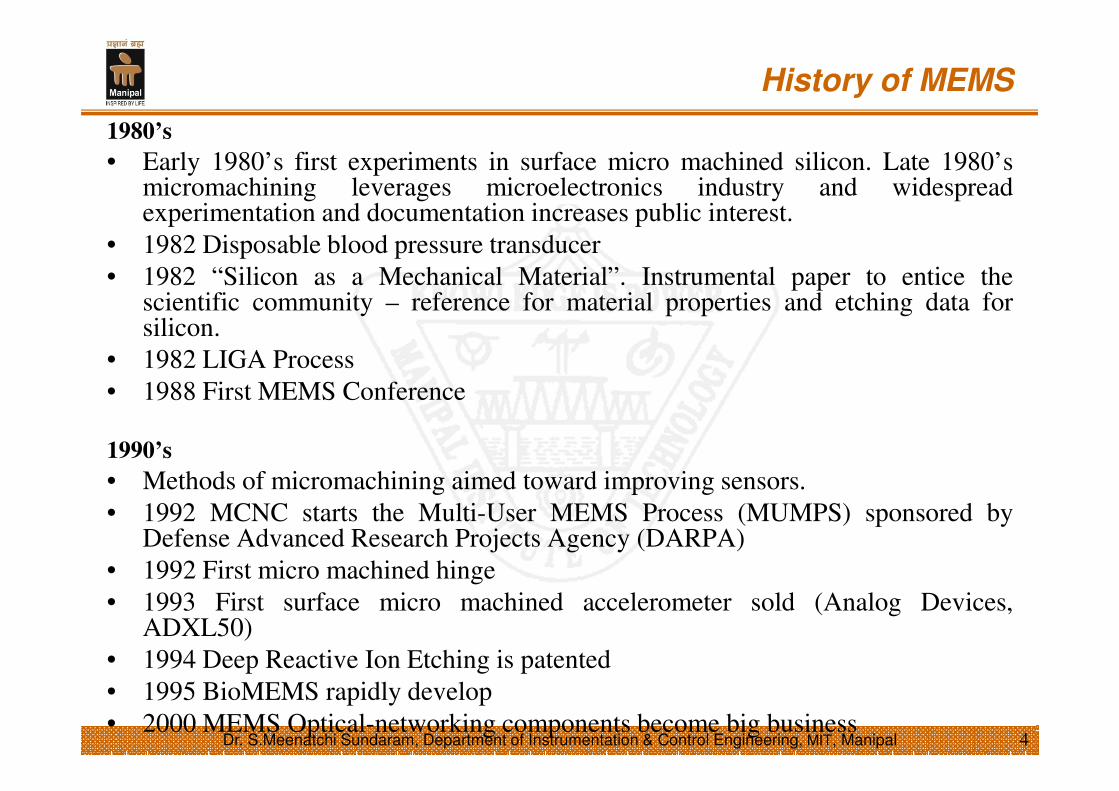
1980’s
• Early 1980’s first experiments in surface micro machined silicon. Late 1980’smicromachining leverages microelectronics industry and widespreadexperimentation and documentation increases public interest.
• 1982 Disposable blood pressure transducer
• 1982 “Silicon as a Mechanical Material”. Instrumental paper to entice thescientific community – reference for material properties and etching data forsilicon.
• 1982 LIGA Process
• 1988 First MEMS Conference
1990’s
• Methods of micromachining aimed toward improving sensors.
• 1992 MCNC starts the Multi-User MEMS Process (MUMPS) sponsored byDefense Advanced Research Projects Agency (DARPA)
• 1992 First micro machined hinge
• 1993 First surface micro machined accelerometer sold (Analog Devices,ADXL50)
• 1994 Deep Reactive Ion Etching is patented
• 1995 BioMEMS rapidly develop
• 2000 MEMS Optical-networking components become big business
History of MEMS
4Dr. S.Meenatchi Sundaram, Department of Instrumentation & Control Engineering, MIT, Manipal
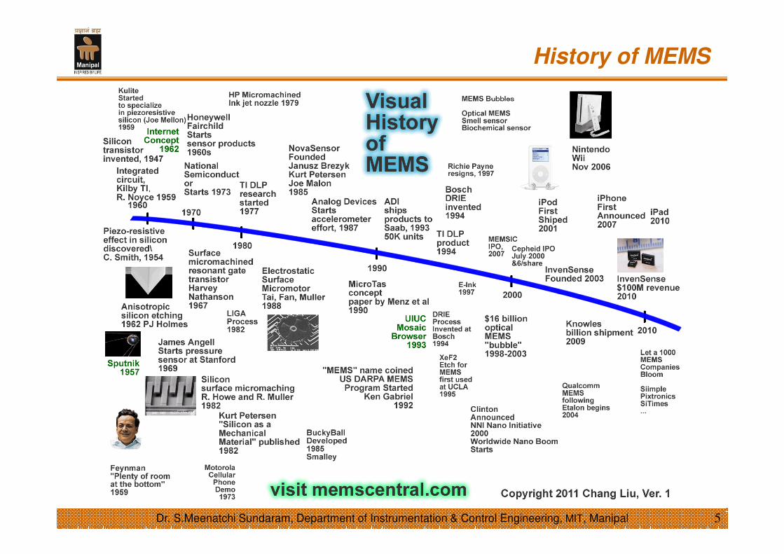
History of MEMS
5Dr. S.Meenatchi Sundaram, Department of Instrumentation & Control Engineering, MIT, Manipal
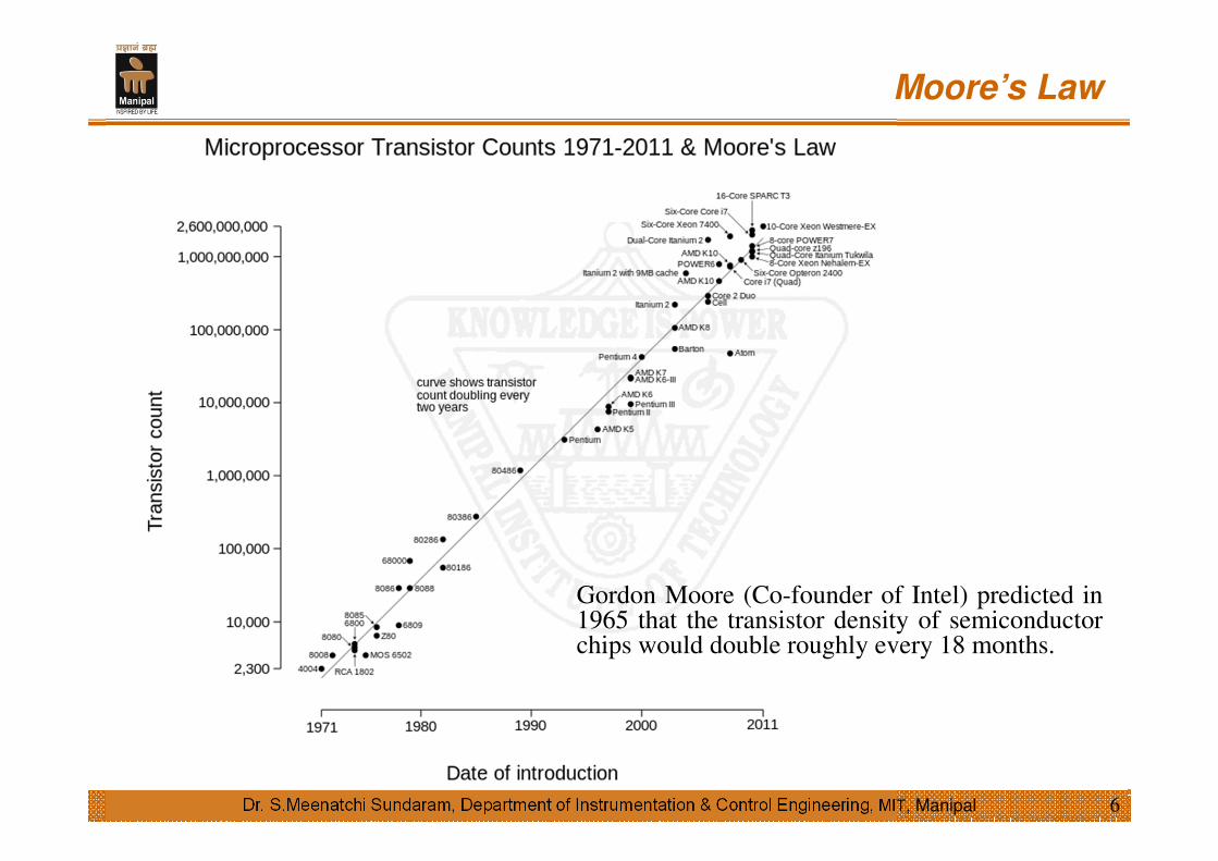
Moore’s Law
6Dr. S.Meenatchi Sundaram, Department of Instrumentation & Control Engineering, MIT, Manipal
Gordon Moore (Co-founder of Intel) predicted in1965 that the transistor density of semiconductorchips would double roughly every 18 months.
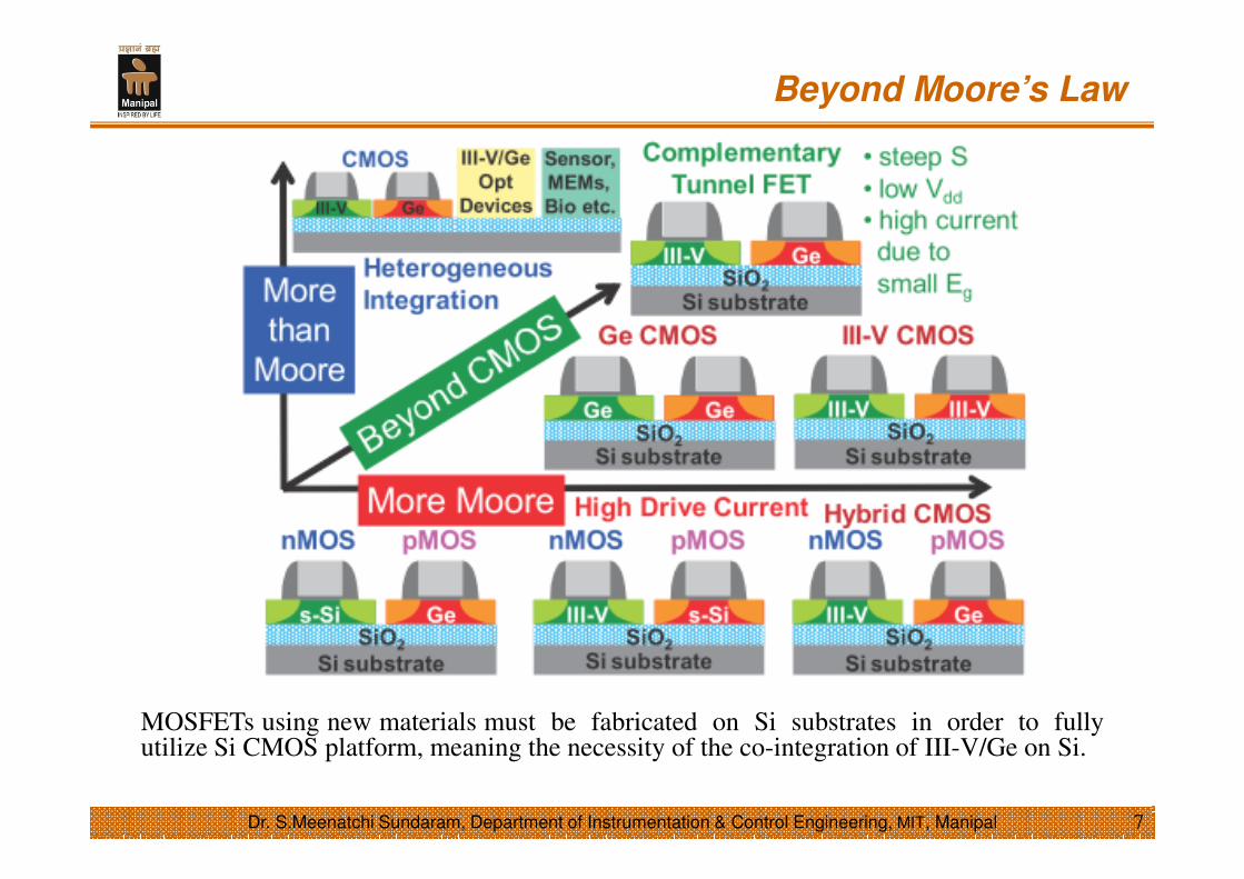
Beyond Moore’s Law
MOSFETs using new materials must be fabricated on Si substrates in order to fullyutilize Si CMOS platform, meaning the necessity of the co-integration of III-V/Ge on Si.
7Dr. S.Meenatchi Sundaram, Department of Instrumentation & Control Engineering, MIT, Manipal
The three generic and distinct characteristics of MEMS devices are:
– Miniaturization
– Microelectronics Integration
– Parallel Fabrication
Miniaturization:
• MEMS devices generally ranges from 1um to 1cm.
• May rise to operational advantages, such as,
– soft springs,
– high resonance frequency,
– Greater sensitivity
– Low thermal mass (Ex: time constant of a ink jet nozzle is typically 20us)
• Limited by scaling laws
Characteristics of MEMS
8Dr. S.Meenatchi Sundaram, Department of Instrumentation & Control Engineering, MIT, Manipal
Microelectronics Integration:
• Ability to seamlessly integrate mechanical sensors an actuators with electronics
processors an controllers at the single wafer level.
• Process paradigm referred to “Monolithic integration”
• Examples as
– Accelerometers,
– Digital Light Processors (DLP),
– Ink jet printer heads
• Dimensions and precision of placement are guaranteed by lithography.
• Quality of signals are improved by reducing noise and length of signal paths by
monolithic integration.
• In an DLP, each mirror is controlled by a CMOS logic circuit that is buried directly
underneath.
Characteristics of MEMS
9Dr. S.Meenatchi Sundaram, Department of Instrumentation & Control Engineering, MIT, Manipal
Parallel Fabrication:
• Possible to realize two or three dimensional features with small dimension and high
precision.
• High aspect ratio.
• High uniformity across wafers and batches.
Characteristics of MEMS
10Dr. S.Meenatchi Sundaram, Department of Instrumentation & Control Engineering, MIT, Manipal