Embed Size (px)
DESCRIPTION
Citation preview

On and Off-Chip Crosstalk Avoidancein VLSI Design
Chunjie Duan · Brock J. LaMeres · Sunil P. Khatri
On and Off-ChipCrosstalk Avoidancein VLSI Design
2123

AuthorsDr. Chunjie Duan Dr. Brock J. LaMeresMitsubishi Electric Research Montana State UniversityLaboratories (MERL) Dept. Electrical & Computer Engineering201 Broadway 533 Cobleigh HallCambridge, MA 02139 Bozeman, MT 59717USA [email protected] [email protected]
Dr. Sunil P. KhatriTexas A & M UniversityDept. Electrical & Computer Engineering214 Zachry Engineering CenterCollege Station, TX [email protected]
ISBN 978-1-4419-0946-6 e-ISBN 978-1-4419-0947-3DOI 10.1007/978-1-4419-0947-3Springer New York Dordrecht Heidelberg London
Library of Congress Control Number: 2009944062
© Springer Science+Business Media, LLC 2010All rights reserved. This work may not be translated or copied in whole or in part without the writtenpermission of the publisher (Springer Science+Business Media, LLC, 233 Spring Street, New York, NY10013, USA), except for brief excerpts in connection with reviews or scholarly analysis. Use in connectionwith any form of information storage and retrieval, electronic adaptation, computer software, or by similaror dissimilar methodology now known or hereafter developed is forbidden. The use in this publication oftrade names, trademarks, service marks, and similar terms, even if they are not identified as such, is notto be taken as an expression of opinion as to whether or not they are subject to proprietary rights.
Printed on acid-free paper
Springer is part of Springer Science+Business Media (www.springer.com)

Preface
One of the greatest challenges in Deep Sub-Micron (DSM) design is inter-wirecrosstalk, which becomes significant with shrinking feature sizes ofVLSI fabricationprocesses and greatly limits the speed and increases the power consumption of anIC. This monograph presents approaches to avoid crosstalk in both on-chip as wellas off-chip busses.
The research work presented in the first part of this monograph focuses on crosstalkavoidance with bus encoding, one of the techniques that effectively mitigates theimpact of on-chip capacitive crosstalk and improves the speed and power consump-tion of the bus interconnect. This technique encodes data before transmission overthe bus to avoid certain undesirable crosstalk conditions and thereby improves thebus speed and/or energy consumption. We first derive the relationship between theinter-wire capacitive crosstalk and signal speed as well as power, and show the datapattern dependence of crosstalk. A system to classify busses based on data patternsis introduced and serves as the foundation for all the on-chip crosstalk avoidanceencoding techniques. The first set of crosstalk avoidance codes (CACs) discussedare memoryless codes. These codes are generated using a fixed code-book and solelydependent on the current input data, and therefore require less complicated CODECs.We study a suite of memoryless CACs: from 3C-free to 1C-free codes, including codedesign details and performance analysis. We show that these codes are more effi-cient than conventional crosstalk avoidance techniques. We discuss several CODECdesign techniques that enable the construction of modular, fast and low overheadCODECs. The second set of codes presented are memorybased CACs. Compared tomemoryless codes, these codes are more area efficient. The corresponding CODECdesigns are more complicated, however, since the encoding/decoding processes re-quire the current input and the previous state. The memory-based codes discussedinclude a 4C-free code, which requires as little as 33% overhead with simple andfast CODEC designs. We also present two general memory-based codeword genera-tion techniques, namely the “code-pruning”-based algorithm and the ROBDD-basedalgorithm. We then further extend the crosstalk avoidance to multi-valued bus in-terconnects. The crosstalk classification system is first generalized to multi-valuedbusses and two ternary crosstalk avoidance schemes are discussed. Details about theternary driver and receiver circuit designs are also presented in the monograph.
v

vi Preface
Advances in VLSI design and fabrication technologies have led to a dramaticincrease in the on-chip performance of integrated circuits. The transistor delay inan integrated circuit is no longer the single bottleneck to system performance as ithas historically been in past decades. System performance is now also limited bythe electrical parasitics of the packaging interconnect. Noise sources such as supplybounce, signal coupling, and reflections all result in reduced performance. Thesefactors arise due to the parasitic inductance and capacitance of the packaging inter-connect. While advanced packaging can aid in reducing the parasitics, the cost andtime associated with the design of a new package is often not suited for the majorityof VLSI designs. The second part of this monograph presents techniques to modeland alleviate off-chip inductive crosstalk. This work presents techniques to modeland improve performance the performance of VLSI designs without moving towardadvanced packaging. A single, unified mathematical framework is presented that pre-dicts the performance of a given package depending on the package parasitics andbus configuration used. The performance model is shown to be accurate to within10% of analog simulator results which are much more computationally expensive.Using information about the package, a methodology is presented to select the mostcost-effective bus width for a given package. In addition, techniques are presentedto encode off-chip data so as to avoid the switching patterns that lead to increasednoise. The reduced noise level that results from encoding the off-chip data translatesinto increased bus performance even after accounting for the encoder overhead. Per-formance improvements of up to 225% are reported using the encoding techniques.Finally, a compensation technique is presented that matches the impedance of thepackage interconnect to the impedance of the PCB, resulting in reduced reflectednoise. The compensation technique is shown to reduce reflected noise as much as400% for broadband frequencies up to 3 GHz. The techniques presented in this workare described in general terms so as not to limit the approach to any particular tech-nology. At the same time, the techniques are validated using existing technologiesto prove their effectiveness.
The authors would like to thank Ericsson Wireless Communications in Boulder,Colorado, Mitsubishi Electric Research Laboratories in Cambridge, Massachusettsand Agilent Technologies in Colorado Springs for funding some of the researchworks presented in this monograph. Agilent Technologies also provided instrumen-tation, EDA tools, and hardware used in the development and analysis of the off-chipcrosstalk avoidance techniques in this monograph. The authors would also like tothank Xilinx Corporation for providing the FPGA devices and design methodolo-gies necessary for prototyping the techniques in this monograph and evaluating theirfeasibility.
August 2009 Chunjie DuanBrock J. LaMeres
Sunil P. Khatri

Acknowledgements
Dr. Duan is grateful to his parents, Derong and Xingling, and his beautiful wife, Ruifor their unconditional support over the years. Without their support, research wouldhave been a lot more painful experience than it already is.
Dr. LaMeres would like to thank his family for all of the support they have givenover the years. Endless thanks for offered to his wonderful wife, JoAnn, and to histwo precious daughters, Alexis and Kylie, who have given up too many nights andweekends of family time for the pursuit of research in this area. Their sacrifice willalways be remembered.
Dr. Khatri would like to thank his family for their support and encouragementover the years, without which this book and many other research endeavors wouldsimply not have been possible.
vii
Contents
Part I On-Chip Crosstalk and Avoidance . . . . . . . . . . . . . . . . . . . . . . . . . . . . 1
1 Introduction of On-Chip Crosstalk Avoidance . . . . . . . . . . . . . . . . . . . . . 31.1 Challenges in Deep Submicron Processes . . . . . . . . . . . . . . . . . . . . . . 31.2 Overview of On-Chip Crosstalk Avoidance . . . . . . . . . . . . . . . . . . . . 41.3 Bus Encoding for Crosstalk Avoidance . . . . . . . . . . . . . . . . . . . . . . . . 91.4 Part I Organization . . . . . . . . . . . . . . . . . . . . . . . . . . . . . . . . . . . . . . . . . 10
2 Preliminaries to On-Chip Crosstalk . . . . . . . . . . . . . . . . . . . . . . . . . . . . . . 132.1 Modeling of On-Chip Interconnects . . . . . . . . . . . . . . . . . . . . . . . . . . 132.2 Crosstalk Based Bus Classification . . . . . . . . . . . . . . . . . . . . . . . . . . . 222.3 Bus Encoding for Crosstalk Avoidance . . . . . . . . . . . . . . . . . . . . . . . . 242.4 Notation and Terminology . . . . . . . . . . . . . . . . . . . . . . . . . . . . . . . . . . 25
3 Memoryless Crosstalk Avoidance Codes . . . . . . . . . . . . . . . . . . . . . . . . . . 273.1 3C-Free CACs . . . . . . . . . . . . . . . . . . . . . . . . . . . . . . . . . . . . . . . . . . . . 27
3.1.1 Forbidden Pattern Free CAC . . . . . . . . . . . . . . . . . . . . . . . . . . 283.1.2 Forbidden Transition Free CAC . . . . . . . . . . . . . . . . . . . . . . . 323.1.3 Circuit Implementation and Simulation Results . . . . . . . . . . 35
3.2 2C-Free CACs . . . . . . . . . . . . . . . . . . . . . . . . . . . . . . . . . . . . . . . . . . . . 373.2.1 Code Construction . . . . . . . . . . . . . . . . . . . . . . . . . . . . . . . . . . 383.2.2 Code Cardinality and Area Overhead . . . . . . . . . . . . . . . . . . . 403.2.3 2C Experiments . . . . . . . . . . . . . . . . . . . . . . . . . . . . . . . . . . . . . 42
3.3 1C-Free Busses . . . . . . . . . . . . . . . . . . . . . . . . . . . . . . . . . . . . . . . . . . . 423.3.1 Bus Configurations . . . . . . . . . . . . . . . . . . . . . . . . . . . . . . . . . . 433.3.2 Experimental Results . . . . . . . . . . . . . . . . . . . . . . . . . . . . . . . . 43
3.4 Summary . . . . . . . . . . . . . . . . . . . . . . . . . . . . . . . . . . . . . . . . . . . . . . . . . 44
4 CODEC Designs for Memoryless Crosstalk Avoidance Codes . . . . . . . 474.1 Bus Partitioning Based CODEC Design Techniques . . . . . . . . . . . . . 474.2 Group Complement . . . . . . . . . . . . . . . . . . . . . . . . . . . . . . . . . . . . . . . . 48
4.2.1 Proof of Correctness . . . . . . . . . . . . . . . . . . . . . . . . . . . . . . . . . 504.3 Bit Overlapping . . . . . . . . . . . . . . . . . . . . . . . . . . . . . . . . . . . . . . . . . . . 51
ix
x Contents
4.4 FPF-CAC CODEC Design . . . . . . . . . . . . . . . . . . . . . . . . . . . . . . . . . . 514.4.1 Fibonacci-Based Binary Numeral System . . . . . . . . . . . . . . . 524.4.2 Near-Optimal CODEC . . . . . . . . . . . . . . . . . . . . . . . . . . . . . . . 534.4.3 Optimal CODEC . . . . . . . . . . . . . . . . . . . . . . . . . . . . . . . . . . . . 574.4.4 Implementation and Experimental Results . . . . . . . . . . . . . . . 59
4.5 FTF-CAC CODEC Design . . . . . . . . . . . . . . . . . . . . . . . . . . . . . . . . . . 654.5.1 Mapping Scheme . . . . . . . . . . . . . . . . . . . . . . . . . . . . . . . . . . . 654.5.2 Coding Algorithm . . . . . . . . . . . . . . . . . . . . . . . . . . . . . . . . . . . 664.5.3 Implementation and Experimental Results . . . . . . . . . . . . . . . 67
4.6 Summary . . . . . . . . . . . . . . . . . . . . . . . . . . . . . . . . . . . . . . . . . . . . . . . . . 70
5 Memory-based Crosstalk Avoidance Codes . . . . . . . . . . . . . . . . . . . . . . . . 735.1 A 4C-Free CAC . . . . . . . . . . . . . . . . . . . . . . . . . . . . . . . . . . . . . . . . . . . 73
5.1.1 A 4C-free Encoding Technique . . . . . . . . . . . . . . . . . . . . . . . . 735.1.2 An Example . . . . . . . . . . . . . . . . . . . . . . . . . . . . . . . . . . . . . . . . 74
5.2 Codeword Generation by Pruning . . . . . . . . . . . . . . . . . . . . . . . . . . . . 755.3 Codeword Generation Using ROBDD . . . . . . . . . . . . . . . . . . . . . . . . . 80
5.3.1 Efficient Construction of Gkc−freem . . . . . . . . . . . . . . . . . . . . . . 80
5.3.2 An Example . . . . . . . . . . . . . . . . . . . . . . . . . . . . . . . . . . . . . . . . 825.3.3 Finding the Effective kC Free Bus Width from Gkc−free
m . . . . 835.3.4 Experimental Results . . . . . . . . . . . . . . . . . . . . . . . . . . . . . . . . 84
5.4 Summary . . . . . . . . . . . . . . . . . . . . . . . . . . . . . . . . . . . . . . . . . . . . . . . . . 85
6 Multi-Valued Logic Crosstalk Avoidance Codes . . . . . . . . . . . . . . . . . . . . 876.1 Bus Classification in Multi-Valued Busses . . . . . . . . . . . . . . . . . . . . . 886.2 Low Power and Crosstalk Avoiding Coding on a Ternary Bus . . . . . 90
6.2.1 Direct Binary-Ternary Mapping . . . . . . . . . . . . . . . . . . . . . . . 906.2.2 4X Ternary Code . . . . . . . . . . . . . . . . . . . . . . . . . . . . . . . . . . . . 916.2.3 3X Ternary Code . . . . . . . . . . . . . . . . . . . . . . . . . . . . . . . . . . . . 93
6.3 Circuit Implementations . . . . . . . . . . . . . . . . . . . . . . . . . . . . . . . . . . . . 946.4 Experimental Results . . . . . . . . . . . . . . . . . . . . . . . . . . . . . . . . . . . . . . . 956.5 Summary . . . . . . . . . . . . . . . . . . . . . . . . . . . . . . . . . . . . . . . . . . . . . . . . 98
7 Summary of On-Chip Crosstalk Avoidance . . . . . . . . . . . . . . . . . . . . . . . . 101
Part II Off-Chip Crosstalk and Avoidance . . . . . . . . . . . . . . . . . . . . . . . . . . . 105
8 Introduction to Off-Chip Crosstalk . . . . . . . . . . . . . . . . . . . . . . . . . . . . . . 1078.1 The Role of IC Packaging . . . . . . . . . . . . . . . . . . . . . . . . . . . . . . . . . . . 1078.2 Noise Sources in Packaging . . . . . . . . . . . . . . . . . . . . . . . . . . . . . . . . . 109
8.2.1 Inductive Supply Bounce . . . . . . . . . . . . . . . . . . . . . . . . . . . . . 1098.2.2 Inductive Signal Coupling . . . . . . . . . . . . . . . . . . . . . . . . . . . . 1118.2.3 Capacitive Bandwidth Limiting . . . . . . . . . . . . . . . . . . . . . . . . 1138.2.4 Capacitive Signal Coupling . . . . . . . . . . . . . . . . . . . . . . . . . . . 1148.2.5 Impedance Discontinuities . . . . . . . . . . . . . . . . . . . . . . . . . . . . 115

Contents xi
8.3 Performance Modeling and Proposed Techniques . . . . . . . . . . . . . . . 1178.3.1 Performance Modeling . . . . . . . . . . . . . . . . . . . . . . . . . . . . . . . 1178.3.2 Optimal Bus Sizing . . . . . . . . . . . . . . . . . . . . . . . . . . . . . . . . . . 1178.3.3 Bus Encoding . . . . . . . . . . . . . . . . . . . . . . . . . . . . . . . . . . . . . . 1188.3.4 Impedance Compensation . . . . . . . . . . . . . . . . . . . . . . . . . . . . 119
8.4 Advantages Over Prior Techniques . . . . . . . . . . . . . . . . . . . . . . . . . . . 1208.4.1 Performance Modeling . . . . . . . . . . . . . . . . . . . . . . . . . . . . . . . 1208.4.2 Optimal Bus Sizing . . . . . . . . . . . . . . . . . . . . . . . . . . . . . . . . . . 1218.4.3 Bus Encoding . . . . . . . . . . . . . . . . . . . . . . . . . . . . . . . . . . . . . . 1228.4.4 Impedance Compensation . . . . . . . . . . . . . . . . . . . . . . . . . . . . 123
8.5 Broader Impact of This Monograph . . . . . . . . . . . . . . . . . . . . . . . . . . . 1238.6 Organization of Part II of this Monograph . . . . . . . . . . . . . . . . . . . . . 124
9 Package Construction and Electrical Modeling . . . . . . . . . . . . . . . . . . . . 1259.1 Level 1 Interconnect . . . . . . . . . . . . . . . . . . . . . . . . . . . . . . . . . . . . . . . 125
9.1.1 Wire Bonding . . . . . . . . . . . . . . . . . . . . . . . . . . . . . . . . . . . . . . 1259.1.2 Flip-Chip Bumping . . . . . . . . . . . . . . . . . . . . . . . . . . . . . . . . . . 127
9.2 Level 2 Interconnect . . . . . . . . . . . . . . . . . . . . . . . . . . . . . . . . . . . . . . . 1299.2.1 Lead Frame . . . . . . . . . . . . . . . . . . . . . . . . . . . . . . . . . . . . . . . . 1299.2.2 Array Pattern . . . . . . . . . . . . . . . . . . . . . . . . . . . . . . . . . . . . . . . 130
9.3 Modern Packages . . . . . . . . . . . . . . . . . . . . . . . . . . . . . . . . . . . . . . . . . . 1319.3.1 Quad Flat Pack with Wire Bonding . . . . . . . . . . . . . . . . . . . . . 1329.3.2 Ball Grid Array with Wire Bonding . . . . . . . . . . . . . . . . . . . . 1339.3.3 Ball Grid Array with Flip-Chip Bumping . . . . . . . . . . . . . . . . 134
9.4 Electrical Modeling . . . . . . . . . . . . . . . . . . . . . . . . . . . . . . . . . . . . . . . . 1359.4.1 Quad Flat Pack with Wire Bonding . . . . . . . . . . . . . . . . . . . . . 1359.4.2 Ball Grid Array with Wire Bonding . . . . . . . . . . . . . . . . . . . . 1359.4.3 Ball Grid Array with Flip-Chip Bumping . . . . . . . . . . . . . . . . 136
10 Preliminaries and Terminology . . . . . . . . . . . . . . . . . . . . . . . . . . . . . . . . . . 13710.1 Bus Construction . . . . . . . . . . . . . . . . . . . . . . . . . . . . . . . . . . . . . . . . . . 13710.2 Logic Values and Transitions . . . . . . . . . . . . . . . . . . . . . . . . . . . . . . . . 13910.3 Signal Coupling . . . . . . . . . . . . . . . . . . . . . . . . . . . . . . . . . . . . . . . . . . . 140
10.3.1 Mutual Inductive Signal Coupling . . . . . . . . . . . . . . . . . . . . . 14010.3.2 Mutual Capacitive Signal Coupling . . . . . . . . . . . . . . . . . . . . 141
10.4 Return Current . . . . . . . . . . . . . . . . . . . . . . . . . . . . . . . . . . . . . . . . . . . . 14110.5 Noise Limits . . . . . . . . . . . . . . . . . . . . . . . . . . . . . . . . . . . . . . . . . . . . . . 142
11 Analytical Model for Off-Chip Bus Performance . . . . . . . . . . . . . . . . . . . 14511.1 Package Performance Metrics . . . . . . . . . . . . . . . . . . . . . . . . . . . . . . . 14511.2 Converting Performance to Risetime . . . . . . . . . . . . . . . . . . . . . . . . . . 14611.3 Converting Bus Performance to di
dt and dvdt . . . . . . . . . . . . . . . . . . . . . . 147
11.4 Translating Noise Limits to Performance . . . . . . . . . . . . . . . . . . . . . . 14811.4.1 Inductive Supply Bounce . . . . . . . . . . . . . . . . . . . . . . . . . . . . . 14811.4.2 Capacitive Bandwidth Limiting . . . . . . . . . . . . . . . . . . . . . . . . 150

xii Contents
11.4.3 Signal Coupling . . . . . . . . . . . . . . . . . . . . . . . . . . . . . . . . . . . . . 15111.4.4 Impedance Discontinuities . . . . . . . . . . . . . . . . . . . . . . . . . . . . 152
11.5 Experimental Results . . . . . . . . . . . . . . . . . . . . . . . . . . . . . . . . . . . . . . . 15211.5.1 Test Circuit . . . . . . . . . . . . . . . . . . . . . . . . . . . . . . . . . . . . . . . . 15311.5.2 Quad Flat Pack with Wire Bonding Results . . . . . . . . . . . . . . 15411.5.3 Ball Grid Array with Wire Bonding Results . . . . . . . . . . . . . . 15611.5.4 Ball Grid Array with Flip-Chip Bumping Results . . . . . . . . . 15711.5.5 Discussion . . . . . . . . . . . . . . . . . . . . . . . . . . . . . . . . . . . . . . . . . 159
12 Optimal Bus Sizing . . . . . . . . . . . . . . . . . . . . . . . . . . . . . . . . . . . . . . . . . . . . . 16112.1 Package Cost . . . . . . . . . . . . . . . . . . . . . . . . . . . . . . . . . . . . . . . . . . . . . 16112.2 Bandwidth Per Cost . . . . . . . . . . . . . . . . . . . . . . . . . . . . . . . . . . . . . . . . 163
12.2.1 Results for Quad Flat Pack with Wire Bonding . . . . . . . . . . . 16312.2.2 Results for Ball Grid Array with Wire Bonding . . . . . . . . . . . 16412.2.3 Results for Ball Grid Array with Flip-Chip Bumping . . . . . . 164
12.3 Bus Sizing Example . . . . . . . . . . . . . . . . . . . . . . . . . . . . . . . . . . . . . . . . 166
13 Bus Expansion Encoder . . . . . . . . . . . . . . . . . . . . . . . . . . . . . . . . . . . . . . . . . 16713.1 Constraint Equations . . . . . . . . . . . . . . . . . . . . . . . . . . . . . . . . . . . . . . . 167
13.1.1 Supply Bounce Constraints . . . . . . . . . . . . . . . . . . . . . . . . . . . 16813.1.2 Signal Coupling Constraints . . . . . . . . . . . . . . . . . . . . . . . . . . 16813.1.3 Capacitive Bandwidth Limiting Constraints . . . . . . . . . . . . . 17013.1.4 Impedance Discontinuity Constraints . . . . . . . . . . . . . . . . . . . 17113.1.5 Number of Constraint Equations . . . . . . . . . . . . . . . . . . . . . . . 17213.1.6 Number of Constraint Evaluations . . . . . . . . . . . . . . . . . . . . . 172
13.2 Encoder Construction . . . . . . . . . . . . . . . . . . . . . . . . . . . . . . . . . . . . . . 17313.2.1 Encoder Algorithm . . . . . . . . . . . . . . . . . . . . . . . . . . . . . . . . . . 17313.2.2 Encoder Overhead . . . . . . . . . . . . . . . . . . . . . . . . . . . . . . . . . . . 175
13.3 Decoder Construction . . . . . . . . . . . . . . . . . . . . . . . . . . . . . . . . . . . . . . 17513.4 Experimental Results . . . . . . . . . . . . . . . . . . . . . . . . . . . . . . . . . . . . . . . 175
13.4.1 3-Bit Fixed didt Example . . . . . . . . . . . . . . . . . . . . . . . . . . . . . . 176
13.4.2 3-Bit Varying didt Example . . . . . . . . . . . . . . . . . . . . . . . . . . . . . 180
13.4.3 Functional Implementation . . . . . . . . . . . . . . . . . . . . . . . . . . . 18213.4.4 Physical Implementation . . . . . . . . . . . . . . . . . . . . . . . . . . . . . 18313.4.5 Measurement Results . . . . . . . . . . . . . . . . . . . . . . . . . . . . . . . . 185
14 Bus Stuttering Encoder . . . . . . . . . . . . . . . . . . . . . . . . . . . . . . . . . . . . . . . . . 18914.1 Encoder Construction . . . . . . . . . . . . . . . . . . . . . . . . . . . . . . . . . . . . . . 189
14.1.1 Encoder Algorithm . . . . . . . . . . . . . . . . . . . . . . . . . . . . . . . . . . 19014.1.2 Encoder Overhead . . . . . . . . . . . . . . . . . . . . . . . . . . . . . . . . . . . 191
14.2 Decoder Construction . . . . . . . . . . . . . . . . . . . . . . . . . . . . . . . . . . . . . . 19214.3 Experimental Results . . . . . . . . . . . . . . . . . . . . . . . . . . . . . . . . . . . . . . . 192
14.3.1 Functional Implementation . . . . . . . . . . . . . . . . . . . . . . . . . . . 19414.3.2 Physical Implementation . . . . . . . . . . . . . . . . . . . . . . . . . . . . . 196
Contents xiii
14.3.3 Measurement Results . . . . . . . . . . . . . . . . . . . . . . . . . . . . . . . . 19714.3.4 Discussion . . . . . . . . . . . . . . . . . . . . . . . . . . . . . . . . . . . . . . . . . 198
15 Impedance Compensation . . . . . . . . . . . . . . . . . . . . . . . . . . . . . . . . . . . . . . . 20115.1 Static Compensator . . . . . . . . . . . . . . . . . . . . . . . . . . . . . . . . . . . . . . . . 202
15.1.1 Methodology . . . . . . . . . . . . . . . . . . . . . . . . . . . . . . . . . . . . . . . 20215.1.2 Compensator Proximity . . . . . . . . . . . . . . . . . . . . . . . . . . . . . . 20315.1.3 On-Chip Capacitors . . . . . . . . . . . . . . . . . . . . . . . . . . . . . . . . . 20315.1.4 On-Package Capacitors . . . . . . . . . . . . . . . . . . . . . . . . . . . . . . 20515.1.5 Static Compensator Design . . . . . . . . . . . . . . . . . . . . . . . . . . . 20515.1.6 Experimental Results . . . . . . . . . . . . . . . . . . . . . . . . . . . . . . . . 207
15.2 Dynamic Compensator . . . . . . . . . . . . . . . . . . . . . . . . . . . . . . . . . . . . . 21015.2.1 Methodology . . . . . . . . . . . . . . . . . . . . . . . . . . . . . . . . . . . . . . . 21015.2.2 Dynamic Compensator Design . . . . . . . . . . . . . . . . . . . . . . . . 21015.2.3 Experimental Results . . . . . . . . . . . . . . . . . . . . . . . . . . . . . . . . 21315.2.4 Dynamic Compensator Calibration . . . . . . . . . . . . . . . . . . . . . 216
16 Future Trends and Applications . . . . . . . . . . . . . . . . . . . . . . . . . . . . . . . . . . 21916.1 The Move from ASICs to FPGAs. . . . . . . . . . . . . . . . . . . . . . . . . . . . . 21916.2 IP Cores . . . . . . . . . . . . . . . . . . . . . . . . . . . . . . . . . . . . . . . . . . . . . . . . . 22216.3 Power Minimization . . . . . . . . . . . . . . . . . . . . . . . . . . . . . . . . . . . . . . . 22316.4 Connectors and Backplanes . . . . . . . . . . . . . . . . . . . . . . . . . . . . . . . . . 22416.5 Internet Fabric . . . . . . . . . . . . . . . . . . . . . . . . . . . . . . . . . . . . . . . . . . . . 225
17 Summary of Off-Chip Crosstalk Avoidance . . . . . . . . . . . . . . . . . . . . . . . 227
References . . . . . . . . . . . . . . . . . . . . . . . . . . . . . . . . . . . . . . . . . . . . . . . . . . . . . . . . 231
Index . . . . . . . . . . . . . . . . . . . . . . . . . . . . . . . . . . . . . . . . . . . . . . . . . . . . . . . . . . . . 239

Abbreviations
ASIC Application Specific Integrated CircuitBGA Ball Grid ArrayCAC Crosstalk Avoidance CodeCMP Chip-level MultiprocessingCMOS Complementary Metal-Oxide-SemiconductorCODEC Encoder and DecoderDSM Deep SubmicronFC Flip ChipFPF Forbidden Pattern FreeFPGA Field Programmable Gate ArrayFNS Fibonacci-based Numeral SystemFTF Forbidden Transition FreeLSB Least Significant BitMSB Most Significant BitNoC Network on ChipPAM Pulse Amplitude ModulationPDP Power-Delay ProductPCB Printed Circuit BoardPWB PrintedWiring BoardPLA Programmable Logic ArrayQFP Quad Flat PackROBDD Reduced Ordered Binary Decision DiagramSoC System on ChipSoI Silicon on InsulatorVLSI Very Large Scale Integrated CircuitWB Wire Bond
xv

List of Figures
1.1 On-chip bus model with crosstalk . . . . . . . . . . . . . . . . . . . . . . . . . . . . . . . 41.2 An example of arrangement of conductors in the PLA
core [61] . . . . . . . . . . . . . . . . . . . . . . . . . . . . . . . . . . . . . . . . . . . . . . . . . . . 51.3 Signal delay improvement using intentional skewing [44].
a shows the signal waveform of a synchronous bus andb shows the signal waveform of bus with intentional skewingimplemented . . . . . . . . . . . . . . . . . . . . . . . . . . . . . . . . . . . . . . . . . . . . . . . . 6
1.4 Illustration of repeater interleaving . . . . . . . . . . . . . . . . . . . . . . . . . . . . . . 71.5 Twisted differential pairs with offset twists [45] . . . . . . . . . . . . . . . . . . . 8
2.1 3-D structure of an on-chip conductor . . . . . . . . . . . . . . . . . . . . . . . . . . . 142.2 A simplified 3-D structure of an on-chip bus . . . . . . . . . . . . . . . . . . . . . 152.3 Equivalent circuit for the data bus a Lumped RC model
b Distributed RC model using 2π -sections . . . . . . . . . . . . . . . . . . . . . . . 172.4 Equivalent circuits for the drivers a Vj high b Vj low . . . . . . . . . . . . . . . 182.5 Sample signal waveforms under different crosstalk conditions
(60× driver, 2 cm trace length, 0.1 μ process) . . . . . . . . . . . . . . . . . . . . . 242.6 Bus encoding for crosstalk avoidance . . . . . . . . . . . . . . . . . . . . . . . . . . . 24
3.1 Percentage overhead . . . . . . . . . . . . . . . . . . . . . . . . . . . . . . . . . . . . . . . . . . 323.2 Bus signal waveforms. Bus is 20 mm long and the driver size is 60×
the minimum size, implemented in a 0.1 μm process a Signalwaveform on the bus without coding b Signal waveform on the buswith coding . . . . . . . . . . . . . . . . . . . . . . . . . . . . . . . . . . . . . . . . . . . . . . . . . 36
3.3 Signal waveforms at the receiver output. Bus is 20 mm long and thedriver size is 60× the minimum size, implemented in 0.1 μm processa Receiver output waveform on the bus without coding b Receiveroutput waveform on the bus with coding . . . . . . . . . . . . . . . . . . . . . . . . . 37
3.4 Effective versus actual bus width for 2C-free CACs. . . . . . . . . . . . . . . . 42
xvii

xviii List of Figures
3.5 1C free bus configurations a 3-wire group, fixed spacing within group,variable spacing between groups b 3-wire group with shielding betweengroups, fixed spacing within group, variable spacing between groupsc no shielding wires, variable wire sizes and spacing d 5-wire group,fixed spacing within group, variable spacing between groups . . . . . . . . 43
3.6 Delay versus area tradeoff for 1C schemes . . . . . . . . . . . . . . . . . . . . . . . 44
4.1 Gate count of flat look-up table based FTF encoder designs [89] . . . . . 484.2 A 16-bit group complement FPF CODEC structure . . . . . . . . . . . . . . . . 494.3 FPF bit-overlapping encoder . . . . . . . . . . . . . . . . . . . . . . . . . . . . . . . . . . . 514.4 FPF CODEC structure (based on Algorithm 4.1) . . . . . . . . . . . . . . . . . . 564.5 Internal logic of the kth block in the FPF encoder . . . . . . . . . . . . . . . . . 604.6 An FPF CODEC structure with optimized MSB stage . . . . . . . . . . . . . . 614.7 Resource utilization and delay of the FPF encoders for different
input bus sizes in FPGA implementation . . . . . . . . . . . . . . . . . . . . . . . . . 614.8 Gate count and delay of FPF encoders for different input bus sizes in
TSMC 90 nm ASIC implementation . . . . . . . . . . . . . . . . . . . . . . . . . . . . . 624.9 Gate count comparison for different FPF encoder implementations
in a TSMC 90 nm ASIC process: a random mapping based flatimplementation, an FNS-based flat implementation and an FNS-basedmulti-stage implementation . . . . . . . . . . . . . . . . . . . . . . . . . . . . . . . . . . . . 63
4.10 FPF CODEC block diagram with bus partition for delay/areaimprovement . . . . . . . . . . . . . . . . . . . . . . . . . . . . . . . . . . . . . . . . . . . . . . . . 64
4.11 Range of the vectors with MSBs of “00”, “01”, “10” and “11” . . . . . . . 654.12 FTF encoder and decoder block diagram . . . . . . . . . . . . . . . . . . . . . . . . . 684.13 FTF and FPF encoder gate count comparison . . . . . . . . . . . . . . . . . . . . . 694.14 FTF CODECs combined with bus partitioning . . . . . . . . . . . . . . . . . . . . 70
5.1 Graphs for 3-bit busses under different crosstalk constraintsa G3 graph b G4C−free
3 graph c G3C−free3 graph d G2C−free
3 graph
e G1C−free3 graph . . . . . . . . . . . . . . . . . . . . . . . . . . . . . . . . . . . . . . . . . . . . . 76
5.2 Pruning iteration of a 3-bit 1C transition graph a In the initial graph,min(dG1C
3(v)) = 3 and |G| = 8. Two vertices of degree 3 are 010 and
101. b In first iteration, vertices with fewest edges are removed (dash-lined circles). Edges incident to them are deleted (shown as dashlines). In the resulting subgraph G′, minv∈V ′ (dG′ (v)) = 4 and|G′| = 6 c In the second iteration. 4 vertices with fewest edges areremoved. minv∈V ′ (dG′ (v)) = 2 and |G′| = 2 d After the final iteration,the resulting subgraph is an empty graph (all vertices are removed).minv∈V ′ (dG′ (v)) = 0, |G′| = 0 . . . . . . . . . . . . . . . . . . . . . . . . . . . . . . . . . . 78
5.3 Area overhead comparision between FTF codes and memory-basedcodes generated with class pruning . . . . . . . . . . . . . . . . . . . . . . . . . . . . . . 79
5.4 Bus size overheads for Memory-based CODECs . . . . . . . . . . . . . . . . . . 85

List of Figures xix
6.1 Illustration of a 4-valued logic waveforms . . . . . . . . . . . . . . . . . . . . . . . . 886.2 4X encoder and driver circuit . . . . . . . . . . . . . . . . . . . . . . . . . . . . . . . . . . 926.3 Current-mode and Voltage-mode busses a Current-mode bus driver
and receiver b Voltage- mode bus driver and receiver . . . . . . . . . . . . . . . 946.4 On-chip Vdd /2 generation . . . . . . . . . . . . . . . . . . . . . . . . . . . . . . . . . . . . . 956.5 Crosstalk distributions . . . . . . . . . . . . . . . . . . . . . . . . . . . . . . . . . . . . . . . . 976.6 Ternary bus eye-diagrams a Uncoded ternary bus
b 4X ternary bus . . . . . . . . . . . . . . . . . . . . . . . . . . . . . . . . . . . . . . . . . . . . . 98
8.1 Ideal CMOS inverter circuit . . . . . . . . . . . . . . . . . . . . . . . . . . . . . . . . . . . 1108.2 CMOS inverter circuit with supply inductance . . . . . . . . . . . . . . . . . . . . 1118.3 Circuit description of inductive signal coupling . . . . . . . . . . . . . . . . . . . 1128.4 Circuit description of capacitive bandwidth limiting . . . . . . . . . . . . . . . 1148.5 Circuit description of capacitive signal coupling . . . . . . . . . . . . . . . . . . 1158.6 Circuit description of a distributed transmission line . . . . . . . . . . . . . . . 1168.7 Performance improvement using proposed techniques . . . . . . . . . . . . . . 120
9.1 SEM photograph of ball bond connection . . . . . . . . . . . . . . . . . . . . . . . . 1269.2 SEM photograph of wedge bond connection . . . . . . . . . . . . . . . . . . . . . . 1269.3 SEM photograph of a wire bonded system . . . . . . . . . . . . . . . . . . . . . . . 1279.4 SEM photograph of flip-chip bump array . . . . . . . . . . . . . . . . . . . . . . . . 1289.5 Lead frame connection to IC substrate . . . . . . . . . . . . . . . . . . . . . . . . . . . 1309.6 SEM photograph of the bottom of a 1 mm pitch BGA package . . . . . . 1319.7 Photograph of a 1 mm pitch BGA package . . . . . . . . . . . . . . . . . . . . . . . 1319.8 Cross-section of quad flat pack with wire bonding package . . . . . . . . . 1329.9 Cross-section of system with QFP wire bond package . . . . . . . . . . . . . . 1329.10 Cross-section of ball grid array with wire bonding package . . . . . . . . . 1339.11 Cross-section of system with BGA wire bond package . . . . . . . . . . . . . 1339.12 Cross-section of ball grid array with flip-chip package . . . . . . . . . . . . . 1349.13 Cross-section of system with BGA flip-chip package . . . . . . . . . . . . . . 135
10.1 Individual bus segment construction . . . . . . . . . . . . . . . . . . . . . . . . . . . . . 13810.2 Bus construction using multiple segments . . . . . . . . . . . . . . . . . . . . . . . . 13810.3 Pin representation in a bus . . . . . . . . . . . . . . . . . . . . . . . . . . . . . . . . . . . . . 13910.4 STATE and transition notation . . . . . . . . . . . . . . . . . . . . . . . . . . . . . . . . . 14010.5 Mutual inductive coupling notation . . . . . . . . . . . . . . . . . . . . . . . . . . . . . 14010.6 Mutual capacitive coupling notation . . . . . . . . . . . . . . . . . . . . . . . . . . . . . 14110.7 Return current description . . . . . . . . . . . . . . . . . . . . . . . . . . . . . . . . . . . . . 14210.8 Package noise notation . . . . . . . . . . . . . . . . . . . . . . . . . . . . . . . . . . . . . . . . 14210.9 Bandwidth limitation notation . . . . . . . . . . . . . . . . . . . . . . . . . . . . . . . . . . 144
11.1 Unit interval description . . . . . . . . . . . . . . . . . . . . . . . . . . . . . . . . . . . . . . 14611.2 Bus throughput description . . . . . . . . . . . . . . . . . . . . . . . . . . . . . . . . . . . . 14611.3 Risetime description . . . . . . . . . . . . . . . . . . . . . . . . . . . . . . . . . . . . . . . . . . 14611.4 Risetime to unit interval conversion . . . . . . . . . . . . . . . . . . . . . . . . . . . . . 147

xx List of Figures
11.5 Slewrate description . . . . . . . . . . . . . . . . . . . . . . . . . . . . . . . . . . . . . . . . . . 14711.6 Test circuit used to verify analytical model . . . . . . . . . . . . . . . . . . . . . . . 15311.7 Per-Pin datarate for a QFP-WB package . . . . . . . . . . . . . . . . . . . . . . . . . 15411.8 Throughput for a QFP-WB package . . . . . . . . . . . . . . . . . . . . . . . . . . . . . 15511.9 Model accuracy for a QFP-WB package . . . . . . . . . . . . . . . . . . . . . . . . . 15511.10 Per-Pin datarate for a BGA-WB package . . . . . . . . . . . . . . . . . . . . . . . . . 15611.11 Throughput for a BGA-WB package . . . . . . . . . . . . . . . . . . . . . . . . . . . . 15711.12 Model accuracy for a BGA-WB package . . . . . . . . . . . . . . . . . . . . . . . . . 15811.13 Per-Pin datarate for a BGA-FC package . . . . . . . . . . . . . . . . . . . . . . . . . 15811.14 Throughput for a BGA-FC package . . . . . . . . . . . . . . . . . . . . . . . . . . . . . 15911.15 Model accuracy for a BGA-FC package . . . . . . . . . . . . . . . . . . . . . . . . . 160
12.1 Bandwidth-per-Cost for a QFP-WB package (Mb/$) . . . . . . . . . . . . . . . 16312.2 Bandwidth-per-Cost for a BGA-WB package (Mb/$) . . . . . . . . . . . . . . 16412.3 Bandwidth-per-Cost for a BGA-FC package (Mb/$) . . . . . . . . . . . . . . . 165
13.1 3-Bit bus example . . . . . . . . . . . . . . . . . . . . . . . . . . . . . . . . . . . . . . . . . . . . 17613.2 Directed graph for the 3-Bit, fixed di
dt bus expansion example . . . . . . . . 17813.3 Bus expansion encoder overhead for the fixed di
dt example . . . . . . . . . . 17913.4 SPICE simulation of ground bounce for 3-Bit, fixed di
dt example . . . . . 17913.5 SPICE simulation of glitching noise for 3-Bit, fixed di
dt example . . . . . 18013.6 SPICE simulation of edge coupling reduction for 3-Bit,
fixed didt example . . . . . . . . . . . . . . . . . . . . . . . . . . . . . . . . . . . . . . . . . . . . . 181
13.7 Verilog simulation results for a 2-Bit bus expansion encoder . . . . . . . . 18213.8 Verilog simulation results for a 4-Bit bus expansion encoder . . . . . . . . 18313.9 Verilog simulation results for a 6-Bit bus expansion encoder . . . . . . . . 18313.10 Verilog simulation results for a 8-Bit bus expansion encoder . . . . . . . . 18313.11 Xilinx FPGA target and test setup for encoder implementation . . . . . . 18413.12 Logic analyzer measurements of a 2-Bit bus expansion encoder . . . . . 18513.13 Logic analyzer measurements of a 4-Bit bus expansion encoder . . . . . 18613.14 Logic analyzer measurements of a 6-Bit bus expansion encoder . . . . . 18613.15 Logic analyzer measurements of a 8-Bit bus expansion encoder . . . . . 186
14.1 Bus stuttering encoder overhead for the fixed didt example . . . . . . . . . . . 193
14.2 Bus stuttering encoder throughput improvement . . . . . . . . . . . . . . . . . . . 19414.3 Bus stuttering encoder schematic . . . . . . . . . . . . . . . . . . . . . . . . . . . . . . . 19514.4 Verilog simulation results for a 4-Bit bus stuttering encoder . . . . . . . . . 19514.5 Verilog simulation results for a 6-Bit bus stuttering encoder . . . . . . . . . 19514.6 Verilog simulation results for a 8-Bit bus stuttering encoder . . . . . . . . . 19614.7 Logic analyzer measurements of a 4-Bit bus stuttering encoder . . . . . . 19714.8 Logic analyzer measurements of a 6-Bit bus stuttering encoder . . . . . . 19814.9 Logic analyzer measurements of a 8-Bit bus stuttering encoder . . . . . . 198
15.1 Cross-section of wire-bonded system with compensation locations . . . 20315.2 Physical length at which structures become distributed elements . . . . . 204

List of Figures xxi
15.3 On-chip capacitor cross-section . . . . . . . . . . . . . . . . . . . . . . . . . . . . . . . . 20615.4 Static compensator TDR simulation results . . . . . . . . . . . . . . . . . . . . . . . 20815.5 Static compensator input impedance simulation results . . . . . . . . . . . . . 20915.6 Dynamic compensator circuit . . . . . . . . . . . . . . . . . . . . . . . . . . . . . . . . . . 21115.7 Dynamic compensator TDR simulation results . . . . . . . . . . . . . . . . . . . . 21315.8 Dynamic compensator input impedance simulation results . . . . . . . . . . 21415.9 Dynamic compensator calibration circuit . . . . . . . . . . . . . . . . . . . . . . . . . 21615.10 Dynamic compensator calibration circuit operation . . . . . . . . . . . . . . . . 217
16.1 Moore’s law prediction chart . . . . . . . . . . . . . . . . . . . . . . . . . . . . . . . . . . . 22016.2 Xilinx FPGA logic cell count evaluation . . . . . . . . . . . . . . . . . . . . . . . . . 22016.3 IP core design methodology incorporating encoder
and compensator . . . . . . . . . . . . . . . . . . . . . . . . . . . . . . . . . . . . . . . . . . . . . 223

List of Tables
2.1 DSM process parameters [68] . . . . . . . . . . . . . . . . . . . . . . . . . . . . . . . . . . 162.2 Parasitic capacitance (in pF/μm) at different metal layers
in three different processes. All values were extracted usingSPACE3D [61] . . . . . . . . . . . . . . . . . . . . . . . . . . . . . . . . . . . . . . . . . . . . . . 17
2.3 Transition pattern classification based on crosstalk . . . . . . . . . . . . . . . . 222.4 Delay comparison (in ps) for different driver sizes
and trace lengths . . . . . . . . . . . . . . . . . . . . . . . . . . . . . . . . . . . . . . . . . . . . . 23
3.1 FPF-CAC codewords for 2, 3, 4 and 5-bit busses . . . . . . . . . . . . . . . . . . 303.2 FTF-CAC codewords for 2, 3, 4 and 5-bit busses . . . . . . . . . . . . . . . . . . 33
4.1 A 4 ⇒ 5-bit FPF encoder input-output mapping . . . . . . . . . . . . . . . . . . . 494.2 7-bit near-optimal FPF code books . . . . . . . . . . . . . . . . . . . . . . . . . . . . . . 574.3 Overhead comparison of FPF CODECs . . . . . . . . . . . . . . . . . . . . . . . . . . 584.4 Code book for optimal FPF CODEC . . . . . . . . . . . . . . . . . . . . . . . . . . . . 594.5 Power consumption comparison between coded
and uncoded busses . . . . . . . . . . . . . . . . . . . . . . . . . . . . . . . . . . . . . . . . . . 64
6.1 Examples of total crosstalk in a ternary bus . . . . . . . . . . . . . . . . . . . . . . . 916.2 Ternary driver truth table . . . . . . . . . . . . . . . . . . . . . . . . . . . . . . . . . . . . . . 926.3 4X ternary sequence example . . . . . . . . . . . . . . . . . . . . . . . . . . . . . . . . . . 926.4 Bus performance comparison . . . . . . . . . . . . . . . . . . . . . . . . . . . . . . . . . . 966.5 Delay vs. Crosstalk . . . . . . . . . . . . . . . . . . . . . . . . . . . . . . . . . . . . . . . . . . . 97
9.1 Electrical parasitic magnitudes for studied packages . . . . . . . . . . . . . . . 1369.2 Electrical parasitics for various wire bond lengths . . . . . . . . . . . . . . . . . 136
12.1 Package I/O cost (US Dollars, $) . . . . . . . . . . . . . . . . . . . . . . . . . . . . . . . 16212.2 Number of pins needed per bus configuration . . . . . . . . . . . . . . . . . . . . . 16212.3 Total cost for various bus configurations ($) . . . . . . . . . . . . . . . . . . . . . . 16212.4 Modeled throughput results for packages studied ( Mb
s ) . . . . . . . . . . . . . 166
xxiii

xxiv List of Tables
13.1 Constraint evaluations for 3-Bit, fixed didt bus expansion example . . . . . 177
13.2 Experimental results for the 3-Bit, varying didt example . . . . . . . . . . . . . 181
13.3 Bus expansion encoder synthesis results in a TSMC0.13 μm process . . . . . . . . . . . . . . . . . . . . . . . . . . . . . . . . . . . . . . . . . . . . . 184
13.4 Bus expansion encoder synthesis results in a 0.35 μm,FPGA process . . . . . . . . . . . . . . . . . . . . . . . . . . . . . . . . . . . . . . . . . . . . . . . 185
14.1 Percentage of transitions requiring stutter states . . . . . . . . . . . . . . . . . . . 19314.2 Bus stuttering encoder synthesis results in a TSMC
0.13 μm process . . . . . . . . . . . . . . . . . . . . . . . . . . . . . . . . . . . . . . . . . . . . . 19614.3 Bus stuttering encoder synthesis results for a Xilinx
VirtexIIPro FPGA . . . . . . . . . . . . . . . . . . . . . . . . . . . . . . . . . . . . . . . . . . . . 197
15.1 Density and linearity of capacitors used for compensation . . . . . . . . . . 20715.2 Static compensation capacitor values . . . . . . . . . . . . . . . . . . . . . . . . . . . . 20715.3 Static compensation capacitor sizes . . . . . . . . . . . . . . . . . . . . . . . . . . . . . 20715.4 Reflection reduction due to static compensator . . . . . . . . . . . . . . . . . . . . 20815.5 Frequency at which static compensator is +/−10 � from design . . . . . 20915.6 Dynamic compensation capacitor values . . . . . . . . . . . . . . . . . . . . . . . . . 21215.7 Dynamic compensation capacitor sizes . . . . . . . . . . . . . . . . . . . . . . . . . . 21315.8 Reflection reduction due to dynamic compensator . . . . . . . . . . . . . . . . . 21415.9 Frequency at which dynamic compensator is +/−10 �
from design . . . . . . . . . . . . . . . . . . . . . . . . . . . . . . . . . . . . . . . . . . . . . . . . . 21515.10 Dynamic compensator range and linearity . . . . . . . . . . . . . . . . . . . . . . . . 215

Part IOn-Chip Crosstalk and Avoidance

Chapter 1Introduction of On-Chip Crosstalk Avoidance
1.1 Challenges in Deep Submicron Processes
The advancement of very large scale integration (VLSI) technologies has been fol-lowing Moore’s law for the past several decades: the number of transistors on anintegrated circuit is doubling every two years [4] and the channel length is scalingat the rate of 0.7/3 years [41, 68]. It was not long ago when VLSI design marchedinto the realm of Deep Submicron (DSM) processes, where the minimum featuresize is well below 1 μm. These advanced processes enable designers to implementfaster, bigger and more complex designs. With the increase in complexity, System onChip (SoC), Network on Chip (NoC) and Chip-level Multiprocessing (CMP) basedproducts are now readily available commercially.
In the meanwhile, however, DSM technologies also present new challenges todesigners on many different fronts such as (i) scale and complexity of design, ver-ification and test; (ii) circuit modeling and (iii) processing and manufacturability.Innovative approaches are needed at both the system level and the chip level toaddress these challenges and mitigate the negative effects they bring.
Some major challenges in DSM technologies include design productivity, manu-facturability, power consumption, dissipation and interconnect delay [68, 93]. Highdesign cost and long turn-around time are often caused by the growth in designcomplexity. A high design complexity results from a growth in transistor count andspeed, demand for increasing functionality, low cost requirements, short time-to-market and the increasing integration of embedded analog circuits and memories.Poor manufacturability is often a direct result of reduction in feature size. As the fea-ture size gets smaller, the design becomes very sensitive to process variation, whichgreatly affects yield, reliability and testability. To address these issues, new designflows and methodologies are implemented to improve the efficiency of the designs.IC foundries are adding more design rules to improve the design robustness.
For many high density, high speed DSM designs, power consumption is a ma-jor concern. Increasing transistor counts, chip speed, and greater device leakageare driving up both dynamic and static power consumption. For example, increasedleakage currents have become a significant contributor to the overall power dis-sipation of Complimentary Metal Oxide Semiconductor (CMOS) designs beyond
C. Duan et al., On and Off-Chip Crosstalk Avoidance in VLSI Design, 3DOI 10.1007/978-1-4419-0947-3_1, © Springer Science+Business Media LLC 2010

4 1 Introduction of On-Chip Crosstalk Avoidance
90 nm. Consequently, the identification, modeling and control of different leakagecomponents is an important requirement, especially for low power applications. Thereduction in leakage currents can be achieved using both process and circuit leveltechniques. At the process level, leakage reduction can be achieved by controllingthe device dimensions (channel length, oxide thickness, junction depth, etc) anddoping profile of transistors. At the circuit level, leakage control can be achievedby transistor stacking, use of multiple VT or dynamic VT devices etc. The highpower consumption density also make the heat dissipation critical and often requiresadvanced packaging.
A critical challenge which we will address in Part I is the performance degradationcaused by increased on-chip interconnect delays in advanced processes. As a resultof aggressive device scaling, gate delays are reducing rapidly. However, intercon-nect delays remain unchanged or are reducing at a much slower rate. Therefore theperformance of bus based interconnects has become the bottleneck to overall systemperformance. In many large designs (e.g. SoC, NoC and CMP designs) where longand wide global busses are used, interconnect delays often dominate logic delays.For example, in a 90 nm process, the typical gate delay is ∼30 ps. The interconnectdelay, however, can easily be a few nanoseconds in a moderate sized chip.
1.2 Overview of On-Chip Crosstalk Avoidance
Once negligible, capacitive crosstalk has become a major determinant of the totalpower consumption and delay of on-chip busses. Figure 1.1 illustrates a simplifiedon-chip bus model with crosstalk. In the figure, CL denotes the load capacitance,which includes the receiver gate capacitance and also the parasitic wire-to-substrateparasitic capacitance. CI is the inter-wire coupling capacitance between adjacentsignal lines of the bus. In practice, this bus structure is typically modeled as a
Fig. 1.1 On-chip bus modelwith crosstalk
CL
CL
CL
CI
CI
CI
CIdm+1
dm
dm–1

1.2 Overview of On-Chip Crosstalk Avoidance 5
distributed RC network, which includes the non-zero resistance of the wire as well(not shown in Fig. 1.1). It has been shown that for DSM processes, CI is much greaterthan CL [61]. Based on the energy consumption and delay models given in [88], thebus energy consumption can be derived as a function of the total crosstalk over theentire bus. The worst case delay, which determines the maximum speed of the bus, islimited by the maximum crosstalk that any wire in the bus incurs. It has been shownthat reducing the crosstalk boosts the bus performance significantly [36, 88].
Different approaches have been proposed for crosstalk reduction in the context ofbus interconnects. Some schemes focus on reducing the energy consumption, somefocus on minimizing the delay and other schemes address both.
The simplest approach to address the inter-wire crosstalk problem is to shield eachsignal using grounded conductors. Khatri et al. in [61, 62] proposed a layout fabricthat alternatively inserts one ground wire and one power wire between every signalwire, i.e., the wires are laid out as . . . VSGSVSGSVS . . . , where S denotes a signalwire, G denotes a ground wire and V denotes a power wire. Any signal wire has astatic (V or G) wire on each side, and hence, when it switches, it needs to charge acapacitance of value of 2CI . This fabric also enforces a design rule that metal wireson a given layer run perpendicular to wires on layers above or below. The fabric hasthe advantage of improved predictability in parasitic capacitance and inductance. Itautomatically provides a low resistance power and ground network as well. Sucha fabric results in a decrease in wiring density. Even though the fabric appears torequire a large area overhead, experimental results show that on average, the circuitsize grows by only 3% if the circuit is implemented as a network of medium-sizedprogrammable logic arrays (PLAs). In the worst case, however, the circuit size can bemore than 200% of the conventional layout. Figure 1.2 illustrates such a fabric-baseddesign. Khatri et al. [61] also provides discussions on wire removal in networks ofProgrammable Logic Arrays (PLA).
The fabric approach is based on passive or static shielding. Active shielding, incontrast, uses active signals to shield the signal of interest. Compared to passiveshielding, active shielding is a more aggressive technique that reduces the bus delayby up to 75% [35, 60]. However, the area overhead can be significant. In [60],Kaul et al. examined the concept of active shielding in the context of RLC globalinterconnects and showed that for RC dominated wires, in-phase switching of shieldshelps to speed up signal propagation with an acceptable increase in ringing. Forwide inductive wires, signal propagation is enhanced and ringing is reduced by
Fig. 1.2 An example ofarrangement of conductorsin the PLA core [61]
Metal2
Metal1
S
S
S
S
G
GS
Free track to formwordline contact

6 1 Introduction of On-Chip Crosstalk Avoidance
switching the shields in opposite directions. Shields switching in the same phase asthe signal have shown up to ∼12% and ∼33% improvement (compared to passiveshields) in delay and transition times respectively for realistic test cases. The oppositephase active shielding concept was used to optimize clock nets and resulted in upto ∼40% reduction in transition times. It also resulted in much lower ringing (up to4.5× reduction). In addition to the huge (>200%) area overhead, active shieldingconsumes extra power and therefore the performance gains it offers often do notjustify these overhead.
Since the worst case crosstalk is a result of simultaneous transition of data bitsin synchronous busses, skewing of transition times of adjacent bits can alleviate thecrosstalk effect. Hirose and Yasuura reported in [44] that using the technique thatintentionally introduces transition time skewing can prevent simultaneous oppositetransitions between adjacent wires and consequently reduce the worst case bus delay.This intentional skewing is achieved by adding different time shifts to different bitsin the bus. The bus wires alternatively have normal timing and shifted timing, henceno adjacent wires switch at the same time. The shifting in time can be achieved bya delay line or by using a two-phased clock. This technique can be combined withvarious repeater insertion techniques as well. Figure 1.3 plots the signal transition
t
Threshold voltage
e2
e1
E2
E1
I1
I2
Threshold voltage
t
e2
e1E2
E1
I1
I2
a
b
Delay reduced!
VDD
VDD/2
0
VDD
VDD/2
0
Fig. 1.3 Signal delay improvement using intentional skewing [44]. a shows the signal waveformof a synchronous bus and b shows the signal waveform of bus with intentional skewing implemented
1.2 Overview of On-Chip Crosstalk Avoidance 7
delay improvement of a time-skewed bus over a conventional bus. Experimental re-sults given in [44] show that the overall bus delay can be reduced by 5–20%. Thisapproach, however, may not improve the maximum bus speed, since it requires a de-lay overhead between transitions to accommodate the delay shift. Another drawbackof such technique is that it requires careful layout tuning. To separate the transitionssufficiently, a large delay may be needed (e.g., a trace of 20 mm requires a delayof ∼1 ns). This is rather difficult to implement in most VLSI designs. The delaysbetween the transmitter and receiver also need to be perfectly matched, which is hardto achieve since DSM designs are highly sensitive to process variations. All theseconstraints limit the employment of such a technique in practice.
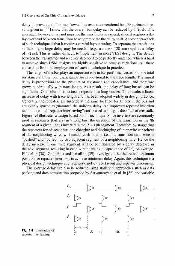
The length of the bus plays an important role in bus performances as both the totalresistance and the total capacitance are proportional to the trace length. The signaldelay is proportional to the product of resistance and capacitance, and thereforegrows quadratically with trace length. As a result, the delay of long busses can besignificant. One solution is to insert repeaters in long busses. This results a linearincrease of delay with trace length and has been adopted widely in design practice.Generally, the repeaters are inserted at the same location for all bits in the bus andare evenly spaced to guarantee the uniform delay. An improved repeater insertiontechnique called “repeater interleaving” can be used to mitigate the effect of crosstalk.Figure 1.4 illustrates a design based on this technique. Since inverters are commonlyused as repeaters (buffers) in a long bus, the direction of the transition in the lthsegment of a given line is inverted in the (l + 1)th segment. Therefore by staggeringthe repeaters for adjacent bits, the charging and discharging of inter-wire capacitorsof the neighboring wires will cancel each others, i.e., the transition on a wire is“pushed” and “pulled” by two adjacent segment of a neighboring wire. Hence thedelay increase in one wire segment will be compensated by a delay decrease inthe next segment, resulting in each wire charging a capacitance of 2CI on average.Elfadel in [38], Ghoneima and Ismail in [39] investigated the theoretical optimumposition for repeater insertions to achieve minimum delay. Again, this technique is aphysical design technique and requires careful trace layout and repeater placement.
The average delay can also be reduced using statistical approaches such as datapacking and data permutation proposed by Satyanarayana et al. in [86] and variable
Fig. 1.4 Illustration ofrepeater interleaving
L
2L 2L
di+2
di+1
di
di–1

8 1 Introduction of On-Chip Crosstalk Avoidance
cycle transmission proposed by Li et al. in [67]. All these techniques exploit thetemporal coherency of bus data to minimize the average delay for data transmission.Experimental results show significant improvements in the address bus case, withmore than 2.3× speedup reported in [86] and 1.6× speedup reported in [67]. Inthe case of a data bus, close to 1.5× speedup is reported. These techniques require2–6 additional wires. However, all statistical approaches require buffering capabilityon both the transmitter and receiver sides, to handle the non-deterministic delayvariation. The worst case delays remain unchanged.
Ho et al. in [45] and Schinkel et al. in [87] proposed using twisted differentialpairs for RC limited on-chip busses. A higher than 1 GHz data rate, with single-cyclelatency in a 10 mm on-chip wire in a 0.18-μm process was demonstrated in [45]. Thebus energy is also reduced duo to reduced signal swing. Schinkel et al. proposed anoffset differential structure as shown in Fig. 1.5 and reported a data rate up to 3 GHz[87]. Two major drawbacks of these approaches are the doubling of the number ofwires and the higher complexity and power consumption for both the differentialtransmitter and receiver designs.
Generally, capacitive coupling dominates the delay and power of an on-chip bus.However, on-chip inductive coupling cannot be ignored when the bus speed exceedsa certain limit. He et al. investigated the modeling of inductive crosstalk [42, 43]and they proposed several methods to control inductive crosstalk as well [42]. Theirmethods focused on a shield insertion and net ordering (SINO) algorithm that takesinto account inductive coupling. Several algorithms were proposed to achieve busdesigns that are either noise free (NF) or noise bounded (NB).
In addition to research in crosstalk avoidance for bus speed improvement, thereare also many publications focus on bus energy consumption reduction. The overallenergy consumption of any CMOS circuit is proportional to the total number oftransitions on the bus. The instantaneous power consumption on an N-bit bus atcycle i follows the general power dissipation equation by a CMOS circuit [91]
Pbus(i) =N∑
j=1
Cj · V2dd · f · pj(i) (1.1)
Fig. 1.5 Twisted differen-tial pairs with offset twists[45]
Tx–2
+
Tx–1
Tx0
Tx1
Rx–2
Rx–1
Rx0
Rx1

1.3 Bus Encoding for Crosstalk Avoidance 9
where N is the number of bits in the bus, Cj is the load capacitor on the jth line, Vdd
is the supply voltage, f the frequency and pj the activity factor at bit j. Assuming theCj = Cload for all j, the total energy consumption and average power of the bus is
Pbus(i) = Cload · V2dd · f · N(i) (1.2)
Pbus = Cload · V2dd · f · N (1.3)
where N(i) = ∑p( j) is the number of transitions at cycle i and N is the average
number of transitions per cycle. A reduction in the average power can be achievednot only by reducing C and Vdd , but also by lowering N .
In [65], Kim et al. proposed a coupling driven bus inversion scheme to reduce thetransitions on the bus. The basic idea of the scheme is to compute the total number oftransitions (including the coupling transitions) at a bus cycle, compare it to a giventhreshold and invert the bus when the total transition exceeds the threshold. Theyreported a 30% power saving on average.
In [85], Saraswat, Haghani and Bernard proposed using “T0” or “Gray Code” onbusses where data shows pattern regularity. A typical example is an address bus, sincethe data on an address bus typically changes at a regular increment. Neither codingschemes is suitable for general purpose busses with random data since the reductionin power in these schemes is highly dependent on the coherency of the data.
The effect of crosstalk on bus speed is not limited to on-chip busses. Crosstalk alsoimpacts off-chip bus performance. In addition to the differences in wire dimensions, amajor difference between on-chip and off-chip busses is that inductive coupling playsa more significant role in the overall crosstalk for off-chip busses. Part II presents acomprehensive discussion on off-chip bus crosstalk.
1.3 Bus Encoding for Crosstalk Avoidance
The majority of Part I is devoted to bus encoding related topics for on-chip buscrosstalk avoidance. Crosstalk avoidance bus encoding techniques manipulate theinput data before transmitting them on the bus. Bus encoding can eliminate certainundesirable data patterns and thereby reduce or eliminate crosstalk, with much lowerarea overhead than the aforementioned straightforward shielding techniques [36, 88,90, 99, 100]. These types of codes are referred to as crosstalk avoidance codes (CACs)or self shielding codes. Depends on their memory requirements, CACs can be furtherdivided into two categories: memoryless codes and memory-based codes. Memory-based coding approaches generate a codeword based on the previously transmittedcode and the current data word to be transmitted [34, 100]. On the receiver side, data isrecovered based on the received codewords from the current and previous cycles. Thememoryless coding approaches use a fixed code book to generate codewords to trans-mit. The codeword is solely dependent on the input data. The decoder in the receiveruses the current received codeword as the only input in order to recover the data.
Among all the memoryless CACs proposed, two types of codes have been heavilystudied. The first is called forbidden pattern free (FPF) code and the second type of
10 1 Introduction of On-Chip Crosstalk Avoidance
code has the property that between any two adjacent wires in the bus, there will be notransition in opposite directions in the same clock cycle. Different names have beenused in the literatures for the second type of codes. In this paper, we refer these codesas forbidden transition free (FTF) CACs. Both FPF-CACs and FTF-CACs yield thesame degree of delay reduction as passive shielding while requiring much less areaoverhead. Theoretically, the FPF-CAC has slightly better overhead performance thatthe FTF-CAC. In practice, for large size bus, this difference is negligible.
In this monograph, we also discuss some memory-based encoding techniques.Two such coding approaches are offered in this monograph: the “code pruning” andthe “ROBDD-based” method. Our theoretical analysis shows that memory-basedcodes offer improved overhead efficiency, compared to memoryless codes, and theexperimental results confirm this analysis.
Crosstalk avoidance codes cannot be put in practical use without efficient encoderand decoder (CODEC) implementations. We dedicate a portion of this monographto discussions of CODEC designs for CACs. We look at the impact of mappingschemes on the CODEC complexity. We present several CODEC designs that arehighly efficient compared to CODECs designs using conventional approaches. The“group complement” CODEC design uses bus partitioning to ensure low CODECcomplexity and high speed. Two CODEC designs based on the Fibonacci numeralsystem (FNS) achieve efficient area overhead while offering low complexity andhigh speed implementations.
Even though most of the codes and CODECs discussed in this monograph aredesigns for binary busses, we also investigate some crosstalk avoidance schemes formulti-valued busses and develop several encoding schemes for multi-valued bussesthat allows very low power and high speed bus interconnect. Study shows that themulti-valued busses are advantageous over the binary busses in many cases. Themonograph also addresses the the driver and receiver designs as they are often morechallenging than the binary drivers/receivers.
1.4 Part I Organization
The remainder of Part I is organized as follows: Chap. 2 provides physical and math-ematical models for bus signal delay and energy consumption, which account forcapacitive coupling between wires. Using these models, we establish a bus crosstalkclassification system. This classification system serves as the foundation for thesubsequent chapters. In Chap. 3, we discuss memoryless CACs, present designtechniques/algorithms to construct these codes, and provide the analysis and exper-imental results to compare their area overhead. Chapter 4 is dedicated to CODECdesigns for memoryless CACs. Several CODEC design techniques are presentedincluding “group complement”, a design technique based on bus partitioning, andseveral “Fibonacci Numeral System”-based designs. Through analysis and experi-ments we show that these CODEC designs are efficient in terms of area overhead,complexity and speed, compared to conventional schemes. In Chap. 5, we studymemory-based codes and show that these codes have better area overhead than

1.4 Part I Organization 11
memoryless approaches. Several code design algorithms are given in the chapteralong with experimental results to validate our analysis. Chapter 6 extends the ideaof crosstalk avoidance encoding to multi-valued busses. We first generalize the busclassification system to the multi-valued bus domain. We then present a bit-to-bitmapping scheme and two types of codes specifically designed for ternary busses.Experimental results are given to show that both coding schemes offer high speedand energy efficiency. We also discuss the challenges in bus driver and receiver cir-cuit designs in this chapter. Chapter 7 summarizes the work present in part I andoffers some insight on the directions for future work.

Chapter 2Preliminaries to On-Chip Crosstalk
This chapter provides background information and notation that will be needed forsubsequent chapters. Section 2.1 focuses on modeling of on-chip bus parasitics. Weshow the impact of wire dimensions and bus geometry on resistance and capacitance,and describe the equivalent circuit for the on-chip bus. We then derive the mathe-matical expression for both the signal delay and the energy consumption of a busbased on our models. In Sect. 2.2 we establish a bus classification system. This busclassification system serves as the foundation for the rest of this thesis.
2.1 Modeling of On-Chip Interconnects
Complementary metal-oxide-semiconductor (CMOS) on Silicon is the most com-monly used process for digital circuit design. Other processes include Siliconbipolar, GaAs, SiGe, Bi-CMOS or Silicon on insulator (SoI). The models builtin this work are based on CMOS process. However, all techniques discussed inthis part are technology independent, with minor differences arising from circuitimplementations.
The circuitry of a digital VLSI design is an assembly of gates and interconnects.Gates are the active circuits that implement logic operations. Interconnects are sim-ply conductors that connect the logic gates. Aluminum or copper are commonlyused to implement interconnect. Interconnects can be separated into local intercon-nects and global interconnects. Local interconnects generally refer to connectionsbetween gates within functional block. Global interconnects provide connections be-tween functional blocks. The length of local interconnects is relatively short. Globalinterconnects, on the other hand, can traverse the entire chip and be fairly long.
Interconnects introduce additional delay to the signals that travel through them[41, 68]. The delays of local interconnect can sometimes be significant but they arerelatively easier to deal with through physical layout, floorplanning, circuit re-timingor logic optimization.
Delays in global interconnect present a much greater challenge in high-perfor-mance designs. Because of their longer wire lengths (which can be as high as ten’s ofmillimeters), global interconnect delays are much larger than gate delays and local
C. Duan et al., On and Off-Chip Crosstalk Avoidance in VLSI Design, 13DOI 10.1007/978-1-4419-0947-3_2, © Springer Science+Business Media LLC 2010

14 2 Preliminaries to On-Chip Crosstalk
Fig. 2.1 3-D structure ofan on-chip conductor
L
T
W
interconnect delays. Global interconnects also contribute a large portion to the overallpower consumption. Lin pointed out in [41] that the total length of interconnects on achip can reach several meters and as much as 90% of the total delay in DSM designscan be attributed to global interconnects.
Figure 2.1 shows the 3-dimensional structure of a conductor (wire) that is used inVLSI interconnect. The length of the wire, L, is determined by the distance betweenthe components it connects and can be controlled by designers during the physicallayout. Even so, in large and complex designs, it may not be feasible to place allcomponents close to each other. The width of the wire, W , can also be adjustedduring physical layout. However, the minimum width, Wmin, is determined by thefabrication process. The height T is a constant for a given fabrication process andcannot be modified by the IC designers.
Even though other types of busses such as serial or asynchronous busses canbe used for on-chip interconnect, the majority of the digital VLSI circuits employsynchronous parallel busses due to their simplicity, good timing predicability andhigh throughput. A parallel global bus is typically implemented as a group of wiresrouted in parallel as shown in Fig. 2.2. The lengths of the wires are approximatelymatched. In practice, upper metal layers are used for global interconnects. In additionto W , T and L of individual wires, two more parameters are required to specify thebus: the spacing between wires, P, and the distance between the bus wires andthe substrate, H. Similar to Wmin, the minimum spacing Pmin is determined by thefabrication process and generally it can be assumed that Pmin = Wmin. In general,Pmin and Wmin are used whenever feasible to minimize the total area a bus occupies.For a given metal layer, H is also determined by the fabrication process.
For on-chip busses, two important electrical parameters of the wires of a bus arethe resistance R and the parasitic capacitance C. Their values are directly related tothe bus geometry. The resistance of a conductor is given as R = ρL
WT , where ρ is theresistivity of the material. Since ρ is determined by the material used for interconnects(Al or Cu), it is deemed fixed. To maintain low resistance of the conductors, we can

2.1 Modeling of On-Chip Interconnects 15
Fig. 2.2 A simplified 3-Dstructure of an on-chip bus
a
substrate
b c
H
P P
LT
W
choose materials with high conductivity, or vary bus geometry and wire dimensionsincluding W , L, and T . An increase in T and W results in lower resistance, so doesdecreasing L. However, as discussed previously, a small L can be attained throughfloorplanning in the layout stage, but is not always feasible in complex designs.Also, T is determined by the fabrication process and is not under designer’s control.Finally, increasing W increases the die area occupied by the bus.
The modeling of parasitic capacitance is less straightforward. There have beennumerous publications on accurate modeling and extraction of interconnect capac-itance using advanced methods such as finite difference, finite element, boundaryelement etc. [14, 25, 28, 94]. Interested readers can find a comprehensive overviewof interconnect capacitance modeling in [14]. We will only give some simplifiedmodels here.
Any two conductive surfaces (such as two wires in an on-chip bus, or a wireand the grounded substrate) form a capacitor. The capacitance is a function of thegeometries of the conductors. Two models that can be used to determine the capacitorbetween two parallel conductors: the parallel-plate capacitor model and the fringecapacitor model.
For a given wire in a bus, two dominant parasitic capacitance are the substratecapacitance and inter-wire capacitance. The substrate capacitor is formed between awire and the substrate and is denoted by CL . The inter-wire capacitance is a capacitorbetween two adjacent wires routed in parallel and is denoted by CI . There are otherparasitic capacitors beside CL and CI and in most cases they are negligible [14].For example, the overlap capacitance refers to the capacitance between wires ondifferent layers. In practice, wires on two adjacent layers are routed orthogonally(i.e., if on the k-th layer signals are routed North-South, then traces on the (k ± 1)-thlayers are routed East-West.). Also the coupling capacitance between two coplanar

16 2 Preliminaries to On-Chip Crosstalk
wires is negligible if these two wires are not adjacent to each other (because wiresin between act as shields which terminate the electrical field).
Using the model given in Fig. 2.2, it has been shown in [61] that to estimatethe capacitance between adjacent wires, the parallel-plate model is applicable whenT � P, where the capacitance can be expressed as CI = kε0
T ·LP . Here k is the
relative permittivity of the material and ε0 is the permittivity of free space. If T /P∼1or less, the fringing model applies and the capacitance is given as CI ∝ log(P).Similarly, to estimate the capacitance of a wire to the substrate, the parallel-platemodel is applicable if W � H, and CL = kε0
W ·LH . If W /H ∼1, then the fringing
model applies and CL ∝ log(H).For convenience of the ensuring discussion, we first define
λ = CI
CL. (2.1)
as the ratio of the inter-wire capacitance to the substrate capacitance. Once again λ
is a function of the bus geometry. For processes with feature size of 1 μm or greater,λ < 1, indicating that CI is negligible compared to the total capacitance. However,in DSM processes, λ � 1 [61] and CI contributes a dominant fraction of the totalcapacitance. Table 2.1 shows the technology evolution and the changes in the circuitgeometry. Table 2.2 lists the parasitic capacitance for the first 6 metal layers in 3different technologies. The parameters were extracted using a 3-D extraction toolspace3D [6] and based on a “strawman” model. The original work was conductedby Khatri in [61] and we were able to validate all the values independently.
Table 2.1 DSM process parameters [68]
Technology (μm) 0.25 0.18 0.15 0.13 0.09Vdd (V) 2.5 1.8 1.5 1.2 1Core gate oxide (Å) 50 32 26 20 16No. of metal layers 5 6 7 9 10Dielectric constant 4.1 3.7 3.6 2.9 2.9Metal pitch–M1(μm) 0.64 0.46 0.39 0.34 0.24Metal pitch–Others (μm) 0.8 0.56 0.48 0.41 0.28Resistivity–M1 (�−cm) 75 80 120 90 100Resistivity–N+/Poly (�/Ct) 7 8 13 11 20Resistivity–via (�/Ct) 4 7 9 1 1.5Ca (aF/μm) 15 11 11 15 14Cf (aF/μm) 10 8 8 11 9Cc (aF/μm) 80 90 97 105 94NMOS Vt (V) 0.53 0.42 0.42 0.28 0.27PMOS Vt (V) 0.53 0.5 0.42 0.42 0.32NMOS Idsat (μA/μm) 600 600 580 450 640PMOS Idsat(μA/μm) 270 270 260 270 280NMOS Ioff ( pA/μm) 10 20 35 320 500PMOS Ioff ( pA/μm) 1.5 2.5 40 160 500kgates/mm2 58 100 120 221 400Gate delay (ps) 40 32 20 17 12

2.1 Modeling of On-Chip Interconnects 17
Table 2.2 Parasitic capacitance (in pF/μm) at different metal layers in three different processes.All values were extracted using SPACE3D [61]
Technology 0.25 μm 0.10 μm 0.05 μm
Layers CL CI CL CI CL CI
1 10.96 40.76 9.97 49.35 15.75 46.822 0.86 27.79 0.92 48.05 1.64 47.583 1.77 40.92 2.58 45.84 5.38 48.284 0.96 41.83 1.10 44.08 1.2 46.665 2.02 23.36 2.31 39.84 3.90 39.156 10.27 33.48 1.07 40.59 1.51 38.33
Two equivalent circuits for data busses with parasitic resistance, RW , and parasiticcapacitance, CW , included are given in Fig. 2.3. The driver resistance is assumedto be RD. In Fig. 2.3a, the bus is modeled as a simple lumped RC network. Sucha model is accurate at low data rates and for moderate trace length. In general thismodel is accurate if the driver rise or fall times (τ ) is such that τ > RW CW . Asthe data rate goes up and the trace length becomes longer, the lumped RC modelbecomes inadequate and the bus needs to be modeled using a more sophisticated
V1 V2 V3 Vn-1 Vn
CI
RW
CL
CI
RD
CLCI
RD
CL
CI
RW
CLCI
RW
CL
CI
RD
CL
CI
RW
CLCI
RW
CLCI
RW
CL
CI
RW
CL
CI
RW
CL
CI
RW
CL
RW
CL RW
CL RW
CL
CI
CI
CI
R RRR
CI CI CI
CLCL CL CL
CI
V1 V2 V3 Vn
a
b
Fig. 2.3 Equivalent circuit for the data bus a Lumped RC model b Distributed RC model using2π -sections

18 2 Preliminaries to On-Chip Crosstalk
distributed RC network as shown in Fig. 2.3b. The condition for which a distributednetwork is required is τ < RW CW .
Accurate driver circuit modeling is also necessary in characterizing the bus be-havior. For now, we assume that busses for on-chip interconnects are binary andtherefore the driver only outputs two voltages representing logic high or logic low.The steady state voltage for logic high can be approximated as Vdd and that for logiclow as 0V. This assumption holds for most digital CMOS circuits.
In practice, bus drivers are typically implemented using inverters that are properlysized to meet the speed requirements of the bus. The maximum driver current isapproximately proportional to the gate width of the transistors of the driving inverter.Figure 2.4 shows the equivalent circuits of a driver in the output-high and the output-low states respectively. The driver is approximated as a resistor connected to Vdd or
Fig. 2.4 Equivalent circuitsfor the drivers a Vj highb Vj low
RDP
CI
CL
CI
Vj
Vj-1
Vj+1
VDD
RDN
CI
CL
CI
Vj
Vj-1
Vj+1
VDD
a
b

2.1 Modeling of On-Chip Interconnects 19
0V depends on the output logic state. In the output high state, the drive charges thecapacitors on the wire through a resistor with a resistance of RDP until the voltageon the line reaches Vdd . During the output-low, the capacitors on the bus wire isdischarged through a resistor with resistance of RDN . The value of RDP and RDN aredetermined by the transistor sizes of the driver and it can be assumed that the driversare sized so that RDP = RDN = RD. We also assume the all drivers in the samebus have the same sizes. In other words, all drivers of the same bus have a driverresistance of RD.
Using the equivalent circuits given in Figs. 2.3 and 2.4, we can derive the busenergy consumption expression. Let Er, j be the energy needed to drive the jth linein the bus from logic low to logic high, i.e. to charge all the capacitors on the jth linefrom 0V to Vdd . Let Ef , j be the energy needed to drive the jth line from logic lowto logic high, i.e. to discharge the capacitors from Vdd to 0V. Since no current flowsthrough Vdd in output-high state, we know
Ef , j ≡ 0. (2.2)
To compute the energy consumed to charge the bus in the output-high state, Er, j, weknow
Er, j =∫ t+
t−Vdd · Ij(t)dt (2.3)
where t− denotes the time before the transition, such that Vj(t−) = 0 and t+ denotesthe time after the transition when the steady state voltage is reached, i.e., Vj(t+) =Vdd . Vj(t) is simplified as Vj hereafter. Since
Ij(t) = CLdVj
dt+ CI
dVj, j−1
dt+ CI
dVj, j+1
dt(2.4)
where dVj, k = dVj − dVk . Now Eq. 2.3 can be rewritten as
Er, j =∫ t+
t−Vdd ·
(CL
dVj
dt+ CI
dVj, j−1
dt+ CI
dVj, j+1
dt
)dt
= CL · Vdd
∫ t+
t−dVj + CI · Vdd
∫ t+
t−dVj, j−1 + CI · Vdd
∫ t+
t−dVj, j+1
= CL · Vdd(�Vj + λ�Vj, j−1 + λ�Vj, j+1)
= (1 + 2λ − λδj, j−1 − λδj, j+1)CL · Vdd · Vj (2.5)
where
�Vj = Vj(t+) − Vj(t
−), (2.6)
�Vj, k = �Vj − �Vk , (2.7)
δj, k = sgn(�Vj)�Vk
Vdd, (2.8)

20 2 Preliminaries to On-Chip Crosstalk
δj, k is the normalized relative voltage change of the kth line with respect to the jthline, and δj, k ∈ {0, ±1}.
Equations 2.2 and 2.5 can be combined into a single expression
Ej = Er, j + Ef , j
= (1 + 2λ − λδj, j−1 − λδj, j+1)CL · V2dd · Vj
= ELj + EI
j
(2.9)
where ELj = CL · Vdd · Vj and EI
j = (2 − δj, j−1 − δj, j+1)λCL · Vdd · Vj. Equation2.9 can be interpreted as the total energy to drive a line and it can be expressed asthe sum of the energy to charge the substrate capacitor, EL
j , and the energy to chargethe inter-wire capacitors, EI
j . Equation 2.9 also shows that the energy consumptionis independent of RD and therefore the driver size.
For a bus, the total energy consumption is simply the summation of energy oneach individual line, and is expressed as follows
Etotal =N∑
j=1
Ej =N∑
j=1
ELj +
N∑
j=1
EIj . (2.10)
Again, the total energy can be separated into two portions: the energy to charge theload capacitors and the energy to charge the inter-wire capacitors.
To derive the signal delay for a bus with crosstalk, we first recall the derivationof the delay of a single wire when no inter-wire crosstalk is present. It is derived byfirst noting that the current flowing into CL and R is the same. Therefore in the outputhigh state, the current is
Ij(t) = CLdV (t)
dt= Vdd − V (t)
R(2.11)
It can be rewritten as
R · CL · dV (t) = (Vdd − V (t))dt (2.12)
Integration on both sides of Eq. 2.12, we get
R · CL
∫ V (τ )
0dV (t) =
∫ τ
0(Vdd − V (t))dt
R · CL · V (τ ) = Vdd · τ −∫ τ
0V (t)dt (2.13)
The solution to the differential equation Eq. 2.13 is
V (τ ) = Vdd(1 − e− τRC ) (2.14)
with the initial condition Vj(0) = 0V , the rise time to reach Vj(t) = αVdd is
τ (α) = −RC ln (1 − α) (2.15)

2.1 Modeling of On-Chip Interconnects 21
τ (0.5) = 0.69RC gives the rise time for the signal to reach the switching point (whichis typically 0.5Vdd for CMOS) and is generally used for the delay calculation. Otherrise time values of interest are τ (0.8) = 1.6RC and τ (0.9) = 2.3RC.
Based on the previous assumption that the drivers are properly sized to satisfyRD = RU = R, we can easily find out that the fall time for a logic high to logic lowtransition is the same as the rise times.
V (τ ) = Vdde− τRC (2.16)
τ (α) = −RC ln (α) (2.17)
When inter-wire capacitive crosstalk is included, Eqs. 2.11 and 2.12 become
CLdVj(t)
dt+ CI
dVj, j−1(t)
dt+ CI
dVj, j+1(t)
dt= Vdd − Vj(t)
R(2.18)
RCL · dVj(t) + RCI · dVj, j−1(t) + RCI · dVj, j+1(t) = (Vdd − Vj(t))dt (2.19)
Rewrite the left hand side of Eq. 2.19 as
RCL[dVj(t) + λ(2 · dVj(t) − Vj−1(t) − dVj+1(t))]
and perform integration on both sides, it becomes
RCL
∫[dVj(t) + λ(2 · dVj(t) − Vj−1(t) − dVj+1(t))] =
∫[Vdd − Vj(t)]dt (2.20)
To solve Eq. 2.20, dVj−1(t) an dVj+1(t) need to be known. Since all drivers andwires in a bus are identical, we can assume dVj+1(t) = δj, j+1dVj(t) and dVj−1(t) =δj, j−1dVj(t), where δj, k ∈ {0, ±1}. Here Eq. 2.20 can be simplified to
RCL
∫(1 + 2λ − λδj, j−1 − λδj, j+1)dVj(t) =
∫[Vdd − Vj(t)]dt. (2.21)
and the rise time can be derived in similar fashion as
τj(α) = −RCL(1 + 2λ − λδj, j−1 − λδj, j+1) ln (1 − α), (2.22)
and the 50% switch point delay is
τj(α) = −0.69RCL(1 + 2λ − λδj, j−1 − λδj, j+1). (2.23)
The fall time can be derived in similar fashion.
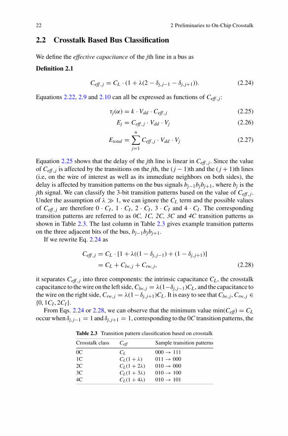
22 2 Preliminaries to On-Chip Crosstalk
2.2 Crosstalk Based Bus Classification
We define the effective capacitance of the jth line in a bus as
Definition 2.1
Ceff , j = CL · (1 + λ(2 − δj, j−1 − δj, j+1)). (2.24)
Equations 2.22, 2.9 and 2.10 can all be expressed as functions of Ceff , j:
τj(α) = k · Vdd · Ceff , j (2.25)
Ej = Ceff , j · Vdd · Vj (2.26)
Etotal =n∑
j=1
Ceff , j · Vdd · Vj (2.27)
Equation 2.25 shows that the delay of the jth line is linear in Ceff , j. Since the valueof Ceff , j is affected by the transitions on the jth, the ( j − 1)th and the ( j + 1)th lines(i.e, on the wire of interest as well as its immediate neighbors on both sides), thedelay is affected by transition patterns on the bus signals bj−1bjbj+1, where bj is thejth signal. We can classify the 3-bit transition patterns based on the value of Ceff , j.Under the assumption of λ � 1, we can ignore the CL term and the possible valuesof Ceff , j are therefore 0 · CI , 1 · CI , 2 · CI , 3 · CI and 4 · CI . The correspondingtransition patterns are referred to as 0C, 1C, 2C, 3C and 4C transition patterns asshown in Table 2.3. The last column in Table 2.3 gives example transition patternson the three adjacent bits of the bus, bj−1bjbj+1.
If we rewrite Eq. 2.24 as
Ceff , j = CL · [1 + λ((1 − δj, j−1) + (1 − δj, j+1)]
= CL + Clw, j + Crw, j, (2.28)
it separates Ceff , j into three components: the intrinsic capacitance CL , the crosstalkcapacitance to the wire on the left side, Clw, j = λ(1−δj, j−1)CL , and the capacitance tothe wire on the right side, Crw, j = λ(1−δj, j+1)CL . It is easy to see that Clw, j, Crw, j ∈{0, 1CI , 2CI }.
From Eqs. 2.24 or 2.28, we can observe that the minimum value min(Ceff) = CL
occur when δj, j−1 = 1 and δj, j+1 = 1, corresponding to the 0C transition patterns, the
Table 2.3 Transition pattern classification based on crosstalk
Crosstalk class Ceff Sample transition patterns
0C CL 000 → 1111C CL(1 + λ) 011 → 0002C CL(1 + 2λ) 010 → 0003C CL(1 + 3λ) 010 → 1004C CL(1 + 4λ) 010 → 101

2.2 Crosstalk Based Bus Classification 23
maximum values max(Ceff) = (1+4λ)CL occurs when δj, j−1 = −1 and δj, j+1 = −1,corresponding to the 4C patterns. Given that the signal delay τ is linear in Ceff , j,the classification system in Table 2.3 is also a classification system for the speed ofindividual bus wires.
For a parallel bus, the speed is determined by the worst case delay over all thebits in the bus. We can similarly classify the bus based on the worst case delay onany bit of the bus. As an example, suppose that 1101, 0010 and 1100 are transmittedon a 4-bit bus (b1b2b3b4) in cycle k, k + 1 and k + 2. The worst case delay is 4C onb3 during the transition from cycle k to k + 1. Such a bus is therefore classified as a4C bus.
A bus that transmits random data will experience maxj{Ceff , j} = (1 + 4λ)CL andtherefore the bus speed must be specified from Eq. 2.25 to accommodate the worstcase crosstalk delay, k · Vdd · CL(1 + 4λ). We refer to this as τ4C . In general, we referto the k · C crosstalk delay as τkC . Based on Table 2.3 and Eq. 2.25, we observe thatwhen λ � 1, by eliminating 4C crosstalk on ALL lines in the bus, we can increasethe maximum speed of the bus by ∼33%. If we can eliminate 3C AND 4C crosstalkon all lines, the bus can be sped up by ∼100%.
The analysis given above can be easily verified using circuit-level simulation. Weimplemented several bus circuits in SPICE [76] and verified the bus delay via circuitlevel simulations. The bus circuit was built using a BSIM4 [2] 0.1 μm process models.The traces are assumed to be routed on Metal4. All parasitic values were obtainedby a 3D parasitic extraction tool, SPACE3D [6] (and they match the data reportedin [61]). The distributed RC transmission line model shown in Fig. 2.3b was used.Table 2.4 reports the worst-case delays of bus signals. Column 1 lists the lengths of thebus wires. Column 2 reports the driver sizes in multiples of a minimum-sized driver(a minimum-sized driver in this case consists of a PMOS device with channel widthof 0.3 μm and a NMOS device with channel width of 0.1 μm. Columns 3–7 reportthe worst case delay of the bus in picoseconds, assuming that no greater than 0 · Cthrough 4 · C crosstalk patterns are allowed, respectively. A sample SPICE plot for thedelays of signals representing each of the 5 classes of crosstalk is shown in Fig. 2.5.
The delay values in Table 2.4 and Fig. 2.5 show that a bus which has 3C and 4Cpattern removed (e.g., by passive shielding) would reduce its worst case delay by
Table 2.4 Delay comparison (in ps) for different driver sizes and trace lengths
Trace length (mm) Buffer size 0c 1c 2c 3c 4c
5 30× 83 121 241 516 6655 60× 108 131 213 399 4025 120× 96 117 136 196 27910 30× 102 153 437 912 102610 60× 131 164 413 722 91910 120× 114 137 270 379 54820 30× 153 203 793 1068 158620 60× 164 206 691 1161 156120 120× 134 177 580 969 1365

24 2 Preliminaries to On-Chip Crosstalk
-0.5
0
0.5
1
1.5
0 1 2 3 4 5 6 7 8 ns
max delay vs. interwire capacitance
in0c1c2c3c4c
Fig. 2.5 Sample signal waveforms under different crosstalk conditions (60× driver, 2 cm tracelength, 0.1 μ process)
at least a factor of 2, regardless of bus trace length and driver strength. This resultsin significant savings for longer buses. Considering a 2 cm bus driven by a 60×minimum driver, the worst case delay would drop from 900 to 400 ps. All theseresults confirm our analysis that a bus can be sped up by avoiding certain undesirablecrosstalk classes. This is the foundation of the crosstalk avoidance bus encoding.
2.3 Bus Encoding for Crosstalk Avoidance
The basic operation of on-chip bus encoding for crosstalk avoidance is illustratedin Fig. 2.6. An n-bit input vector Vunc = b1b2 · · · bn is first encoded into an m-bitencoded vector, Venc = d1d2 · · · dm, which is transmitted over the bus. The receivedvector is decoded to recover the original data b1b2 · · · bn. The encoded data con-sists of specially designed codewords which guarantee that some high classes ofcrosstalk transition patterns never occur. By eliminating these classes of crosstalk
Encoder Driver Receiver Decodern-bit m-bit
m-bitm-bit n-bit
parallel buscodeworddata word codeword data word
Fig. 2.6 Bus encoding for crosstalk avoidance

2.4 Notation and Terminology 25
patterns, the bus can be operated at a higher speed, while consuming lower power.Such techniques to improve bus speed/power are referred to as Crosstalk AvoidanceEncoding techniques, and the encoded data are referred to as Crosstalk AvoidanceCodes (CACs).
Compared to an uncoded bus, a crosstalk avoidance encoded bus requires anencoder on the transmitter side and a decoder on the receiver side. The original datais the input to the encoder and is referred to as the data word, while the output of theencoder is referred to as the codeword in this thesis. The input to the decoder is thecodeword, and its output is the recovered data word.
Typically, the number of bits of the codewords is higher than that of the datawords,i.e., m > n. This is not always the case, however, as we will show in Chap. 6. Theadditional wires used for a coded bus are considered as area overhead because of theadditional routing space these wires occupy. The overhead percentage is defined asin Eq. 2.29. Note that the area of the encoder and decoder (CODEC) circuit are notincluded in the calculation of the area overhead. Instead, the encoder and decoder sizeare evaluated separately. This allows us to evaluate the code efficiency and CODECefficiency separately.
OH(n) = m − n
n(2.29)
In this monograph, we use the following set of rules as unified criteria to evaluatethe the performance of different CACs:
• Bus speedup: The ratio of the maximum speed of the coded bus to the maximumspeed of the uncoded bus.
• Area overhead: The ratio of the additional wires needed for the coded bus to thenumber of wires of the original uncoded bus.
• CODEC performance: This is quantified by measuring the complexity, powerconsumption and speed of the CODEC.
• Bus power: The power saving achieved by the coded bus compared to the uncodedbus.
2.4 Notation and Terminology
Except in Chap. 6, the following notations and terminologies are used unlessotherwise specified:
• V (n) denotes an n-bit binary vector. This is sometimes simplified as V . v denotesthe value of the vector V (n). vk denotes the value of the kth bit of V .
• b1b2 · · · bn−1bn (or bnbn−1 · · · b2b1) represents an n-bit uncoded input vector (dataword). bn is the most significant bit (MSB) and b1 is the least significant bit (LSB).
• d1d2 · · · dm−1dm (or dmdm−1 · · · d2d1) represents an m-bit coded vector (code-word). dm is the MSB and d1 is the LSB.
• A binary string represents the value of a vector. For example: 10101101 representsthe value of an 8-bit bus.

26 2 Preliminaries to On-Chip Crosstalk
• In the case of bus partitioning, a vector V is divided into multiple “groups”. Subsc-ripts are used to denote group number. For example. either (d1d2d3d4)1(d1d2d3d4)2or d1,1d1,2d1,3d1,4d2,1d2,2d2,3d2,4 are used to indicate an 8-bit vector partitionedinto two groups of 4-bits. (1011)1(0101)2 means that the patterns in the 1st and2nd group are 1011 and 0101 respectively.
• If necessary, superscripts are used to denote the cycle number. For example,(10101101)k is the value of the bus in the kth cycle.
• “→” denotes a transition. For example, (10101)k → (01001)k+1 indicates thatthe bus pattern transitions from 10101 in the kth cycle to 01001 in the (k + 1)thcycle.
• “⇒” is an operator that denotes an encoding process. For example, a 3-bit to 4-bitencoding is expressed as b1b2b3 ⇒ d1d2d3d4.

Chapter 3Memoryless Crosstalk Avoidance Codes
Memoryless codes are a class of CACs in which data words and codewords have a1-to-1 mapping. The encoder uses a fixed codebook and it output is independent ofthe previously transmitted codewords, hence memoryless.
In this chapter, we present several different types of memoryless codes. Thesecodes offer various degrees of crosstalk reduction that result in a bus speed-up rangingfrom 100% to over 400%. For each code, we will discuss in detail the code designand quantify its characteristics in terms of speed and area overhead.
3.1 3C-Free CACs
3C-free memoryless CACs ensure that 4C and 3C crosstalk transitions are eliminatedfrom the bus. They are by far the most popular CACs and have been heavily studiedin the literature [36, 81, 89, 90, 99, 100]. The bus speed-up they offer is equivalent topassive shielding. In fact, passive shielding can be treated as a 3C-free memorylessencoding, b1b2 · · · bn−1bn ⇒ b10b20 · · · 0bn−10bn. As we will show in this chapter,3C-free CACs offer power saving. In addition, Raghunandan et al. pointed out that3C-free codes also offers added robustness to process variation [81].
3C-free CACs eliminate all 3C and higher crosstalk patterns in the m-bit bus,and thus satisfy maxj(Ceff, j) = (1 + 2λ)CL . From Eq. 2.25, if we assume λ � 1,we know that τ4C ≈ 2 · τ2C . Therefore the maximum speed of a 3C-free bussesis approximately doubled compared to an uncoded bus of the same configuration.Using the actual delay numbers given in Table 2.4, we see that the maximum signaldelay on a 20 mm bus with 60× size drivers is reduced from 1561 to 691 ps if 3C-free encoding is applied. As a result, the maximum speed of such a coded bus is∼1.44 GHz, 125% faster than an uncoded bus.
In the following sections, two types of 3C-free memoryless CACs are discussed:the Forbidden Pattern Free codes and the Forbidden Transition Free codes. Wewill show that even though these codes are designed based on different principles,their area overhead are very similar. Both types of codes are considered highlyefficient.
C. Duan et al., On and Off-Chip Crosstalk Avoidance in VLSI Design, 27DOI 10.1007/978-1-4419-0947-3_3, © Springer Science+Business Media LLC 2010

28 3 Memoryless Crosstalk Avoidance Codes
3.1.1 Forbidden Pattern Free CAC
The forbidden pattern free codes are the most area overhead efficient 3C-free memoryCACs [36]. These codes guarantee that transitions between any two codewords satisfy2−δj, j−1−δj, j+1 < 3 for all bits. The detailed design of the code and its performanceanalysis are given as follows.
3.1.1.1 Code Design
Definition 3.1 Forbidden patterns are 3-bit binary patterns vj−1vjvj+1 that satisfyvj−1 = vj+1 = vj.
The only patterns that satisfy Definition 3.1 are 010 and 101.
Definition 3.2 A vector that contains no forbidden pattern in any three consecutivebits is a forbidden-pattern-free (FPF) vector.
For example, 11100110 and 11000110 are FPF vectors, 11010011 and 11110110are not FPF vectors.
Theorem 3.1 If all vectors in a set are forbidden pattern free, transitions amongthese vectors satisfy maxj(Ceff , j) = 2 × CI .
Theorem 3.1 states that if forbidden patterns are not allowed on the bus, thenmax(Ceff ) = 2 × CI , i.e., the bus is 3C-free.
It is possible to prove Theorem 3.1 by an exhaustive examination of all transitionpatterns. The following gives the mathematical proof.
Proof We prove that both 4C and 3C transitions require forbidden patterns ondj−1djdj+1. Let the bit patterns be vk
j−1vkj vk
j+1 and vk+1j−1 vk+1
j vk+1j+1 in the kth and
(k + 1)th cycles respectively.
• From Eq. 2.24, we know that for Ceff , j = 4 × CI , it is required that δj, j−1 = −1and δj, j+1 = −1, i.e., vj−1 and vj transit in opposite directions and vj and vj+1transit in opposite directions. We have the following logical relations:
– vkj−1 = vk
j ,
– vkj−1 = vk+1
j−1 ,
– vkj = vk+1
j ,
– vkj+1 = vk+1
j+1 and
– vkj+1 = vk
j
and these logic relations result in vkj−1 = vk
j = vkj+1 and vk+1
j−1 = vk+1j = vk+1
j+1 . Soin both cycles forbidden patterns appear on dj−1djdj+1.
• From Eq. 2.24, for Ceff , j = 3 × CI , it is required that δj, j−1 = −1 and δj, j+1 = 0,or δj, j−1 = 0 and δj, j+1 = −1. Without loss of generality, we assume the formercase and have

3.1 3C-Free CACs 29
– vkj−1 = vk
j ,
– vkj−1 = vk+1
j−1 ,
– vkj = vk+1
j and
– vkj+1 = vk+1
j+1
If vkj+1 = vk
j , we will have vk+1j−1 = vk+1
j = vk+1j+1 . If vk
j+1 = vkj , we have
vkj−1 = vk
j = vkj+1. Therefore, a forbidden pattern appears either in the kth cycle
or in the (k + 1)th cycle.
Combining both cases, we know that by eliminating forbidden patterns on the bus,it is guaranteed that no 4C or 3C transition remain on the bus and max(Ceff ) = 2×CI .
To generate a complete set of m-bit FPF codewords, a simple-minded approachis to remove all codewords that contains forbidden patterns from the 2m entries.However, such an exhaustive search approach is impractical when m is large. Instead,the FPF-CAC can be generated using an inductive procedure [36].
Let Sm be the set of m-bit FPF-CAC codewords and let m-bit vector Vm =dmdm−1 · · · d1 be a codeword. Any codeword Vm ∈ Sm can be considered as theconcatenation of Vm−1 = dm−1dm−2 · · · d1 with bit dm, where Vm−1 ∈ Sm−1. Theallowed values on dm is determined by dm−1dm−2. For example, if dm−1dm−2 = 00or dm−1dm−2 = 11, then dm can be either 0 or 1. If dm−1dm−2 = 10, dm can only be0 as dm = 1 will introduce a forbidden pattern, 010, on dmdm−1dm−2.
This idea is utilized in the inductive procedure that generates FPF codewords,given in Algorithm 3.1.
Algorithm 3.1 FPF codeword generation
S2 = {00, 01, 10, 11}for m ≥ 3 do
Sm = ∅;for ∀Vm−1 ∈ Sm−1 do
if dm−1dm−2 = 00 or 11 thenadd 0 · Vm−1 and 1 · Vm−1 to Sm;
else if dm−1dm−2 = 01 or 10 thenadd dm−1 · Vm−1 to Sm;
end ifend for
end for
“·”: concatenation operator
Table 3.1 lists the codewords of the 3, 4 and 5 bit FPF-CACs generated byAlgorithm 3.1.
An uncoded n-bit bus has 2n distinct vectors. For an m = n + r bit bus, thereare Tg(m) vectors that are forbidden pattern free. It is necessary that Tg(m) ≥ 2n be

30 3 Memoryless Crosstalk Avoidance Codes
Table 3.1 FPF-CAC codewords for 2, 3, 4 and 5-bit busses
2-bit 3-bits 4-bits 5-bit
00 000 0000 00000 1000001 001 0001 00001 1000110 011 0011 00011 1001111 100 0110 00110 11000
110 0111 00111 11001111 1000 01100 11100
1001 01110 111101100 01111 1111111101111
satisfied so that we can map each input (n-bit) vector uniquely to one distinct output(m-bit) vector that is an FPF vector. To minimize the area overhead, for a given inputbus size, n, we want to find the smallest m so that Tg(m) ≥ 2n is satisfied.
The code cardinality, Tg(m), determines the area overhead and therefore is animportant parameter in evaluating the code performance. The next section shows thecomputation of FPF code cardinality.
3.1.1.2 Code Cardinality
From Algorithm 3.1, we can see that for each m − 1 bit codeword Vm−1 ∈ Sm−1with last two digits dm−1 = dm−2, two m-bit codewords can be generated. For Vm−1with the last two digits bm−1 �= bm−2, only one m-bit codeword can be generated.The total number of FPF-CAC codewords can be computed based on the followingequations:
Definition 3.3 For an m-bit vector dmdm−1 . . . d2d1, we define the following quan-tities:
• T (m) is the total number of distinct m-bit vectors.• Tg(m) is the total number of FPF vectors.• Tb(m) is the total number of non FPF vectors.• Tgg(m) is the number of FPF vectors satisfy dm = dm−1.• Tgb(m) is the number of FPF vectors satisfy dm �= dm−1.
For the base case, a 3-bit bus: (m = 3)
T (3) = 8,
Tg(3) = 6,
Tg(3) = 2,
Tgg(3) = 4,
Tgb(3) = 2

3.1 3C-Free CACs 31
For busses with more than 3-bits: (m > 3)
Tg(m) = 2 × Tgg(m − 1) + Tgb(m − 1) (3.1)
Tgg(m) = Tgg(m − 1) + Tgb(m − 1) (3.2)
Tgb(m) = Tgg(m − 1) (3.3)
Based on Algorithm 3.1 and the definitions of Tg, Tgg and Tgb, we get
Tg(m) = Tgg(m) + Tgb(m) (3.4)
Tgg(m) = Tg(m − 1) (3.5)
and Eq. 3.1 can be re-written as
Tg(m) = 2 × Tgg(m − 1) + Tgb(m − 1)
= (Tgg(m − 1) + Tgb(m − 1)) + Tgg(m − 1)
= Tg(m − 1) + Tg(m − 2) (3.6)
The relationship shown in Eq. 3.6 is the same as the relationship of elements in theFibonacci sequence.1 With the initial conditions Tg(2) = 4 = 2 · f3 and Tg(3) = 6 =2 · f4, we have
Tg(m) = 2 · fm+1 (3.7)
where fm is the mth element in the Fibonacci sequence [3].Tg(m) gives the maximum cardinality of the m-bit FPF-CAC code. To encode an
n-bit binary bus into FPF-CAC code, the minimum number of bits needed mopt isthe smallest integer m that satisfies Eq. 3.8.
n ≤ �log2 (2 · fm+1)� (3.8)
The mth Fibonacci number can be expressed as
fm = (−ϕ)m − (1 − ϕ)m
√5
, (3.9)
where ϕ = 1.618 is also known as the golden ratio. ϕ is also the asymptotic ratio oftwo consecutive elements of the sequence and ϕ = limk→∞ fk+1
fk. For large busses,
the lower bound of the area overhead based on Eq. 2.29 is
min(OH(n)) = m − n
n≥ 1
log2 ϕ− 1 ≈ 44% (3.10)
Figure 3.1 plots min(OH(n)) for bus size from 3 to 86 and shows that it asymptoticallyapproaches 44%.
1 A more detailed discussion about Fibonacci sequence will be given in Chap. 4.

32 3 Memoryless Crosstalk Avoidance Codes
Fig. 3.1 Percentageoverhead
0 10 20 30 40 50 60 70 80 900.25
0.3
0.35
0.4
0.45
0.5Overhead Percentage
Input Buswidth
If we define the coding gain of a CAC, G(n), as the gain of throughput per unitarea of the coded bus over the uncoded bus, it can be expressed as
G(n) = Renc · n
Runc · m− 1 (3.11)
where Renc is the data rate of the encoded bus and Runc is the data rate of the uncodedbus. In the case of 3C-free codes, Renc ≈ 2 × Runc. Therefore, the coding gain of theFPF code is
GFPF ≈ 39%.
Note that the coding gain of a shielding scenario is 0.
3.1.2 Forbidden Transition Free CAC
The forbidden transition free CAC (FTF-CAC) is another efficient 3C-free memory-less code. It was first proposed by Victor and Keutzer in 2001 [100], and is reviewedin this section since we will use the FTF CAC to derive an efficient CODEC inSect. 4.5. The basic idea of the FTF code is to prohibit two adjacent bits from tran-sitioning in opposite directions, i.e., the forbidden transitions 01 → 10 or 10 → 01are not allowed. This guarantees that δj, j+1 ≥ 0, therefore (2 − δj, j−1 − δj, j+1) ≤ 2and the bus satisfies maxj(Ceff, j) = 2. Hence the transition is 3C-free. An FTF codeis a set of codewords such that transitions among these codewords do not produceforbidden transitions on any two adjacent bits.

3.1 3C-Free CACs 33
3.1.2.1 Code Design
A forbidden transition is defined as the simultaneous transition (in opposite direc-tions) on two adjacent bits, i.e., 01 → 10 or 10 → 01. In the literature, two adjacentbits are sometimes referred to as a boundary and we will use this terminology here-after. We first observe that to guarantee forbidden transition freedom on the boundarydjdj+1 between any two codewords in an FTF-CAC, the 01 and 10 patterns cannotcoexist in the same set of codewords. This can be easily confirmed by examining thetransitions among codes in {00, 01, 11}, or {00, 10, 11}. If we eliminate 01 OR 10from all the boundaries in the codewords in a set of codewords R, we can guaranteethat R is forbidden transition free. Therefore, once again, the problem of elimi-nation forbidden transitions is transformed into a problem of eliminating specificpatterns.
Theorem 3.2 The largest sets of codewords satisfying the forbidden transition freecondition is the set of codewords that can transition to a class 1 codeword (defined asa codeword with alternating 0 and 1 bits) without generating forbidden transitions.
The proof of Theorem 3.2 can be found in [100] and will not be repeatedhere. For any given size bus, there are two class 1 codewords: “1010 . . .” and“0101 . . .”. From Theorem 3.2, we can see that there exist two different sets withthe same maximum cardinality. In one set (set A), in all codewords, the 01 pattern iseliminated from d2j+1d2j boundaries and the 10 pattern is eliminated from d2jd2j−1boundaries. In the second set (set B), the 10 pattern is eliminated from d2j+1d2j
boundaries and the 01 pattern eliminated from d2jd2j−1 boundaries. This is differentfrom the FPF code, which has one unique set with maximum cardinality for eachbus width.
Table 3.2 lists all set A FTF codewords for 2, 3, 4 and 5-bit busses. Take the 5-bitbus as an example, we can see that 10 is not present in d2d1 and d4d3, and 01 is notpresent in the boundaries d3d2 and d5d4. If one of these two sets is known, the otherset can be produced by simply complementing all the codewords in the first set.
There are multiple methods to produce all the n-bit codewords in the set thatsatisfy Theorem 3.2.
• Start with a complete set of 2n vectors and remove codewords that do not satisfythe boundary constraints.
Table 3.2 FTF-CAC codewords for 2, 3, 4 and 5-bit busses
2-bit 3-bits 4-bits 5-bit
00 000 0000 00000 1010001 001 0001 00001 1010111 100 0100 00100 10111
101 0101 00101 11100111 0111 00111 11101
1100 10000 111111101 100011111

34 3 Memoryless Crosstalk Avoidance Codes
• Start with a set consisting of a single class 1 codeword and grow the FTF-CACcodewords by adding compatible codewords to the set.
• Start from a small FTF set (say 2-bit FTF codes) and inductively append bits tothe codewords in the set until the codeword length reaches n-bits.
Clearly, the first (pruning) method is impractical when n is large, since a completeset of codewords have 2n entries and searching through n − 1 boundaries requiresO(2(n−1)n) searches.
Both the second and the third methods listed above actually “grow” the FTFcodewords instead of “pruning”, and therefore require less computation. The methodof “growing” codewords by appending bits to codewords in an existing set is similarto the FPF codeword generation algorithm given in Algorithm 3.1. Algorithm 3.2 isthe pseudo code for generating the FTF codewords.
Algorithm 3.2 FTF codeword generation
S2 = {00, 01, 11}for m > 2 do
if m is odd thenfor ∀Vm−1 ∈ Sm−1 do
add 1 · Vm−1 to Sm;if dm−1 = 0 then
add 0 · Vm−1 to Sm;end if
end forelse
for ∀Vm−1 ∈ Sm−1 doadd 0 · Vm−1 to Sm;if dm−1 = 1 then
add 1 · Vm−1 to Sm;end if
end forend if
end for
3.1.2.2 Code Cardinality
The inductive codeword generation method given in Algorithm 3.2 can be used toderive the cardinality of the FTF codes. We first define
Definition 3.4
Tt(m) : number of m-bit FTF vector,
Tt1(m) : number of m-bit FTF vector with the MSB being 1,
Tt0(m) : number of m-bit FTF vector with the MSB being 0.
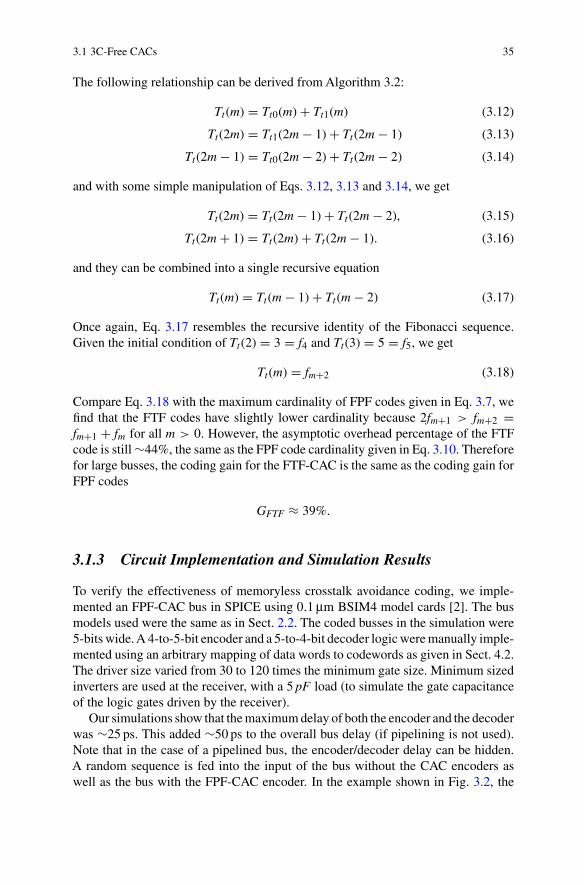
3.1 3C-Free CACs 35
The following relationship can be derived from Algorithm 3.2:
Tt(m) = Tt0(m) + Tt1(m) (3.12)
Tt(2m) = Tt1(2m − 1) + Tt(2m − 1) (3.13)
Tt(2m − 1) = Tt0(2m − 2) + Tt(2m − 2) (3.14)
and with some simple manipulation of Eqs. 3.12, 3.13 and 3.14, we get
Tt(2m) = Tt(2m − 1) + Tt(2m − 2), (3.15)
Tt(2m + 1) = Tt(2m) + Tt(2m − 1). (3.16)
and they can be combined into a single recursive equation
Tt(m) = Tt(m − 1) + Tt(m − 2) (3.17)
Once again, Eq. 3.17 resembles the recursive identity of the Fibonacci sequence.Given the initial condition of Tt(2) = 3 = f4 and Tt(3) = 5 = f5, we get
Tt(m) = fm+2 (3.18)
Compare Eq. 3.18 with the maximum cardinality of FPF codes given in Eq. 3.7, wefind that the FTF codes have slightly lower cardinality because 2fm+1 > fm+2 =fm+1 + fm for all m > 0. However, the asymptotic overhead percentage of the FTFcode is still ∼44%, the same as the FPF code cardinality given in Eq. 3.10. Thereforefor large busses, the coding gain for the FTF-CAC is the same as the coding gain forFPF codes
GFTF ≈ 39%.
3.1.3 Circuit Implementation and Simulation Results
To verify the effectiveness of memoryless crosstalk avoidance coding, we imple-mented an FPF-CAC bus in SPICE using 0.1 μm BSIM4 model cards [2]. The busmodels used were the same as in Sect. 2.2. The coded busses in the simulation were5-bits wide. A 4-to-5-bit encoder and a 5-to-4-bit decoder logic were manually imple-mented using an arbitrary mapping of data words to codewords as given in Sect. 4.2.The driver size varied from 30 to 120 times the minimum gate size. Minimum sizedinverters are used at the receiver, with a 5 pF load (to simulate the gate capacitanceof the logic gates driven by the receiver).
Our simulations show that the maximum delay of both the encoder and the decoderwas ∼25 ps. This added ∼50 ps to the overall bus delay (if pipelining is not used).Note that in the case of a pipelined bus, the encoder/decoder delay can be hidden.A random sequence is fed into the input of the bus without the CAC encoders aswell as the bus with the FPF-CAC encoder. In the example shown in Fig. 3.2, the

36 3 Memoryless Crosstalk Avoidance Codes
waveform w/o encoder
–4.00E–01
–2.00E–01
0.00E+00
2.00E–01
4.00E–01
6.00E–01
8.00E–01
1.00E+00
1.20E+00
1.40E+00
1.60E+00
0 2 4 6 8 10 12 14 16 18 20
Vtx1 Vtx2 Vtx3 Vtx4 Vtx5
0 2 4 6 8 10 12 14 16 18
waveform w/ coding
–5.00E-01
0.00E+00
5.00E–01
1.00E+00
1.50E+00
2.00E+00
Vin1 Vseg1 Vseg2 Vseg3 Vseg4 Vseg5
a
b
Fig. 3.2 Bus signal waveforms. Bus is 20 mm long and the driver size is 60× the minimum size,implemented in a 0.1 μm process a Signal waveform on the bus without coding b Signal waveformon the bus with coding
bus lengths are 20 mm and the driver sizes are 60×. The results from the sim-ulation match our theoretical analysis very well. The signal waveforms for anuncoded 4-bit bus in Fig. 3.2a show a worse case delay (from the 50% point atthe input of the encoder to the point the bus voltage reaches 50% of Vdd at the re-ceiver gates) that is greater than 1000 ps. On the coded bus shown in Fig. 3.2b, the

3.2 2C-Free CACs 37
–2.00E-01
0.00E+00
2.00E–01
4.00E–01
6.00E–01
8.00E-01
1.00E+00
1.20E+00
1.40E+00
Voo1Voo2Voo3Voo4Voo5
0 2 4 6 8 10 12 14 16 18
0 4 6 8 14 16
–2.00E–01
0.00E+00
2.00E–01
4.00E–01
6.00E–01
8.00E–01
1.00E+00
1.20E+00
1.40E+00
rcv1rcv2rcv3rcv4rcv5
12
a
b
102
Fig. 3.3 Signal waveforms at the receiver output. Bus is 20 mm long and the driver size is 60×the minimum size, implemented in 0.1 μm process a Receiver output waveform on the bus withoutcoding b Receiver output waveform on the bus with coding
delay is less than 500 ps. The delay variations are ∼1000 and ∼500 ps respectively.Figure 3.3 shows the reshaped output signals of the receivers. The edge jitter in theuncoded bus and the coded bus are ∼1000 and ∼500 ps respectively. The resultsindicate that the maximum data rate on the uncoded bus cannot exceed 1 Gbpswhile a coded bus can operate faster than 2 Gbps, more than doubling the busspeed.
3.2 2C-Free CACs
2C-free codes satisfy maxj(Ceff , j) = (1 + λ)CL and therefore a 2C-free bus can besignificantly faster than a 3C-free bus of the same configuration. Using the valuesfrom Table 2.4, a 20 mm 2C-free bus with 60× drivers can operate at 4.8 GHz, 7.57×

38 3 Memoryless Crosstalk Avoidance Codes
as fast as an uncoded 4C bus, or 3.35× as fast as a 3C-free bus. The 2C-free codes,however, require larger area overhead as shown in the following sections.
3.2.1 Code Construction
Let Qn be an n-bit 2C-free clique (a set of codewords). To satisfy the condition thattransitions between any two codewords in the clique are 2C-free (i.e., maxj(Ceff , j) =(1 + λ)CL), we know that Clw, j ≤ 1CI and Crw, j ≤ 1CI based on Eq. 2.28, and alsoClw, j and Crw, j cannot be 1CI at the same time. Using these criteria, we can examinethe properties of all codewords Vn ∈ Qn.
Again we first examine the 3-bit slice dj−1djdj+1. We know that “01” and “10”cannot both exist in dj−1dj boundary as it would violate Clw, j ≤ 1CI . Without lossof generality, let us assume that all the valid patterns on dj−1djdj+1 are in forms of00×, 11× or 01×. The value of dj+1, vj+1, shall be chosen based on the followingobservations:
• if vj+1 = vj, the patterns are 000, 111, 011. This satisfy the 2C-free requirement.This forms a base clique.
• 010 is not compatible2 with elements in the base clique, 000 and 111.• 110 can be added to the clique and the expanded clique {000, 111, 011, 110} is
still 2C-free.• 001 has a 2C transition with 011, which is an element in the base clique. It is
compatible with other elements in the clique.
An inductive codeword generation method can be developed based on these obser-vations. Suppose an n-bit 2C-free clique Qn is available to us, let the (n + 1)-bit 2Ccrosstalk free clique be initialized to the empty set. We then add n+1-bit codewordsbased on the compatibility requirement as shown in Algorithm 3.3.
Algorithm 3.3 Construction of Qn+1 from Qn
Q3 = {000, 111, 011, 110};T (n) = 4;T00(n) = 1; T01(n) = 0; T10(n) = 1; T11(n) = 2;Qtype = 10;for next n do
Qn+1 = ∅;Qn+1 = Qn
⋃Vn · vn, ∀Vn ∈ Qn;
T (n + 1) = T (n);T00(n + 1) = T00(n) + T10(n);T11(n + 1) = T11(n) + T01(n);T01(n + 1) = 0; T10(n + 1) = 0;if Qtype = 10 then
2 By compatible, we mean that two vectors have a non 2C-free transition.

3.2 2C-Free CACs 39
Qn+1 = Qn⋃
Vn,00 · 1, ∀Vn,00 ∈ Qn;T01(n + 1) = T00(n); T (n + 1) = T (n + 1) + T00(n);Qtype = 01;
elseQn+1 = Qn
⋃Vn,11 · 0, ∀Vn,11 ∈ Qn;
Qtype = 10;T10(n + 1) = T11(n); T (n + 1) = T (n + 1) + T11(n);
end ifend for
The pseudo-code is given in Algorithm 3.3. The clique type, Qtype, is “01” when01 is present in the last two bits of the codewords in the set. Conversely, Qtype = 10when 01 is present in the boundary. T (n) is the cardinality of Qn and Txy(0) is thenumber of vectors ending with xy in Qn. Note that if Qtype is “01”, (i.e., T10(n) = 0),the new clique, Qn+1, derived based on Algorithm 3.3 is of “10” type and thereforedoes not contain vectors with dndn+1 = 10.
Using the inductive procedure given in Algorithm 3.3, we can produce cliquesof arbitrary bus sizes. The procedure, however, does not necessarily yield a 2C-freeclique with maximal cardinality. As we pointed out earlier, vectors Vn,00 ·1 and V01 ·1are not compatible, neither are Vn,11 · 0 and Vn,10 · 0. In Algorithm 3.3 we do not addvectors of Vn,00 · 1 and Vn,11 · 0 in the new clique whenever the incompatibility isdetected. However, if Vn,01 · 1 vectors are not in the new clique, we can add Vn,00 · 1vectors into Qn+1 instead. Similarly, we can add Vn,11 · 0 vectors instead Vn,10 · 0vectors into Qn+1. Note that the number of Vn,01 · 1 vectors is T01(n) and the numberof Vn,00 · 1 vectors is T00(n). To maximize the size of the new clique, we shouldselect the set with larger number of vectors. The same principle applies to the setsof Vn,10 · 0 vectors and Vn,11 · 0 vectors. Algorithm 3.4 gives the modified inductivecodeword generation procedure.
Algorithm 3.4 Modified inductive procedure to construct Qn+1 to maximizethe clique size
Q3 = {000, 111, 011, 110};T (n) = 4;T00(n) = 1; T01(n) = 0; T10(n) = 1; T11(n) = 2;Qtype = 10;for next n do
Qn+1 = ∅;Qn+1 = Qn
⋃Vn,00 · 0, ∀Vn,00 ∈ Qn;
Qn+1 = Qn⋃
Vn,11 · 1, ∀Vn,11 ∈ Qn;T (n + 1) = T00(n) + T11(n);T00(n + 1) = T00(n);T11(n + 1) = T11(n);T01(n + 1) = 0; T10(n + 1) = 0;

40 3 Memoryless Crosstalk Avoidance Codes
if Qtype == 00 thenif T00(n) > T11(n) then
Qn+1 = Qn⋃
Vn,00 · 1, ∀Vn,00 ∈ Qn;T01(n + 1) = T00(n); T (n + 1) = T (n + 1) + T00(n);Qtype = 01;
elseQn+1 = Qn
⋃Vn,11 · 0, ∀Vn,11 ∈ Qn;
T10(n + 1) = T11(n); T (n + 1) = T (n + 1) + T11(n);Qtype = 10;
end ifelse if Qtype == 10 then
if T00(n) > T01(n) thenQn+1 = Qn
⋃Vn,00 · 1, ∀Vn,00 ∈ Qn;
T01(n + 1) = T00(n); T (n + 1) = T (n + 1) + T00(n);Qtype = 01;
elseQn+1 = Qn
⋃Vn,01 · 1, ∀Vn,01 ∈ Qn;
T11(n + 1) = T01(n); T (n + 1) = T (n + 1) + T01(n);Qtype = 00;
end ifelseif T11(n) > T10(n) then
Qn+1 = Qn⋃
Vn,11 · 0, ∀Vn,11 ∈ Qn;Qtype = 10;T10(n + 1) = T11(n); T (n + 1) = T (n + 1) + T11(n);
elseQn+1 = Qn
⋃Vn,00 · 1, ∀Vn,00 ∈ Qn;
T00(n + 1) = T10(n); T (n + 1) = T (n + 1) + T10(n);Qtype = 00;
end ifend if
end for
3.2.2 Code Cardinality and Area Overhead
For the procedure given in Algorithm 3.3. We have
T00(n + 1) ={
T00(n) + T10(n), if T01(n) = 0,T00(n),otherwise
(3.19)
T11(n + 1) ={
T11(n), if T01(n) = 0,T11(n) + T01(n), otherwise
(3.20)
3.2 2C-Free CACs 41
T01(n + 1) ={
T00(n), if T01(n) = 0,0, otherwise
(3.21)
T10(n + 1) ={0, if T01(n) = 0,T11(n), otherwise
(3.22)
Assume Qtype(n) is “10”, i.e. T01(n) = 0, according to Algorithm 3.3, bothQtype(n + 1) and Qtype(n − 1) are “01”. Equations 3.19, 3.20, 3.21 and 3.22 canbe simplified into
T00(n + 1) = T00(n − 1) + T11(n − 1) (3.23)
T11(n + 1) = T11(n − 1) + T01(n − 1)
= T11(n − 1) + T00(n − 3) (3.24)
T01(n + 1) = T00(n − 1) (3.25)
T10(n + 1) = 0. (3.26)
and we also have
T (n + 1) = T00(n + 1) + T11(n + 1) + T01(n + 1) + T10(n + 1)
= T00(n − 1) + T11(n − 1) + T11(n − 1) + T01(n − 1) + T00(n − 1)
= 2 · T (n − 1) − T01(n − 1)
= 2 · T (n − 1) − T00(n − 3) (3.27)
Similar equations can be derived for Qtype(n) of “01” and we will not list the detailshere. Since Q2 = {00, 11, 01}, the initial conditions are
T00(2) = 1,
T11(2) = 1,
T01(2) = 1,
T10(2) = 0.
The closed-form expression for the code cardinality is not obvious. Instead, thenumerical results can be easily obtained from Eqs. 3.23, 3.24 and 3.27. The computedresults are shown in Fig. 3.4. This figure describes the relationship between the actualbus size (y-axis) and the effective bus size (x-axis) which is given by m = �log2(Tn)�.This is plotted using a dotted line. The percentage overhead is shown as well (solidline). We note that the asymptotic overhead is about 146%. The corresponding codinggain is
G2CF = R1C
R4C × 2.46− 1 ≈ 4
2.46− 1 = 62%

42 3 Memoryless Crosstalk Avoidance Codes
0
50
100
150
200
250
300
350
0 20 40 60 80 100 1200
50
100
150
200
250
300R
eal b
us
wid
th
Ove
rhea
d %
Effective bus width
Fig. 3.4 Effective versus actual bus width for 2C-free CACs
3.2.3 2C Experiments
We implemented our 2C crosstalk free CODEC using PLAs based on the codewordsgenerated using Algorithm 3.3. In particular, we implemented a 3 ⇒ 6-bit encoder,and determined its delay to be 179 ps, and its area to be 10 μm2. For larger buses,we would perform the encoding by concatenating an appropriate number of suchencoders. When adjacent bits of adjacent encoded buses have an opposite value, wecomplement the encoded vector of one of these buses, avoiding 2C crosstalk betweenthe encoded buses.
It is worth mentioning that in this case, the CODEC speed can be the limitingfactor on system performance, since many entries under the column 1C of Table 2.4report a delay less than the encoder delay. In spite of this, the speedup of the datatransfer is quite significant (approximately between 3× and 7×).
3.3 1C-Free Busses
A 1C-free bus requires δj, j±1 = 1. This indicates that two neighboring wires of thejth wire must transition in the same direction. The only coding scheme that satisfiesthis requirement is to duplicate each input wire 3 times, i.e., dj−1djdj+1 = bkbkbk .This scheme incurs a fixed area overhead of 200%. The coding in this case is trivial.We compare the bus performance in different physical configurations. The variables

3.3 1C-Free Busses 43
Fig. 3.5 1C free bus con-figurations a 3-wire group,fixed spacing within group,variable spacing betweengroups b 3-wire group withshielding between groups,fixed spacing within group,variable spacing betweengroups c no shieldingwires, variable wire sizesand spacing d 5-wire group,fixed spacing within group,variable spacing betweengroups
in different configurations include the number of duplicated wires, spacing betweenwires, wire line width and whether or not shielding wires are used.
3.3.1 Bus Configurations
We compare 4 different configurations to eliminate 1C crosstalk. These configura-tions are illustrated in Fig. 3.5.
• Configuration (a) consists of groups of 3 minimum width wires for each bus signal,separated by minimum spacing. Groups of these wires are separated by a variabledistance.
• Configuration (b) is similar to (a) with the exception that groups of bus signalwires are separated by a GND signal.
• Configuration (c) consists of a single wire (of varying width) for each bus signal,with adjacent bus signal wires separated by a variable spacing.
• Configuration (d) is similar to (a) with the difference that each bus signal consistsof a group of 5 minimum width wires separated by minimum spacing. Groups ofthese wires are separated by a variable distance.
In configurations (a), (b) and (d), the signal of the central wire of each group is usedby the receiving circuitry.
3.3.2 Experimental Results
Figure 3.6 compares the speed and overhead performance for all the configurationsshown in Fig. 3.5. The delays in this figure correspond to the case where neighboring

44 3 Memoryless Crosstalk Avoidance Codes
200
250
300
350
400
450
500
550
600
650
700
200 250 300 350 400 450 500 550 600
overhead (%)
del
ay (
ps)
configuration A
configuration B
configuration D
Fig. 3.6 Delay versus area tradeoff for 1C schemes
groups of 3 wires (which represent the same bus signal) switch in opposite directions(resulting in the maximum delay). The length of wires was 20 mm, and the size ofdrivers was 30× minimum.
Configuration (c) resulted in significantly larger delay penalties that the otherconfigurations, because of the absence of any shielding. Such a configuration violatesthe 1C-free condition and therefore has the worst performance. Among the otherconfigurations, we note that the minimum delay is greater than the delay of 0Csignals given in Table 2.4. This is because it is exceedingly hard to ensure that all3 (or 5) wires (representing the same bus signal) switch at exactly the same time asrequired for a 0C transition. The possible skew induced on the outer shielding wireis sufficiently large to cause the transition of the center wire to effectively have closeto 2C crosstalk. This was verified by simulations where we intentionally skewedthe outer and central signals. These experiments indicate that a 1C-free CAC is notpractical.
The “1C-free” bus describes the crosstalk properties of the busses. Readers maynotice that some of these scheme discussed above is very similar to active shielding[60]. In fact, the active shielding is the implementation of the “1C free” coded bus.These two terms can be used inter-changeably.
3.4 Summary
We discussed several memoryless CACs in this chapter. These codes offer speed-up factors from 100 to 400%. Based on our analysis, we can see that in general,there is a trade-off between speed-up factor and area overhead, the higher the speed-up factor, the higher the area overhead incurs. However, we showed that carefully

3.4 Summary 45
designed codes can shift the balance point of this trade-off and provides a significantcoding gain. We proved that both the FPF and the FTF encoding schemes can beused for a 3C-free bus and they have slightly different but asymptotically identicaloverhead performance. We gave the inductive algorithms for the generation of FPFand FTF codes. Two algorithms were also given for inductively generating 2C-freecodewords. The percentage overhead for 2C-free CACs was computed numerically.Finally, we compared the performance of different 1C-free bus configurations. Weshowed simulation results that for a given area overhead, all configurations yieldvirtually the same amount of speed-up, which is lower than what is expected intheory.

Chapter 4CODEC Designs for Memoryless CrosstalkAvoidance Codes
The 1C-free bus described in Sect. 3.3 does not require CODECs, or we can say thatthese CODEC designs are trivial (repeating the input bit by N times). On the otherhand, 3C-free (Sect. 3.1) and 2C-free (Sect. 3.2) codes need CODECs. For thesecodes to be used in practice, efficient CODEC designs are necessary. In the case ofcrosstalk avoidance codes, the complexity and speed of the CODEC are both criticalfor overall bus performance. Also, the power consumption of the CODECs shouldbe factored in when the overall power consumption is evaluated. In this chapter,we present several efficient CODEC design techniques for the memoryless CACs.The advantages of these CODECs are their low complexity, high speed as well asminimum area overhead.
The first two techniques described in this chapter are the “group complement” [36]and “bit overlapping” [89] approaches. Both are based on the idea of bus partitioning.Even though the examples given are CODECs for 3C-free codes, the general ideacan be easily extended to 2C-free codes. Two other CODECs in this chapter are forFPF codes and FTF codes respectively and both are based on Fibonacci NumeralSystem-based mapping scheme.
4.1 Bus Partitioning Based CODEC Design Techniques
A crosstalk avoidance CODEC, when implemented as a flat design without hierarchy,is expected to exhibit an exponential growth in area with the size of the bus. Thiswas confirmed by Sridhara et al. in [89]. Figure 4.1 shows the gate count of theirimplementation of a look-up table based FTF encoder for input bus sizes from 3-bitsto 12-bits. We can see that at 12-bits, the total gate count exceeds 20 K. Clearly, theadded area and energy consumption of the encoder/decoder will quickly cancel outany saving that the coding offers. We can also expect the CODEC speed to degraderapidly as the bus grows, to an extent where it could dominate the crosstalk-inducedbus delay and hence become the speed bottleneck for the bus.
The basic idea of bus partitioning is to divide a large bus into small groups (lanes)and encode each group independently. By limiting the size of each group (typically3–6 bits), we can keep the CODEC of each group small and hence it can operate at
C. Duan et al., On and Off-Chip Crosstalk Avoidance in VLSI Design, 47DOI 10.1007/978-1-4419-0947-3_4, © Springer Science+Business Media LLC 2010

48 4 CODEC Designs for Memoryless Crosstalk Avoidance Codes
Fig. 4.1 Gate count of flat look-up table based FTF encoder designs [89]
high speed. The difficulty arises when merging all the encoded groups into a singlebus, since undesired crosstalk transitions often occur between adjacent groups. Thefollowing are two techniques designed to address this issue.
4.2 Group Complement
The discussion of code design in Sect. 3.1.1.1 does not specify the mapping betweenthe input data words and the output codewords. Table 4.1 shows a particular mappingfor the 4 ⇒ 5-bits FPF code. This mapping is chosen arbitrarily and we cannoteasily verify if it yields the most efficient implementation. It is quite possible thatmore efficient mappings exist, given that there are a total of 16! ∼2 ×10¹³ possiblemappings in all. This prohibits us from performing an exhaustive search to find theoptimal CODEC.
To reduce the problem size, a group complement FPF encoder can be implementedas shown in the example of a 16-bit input in Fig. 4.2. The input is divided into four4-bit groups and the data of each group is encoded using a 4 ⇒ 5-bits encoder. Basedon the previous discussion, all 24 = 16 vectors of the 4-bit bus can be mapped to 165-bit 3C-free FPF vectors. There are no forbidden patterns within any of the 5-bitvectors output by the encoder. To achieve the optimum, we then still need to find

4.2 Group Complement 49
Table 4.1 A 4 ⇒ 5-bit FPF encoder input-output mapping
Input Outputb1 b2 b3 b4 d1 d2 d3 d4 d5
0 0 0 0 0 0 0 0 00 0 0 1 0 0 0 0 10 0 1 0 0 0 1 1 00 0 1 1 0 0 0 1 10 1 0 0 0 1 1 0 00 1 0 1 0 0 1 1 10 1 1 0 0 1 1 1 00 1 1 1 0 1 1 1 11 0 0 0 1 1 1 1 11 0 0 1 1 1 1 1 01 0 1 0 1 1 0 0 11 0 1 1 1 1 1 0 01 1 0 0 1 0 0 1 11 1 0 1 1 1 0 0 01 1 1 0 1 0 0 0 11 1 1 1 1 0 0 0 0
the mapping that minimizes the CODEC size by searching exhaustively through allpossible mapping.
Fortunately for such a small bus size, the encoder and decoder sizes are verysmall even without an optimal mapping. We can either search for a small subset ofall possible mapping, or randomly choose a mapping and rely on synthesis tools togenerate the CODEC logic for us. The encoder logic corresponding to a randomlyselected mapping given in Table 4.1 is:
d1 = b1,
d2 = (b2b3 + b2b4) ⊕ b1,
Fig. 4.2 A 16-bit groupcomplement FPF CODECstructure
b(13:16)
b(9:12)
b(5:8)
b(1:4)

50 4 CODEC Designs for Memoryless Crosstalk Avoidance Codes
d3 = (b2 + b3b4) ⊕ b1,
d4 = (b3 + b2b4) ⊕ b1,
d5 = b4 ⊕ b1 (4.1)
and the decoder logic is
b1 = d1
b2 = ((d2d5 + d4d5)d3) ⊕ d1
b3 = ((d3d5 + d2d5)d4) ⊕ d1
b4 = d5 ⊕ d1 (4.2)
When combining groups of the 16-bit bus, however, forbidden pattern can occuracross the group boundaries. For instance, consider two encoded adjacent groupswith data {11110}{11100}. Now there is a forbidden pattern between these groups(shown underlined). To prevent this from occurring, we invert the outputs of thesecond encoder if vj,5 �= vj+1,1 where j is the group index. The final output forour example will therefore be {11110}{00011}. An group complement bit is alsotransmitted, to enable the decoder to correctly decode the transmitted vector. Theentire set of group complement bits are transmitted in a separate group, as shown inFig. 4.2.
In the above example, we need a total of 26 bits to be transmitted (for a 16-bitbus). This give an overhead of 62.5%, higher than the lower bound of 44%.
4.2.1 Proof of Correctness
Definition 4.1 Sv5 is defined as the set of all possible 5-bit FPF vectors.
Theorem 4.1 A bus partitioned using the group complement approach is 3C-free ifeach of its group is 3C-free.
Proof The column marked “output” in Table 4.1 is the set Sv5. Note that Sv5 is closedunder complement.
In the encoder of Fig. 4.2, consider two adjacent groups of encoded bus signals.Let these encoded signals be {dj,1, dj,2, dj,3, dj,4, dj,5} and {dj+1,1, dj+1,2, dj+1,3, dj+1,4,dj+1,5}.• By construction, {dj,1, dj,2, dj,3, dj,4, dj,5} ∈ Sv5 and {dj+1,1, dj+1,2, dj+1,3, dj+1,4,
dj+1,5} ∈ Sv5. Therefore, no forbidden pattern occurs in either of these groups.• Additionally, no forbidden pattern occurs across group j and j + 1 since the
encoding algorithm complements dj+1,i(1 ≤ i ≤ 5) whenever dj,5 �= dj+1,1.Since Sv5 is closed under complement, no forbidden patterns result within thecomplemented group either. Also, since complement ensures that dj,5 = dj+1,1

4.4 FPF-CAC CODEC Design 51
in the transmitted data, no forbidden transitions can occur across groups j andj + 1.
We shall note that the group complement approach does not apply to FTF codesbecause these codes are not closed under complement.
4.3 Bit Overlapping
Bit overlapping was first proposed by Sridhara et al. in [89]. In this method, aninput bus is divided into groups. However, between two adjacent groups, an overlapbit is used, i.e., a bit appearing as the last bit of one group will also be the firstbit of the following group. For example, two groups are bk−G+1 · · · bk−1bk andbkbk+1 · · · bk+G−1, where G is the group size. A mapping is chosen so that theforbidden pattern across the boundaries are avoided.
The bit overlapping technique can be applied to both FPF and FTF codes.Figure 4.3 illustrate the design of a FPF bit-overlapping encoder. In both cases,the resulting CODECs have higher are overhead than the theoretical lower bound.Interested readers can refer to [89] for more design details.
4.4 FPF-CAC CODEC Design
Both bus partitioning based designs yield small and fast CODECs. Unfortunately,they are not efficient because of the additional wires required to handle crosstalkacross adjacent groups. In this section, we propose two CODEC designs that allowus to encode data to the FPF-CAC without partitioning the bus. The mapping schemesallow us to systematically construct the FPF-CAC or FTF-CAC CODECs for bussesof arbitrary size. By “systematically”, we mean that the CODEC for a larger bus is
Fig. 4.3 FPF bit-overlapping encoder
52 4 CODEC Designs for Memoryless Crosstalk Avoidance Codes
obtained by extending the CODEC of a smaller bus. The gate counts of the proposedCODEC implementations grow approximately quadratically with respect to the bussize, instead of exponentially for previous approaches [89].
We have shown in Sect. 3.1.1.1 that 3C and 4C crosstalk classes can be avoidedif the bus is encoded using the FPF code. We provided the recursive procedure forgenerating the FPF codewords and provided a procedure to compute the total numberof codewords and the lower bound for the bus area overhead. However, we did notdiscuss the mapping scheme between the input data words and the output codewords,neither did we show how a CODEC for the FPF-CAC can be constructed.
Conceptually, the mapping between data words and codewords is flexible, pro-vided it can be reversed by the decoder. When the size of the code book S is a powerof 2, S! CODEC implementations are possible. In the case when the size of the codebook is not a power of two, a 1-to-1 mapping is not required. A 1-to-many mappingfor certain data words may improve the CODEC performance further. Finding theoptimal CODEC, however, turns out to be even more difficult given the large num-ber of permutations, the large flexibility in choosing the codewords of the CODEC,and the non-linear relationship between the CODEC characteristics (area, delay andpower) and the input-output mapping.
In the remainder of this section, we describe how a Fibonacci numeral systembased mapping yields a systematic method to design an efficient and predictableCODEC.
4.4.1 Fibonacci-Based Binary Numeral System
The Fibonacci binary numeral system (FNS) was first mentioned in the contextof CAC designs by Mutyam in [75]. The author proposed an inductive codewordgeneration algorithm for the forbidden transition free code. The algorithm is similarto those proposed in [36, 100]. However, [75] failed to address the mapping schemeand CODEC design. We next describe our FNS-based mapping, and the resultingCODEC designs.
A numeral system is “a framework where numbers are represented by numeralsin a consistent manner” [5]. The most commonly used numeral system in digitaldesign is the binary numeral system, which uses powers of two as the basis. For anumber v, its binary representation is defined in Eq. 4.3. The binary numeral systemis complete and unambiguous, which means that each number has one and only onerepresentation in the binary numeral system.
Definition 4.2
v =n∑
k=1
bk · 2k−1 bk ∈{0,1} (4.3)
=m∑
k=1
dk · fk dk ∈{0,1} (4.4)

4.4 FPF-CAC CODEC Design 53
The Fibonacci-based numeral system N(Fm, {0, 1}) is the numeral system that usesFibonacci sequence as the basis. The definition of the Fibonacci sequence [3] is givenin Eq. 4.5. A number v is represented as the summation of some Fibonacci numbers,and no Fibonacci number is in the summation more that once, as indicated in Eq. 4.4.
Definition 4.3
fm =⎧⎨
⎩
0 if m = 0,1 if m = 1,fm−1 + fm−2 if m ≥ 2.
(4.5)
Similar to the binary numeral system, the Fibonacci-based numeral system is com-plete, and therefore any number v can be represented in this system. However, theFibonacci-based numeral system is ambiguous. As an example, there are six 7-digitvectors in the Fibonacci numeral system for the decimal number 19: {0111101,0111110, 1001101, 1001110, 1010001, 1010010}. For clarity, we refer to a vec-tor in the binary numeral system as a binary vector or binary code; a vector in theFibonacci numeral system is referred to as a Fibonacci vector or Fibonacci code. Allthe Fibonacci vectors that represent the same value are defined as equivalent vectors.
Another very important identity of the Fibonacci sequence that is used in thefollowing discussions is
fm =m−2∑
k=0
fk + 1 (4.6)
The n-bit binary vector can represent numbers in the range of [0, 2n−1], and thereforea total of 2n values can be represented by n-bit binary vectors. From Eq. 4.6, weknow that the range of an m-bit Fibonacci vector is [0, fm+2 −1], where the minimumvalue 0 corresponds to all the bits dk being 0, and the maximum value correspondsto all dk being 1. Hence a total of fm+2 distinct values can be represented by m-bitFibonacci vectors.
4.4.2 Near-Optimal CODEC
We first propose a coding scheme that converts the input data to a forbidden patternfree Fibonacci vector. The code is near-optimal since the required overhead is no morethan 1 additional bit, compared to the theoretical lower bound given in Eq. 3.10.
The coding algorithm is developed based on a result that states that any numberv can be represented in FNS, in an FPF manner. In order to prove this result, we firstderive the following corollaries:
Corollary 4.1 The following two m-bit Fibonacci vectors are equivalent: dmdm−1 · · ·d301 and dmdm−1 · · · d310. In other words, dmdm−1 · · · d301 ≡ dmdm−1 · · · d310.
Proof Since f2 = f1 = 1, it is obvious that the last two digits are interchangeable.

54 4 CODEC Designs for Memoryless Crosstalk Avoidance Codes
Corollary 4.2 For an m-bit Fibonacci vector dmdm−1 · · · d2d1, if three consecutivebits dkdk−1dk−2 have a value 100, replacing them with 011 produces an equivalentvector.
Proof This can be proven based on the definition of Fibonacci sequence, given inEq. 4.5.
Corollary 4.3 For an m-bit Fibonacci vector dmdm−1 · · · d2d1, if a number of con-secutive bits (slice) dkdk−1 · · · dk−n in the vector have a pattern of 0101 · · · 0100(alternating 0 and 1 except for the last two bits), then replacing the slice with thepattern 0011 · · · 1111 (all bits are 1 except the first two bits) produces an equivalentvector.
Proof From the right to left, we can recursively replace 100 with 011 (Corollary 4.2)until dk−1dk−2dk−3 has been replaced and the slice is modified to 0011 · · · 111.
Corollary 4.4 For an m-bit Fibonacci vector dmdm−1 · · · d1, if a slice in the vectordkdk−1 · · · dk−n has a pattern of 1010 · · · 1011 (alternating 1 and 0 except the lasttwo bits), replacing the slice with the pattern 1100 · · · 0000 (first two bits are 1s andthe other bits are 0s) produces an equivalent vector.
Proof Similar to the proof of Corollary 4.3. From the right to left, we recursivelyreplace 011 with 100 (Corollary 4.2) until dk−1dk−2dk−3 has been replaced, and theslice is transformed to 1100 · · · 000.
With all the above corollaries, we now state and prove the following theorem.
Theorem 4.2 ∀v ∈ [0, fm+2 − 1], ∃dmdm−1 · · · d2d1, S.T. v = ∑mk=1 dk · fk and
dmdm−1 · · · d2d1 is FPF.
Theorem 4.2 states that for any number v ∈ [0, fm+2 − 1], there exists at leastone m-bit Fibonacci vector dmdm−1 · · · d2d1 such that this vector represents v and isforbidden pattern free.
Proof
• ∀v ∈ [0, fm+2 − 1], ∃dmdm−1 · · · d2d1, S.T. v = ∑mk=1 dk · fk .
In other words, for any number v ∈ [0, fm+2 − 1], there exists at least one m-bit Fibonacci vector dmdm−1 · · · d1. This follows from the completeness of theFibonacci number system.
• If the vector dmdm−1 · · · d1 is not an FPF vector, we can produce at leastone equivalent vector that is FPF by performing some or all of the followingprocedures:
– If the vector ends with a forbidden pattern (101 or 010), there exists anequivalent vector that ends with 110 or 001 (Corollary 4.1).
– If any slice in the vector contains a forbidden pattern, they can be replacedwith a slice that is forbidden pattern free using Corollary 4.3 and 4.4.

4.4 FPF-CAC CODEC Design 55
By proving Theorem 4.2, we show the existence of an FPF Fibonacci vector forany number v in the range [0, fm+2 − 1]. The coding algorithm that encodes a givennumber v to an FPF Fibonacci vector is given in Algorithm 4.1.
Algorithm 4.1 Near-Optimal FPF-CAC encoding algorithm: FPF-CAC(v)
\\ MSB stage:if v ≥ fm+1 then
dm = 1;rm = v − fm;
elsedm = 0;rm = v;
end if\\ other stages:for k = m-1 to 2 do
if rk+1 ≥ fk+1 thendk = 1;
else if rk+1 < fk thendk = 0;
elsedk = dk+1;
end ifrk = rk+1 − fk · dk ;
end for\\LSBd1 = r2;return (dmdm−1 · · · d1);
Algorithm 4.1 shows that an m-bit FPF vector is generated in m stages. Each stageoutputs one bit of the output vector (dk) and the remainder (rk) that is the input tothe following stage. In the kth stage, the input rk+1 is compared to two Fibonaccinumbers fk+1 and fk . If rk+1 ≥ fk+1, dk is coded as 1; If rk+1 < fk , dk is coded as 0;If the value rk+1 is in between, dk is coded to the same value as dk+1. The remainderis computed as rk+1 − dk · fk . We shall refer the ranges [ fk+1, fk+2), ( fk , fk+1) and[0, fk) as the force-1 zone, gray zone and force-0 zone of the kth stage respectively.The most significant bit (MSB) stage is slightly different from other stages sinceno bit proceeds it. It encodes dm by comparing the input v with only one Fibonaccinumber, fm+1.
The decoder is a straightforward implementation of Eq. 4.4 which converts theFibonacci vector back to the binary vector. Figure 4.4 shows the encoder and decoderstructures based on Algorithm 4.1.
The correctness of Algorithm 4.1 can be proven by showing that if after the kthstage, the partially generated output vector dm · · · dk+1dk is FPF, then adding theoutput of the (k − 1)th stage, dk−1 will not introduce a forbidden pattern.

56 4 CODEC Designs for Memoryless Crosstalk Avoidance Codes
fm+1
fm<fm-1
f4<f3
f3<f2
dm
dm-1
rm
rm-1
r 3
d3
d2
d1
r 3
d3
vdm
fm
dm-1
fm-1
f3
d3
d2
d1
v
Encoder Decoder
Fig. 4.4 FPF CODEC structure (based on Algorithm 4.1)
Theorem 4.3 The procedure given in Algorithm 4.1 produces FPF Fibonaccivectors.
Proof We first recognize that if dk = dk+1, no forbidden pattern will be producedregardless of the value of dk−1. Therefore we only need to show that when dk �= dk+1,dk−1 will satisfy dk−1 = dk . Based on Algorithm 4.1, dk �= dk+1 occurs only whendk is forced to be 0 or 1. The proof reduces to showing that when dk is forced to oneparticular value, dk−1 will be coded using the same value as dk .
• If dk = 1 and dk �= dk+1 [dk in force-1 zone]⇒ rk+1 ≥ fk+1 and rk = rk+1 − fk⇒ rk ≥ fk+1 − fk⇒ rk ≥ fk−1 [dk−1 not in force-0 zone]⇒ dk−1 = 1
• If dk = 0 and dk �= dk+1 [dk in force-0 zone]⇒ rk+1 < fk and rk = rk+1⇒ rk < fk [dk−1 not in force-1 zone]⇒ dk−1 = 0
In Table 4.2 the complete set of 6-bit codewords generated by Algorithm 4.1 arelisted as CODE-1. As stated earlier, the MSB stage is different from other stages since

4.4 FPF-CAC CODEC Design 57
Table 4.2 7-bit near-optimal FPF code books
Input CODE-1 CODE-2Decimal f6 f5 f4 f3 f2 f1 f6 f5 f4 f3 f2 f1value 8 5 3 2 1 1 8 5 3 2 1 1
20* 1 1 1 1 1 119* 1 1 1 1 1 018* 1 1 1 1 0 017* 1 1 1 0 0 116* 1 1 1 0 0 015 1 1 0 0 1 114 1 1 0 0 0 113 1 1 0 0 0 012 0 1 1 1 1 1 1 0 0 1 1 111 0 1 1 1 1 0 1 0 0 1 1 010 0 1 1 1 0 0 1 0 0 0 1 19 0 1 1 0 0 1 1 0 0 0 0 18 0 1 1 0 0 0 1 0 0 0 0 07 0 0 1 1 1 16 0 0 1 1 1 05 0 0 1 1 0 04 0 0 0 1 1 13 0 0 0 1 1 02 0 0 0 0 1 11 0 0 0 0 0 10 0 0 0 0 0 0
there is no preceding bit and, for the values in the gray zone, dm−1 can be coded tobe either value. In Algorithm 4.1, we arbitrarily choose to encode the MSB (dm) tobe 0 when the input value is in the gray zone. If we encode dm to be 1 for all valuesin the gray zone, we end up with a different set of codewords (listed as CODE-2 inthe table). All codewords in both CODE-1 and CODE-2 are FPF. For clarity, we onlylist codewords in CODE-2 that are different from codewords in CODE-1.
Based on Eq. 4.6, we can easily see that the total numbers of codewords in bothCODE 1 and CODE-2 are fm+2, slightly smaller than the maximum cardinality of2 · fm+1 given in Eq. 3.6. Since fm+2 < 2 · fm+1 < fm+3, we know that for agiven input vector size n, the number of bits needed for the proposed CODEC is nomore than 1 bit more than the minimum number of bits required, mopt . Table 4.3lists the number of bits needed to encode the binary data from 3 to 32 bits: nin denotesthe number of bits for the input binary bus, mopt is the number of bits required forthe optimal code, mno is the number of bits needed for the proposed CODEC and�(m) is the difference between the two.
4.4.3 Optimal CODEC
A quick examination of Table 4.2 shows that ALL the valid FPF-CAC codewords areactually listed in the table: there are a total of (fm+1 − fm) codewords in CODE-2 that

58 4 CODEC Designs for Memoryless Crosstalk Avoidance Codes
Table 4.3 Overhead comparison of FPF CODECs
nin mopt mno �(m) nin mopt mno �(m)
3 4 4 0 18 26 26 04 5 6 1 19 27 28 15 7 7 0 20 29 29 06 8 9 1 21 30 30 07 10 10 0 22 31 32 18 11 12 1 23 33 33 09 13 13 0 24 34 35 110 14 15 1 25 36 36 011 16 16 0 26 37 38 112 17 17 0 27 39 39 013 18 19 1 28 40 41 114 20 20 0 29 42 42 015 21 22 1 30 43 43 016 23 23 0 31 44 45 117 23 23 1 32 46 46 0
are not included in CODE-1. The total number of codewords in CODE-1 is fm+2.Therefore the total number of distinct codewords in both CODE-1 and CODE-2 is:
Tg(m) = fm+2 + fm+1 − fm
= fm+1 + fm + fm+1 − fm (4.7)
= 2 · fm+1
We can see the reason that the near-optimal codes do not reach the maximum car-dinality is that there are redundant FPF Fibonacci vectors for the values in the grayzone. For a coding scheme to reach the optimal overhead performance, we need toremove this redundancy.
Table 4.4 shows how such a modification is done. We simply move the codewordsin the CODE-2 gray zone to the top of CODE-1. In doing so, the values thesecodewords represent are shifted by fm+2 − fm = fm+1. The MSB stage of the CODECis modified to reflect this value shift in the new mapping scheme:
⎧⎨
⎩
dm = 1, rm = v − fm+2 if v ≥ fm+2,dm = 1, rm = v − fm if fm+2 > v ≥ fm+1,dm = 0, rm = v if v < fm+1
(4.8)
The decoder is modified accordingly:
v ={∑m−1
k = 0 dk · fk + fm+1 if bmbm−1 = 10,∑m−1
k = 0 dk · fk otherwise(4.9)
Table 4.4 gives the codewords using in the optimal CODEC, along with the value thateach codeword represents. Another way to view the mapping scheme is to consider

4.4 FPF-CAC CODEC Design 59
Table 4.4 Code book for optimal FPF CODEC
Input XB OPT ENCDecimal f7 f6 f5 f4 f3 f2 f1value 13 8 5 3 2 1 1
25∗ 1 1 0 0 1 1 124∗ 1 1 0 0 1 1 023∗ 1 1 0 0 0 1 122∗ 1 1 0 0 0 0 121∗ 1 1 0 0 0 0 020∗ 0 1 1 1 1 1 119∗ 0 1 1 1 1 1 018∗ 0 1 1 1 1 0 017∗ 0 1 1 1 0 0 116∗ 0 1 1 1 0 0 015 0 1 1 0 0 1 114 0 1 1 0 0 0 113 0 1 1 0 0 0 012 0 0 1 1 1 1 111 0 0 1 1 1 1 010 0 0 1 1 1 0 09 0 0 1 1 0 0 18 0 0 1 1 0 0 07 0 0 0 1 1 1 16 0 0 0 1 1 1 05 0 0 0 1 1 0 04 0 0 0 0 1 1 13 0 0 0 0 1 1 02 0 0 0 0 0 1 11 0 0 0 0 0 0 10 0 0 0 0 0 0 0
the codewords (as having an extra bit dm+1 as shown in the second column (XB) inthe table). This bit is not transmitted on the bus since its value can be recovered bythe decoder, based on the values of dm and dm−1.
The overhead performance of the optimal coding scheme reaches the theoreticallower bound given in Eq. 3.10. Compared to the CODEC with near-optimal overheadperformance, the optimal CODEC has added complexity. Using the optimal CODECdoes not offer additional gain in overhead in the example given here, since the totalnumber of distinct codewords increases from 21 to 26. As shown in Table 4.3, onlywhen fm + 2 < 2n < 2 · fm+1 does the optimal coding offer saving of one bit.Designers should evaluate the saving against the added complexity before decidingwhich CODEC to use.
4.4.4 Implementation and Experimental Results
The encoder and decoder based onAlgorithm 4.1 can be implemented using the struc-ture illustrated in Fig. 4.4. The encoder converts a n-bit binary vector v = bn · · · b1

60 4 CODEC Designs for Memoryless Crosstalk Avoidance Codes
f k
CMP
dk+1
fk+1
ADDSEL
dk
rk+1
rk
Fig. 4.5 Internal logic of the kth block in the FPF encoder
to an m-bit vector V = dmdm−1 · · · d1. The m-to-n-bit decoder recovers v from thereceived data V .
The encoder consists of m stages. Figure 4.5 depicts the circuit details of the kthstage, where k < m. The inputs of the stage are outputs from the previous stage:dk+1 and rk+1. and the outputs are dk and rk . Each stage consists of 1 subtractionoperation, 1 comparison and a 2-to-1 multiplexer.
For the near optimal encoder, the MSB stage is simpler than the other stages,as discussed earlier. For CODE-2, the MSB stage requires only one subtractor andone selector. The MSB stage of the near-optimal CODEC can be modified to furthersimplify the logic. Let bnbn−1 · · · b1 be the binary input vector. If we let dm = bn
and rm be bn−1bn−2 · · · b1, the mathematical expression of this mapping is
v = bn · 2n−1 +m−1∑
k = 1
dk · fk (4.10)
This modification is to simply encode the output MSB bit to the input MSB bit.The outputs are still FPF codes because to encode an n-bit binary code to an m-bitFibonacci code, n and m satisfy 2n < fm+2 and we have
2n ≤ fm+2 < 2 · fm+1 �⇒ 2n−1 < fm+1 (4.11)
Therefore the n-bit input binary data can be broken into the MSB bit and an (n − 1)bit vector. We simply construct an encoder for the n − 1 bit vector. The MSB biteffectively controls the output bit value when the (n − 1) bit input value is in thegray zone.
Figure 4.6 shows the modified CODEC with the simplified MSB stage. On theencoder side, the MSB of the input bn is mapped directly to the MSB of the outputdm. The rest of the input vector bn−1bn−2 · · · b1 becomes the input of the (m − 1)thstage. On the decoder side, the first input of the summation stage is dm ·2n−1, insteadof dm · fm as in Fig. 4.4.

4.4 FPF-CAC CODEC Design 61
fm<fm-1
dm
dm-1
rm-1
bn
dm
2n-1
dm-1
fm-1
v
Encoder Decoder
bn-1 …. b2b1
dm-2
fm-2
Fig. 4.6 An FPF CODEC structure with optimized MSB stage
To evaluate the complexity of the CODECs, we implemented the near-optimalCODEC in both an FPGA (Xilinx XC4VLX15-12 [9]) and an ASIC (both a TSMC90 nm process [8] and a TSMC 130 nm process) design style. Figure 4.7 plots theresource utilization and delay of the FPGA implementation, and Fig. 4.8 plots thegate counts and delay of the encoder for input bus widths from 8 to 32, implemented
Gate count and delay
0
500
1000
1500
2000
2500
3 8 13 18 23 28 33
input bus width (bits)
gat
e co
un
t
0
20
40
60
80
100
120
140
160
del
ay (
ns)
slice
lut
delay(ns)
Fig. 4.7 Resource utilization and delay of the FPF encoders for different input bus sizes in FPGAimplementation

62 4 CODEC Designs for Memoryless Crosstalk Avoidance Codes
3000
2500
2000
1500
1000
gat
e co
un
t
bus width (bit)
del
ay (
ns)
500
0
60
50
40
30
20
10
03 8 13 18 23 28
Gate count
Delay (ns)
Fig. 4.8 Gate count and delay of FPF encoders for different input bus sizes in TSMC 90 nm ASICimplementation
using a TSMC 90 nm process [8]. For an input data width of 12-bits, the equivalentnumber of 2-input gates is 369. This is roughly two orders of magnitude lowerthan the gate count reported in Fig. 4.1 [89]. For the input data width of 32-bits,the total area is 17865 μm2 and the equivalent gate count is 2,762. The sizes growapproximately quadratically with bus size, as expected. The gate counts for the130 nm ASIC implementation are very close to the 90 nm process.
Figure 4.9 compares the gate count for three different ASIC implementations ofthe encoder: a flat implementation based on random mapping between data wordsand FPF codewords, a flat implementation based on FNS-based mapping and a multi-stage implementation based on Algorithm 4.1. All the designs are implemented in anASIC style, using automatic synthesis tool with identical settings. The same TSMC90 nm process was used in all cases. Figure 4.9 shows that the size of two flat designsith random mapping and FNS-based mapping grow exponentially. The figure showsthat the mapping schemes affect the encoder complexity: on average, an FPF encoderusing the FNS-based mapping is 50% smaller than a randomly mapped FPF encoder.It also shows that for small busses, the proposed multi-stage design have similar gatecounts compared with a single-level design. However, for busses with 8 or more bits,the proposed design offers significant savings in terms of gate count.
Figures 4.7 and 4.8 also show the delays of the encoder. Understandably, the delayincreases as the input bus size increases, since the total delay is the accumulated delay

4.4 FPF-CAC CODEC Design 63
1200
1000
800
600
400
200
03 4 5 6 7 8 9
input bus width (bit)
gat
e co
un
t
Flat Impl. w/ Fib mapping
Flat Impl. w/ random mapping
Multi–stage Impl.
Fig. 4.9 Gate count comparison for different FPF encoder implementations in a TSMC 90 nmASIC process: a random mapping based flat implementation, an FNS-based flat implementationand an FNS-based multi-stage implementation
of all stages. The stages near the MSB are generally slower and bigger because ofthe larger number of bits in both the input and the remainder. Unlike the single-levelimplementations, our design allows pipeline stages to be inserted between stages tomitigate this problem.
Bus partitioning can also be used to reduce the total size of the encoder, andimprove the speed of both the encoder and the decoder. Our experiments con-firmed that the maximum input-to-output delay of a non-pipelined m-bit encoderis τ (m) ∝ O(m2). Partitioning the bus into two groups can improve the bus speedby approximately a factor of 4. Similarly, the total area also has an approximatelyquadratic growth with the number of input bits, and therefore partitioning the busreduces the total area by ∼50%.
The decoder structure is simpler than the encoder, and incurs no ripple delay.However, as the bus width grows, the adder size increases and more delay willbe incurred. Note that there is no multiplication or AND operation required in thedecoder implementation. Since fk is a constant, we simply need to connect dk to thenon-zero bit positions of fk and then perform the final addition using a faster adder.

64 4 CODEC Designs for Memoryless Crosstalk Avoidance Codes
FPF-ENCA
bn
bn/2+1
dam
da1FPF-DEC
A
bn
bn/2+1
FPF-ENCB
bn/2
b1
dbm
db1FPF-DEC
B
bn/2
b1
Fig. 4.10 FPF CODEC block diagram with bus partition for delay/area improvement
Figure 4.10 illustrates a structure where an n-bit input bus is split into two n2 -bit
groups. Each group is encoded and decoded independently. The maximum delay ofthe encoder and decoder stages are τenc(n/2) and τdec(n/2), instead of τenc(n) andτdec(n). The gate count reduces to 2 · GC(n/2) ∼= 1
2 GC(n).The crosstalk that occurs across the group boundaries must be dealt with when
bus partitioning is employed. In Fig. 4.10, we simply duplicate the boundary lines.This requires two extra wires for each added partition. Other techniques discussedin earlier sections such as “group complement” are applicable as well. The trade-off between area and speed can be balanced to achieve the required speed, whileminimizing the additional area overhead.
The FPF code was originally proposed to improve the bus speed. However, oursimulations show that by applying FPF encoding, bus energy consumption can bereduced as well. To demonstrate this, we randomly generated 10,000 input vectorsfor 8, 12, 16 and 32 bit busses and transmitted these vectors on an uncoded bus, and acoded bus respectively. For each bus width, the normalized total energy consumption,Enorm is computed based on Eq. 6.7 with Vdd and CL both set to 1. Table 4.5 providesthe normalized energy consumption for the coded and uncoded busses of severaldifferent sizes. The comparison is technology independent and is also independentof bus configurations (i.e., bus length, wire sizing, wire material and layer etc.,provided that λ � 1 is guaranteed). The results indicate that even with ∼44%more wires, coded busses have a lower total energy consumption. It is important topoint out that these savings are achieved using random sequences. For busses thattransmit correlated data, results may vary. Note that the simulations in Table 4.5 donot include the power consumption of the CODEC.
Table 4.5 Power consumption comparison between coded and uncoded busses
Input bus size Enorm uncoded Enorm coded Saving
8 35075 27825 20.7 %12 55004 44222 19.6 %16 74999 61456 18.6 %32 154191 124148 19.5 %
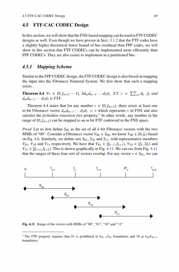
4.5 FTF-CAC CODEC Design 65
4.5 FTF-CAC CODEC Design
In this section, we will show that the FNS-based mapping can be used in FTF CODECdesigns as well. Even though we have proven in Sect. 3.1.2 that the FTF codes havea slightly higher theoretical lower bound of bus overhead than FPF codes, we willshow in this section that FTF CODECs can be implemented more efficiently thanFPF CODECs. They are also easier to implement in a partitioned bus.
4.5.1 Mapping Scheme
Similar to the FPF CODEC design, the FTF CODEC design is also based on mappingthe input into the Fibonacci Numeral System. We first show that such a mappingexists.
Theorem 4.4 ∀v ∈ [0, fm+2 − 1], ∃dmdm−1 · · · d2d1, S.T. v = ∑mk=1 dk · fk and
dmdm−1 · · · d2d1 is FTF.
Theorem 4.4 states that for any number v ∈ [0, fm+2), there exists at least onem-bit Fibonacci vector dmdm−1 · · · d2d1 = v which represents v in FNS and alsosatisfies the forbidden transition free property.1 In other words, any number in therange of [0, fm+2) can be mapped to an m bit FTF codeword in the FNS space.
Proof Let us first define S00 as the set of all k-bit Fibonacci vectors with the twoMSBs of “00”. Consider a Fibonacci vector V00 ∈ S00, we know V00 ∈ [0, fk) basedon Eq. 4.6. Similarly, we define sets S01, S10 and S11, with representative membersV01, V10 and V11 respectively. We have that V01 ∈ [fk−1, fk+1), V10 ∈ [fk , 2fk) andV11 ∈ [fk+1, fk+2). This is shown graphically in Fig. 4.11. We can see from Fig. 4.11that the ranges of these four sets of vectors overlap. For any vector v ∈ S01, we can
0 fk
fk+2
fk+1
2fk
fk-1
S00
S01
S10
S11
Fig. 4.11 Range of the vectors with MSBs of “00”, “01”, “10” and “11”
1 The FTF property requires that 01 is prohibited at b2k−1b2k boundaries and 10 at b2kb2k+1boundaries.

66 4 CODEC Designs for Memoryless Crosstalk Avoidance Codes
find an equivalent vector in S00 or S10. Similarly, any vector v ∈ S10 can be replacedby an equivalent vector in S01 or S11.
Now for a given number v, we can find an m bit vector Vin = dmdm−1 · · · d2d1 inthe FNS which represents v (based on the completeness of FNS). Now assuming that“01” is the prohibited pattern at the dkdk−1 boundary, we can replace dkdk−1 · · · d1with an equivalent k-bit vector in V00 or V10 to produce a new m bit vector Veq whichis equivalent to Vin. Note that Veq has no prohibited pattern at dkdk−1 boundary.
Also since “01” is the prohibited pattern at dkdk−1, the prohibited pattern atboundaries dk+1dk and dk−1dk−2 is “10”. We know that
• If Vin does not have the prohibited pattern at dk+1dk , then Veq does not introducethe prohibited pattern at dk+1dk , since the above manipulation causes the kth bitvalue to either change from ’0’ to ’1’ or no change at all.
• Veq does not have the prohibited pattern at dk−1dk−2 since dk−1 in Veq is ’0’.
The first condition guarantees that the manipulation do not introduce a prohib-ited pattern into more significant boundaries. The second condition guarantees thatthe manipulation does not introduce prohibited patterns in the next less significantboundary.
Therefore, by replacing the prohibited pattern iteratively from the MSB to theLSB, the final result is a vector which is equivalent to Vin, and is prohibited patternfree (and therefore it is a FTF codeword). This proves Theorem 4.4.
4.5.2 Coding Algorithm
To design a coding algorithm that maps each input value to an FTF codeword in theFNS, we observe that in Fig. 4.11, if dk is coded as
dk ={
0 if v < fk ,1 otherwise
(4.12)
and dk−1 is coded as
dk−1 ={
0 if v < fk+1,1 otherwise
(4.13)
then “01” is eliminated on dkdk−1. Conversely, if dk , is coded as
dk ={
0 if v < fk+1,1 otherwise
and dk−1 coded as
dk−1 ={
0 if v < fk−1,1 otherwise
then “10” is eliminated on dkdk−1.

4.5 FTF-CAC CODEC Design 67
Based on the above observations, the coding algorithm is shown in Algorithm 4.2.The algorithm generates FTF codewords with “01” prohibited at d2k+1d2k and “10”prohibited at d2kd2k−1.
Algorithm 4.2 FTF encoding algorithm: FTF-CAC(v)rm+1 = v;for k =m downto 2 do
if rk+1 < f2� k2 �+1 then
dk = 0;else
dk = 1;end ifrk = rk+1 − fk · dk ;
end ford1 = r2;Return: dmdm−1 · · · d1;
�·�: floor operator.
The encoding is carried out sequentially in m − 1 stages, similar to a divisionoperation. Starting from the MSB, each stage compares the input to a Fibonaccinumber and produces a coded bit as well as a remainder. The remainder from onestage becomes the input to the next stage.
4.5.3 Implementation and Experimental Results
A direct implementation of the encoder and decoder based on Algorithm 4.2 is illus-trated in Fig. 4.12 (here we assume m is even). The encoder, which converts a n-bitbinary vector v = bn · · · b1 to an m-bit Fibonacci vector V = dmdm−1···d1 , consists ofm − 1 stages. The decoder converts the codewords back to the original n-bit binaryvector.
The decoder in Fig. 4.12 is exactly the same as the decoder for FPF code shownin Fig. 4.12. It consists of an m input adder. The m inputs of the adder have differentnumbers of bits with the most significant input having the most number of bits(�log (fm)�) and two least significant inputs having 1 bit each. The m input adder is aspecial case of an arithmetic sum of product block, and can be synthesized efficiently[33]. The overall complexity is approximately O(m2/2).
dk ={
0 if rk+1 < f2� k2 �+1,
1 otherwise(4.14)
rk = rk+1 − fk · dk (4.15)
The encoder stages implement the arithmetic function given in Eq. 4.15. Each stageproduces a single bit dk and a remainder rk . For the MSB stage, the input rk+1 is the

68 4 CODEC Designs for Memoryless Crosstalk Avoidance Codes
<fm
<fm
dmrm
dm-1rm-1
<fm-2dm-2rm-2
<f4d3r3
<f2d2d1
dm-1
dm
fm
fm-1
d3
d2
d1
f3
v
v
encoder decoder
Fig. 4.12 FTF encoder and decoder block diagram
input data (v) to be encoded. For other stages, rk+1 is the remainder of the precedingstage. If m is even, the implementation requires one comparator, one adder and one2:1 MUX. If m is odd, the implementation only needs one adder and one MUXsince the adder (subtraction) also functions as a comparator. Assuming the hardwareresources required for a comparator are the same as for an adder, the total resourcesrequired for an m bit bus encoder is 3
2 m adders and m MUXes. The number of bitsreduces monotonically from the MSB stage to the LSB stage.
If we combine every two stages in the encoder carefully, the logic can be furthersimplified. Let “10” be the prohibited pattern for dkdk−1 boundaries. A two-bitencoder stage implements the following:
dkdk−1 =⎧⎨
⎩
00 if rk+1 < fk ,01 if rk+1 < fk+1,11 otherwise
rk−1 =⎧⎨
⎩
rk+1 if rk+1 < fk ,rk+1 − fk if rk+1 < fk+1,rk+1 − fk+1 otherwise
(4.16)
Equation 4.16 can be implemented using two adders and two MUXes. Since thesingle-bit stage implementation requires the resources for three adders and twoMUXes to encode two bits, the two-bit stage implementation of Eq. 4.16 is sim-pler. We should point out that this simplification is only achieved when “10” is theprohibited pattern. We can not reduce the implementation complexity if “01” is the
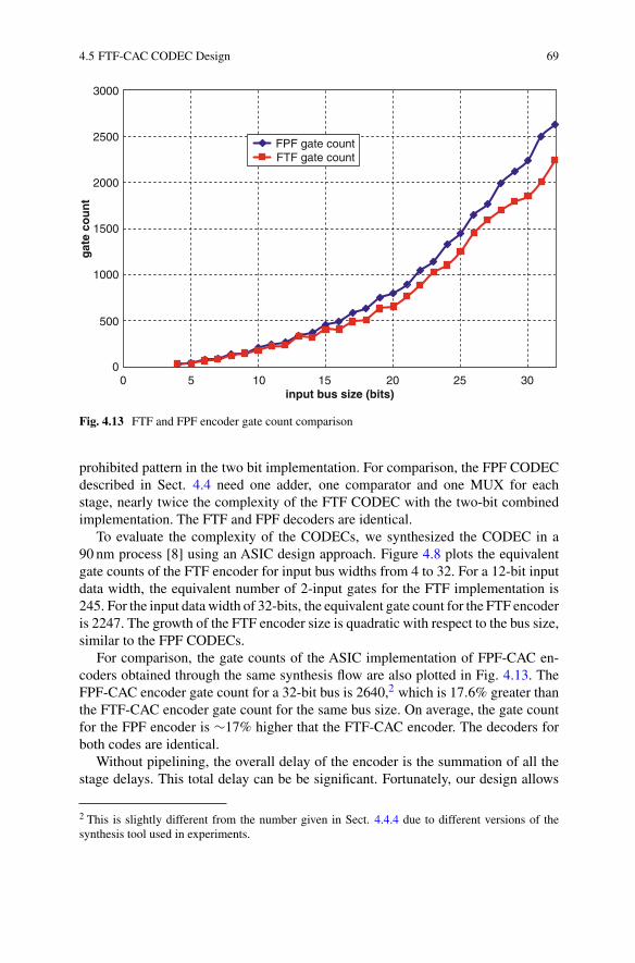
4.5 FTF-CAC CODEC Design 69
3000
FPF gate countFTF gate count
2500
2000
1500
1000
500
00 5 10 15
input bus size (bits)
gat
e co
un
t
20 25 30
Fig. 4.13 FTF and FPF encoder gate count comparison
prohibited pattern in the two bit implementation. For comparison, the FPF CODECdescribed in Sect. 4.4 need one adder, one comparator and one MUX for eachstage, nearly twice the complexity of the FTF CODEC with the two-bit combinedimplementation. The FTF and FPF decoders are identical.
To evaluate the complexity of the CODECs, we synthesized the CODEC in a90 nm process [8] using an ASIC design approach. Figure 4.8 plots the equivalentgate counts of the FTF encoder for input bus widths from 4 to 32. For a 12-bit inputdata width, the equivalent number of 2-input gates for the FTF implementation is245. For the input data width of 32-bits, the equivalent gate count for the FTF encoderis 2247. The growth of the FTF encoder size is quadratic with respect to the bus size,similar to the FPF CODECs.
For comparison, the gate counts of the ASIC implementation of FPF-CAC en-coders obtained through the same synthesis flow are also plotted in Fig. 4.13. TheFPF-CAC encoder gate count for a 32-bit bus is 2640,2 which is 17.6% greater thanthe FTF-CAC encoder gate count for the same bus size. On average, the gate countfor the FPF encoder is ∼17% higher that the FTF-CAC encoder. The decoders forboth codes are identical.
Without pipelining, the overall delay of the encoder is the summation of all thestage delays. This total delay can be be significant. Fortunately, our design allows
2 This is slightly different from the number given in Sect. 4.4.4 due to different versions of thesynthesis tool used in experiments.

70 4 CODEC Designs for Memoryless Crosstalk Avoidance Codes
FTF-ENCA
bn
bn/2+1
da m
da1
FTF-DECA
bn
bn/2+1
FTF-ENCB
bn/2
b1
dbm
db1
FTF-DECB
bn/2
b1
Fig. 4.14 FTF CODECs combined with bus partitioning
pipeline stages to be inserted between stages. The speed of the encoder is determinedby the slowest stage (the MSB stage). It is reported in [17] that a 64-bit adder hasa total delay of less than 250 ps using a 65 nm process. With the additional delay ofthe MUX, we estimate that the slowest stage of our CODEC (the MSB stage) has adelay of no more than 300 ps. Therefore, we expect a pipelined implementation ofthe FTF CODEC to operate at 3 GHz. It is important to note that pipelining cannotbe used in an encoder implemented as a flat design.
Again, the complexity and speed of the FTF CODEC can be further improved byapplying bus partitioning. The maximum input-to-output delay of the non-pipelinedm-bit encoder is τ (m) ∝ O(m2). The total area also exhibit a quadratic growth withthe number of input bits. Therefore partitioning the bus will reduce the total areaby ∼50%. Unlike FPF CODECs, which require either two shield wires between thegroup boundaries or more complicated techniques such as group complement forbus partitioning, the FTF code only needs one grounded wire between two adjacentgroups (as shown in Fig. 4.14). Therefore, the slight bus area overhead advantage ofFPF no longer exists when bus partitioning is applied.
4.6 Summary
This chapter covers CODEC designs for memoryless CACs. In particular, the dis-cussion was restricted to 3C-free codes. We confirmed that a flat implementationof a random or FNS-based mapping is impractical for large busses because of theexponential growth of CODEC size and the rapid speed degradation associated withthe size growth.
A challenging task in CAC code design is to find an efficient mapping. A quickanalysis shows that even a simple 4 ⇒ 5-bit CODEC will have over 2 ·1013 possiblemappings, hence exhaustive search is impossible.
To address this, we presented several solutions. We first presented two bus parti-tioning techniques, “group complement” in Sect. 4.2 and “bit-overlapping” in Sect.4.3. By partitioning the bus, the encoders and decoders are guaranteed to have limitedcomplexity, even if the mapping used are suboptimal, the associated penalty is accept-able due to the reduced size of the bus. Due to the lack of an optimal mapping scheme,

4.6 Summary 71
we implemented partitioned CODECs by using an arbitrary mapping. The undesiredcrosstalk patterns across the group boundaries are dealt with by complementing thegroup outputs or overlapping input bits. Even though the CODEC sizes are small,both schemes incur an extra area overhead and therefore are not deemed efficient.
We then presented solutions to the mapping which use the Fibonacci numeral sys-tem (FNS). Using the FNS based mapping solutions, we developed several CODECsfor both FPF and FTF 3C-free codes in Sect. 4.4 and 4.5 respectively.
For FPF codes, we first presented the mathematical proof that any number v has atleast one corresponding FPF vector in the FNS. Based on this mapping, we developedan encoding algorithm that produces FPF codes with near-optimal cardinality (i.e.,the coding scheme yields an area overhead which is at worst one bit greater than thetheoretical lower bound). We then presented an improved FPF coding scheme, whichachieves the theoretical bound in overhead efficiency. We showed that the optimalFPF encoding also follows the FNS mapping.
We also discussed FPF CODEC implementations. Encoders of both FPF CODECscan be implemented in multi-stage structure. Further optimizations were proposedto eliminate the MSB stage in the encoder, thereby simplifying the decoder as well.We implemented the near-optimal FPF CODEC in both an FPGA as well as a 90 nmASIC flow. The reported results show a quadratic growth in both CODEC size anddelay, with the increasing bus size. Our FNS-based CODECs are all several orders ofmagnitude smaller than a previously reported flat random mapping based CODEC[89]. The equivalent 2-input gate count for our FPF encoder is about 4,000 for a 32-bitbus. We also presented techniques to combine our approach with bus partitioning toaddress the propagation delay issue as well as to reduce the total size of the CODEC.
We also compared the average bus energy consumption of uncoded and FPF codedbusses, through simulation. Our experimental results show that FPF coding offerson average ∼20% energy saving.
We also presented FNS-based FTF CODEC designs. The existence of an FTFmapping in FNS for any number was first proven mathematically. We showed thatFNS-based FTF encoding algorithms are very efficient in terms of area overhead.We showed that the main advantage of FTF CODEC designs lie in their efficientimplementations. FTF encoders can be implemented in multi-stage structures, verysimilar to FPF encoders. However, each stage in an FTF encoder is simpler than thecorresponding stage of the FPF encoder in implementation. By combining two stages,the overall complexity of an FTF encoder is further reduced, requiring about half thenumber of arithmetic operations compared to the FPF encoder of the same bus size.Our ASIC-based implementation of the FTF encoders showed over 17% gate countreduction and nearly 50% speed improvement over FPF encoders implemented inthe same technology with the same design tools. Another benefit offered by the FTFencoder is that it yields more efficient partitioned implementation compared to theFPF encoder.
All the CODEC designs based on FNS mapping have the following features:
• Efficiency: Both the encoder and decoder complexities grow quadratically (asopposed to exponentially) with increasing bus size.

72 4 CODEC Designs for Memoryless Crosstalk Avoidance Codes
• Modularity: Both the encoder and decoder are constructed in a systematic fashion.The encoder consists of multiple stages, and a CODEC design for a larger buscan be generated from a CODEC of a smaller bus.
• Simplicity: Bus partitioning is elegantly handled.• Speed: The multi-stage implementation of FNS-based encoders enables easy
pipelining and extreme high-speed operation. In a non-pipelined implementa-tion, these encoders encounter a ripple delay effect and are slow for large bussizes.

Chapter 5Memory-based Crosstalk Avoidance Codes
Codewords generated in memory-based crosstalk avoidance encoding satisfy a spec-ified crosstalk upper-bound requirement with respect to the previous codeword onthe bus. The codeword is generated based not only on the current data word, but alsoon the previously transmitted codeword. Such a code is therefore called “memory-based code”. The decoder also uses the current received codeword and either theprevious received codeword or the previous decoded data word to decode the currentdata word. The memory depth of CACs we consider is one.
Memoryless crosstalk avoidance codes are attractive due to the simplicity of theirCODEC implementations. Memory-based codes, on the other hand, offer the ad-vantage of lower bus area overhead as reported in [35, 99]. However, they generallyrequire more complex CODECs.
In this chapter, we first present a memory-based 4C-free CAC design that requiressimple CODEC logic and 33% bus wiring overhead. We then present two genericmemory-based code design methods: the pruning-based search and the ROBDD-based search.
5.1 A 4C-Free CAC
The proposed 4C-free CAC eliminates all 4C crosstalk patterns on the bus and there-fore the bus satisfies maxj(Ceff , j) = (1 + 3λ)CL . For DSM processes, the speed isimproved by ∼33% since λ � 1. According to Table 2.4, for a 20 mm bus with 60×drivers, the signal delay is reduced from over 1500 to 1068 ps, and consequently a27% improvement is achieved in practice. (Note that this value may vary slightlyfor different driver sizes or bus lengths). These codes are less aggressive in reducingcrosstalk compared to other CACs discussed in previous chapters. However, theyincur a lower area overhead penalty, and therefore can be attractive in designs wherearea constraints are stringent.
5.1.1 A 4C-free Encoding Technique
To encode input data into 4C-free codewords, we split the input bus into groups of3-bits. These group signals are referred to as group data signals. For each group, we
C. Duan et al., On and Off-Chip Crosstalk Avoidance in VLSI Design, 73DOI 10.1007/978-1-4419-0947-3_5, © Springer Science+Business Media LLC 2010

74 5 Memory-based Crosstalk Avoidance Codes
add an additional signal called group complement indicator. When a group comple-ment indicator toggles, the bus receiver complements all the group data signals inthat group.
Let Vk be the input vector in the kth cycle. For the kth cycle, we denote the groupdata signals of group i as dk
i,j (for j = 1, 2, 3) and the group complement indicator of
group i as cki .
For two consecutive vectors Vk and Vk+1, let dki,1 = v1, dk
i,2 = v2, dki,3 = v3 and
cki = v4. Also, let dk+1
i,1 = v5, dk+1i,2 = v6, dk+1
i,3 = v7 and ck+1i = v8. We denote the
group transition as (v1, v2, v3, v4)ki → (v5, v6, v7, v8)k+1
i . If we refer only to the groupdata signals of group i, their transition is denoted as (v1, v2, v3)k
i → (v5, v6, v7)k+1i .
Whenever a 4C transition is detected on the group data signals, i.e., v1 = v5,v2 = v6, v3 = v7 and v1 = v3 = v2 the group data is transmitted as(v1, v2, v3, v4)k
i → (v1, v2, v3, v4)k+1i . The receiver complements the group data
signals accordingly (since the group complement indicator performs a transition)and correct data is recovered.
5.1.2 An Example
Consider two successive vectors (in the kth and k+1th cycles) on a 9-bit uncodedbus
(010 101 010)k → (101 010 101)k+1.
Spaces are provided to indicate group partitions. Note that 4C transitions occurs inall the groups. Now assume the bus is encoded using the scheme given above, andalso assume that the initial values of group complement indicators are 0 in the kthcycle. The transmitted 12-bit vector sequence becomes
(0100 1010 0100)k → (0101 1011 0101)k+1.
Note that in the transmitted vector above, none of the group data signals perform atransition. In this fashion, 4C transitions never occur within a group.
On further reflection, we realize that forbidden transitions can occur across groupsif this scheme is utilized. Consider a 6-bit bus and assume that the initial values ofall group complement indicators are 0. The un-encoded bus transitions are
(010 101)k → (101 011)k+1.
After encoding, the transmitted vector would be
(0100 1010)k → (0101 0110)k+1.
Note that in this case, a 4C transition occurs across the two groups (at the underlinedbit positions).

5.2 Codeword Generation by Pruning 75
We observe that such a 4C transition can only occur when the group complementindicator transitions. More precisely, it occurs when the group complement indicatorof group i performs a 0 → 1 (or 1 → 0) transition and the data signals of thegroup i + 1 perform a (10v)k
i+1 → (01v)k+1i+1 (or (01v)k
i+1 → (10v)k+1i+1 ) transition,
where v ∈ {0, 1}. Therefore this condition can be avoided by modifying the originalencoding scheme in the following manner:
Whenever 0 (or 1) = cki �= ck+1
i , and the group data signals of group i + 1 areof the form (10v)k
i+1 → (01v)k+1i+1 (or (01v)k
i+1 → (10v)k+1i+1 ) where v ∈ {0, 1}, we
complement ck+1i+1 and the group data signals of group i + 1 .
This complicates the bus encoding, possibly forces a rippling of data in the groupcomplement logic and results in a slower encoder.
Since every group of 3 input wires requires an additional wire, the area overheadof this coding scheme is
OH4C = 33%. (5.1)
5.2 Codeword Generation by Pruning
Graph theory based techniques can be very useful in analyzing situations involvinga set of elements in which various pairs of elements are related by certain proper-ties [19, 95]. In the case of crosstalk-based bus encoding, a graph GkC
m = (V , E)can be constructed for an m-bit bus.1 GkC
m consists of a set of 2m vertices, Vand a set of edges, E. Each v ∈ V represents one of 2m codewords that may betransmitted on the bus. An edge between two vertices a and b (denoted as (a, b)) in-dicates that transition between these two codewords satisfies the crosstalk constraint,i.e., max(Ceff , j) ≤ kC for the transition between a and b. The properties of GkC
minclude
1. |GkCm | = 2m, where |GkC
m | is the order of the graph.2. GkC
m is undirected2.3. For any v ∈ V , (v, v) ∈ E
Figure 5.1 illustrates the graphs for a 3-bit bus under different crosstalk constraints.The degree of a vertex, a, in GkC
m , denoted as dG(a), is the number of edges incidentwith the vertex. It represents the number of legal transitions from the current busvector, a. dG(a), and therefore, is the number of distinct data words that can betransmitted on the bus.
GkCm can be thought of as representing an m-bit bus. Any value can be present on
the bus and therefore the number of data words that can be encoded on to this m-bit
1 To simplify the notation, we sometimes use “kC” in place of “kC-free”. A kC bus is (k + 1)C-freeand therefore kC ≡ (k + 1)C-free.2 An edge is undirected if the initial vertex and the terminal vertex are not differentiated, i.e.,(a, b) ≡ (b, a). This property is warranted by the symmetry of bus crosstalk, i.e., X(a, b) ≡ X(b, a).

76 5 Memory-based Crosstalk Avoidance Codes
Fig. 5.1 Graphs for 3-bit busses under different crosstalk constraints a G3 graph b G4C−free3 graph
c G3C−free3 graph d G2C−free
3 graph e G1C−free3 graph
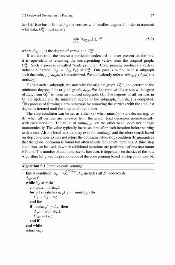
5.2 Codeword Generation by Pruning 77
(k+1)C-free bus is limited by the vertices with smallest degree. In order to transmitn-bit data, GkC
m must satisfy
mina∈V
[dGkCm (a)] ≥ 2n. (5.2)
where dGkCm (a) is the degree of vertex a in GkC
m .If we constrain the bus so a particular codeword is never present on the bus,
it is equivalent to removing the corresponding vertex from the original graph,GkC
m . Such a process is called “code pruning”. Code pruning produces a vertex-induced subgraph, Gp = (Vp, Ep) of GkC
m . Our goal is to find such a subgraphsuch that mina∈Vp (dGp(a)) is maximized. We equivalently refer to mina∈Vp (dG(a)) asmin(dGp ).
To find such a subgraph, we start with the original graph, GkCm , and determine the
minimum degree of the original graph, dmin. We then remove all vertices with degreeof dmin from GkC
m to form an induced subgraph, Gp. The degrees of all vertices inGp are updated and the minimum degree of the subgraph, min(dGp) is computed.This process of forming a new subgraph by removing the vertices with the smallestdegree is iterated until the stop condition is met.
The stop condition can be set as either (a) when min(dGp) start decreasing, or(b) when all vertices are removed from the graph. |Gp| decreases monotonicallywith each iteration. The value of min(dGp), on the other hand, does not changemonotonically. The value typically increases first after each iteration before startingto decrease. Also, a local maxima may exist for min(dGp) and therefore search basedon stop condition (a) may not return the optimum value. stop condition (b) guaranteesthat the global optimum is found but often results redundant iterations. A third stopcondition can be used, in which additional iterations are performed after a maximumis found. The number of additional steps, however, is dependent on the size of the bus.Algorithm 5.1 gives the pseudo-code of the code pruning based on stop condition (b).
Algorithm 5.1 Iterative code pruning
Initial condition: Gp = GkC−freem , Vp includes all 2m codewords;
dopt = 0;while Vp �= ∅ do
compute min(dGp);for all vi satisfies dGp(vi) = min(dGp) do
Gp = Gp − vi;end forif min(dGp) ≥ dopt then
dopt = min(dGp);Gopt = Gp;
end ifend whilereturn Gopt ;
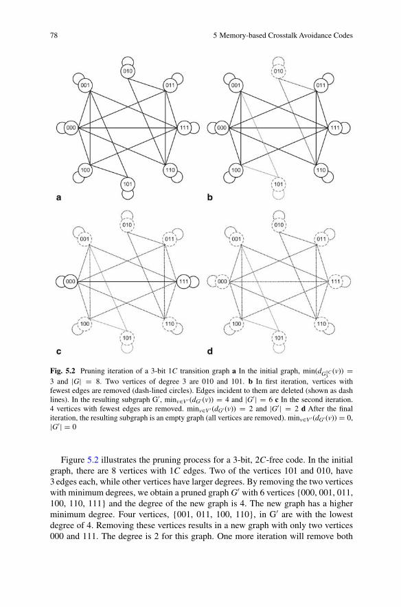
78 5 Memory-based Crosstalk Avoidance Codes
Fig. 5.2 Pruning iteration of a 3-bit 1C transition graph a In the initial graph, min(dG1C3
(v)) =3 and |G| = 8. Two vertices of degree 3 are 010 and 101. b In first iteration, vertices withfewest edges are removed (dash-lined circles). Edges incident to them are deleted (shown as dashlines). In the resulting subgraph G′, minv∈V ′ (dG′ (v)) = 4 and |G′| = 6 c In the second iteration.4 vertices with fewest edges are removed. minv∈V ′ (dG′ (v)) = 2 and |G′| = 2 d After the finaliteration, the resulting subgraph is an empty graph (all vertices are removed). minv∈V ′ (dG′ (v)) = 0,|G′| = 0
Figure 5.2 illustrates the pruning process for a 3-bit, 2C-free code. In the initialgraph, there are 8 vertices with 1C edges. Two of the vertices 101 and 010, have3 edges each, while other vertices have larger degrees. By removing the two verticeswith minimum degrees, we obtain a pruned graph G′ with 6 vertices {000, 001, 011,100, 110, 111} and the degree of the new graph is 4. The new graph has a higherminimum degree. Four vertices, {001, 011, 100, 110}, in G′ are with the lowestdegree of 4. Removing these vertices results in a new graph with only two vertices000 and 111. The degree is 2 for this graph. One more iteration will remove both
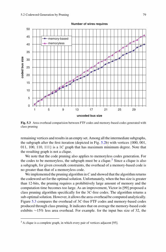
5.2 Codeword Generation by Pruning 79
Number of wires requires
memory-based
memoryless
50
45
40
35
30
25
20
15
10
5
01 5 9 13 17 21 25 29
uncoded bus size
cod
ed b
us
size
Fig. 5.3 Area overhead comparision between FTF codes and memory-based codes generated withclass pruning
remaining vertices and results in an empty set. Among all the intermediate subgraphs,the subgraph after the first iteration (depicted in Fig. 5.2b) with vertices {000, 001,011, 100, 110, 111} is a 1C graph that has maximum minimum degree. Note thatthe resulting graph is not a clique.
We note that the code pruning also applies to memoryless codes generation. Forthe codes to be memoryless, the subgraph must be a clique.3 Since a clique is alsoa subgraph, for given crosstalk constraints, the overhead of a memory-based code isno greater than that of a memoryless code.
We implemented the pruning algorithm in C and showed that the algorithm returnsthe codeword set for the optimal solution. Unfortunately, when the bus size is greaterthan 12-bits, the pruning requires a prohibitively large amount of memory and thecomputation time becomes too large. As an improvement, Victor in [99] proposed aclass pruning algorithm specifically for the 3C-free codes. The algorithm returns asub-optimal solution. However, it allows the area-overhead be computed analytically.Figure 5.3 compares the overhead of 3C-free FTF codes and memory-based codesproduced through class pruning. It indicates that on average the memory-based codeexhibits ∼15% less area overhead. For example. for the input bus size of 32, the
3 A clique is a complete graph, in which every pair of vertices adjacent [95].

80 5 Memory-based Crosstalk Avoidance Codes
memory-based code requires only 40 wires, as opposed to 46 wires needed for amemoryless code.
5.3 Codeword Generation Using ROBDD
In this section, we present a method for memory-based code generation using Re-duced Ordered Binary Decision Diagrams (ROBDDs) [22]. It is a two-step approachto determine the effective bus of width n that can be encoded in a kC-free manner,(for 1 ≤ k ≤ 4) using a physical bus of width m:
• First, we construct an ROBDD GkC−freem which encodes all vector transitions on
the m-bit bus that are kC free.• From GkC−free
m , we find the effective bus width n, such that an n-bit data bus canbe encoded in a kC free manner using GkC−free
m .
5.3.1 Efficient Construction of GkC−freem
In the first step, we employ an ROBDD-based construction of GkC−freem . In particular,
we inductively compute GkC−freem . Since the ROBDD of a logic function and its
complement contain the same number of nodes (except for a complement pointer),this enables an efficient construction of GkC−free
m . Further, the ROBDD allows us torepresent the legal (and illegal) kC free crosstalk transitions on the bus implicitly,share nodes maximally and in a canonical manner.
Suppose we want to construct GkC−freem . In this case, we allocate 2m ROBDD
variables. The first m variables correspond to the vector from which a transition ismade (referred to as v = {v1, v2, · · · , vm}). The next m variables correspond to thevector to which a transition is made (referred to as w = {w1, w2, · · · , wm}). If avector sequence v∗ → w∗ is legal with respect to kC crosstalk, then w∗ → v∗ is alsolegal. In other words, GkC−free
m (v∗, w∗) = GkC−freem (w∗, v∗).
We construct the ROBDD for GkC−freem by using ROBDDs of intermediate, par-
tially kC cross-talk free ROBDDs GkCi (3 ≤ i ≤ m). The construction of the ROBDD
of GkCm proceeds inductively, starting with the base case of GkC
3 . The construction ofG4C
3 , G3C3 and G2C
3 are described next.
G4C3 =
⎡
⎢⎢⎢⎣
v︷ ︸︸ ︷v1 v2 v3 v4 · · · vm
1 0 1 − · · · −0 1 0 − · · · −
w︷ ︸︸ ︷w1 w2 w3 w4 · · · wm
0 1 0 − · · · −1 0 1 − · · · −
⎤
⎥⎥⎥⎦
We initialize G3C3 with the transitions of G4C
3 , and then append additional 3 · Ctransitions:
G3C3 = G4C
3

5.3 Codeword Generation Using ROBDD 81
G3C3 + =
⎡
⎢⎢⎢⎢⎢⎢⎢⎢⎢⎢⎢⎢⎢⎢⎢⎢⎣
v︷ ︸︸ ︷v1 v2 v3 v4 · · · vm
0 0 1 − · · · −0 1 0 − · · · −1 0 1 − · · · −1 1 0 − · · · −0 1 0 − · · · −1 0 0 − · · · −0 1 1 − · · · −1 0 1 − · · · −
w︷ ︸︸ ︷w1 w2 w3 w4 · · · wm
0 1 0 − · · · −0 0 1 − · · · −1 1 0 − · · · −1 0 1 − · · · −1 0 0 − · · · −0 1 0 − · · · −1 0 1 − · · · −0 1 1 − · · · −
⎤
⎥⎥⎥⎥⎥⎥⎥⎥⎥⎥⎥⎥⎥⎥⎥⎥⎦
Similarly, we initialize G2C3 with the transitions of G3C
3 , and then append additional2C transitions:
G2C3 = G3C
3
G2C3 + =
⎡
⎢⎢⎢⎢⎢⎢⎢⎢⎢⎢⎢⎢⎢⎢⎢⎢⎢⎢⎢⎢⎢⎢⎢⎢⎢⎢⎢⎢⎢⎢⎢⎢⎢⎢⎢⎢⎢⎢⎢⎢⎢⎢⎢⎣
v︷ ︸︸ ︷v1 v2 v3 v4 · · · vm
0 0 1 − · · · −1 1 0 − · · · −1 0 0 − · · · −0 1 1 − · · · −0 1 0 − · · · −0 0 0 − · · · −1 1 1 − · · · −1 0 1 − · · · −0 0 1 − · · · −0 1 1 − · · · −1 0 0 − · · · −1 1 0 − · · · −0 1 0 − · · · −0 0 0 − · · · −1 0 1 − · · · −1 1 1 − · · · −0 0 1 − · · · −1 0 0 − · · · −0 1 1 − · · · −1 1 0 − · · · −
w︷ ︸︸ ︷w1 w2 w3 w4 · · · wm
1 1 0 − · · · −0 0 1 − · · · −0 1 1 − · · · −1 0 0 − · · · −1 1 1 − · · · −1 0 1 − · · · −0 1 0 − · · · −0 0 0 − · · · −0 1 1 − · · · −0 0 1 − · · · −1 1 0 − · · · −1 0 0 − · · · −0 0 0 − · · · −0 1 0 − · · · −1 1 1 − · · · −1 0 1 − · · · −1 0 0 − · · · −0 0 1 − · · · −1 1 0 − · · · −0 1 1 − · · · −
⎤
⎥⎥⎥⎥⎥⎥⎥⎥⎥⎥⎥⎥⎥⎥⎥⎥⎥⎥⎥⎥⎥⎥⎥⎥⎥⎥⎥⎥⎥⎥⎥⎥⎥⎥⎥⎥⎥⎥⎥⎥⎥⎥⎥⎦
Note that the ROBDDs for G4C3 , G3C
3 and G2C3 are only partially free of 4C, 3C and
2C transitions. They are immune to 4C, 3C and 2C transitions only on the first three

82 5 Memory-based Crosstalk Avoidance Codes
bits of the bus. We utilize the complements of these ROBDDs to construct GkC−freem
(for k = 2, 3 and 4) . The ROBDD GkC−freem is free of kC transitions for all m-bits of
the bus.Algorithm 5.2 describes the inductive construction of GkC−free
m from GkC3 . In
this algorithm, GkC3 ((vi, vi+1, vi+3) ← (v1, v2, v3), (wi, wi+1, wi+3) ← (w1, w2, w3))
refers to the ROBDD variable substitution of (vi, vi+1, vi+3) and (wi, wi+1, wi+3) by(v1, v2, v3) and (w1, w2, w3) respectively.
Algorithm 5.2 Inductive Construction of GkC−freem from GkC
3
for i = 1 to m − 3 doGkC
i+3 = GkCi+2 + GkC
3 ((vi+1, vi+2, vi+3) ← (v1, v2, v3), (wi+1, wi+2, wi+3)← (w1, w2, w3))
end forGkC−free
m ← GkCm
return GkC−freem
Note that only the final GkC−freem that is constructed using Algorithm 5.2 is utilized
for CODEC construction, since the intermediate ROBDDs for GkCi (i < m) will
possibly have kC or greater crosstalk transitions, since they are expressed over 2mvariables.
5.3.2 An Example
As an example, let us construct a G4C−free5 . We start by constructing G4C
3 as discussedearlier:
G4C3 =
⎡
⎢⎢⎢⎣
v︷ ︸︸ ︷v1 v2 v3 v4 v5
1 0 1 − −0 1 0 − −
w︷ ︸︸ ︷w1 w2 w3 w4 w5
0 1 0 − −1 0 1 − −
⎤
⎥⎥⎥⎦
Next we run Algorithm 3.1. Two iterations of the for loop are required, and theirintermediate results are:
G4C4 =
⎡
⎢⎢⎢⎢⎢⎢⎢⎣
v︷ ︸︸ ︷v1 v2 v3 v4 v5
1 0 1 − −0 1 0 − −− 1 0 1 −− 0 1 0 −
w︷ ︸︸ ︷w1 w2 w3 w4 w5
0 1 0 − −1 0 1 − −− 0 1 0 −− 1 0 1 −
⎤
⎥⎥⎥⎥⎥⎥⎥⎦
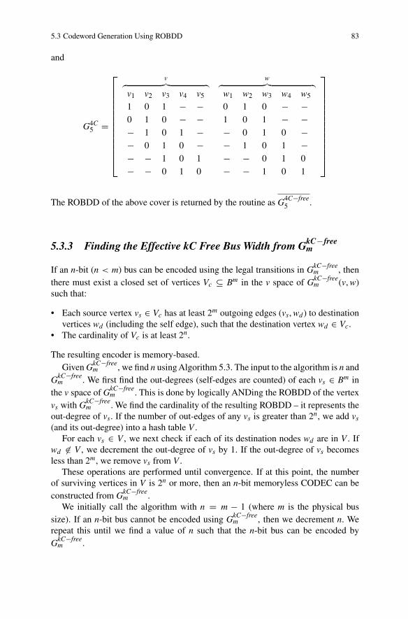
5.3 Codeword Generation Using ROBDD 83
and
G4C5 =
⎡
⎢⎢⎢⎢⎢⎢⎢⎢⎢⎢⎢⎢⎣
v︷ ︸︸ ︷v1 v2 v3 v4 v5
1 0 1 − −0 1 0 − −− 1 0 1 −− 0 1 0 −− − 1 0 1
− − 0 1 0
w︷ ︸︸ ︷w1 w2 w3 w4 w5
0 1 0 − −1 0 1 − −− 0 1 0 −− 1 0 1 −− − 0 1 0
− − 1 0 1
⎤
⎥⎥⎥⎥⎥⎥⎥⎥⎥⎥⎥⎥⎦
The ROBDD of the above cover is returned by the routine as G4C−free5 .
5.3.3 Finding the Effective kC Free Bus Width from GkC−freem
If an n-bit (n < m) bus can be encoded using the legal transitions in GkC−freem , then
there must exist a closed set of vertices Vc ⊆ Bm in the v space of GkC−freem (v, w)
such that:
• Each source vertex vs ∈ Vc has at least 2m outgoing edges (vs, wd) to destinationvertices wd (including the self edge), such that the destination vertex wd ∈ Vc.
• The cardinality of Vc is at least 2n.
The resulting encoder is memory-based.Given GkC−free
m , we find n using Algorithm 5.3. The input to the algorithm is n andGkC−free
m . We first find the out-degrees (self-edges are counted) of each vs ∈ Bm inthe v space of GkC−free
m . This is done by logically ANDing the ROBDD of the vertexvs with GkC−free
m . We find the cardinality of the resulting ROBDD – it represents theout-degree of vs. If the number of out-edges of any vs is greater than 2n, we add vs
(and its out-degree) into a hash table V .For each vs ∈ V , we next check if each of its destination nodes wd are in V . If
wd �∈ V , we decrement the out-degree of vs by 1. If the out-degree of vs becomesless than 2m, we remove vs from V .
These operations are performed until convergence. If at this point, the numberof surviving vertices in V is 2n or more, then an n-bit memoryless CODEC can beconstructed from GkC−free
m .We initially call the algorithm with n = m − 1 (where m is the physical bus
size). If an n-bit bus cannot be encoded using GkC−freem , then we decrement n. We
repeat this until we find a value of n such that the n-bit bus can be encoded byGkC−free
m .

84 5 Memory-based Crosstalk Avoidance Codes
Algorithm 5.3 Testing if GkC−freem can encode an n-bit bus
test_encoder(n, GkC−freen )
find out − degree(vs) of each node vs, insert (vs, out − degree(vs)) in V if out −degree(vs) ≥ 2n
degrees_changed = 1while degrees_changed do
degrees_changed = 0for each vs ∈ V do
for each wd S.T. GkC−freem (vs, wd) = 1 do
if wd �∈ V thendecrement out − degree(vs) in Vdegrees_changed = 1
end ifif out − degree(vs) < 2n then
V ← V \ vs
breakend if
end forend for
end whileif |V | ≥ 2n then
print(n-bit bus may be encoded using GkC−freem )
elseprint(n-bit bus cannot be encoded using GkC−free
m )end if
5.3.4 Experimental Results
We ran our algorithm to construct GkC−freem and to find the effective bus width n for
4C, 3C and 2C free transitions. The ROBDD of GkC−freem is constructed as described
in Sect. 5.3.1, and the test for the effective bus width is performed as described inSect. 5.3.3. Based on the values of m and the corresponding effective bus width n,we plot the overhead in Fig. 5.4.
Note that this figure indicates that the asymptotic bus size overheads for thememory based codes are much lower than the memoryless code overheads. Theoverhead for a 2C free memory based code is about 117% compared to 146% fora memoryless code. The overhead for a 3C free memory based code is about 30%compared to 44% for a memoryless code. The overhead for a 4C free memory basedcode is about 8% compared to 33% for a memoryless code.
The memory-based CODEC designs are more complicated. Bus partitioning canalso be used in the memory-based CODEC designs, where a wider bus, is partitionedinto small groups and encoded and decoded independently.

5.4 Summary 85
Fig. 5.4 Bus size over-heads for Memory-basedCODECs
160
140
120
100
80
60
40
20
04 5 6 7 8 9 10 11 12 13
Ove
rhea
d %
Real bus width
2C-free3C-free4C-free
The standard-cell based implementation of the encoder and decoder involves afew levels of logic, and its delay is estimated to be 250 ps. This delay can be reducedfurther by using Programmable Logic Arrays (PLAs) to implement the CODECcircuitry.
5.4 Summary
Memory-based CACs have been discussed in this chapter. Compared to memorylesscodes, memory-based CACs have lower area overhead and therefore can be attractive.The biggest disadvantage of the memory-based code is the high complexity of theirCODECs.
In Sect. 5.1, we presented a very simple 4C-free code design. It requires 33%overhead and the CODEC is very simple to implement. In Sects. 5.2 and 5.3, we dis-cussed two general design techniques for memory-based code design: code pruningand the ROBDD-based approach.
In the code pruning approach, we first represent the bus transitions using a graph.Code pruning is equivalent to finding a subgraph that maximizes the minimal degree.Even though code pruning is used for memory-based code design, it can also be usedfor memoryless code design by constraining the resulting subgraph to a clique.
Codeword pruning returns codewords with optimal overhead. However, the highmemory requirement and large run time of this approach make it impractical forlarge busses. Our experimental results show that memory-based 3C-free codes onaverage have a 15% lower overhead than their memoryless counterparts.
A second codeword searching algorithm we proposed is based on ROBDDs. In thisapproach, instead of explicitly enumerating all legal bus transitions, we enumerateonly the illegal transitions inductively, and then derive the ROBDD for the legaltransitions. The ROBDD-based approach represents the transitions in a compact and

86 5 Memory-based Crosstalk Avoidance Codes
canonical fashion. The algorithm to find the effective kC free bus bandwidth n of abus with physical width m was also presented.
Both approaches demonstrated that theoretically, the overheads can be as lowas 117%, 30% and 8% for memory-based CODECs that are free of 4C, 3C and2C transitions respectively, which is much lower than the area overheads for thecorresponding memoryless codes, which are 146%, 44% and 33% respectively.

Chapter 6Multi-Valued Logic Crosstalk Avoidance Codes
So far, the discussions on on-chip crosstalk avoidance have been limited to binaryvalued busses. This can be attributed to the fact that binary-valued busses are almostexclusively used for on-chip interconnects in today’s digital circuits thanks to theirseamless ability to interface with the logic circuit. Further, binary-valued bussesresult in simple driver and receiver designs, with low power consumption. However,multi-valued busses have their advantages over the binary busses. In this chapter,we shift the focus of the discussion to how to built crosstalk avoiding multi-valuedbusses. We will show that multi-valued busses can out perform binary-valued bussesin speed, power and area-overhead.
A multi-valued bus is a bus in which each digit can represent more than two logicvalues, as opposed to two values in a binary bus. Physically, these logic values arerepresented by different voltage levels or sometimes current levels. For illustrationpurposes, we will assume the voltage mode implementation unless otherwise spec-ified. Figure 6.1 shows the waveform of a 4-valued bus wire. To achieve maximumnoise margin, the circuit is implemented such that the voltage levels representingeach value are evenly separated between 0V and Vdd . Therefore, for N-valued logic,the voltage values are {0, 1
N−1 Vdd , 2N−1 Vdd · · · N−2
N−1 Vdd , Vdd} and the voltage step is
Vstep = 1N−1 Vdd .
Compared to a parallel binary-valued bus, the main advantage of a multi-valuedparallel bus is that each wire carries more information and therefore the bit densityis higher. The bit density of an N-valued logic signal is computed as ρ(N) = log2N .For the 4-valued logic bus, every wire represents 2 binary bits since ρ(4) = 2. For aternary (3-valued) bus, ρ(3) = 1.585 and for a decimal (10-level) bus, ρ(10) = 3.32.A higher bit density greatly reduces the number of wires needed for representingvalues in a given range. For bus interconnects, this often means fewer wires arerequired.
A widely used high-speed interconnect design technique is to reduce the signalswing. It improves signal speed since the delay is proportional to the voltage swing,and also reduces the power consumption. The related idea of multi-valued busseshas been studied for high throughput interconnect as it offers higher bit density thanbinary busses [18, 71, 98, 103]. The 4-level pulse amplitude modulation (PAM) is apopular multi-valued logic data transmission approach [18, 103]. It offers sufficient
C. Duan et al., On and Off-Chip Crosstalk Avoidance in VLSI Design, 87DOI 10.1007/978-1-4419-0947-3_6, © Springer Science+Business Media LLC 2010

88 6 Multi-Valued Logic Crosstalk Avoidance Codes
Fig. 6.1 Illustration of a 4-valued logic waveforms
noise margin and the number of logic levels is a power of two. However, crosstalkwas not addressed in any of these papers and all these research has been strictlylimited to off-chip interconnects.
6.1 Bus Classification in Multi-Valued Busses
In Chap. 2, we defined an effective capacitance for binary busses as
Ceff , j = CL · (1 + λ(2 − δj, j−1 − δj, j+1))
and showed that both the energy consumption and signal delay of a data line can beexpressed as functions of Ceff . For example, the delay on the jth line is given as
τj = k · abs(CL · �Vj + CI · �Vj, j−1 + CI · �Vj, j+1) (6.1)
where �Vj is the voltage change on the jth line and �Vj,k = �Vj −�Vk is the relativevoltage change between the jth and kth line. Assuming the output voltage levels areVdd and 0V, we have �Vj ∈ {0, ±Vdd} and �Vj,k ∈ {0, ±Vdd , ±2Vdd}.
If we let Vstep be the voltage step between logic levels (Vstep = Vdd for a binarybus). Equation 6.1 can be rewritten as
τj = k · CL · Vstep · abs(δj + 2λ · δj − λ · δj, j−1 − λ · δj, j+1). (6.2)
here δj = abs( �VjVstep
) is the normalized signal transition and δj,k = sign(Vj)·�VkVstep
isthe normalized relative transition. For an N-level bus, δj = {0, 1, · · · , N − 1} andδj,k = {0, ±1, · · · ± (N − 1)}. When N = 1, the bus is binary, and δj = 1 when thereis a transition on the jth line, otherwise δj = 0; δj,k = 1 when both jth and kth linestransition in the same direction, −1 when they transition in opposite directions and0 otherwise.
We define a normalized total crosstalk of the jth line (Xeff , j) as
Xeff , j = abs(2δj − δj, j−1 − δj, j+1), (6.3)

6.1 Bus Classification in Multi-Valued Busses 89
and for a N-valued bus, we know
min{Xeff , j} = 0
max{Xeff , j} = 4 · (N − 1).
The maximum Xeff , j occurs when δj = −δj, j−1 = −δj, j+1 = ±(N −1), i.e., the wirein the middle transitions from one extreme value to the other extreme value and thetwo adjacent wires transition from one extreme level to the other extreme level inthe opposite direction. For a binary bus, max{Xeff, j} = 4. The relation between Xeff , j
and Ceff , j can be expressed as
Ceff , j = (1 + λXeff , j)CL ≈ Xeff , j · CI .
min{Xeff , j} = 0 occurs when δj, j−1 = δj, j+1 = δj. max{Xeff , j} = 4 occurs whenδj, j−1 = δj, j+1 = −δj.
The signal delay on a multi-valued bus can be derived following the method givein Chap. 2. It is a function of Xeff , j expressed as follows:
τj = k · CL · Vstep · abs(δj + λ · Xeff , j) (6.4)
When λ � 1, Eq. 6.4 can be approximated as
τj = k · CL · Vstep · abs(λ · Xeff , j) (6.5)
Again, the delay τj is approximately linearly proportional to Xeff , j and the maximumbus speed is limited by the value of max{Xeff , j}. Based on the value of Xeff , j, wedefine the vector sequences on a N-level bus as 0X, 1X, 2X, . . . 4(N − 1)X sequencesand the bus can be classified as a 0X, 1X . . . 4(N − 1)X bus, determined by the valuesof maxj{Xeff , j}. A kX bus satisfies maxj{Xeff , j} ≤ k.
The energy consumption is also a function of Xeff , j and is given as
Ej = CL�Vj · Vdd − λCL(2�Vj − �Vj−1 − �Vj+1)Vdd
= CL · Vstep · Vdd · abs(δj + λ · Xeff , j)
= ELj + λEI
j (6.6)
Equation 6.6 again shows that the energy consumption for each bit is separated intotwo parts: EL
j is the energy to charge/discharge the load capacitance, and EIj the
energy to charge/discharge the capacitance to adjacent wires. Again, the first term isnegligible for DSM processes. The total energy consumption of the bus is given as
Etotal =n∑
j=1
ELj + λ
n∑
j=1
EIj
=n∑
j=1
(1 + Xeff , j · λ)CL · �V2j (6.7)
90 6 Multi-Valued Logic Crosstalk Avoidance Codes
6.2 Low Power and Crosstalk Avoiding Codingon a Ternary Bus
The above equations give the signal delay and power consumption for busses with anarbitrary number of levels, N . A large N , however, results in reduced noise margins.In today’s technology, the supply voltages have scaled down to 1V or lower. Toguarantee sufficient noise margins, N is generally limited to a small value in practice.In this section, we will discuss crosstalk avoidance in ternary busses. A voltage-modeternary bus has three output levels: Vdd , Vdd/2 and 0V and therefore the signal swingVstep = Vdd/2. δj, δj, j+1 and δj, j−1 vary within [−2, 2]. The maximum value of Xeff
can be as high as 8.Notation: In the following discussion, the three logic values on the ternary bus
are denoted in bold as +1, 0, −1, representing the high, middle and low valuesrespectively. For clarity, they are sometimes simplified as +, 0, −. Binary values aremarked with underlines. For example, 101 indicates a 3-bit binary value and +0+is a 3-bit ternary value. Also, ‘⇒’ denotes a mapping operation and ‘→’ indicates atransition.
6.2.1 Direct Binary-Ternary Mapping
As shown before, a ternary bus has a higher “bit density” if it is used to represent atrue ternary vector, as each ternary bit can represent 1.585 binary bits. Hence, an n-bitternary bus can be used to replace an m-bit binary bus if n ≥ �1/log23n� ≈ 0.63 m.However, the conversion between binary and ternary logic is complex and expensiveto implement in VLSI. Thus a true ternary bus is rarely used for interconnect. Instead,we propose a ternary bus interconnect for binary logic based on a direct bit-to-bitmapping scheme. The mapping between the binary logic and ternary-valued bus isas follows:
1. Each binary bit is mapped directly to a line on the ternary bus, hence n = m;2. A binary 0 is always mapped to a middle value on the ternary bus. i.e., 0⇒ 0;3. A binary 1 is mapped to either high or low value on the ternary bus. i.e. 1⇒ + or
1⇒ −.
Such a direct mapping scheme offers two advantages: it makes the encoding/decodinglogic simple, and it also offers flexibility on the polarity for the binary 1. For exam-ple, the ternary vectors +0+, −0−, +0− and −0+ all represent the same binaryvalue 101. Table 6.1 gives several examples of ternary transition sequences and thecorresponding Xeff on the middle bit. Notice that in this table, +0+→0+0 producesa 4X crosstalk (on the middle line). For +0+→0−0, Xeff = 0. In our mappingscheme, both these ternary sequences represent the same binary sequence 101→010. Similarly, the 000→0++ transition has much less crosstalk (1X) compared to000→0+−, which encodes the same binary sequence but produces 4X crosstalk. Inthe extreme case, +−+→+−+ is an 8X sequence but a +++→ −−− is a 0Xsequence, and both represent the same binary sequence.

6.2 Low Power and Crosstalk Avoiding Coding on a Ternary Bus 91
Table 6.1 Examples of total crosstalk in a ternary bus
Vt−1 Vt Xeff
000 +++ 0000 0++ 1000 0+− 3+0+ 0+0 4+0+ 0−0 0−+ 0 +−0 6+−+ −+− 8+++ −−− 0
If we define the bit polarity as the sign of the ternary representation for a binary‘1’, the above comments show that the bit polarity can affect crosstalk significantly.The following two coding schemes exploit the flexibility in our mapping scheme toreduce the crosstalk, thereby yielding energy savings and an increase in speed.
6.2.2 4X Ternary Code
We first show the construction of a ternary sequence that eliminates 5X and highercrosstalk. We call this a “4X ternary code” since it satisfies
max{Xeff, j} ≤ 4, ∀j ∈ [1, n]
Let bj be the jth bit of the input vector, Pj the polarity and Dj the magnitude of thecorresponding ternary representation. The following are the rules for constructingthe 4X ternary sequence:
1. On any bit, direct ‘+→−’ or ‘−→+’ transitions are prohibited.2. 1 → 0 is mapped as +→0 or −→0.3. For a 0→1 transition on bj, if bj−1 transitions, Pj is coded so both lines transition
in the same direction.4. For a 0→1 transition on bj, if bj−1 does not transition and bj+1 transitions from
1 to 0, Pj is coded so that the jth and the ( j + 1)th lines transition in the samedirection.
5. For a 0→1 transition on bj, if no transition occurs on either neighbor, Pj is codedso {Pj = Pj−1 or Pj = Pj+1} with Pj = Pj−1 having the higher priority.
The first rule guarantees a maximum of 4X crosstalk on any bit of the ternary bus.Compared to a ternary bus without crosstalk avoidance coding where max{Xeff, j} =8, our coding will boost the bus speed by approximately a factor of 2. The additionalrules allowing the encoder to choose the bit polarity to minimize local crosstalkwhenever it is possible. This results in total crosstalk reduction and therefore lowersthe bus power consumption. Table 6.3 gives an example of the output sequenceproduced of the 4X ternary code for a given binary sequence.

92 6 Multi-Valued Logic Crosstalk Avoidance Codes
Table 6.2 Ternary driver truth table
Magnitude Polarity Logic value VoltageDj Pj tj
0 X 0 V0
1 0 − V−1 1 + V+
Table 6.3 4X ternary sequence example
Binary Ternary Xeff
11110111 ++−000−+00110101 00−−0+0+ 0110012111100011 ++−000−+ 0122011101010100 0+0+0+00 1011212210101110 −0−0−+−0 0000102101110001 0+−+000− 0121220000000011 000000−− 1343112100011110 000+++−0 00110121
A CODEC can be easily implemented to satisfy all the rules above. As illustratedin Fig. 6.2, the inputs of the encoder are the binary vector b1b2 . . . bn and the outputis a ternary vector t1t2 . . . tn. Each line driver circuit can be considered of havingtwo parts, the polarity encoder and the ternary driver. The ternary driver outputs the3-level signal tj based on the polarity (Pj) and magnitude (Dj) using the truth tablegiven in Table 6.2. The jth polarity encoder has inputs of bj−1bjbj+1 and Pj−1PjPj+1.Since the encoders for all lines are identical except for the boundary bits b0 and bn,a very efficient implementations can be realized due to the regularity. Figure 6.2illustrates such an encoder.
Fig. 6.2 4X encoder anddriver circuit

6.2 Low Power and Crosstalk Avoiding Coding on a Ternary Bus 93
6.2.3 3X Ternary Code
The 4X-code lowers the probability of 4X crosstalk significantly as we can see fromTable 6.3. The maximum speed of a 4X-code bus is still limited by Xeff = 4. Tofurther improve the bus speed, we propose a modified coding scheme that eliminatesthe 4X crosstalk completely. The coding scheme is called “3X ternary code” as itsatisfies
max{Xeff , j} ≤ 3, ∀j ∈ [1, n]
The 3X code is constructed by partitioning the bus into 5-bit lanes (groups) andinserting a grounded wire between lanes as a shield. Now we apply the same 5 rulesgiven in Sect. 6.2.2. Compared to the 4X code, such a design will have up to 20%area overhead. Since the 3X code can speed up the bus by ∼33% compared to a 4Xbus, this coding scheme offers an additional 11% gain in the throughput per unit area.
The proof that such codec cancels all 4X and higher crosstalk is given as follows:
Proof
1. The prohibition of a direct +↔− transition eliminates all the crosstalk over 4Xsince the maximum crosstalk on each side of the jth wire cannot exceed 2X.
2. With the + ↔ − transition prohibited, there are 16 transitions that can produce4X crosstalk on the line in the middle. Each pair exhibits 2X crosstalk on eitherside. The full list is not given here to save space.
3. Due to the flexibility given to the polarity of a binary ‘1’, we can remove all butthe pairs with XXX→X00 patterns. There are four such pairs: +−+→000,−+−→000, 0−+→−00 and 0+−→+00. They can be generalized in two cases:ABA→000 and 0AB→A00, where A and B represent two values of oppositepolarities.
4. In the case of ABA→000, we can prove that it is possible to prevent ABA fromappearing on a bus that is no more than 5-bits wide. Considering a 3-bit slicetjtj+1tj+2 on the bus, since no direct transitions between A and B are allowed, theABA pattern can only be formed from patterns that contain at least one 0. Let thepolarity of tj+1 and tj+2 be selected based solely on its left neighboring bits. Ifeither tj+1 or tj+2 in the previous cycle has the value of 0, this rule guaranteesthat an ABA will not be formed. Therefore the only other scenario we need toexamine is the 0BA→XBA transition. If tj can be coded as either A or B, we canavoid ABA. This flexibility on tj can be guaranteed if the Xeff between tj−2 andtj−1 is no more than 1 (so the total Xeff on tj−1 is no greater than 3). Such is thecase if tj−2 is the left boundary bit. tj−2tj−1tjtj+1tj+2 form a 5-bit bus and tj−2 isthe left boundary bit.
5. Similarly, 0AB→X00 can be coded as 0AB→B00 if the polarity of tj is flexible.This requires that the Xeff between tj−1 and bj−2 is less than or equal to 1. Again,it can be guaranteed when tj−2 is the left boundary bit.
The 3X codec is less regular than the 4X codec. In each 5-bit lane, the polarityencoder for the center bit has higher complexity than encoders for other bits. Each

94 6 Multi-Valued Logic Crosstalk Avoidance Codes
5-bit lane is independent from others and therefore there is no ripple delay throughoutthe entire bus during encoding.
6.3 Circuit Implementations
Binary on-chip busses are almost exclusively implemented in voltage mode. Thedriver is an inverter that is appropriately sized to drive the load. The receiver isnormally a minimum sized inverter with the switching point set at Vdd/2.
The ternary busses can be implemented in either voltage mode or current mode.A current mode bus implementation is illustrated in Fig. 6.3a. The driver consists oftwo current sources that are switched on/off to output 2Id , Id or 0. A low impedancetermination is need at the receiver end. The receiver consists of two current com-parators. The outputs from the current comparators are decoded by a simple decoderwhich consists of an OR gate and an inverter.
Fig. 6.3 Current-mode andVoltage-mode busses a Current-mode bus driver and receiver bVoltage-mode bus driver and receiver

6.4 Experimental Results 95
Fig. 6.4 On-chip Vdd /2 generation
The current mode drivers and receivers are less sensitive to supply voltage vari-ations. However, the power consumption is generally higher than the voltage modecircuit since a static current is required to drive the low impedance load.
A voltage-mode bus, on the other hand, typically consumes less power. An imple-mentation is shown in Fig. 6.3b. The voltage driver consists of two PMOS devicesand one NMOS device. The three output voltages are set as: V+ = Vdd , V0 =Vdd /2 and V− = 0V. The receiver consists of two voltage comparators and the out-puts from the comparators are decoded by a simple decoder. Two voltage referencesVref 1 = V++V0
2 = 3Vdd4 and Vref 2 = V−+V0
2 = Vdd4 can be generated on-chip and
shared by all the receivers.The voltage-mode driver requires a low impedance supply voltage V0 (Vdd /2
in our case). In the case a separate power supply is not available off-chip, it canbe implemented on chip. Figure 6.4 shows a simple and yet efficient circuit thatgenerates the Vdd /2 supply. When both M1 and M2 are turned on, two forwardbiased diodes D1 and D2 create a low-impedance Vdd /2 supply. To minimize thestatic current, M1 and M2 are turned on only for a brief period (when the transitionoccurs and a large current is drawn). Due to crosstalk, it is necessary to turn on M1and M2 even when the input is steady high. The turn-on time τ is determined bythe maximum rise/fall time τ on the bus. Such a short delay can begenerated usinginverters. M4 is optional.
6.4 Experimental Results
We first verified the maximum crosstalk and total energy consumption of our ternarycodes using randomly generated vectors on 5, 8, 16 and 32-bit busses. Our simulationconfirmed that we can achieve a maximum crosstalk of 4X for 8, 16 and 32-bit bussesand 3X crosstalk for the bus of 5-bit.
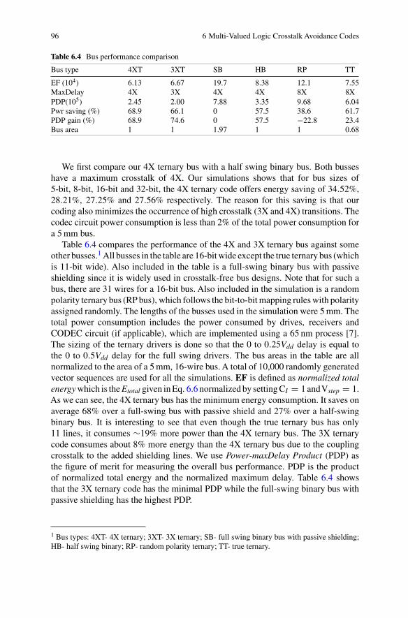
96 6 Multi-Valued Logic Crosstalk Avoidance Codes
Table 6.4 Bus performance comparison
Bus type 4XT 3XT SB HB RP TT
EF (104) 6.13 6.67 19.7 8.38 12.1 7.55MaxDelay 4X 3X 4X 4X 8X 8XPDP(105) 2.45 2.00 7.88 3.35 9.68 6.04Pwr saving (%) 68.9 66.1 0 57.5 38.6 61.7PDP gain (%) 68.9 74.6 0 57.5 −22.8 23.4Bus area 1 1 1.97 1 1 0.68
We first compare our 4X ternary bus with a half swing binary bus. Both busseshave a maximum crosstalk of 4X. Our simulations shows that for bus sizes of5-bit, 8-bit, 16-bit and 32-bit, the 4X ternary code offers energy saving of 34.52%,28.21%, 27.25% and 27.56% respectively. The reason for this saving is that ourcoding also minimizes the occurrence of high crosstalk (3X and 4X) transitions. Thecodec circuit power consumption is less than 2% of the total power consumption fora 5 mm bus.
Table 6.4 compares the performance of the 4X and 3X ternary bus against someother busses.1 All busses in the table are 16-bit wide except the true ternary bus (whichis 11-bit wide). Also included in the table is a full-swing binary bus with passiveshielding since it is widely used in crosstalk-free bus designs. Note that for such abus, there are 31 wires for a 16-bit bus. Also included in the simulation is a randompolarity ternary bus (RP bus), which follows the bit-to-bit mapping rules with polarityassigned randomly. The lengths of the busses used in the simulation were 5 mm. Thetotal power consumption includes the power consumed by drives, receivers andCODEC circuit (if applicable), which are implemented using a 65 nm process [7].The sizing of the ternary drivers is done so that the 0 to 0.25Vdd delay is equal tothe 0 to 0.5Vdd delay for the full swing drivers. The bus areas in the table are allnormalized to the area of a 5 mm, 16-wire bus. A total of 10,000 randomly generatedvector sequences are used for all the simulations. EF is defined as normalized totalenergy which is the Etotal given in Eq. 6.6 normalized by setting CI = 1 andVstep = 1.As we can see, the 4X ternary bus has the minimum energy consumption. It saves onaverage 68% over a full-swing bus with passive shield and 27% over a half-swingbinary bus. It is interesting to see that even though the true ternary bus has only11 lines, it consumes ∼19% more power than the 4X ternary bus. The 3X ternarycode consumes about 8% more energy than the 4X ternary bus due to the couplingcrosstalk to the added shielding lines. We use Power-maxDelay Product (PDP) asthe figure of merit for measuring the overall bus performance. PDP is the productof normalized total energy and the normalized maximum delay. Table 6.4 showsthat the 3X ternary code has the minimal PDP while the full-swing binary bus withpassive shielding has the highest PDP.
1 Bus types: 4XT- 4X ternary; 3XT- 3X ternary; SB- full swing binary bus with passive shielding;HB- half swing binary; RP- random polarity ternary; TT- true ternary.

6.4 Experimental Results 97
Fig. 6.5 Crosstalk distributions
Figure 6.5 shows the distribution of the crosstalk for several different types ofbusses. We can see that by applying our coding scheme, the distribution of thetransitions shift towards lower Xeff values. The true ternary bus has fewer total numberof transitions compared to the other busses since there are fewer bits on the trueternary bus (11-bits). However, a significant portion of the transitions have 4X andhigher crosstalk. The total energy consumption is therefore higher than either codedternary bus.
We implemented the voltage-mode ternary bus and verified the delay for differentXeff values in SPICE simulation. The results are given in Table 6.5 and as expected,we note that the delay scales roughly linearly with Xeff . Again, we use a 65 nm CMOSprocess model in the simulation [7], with wiring dimensions and parasitics obtained
Table 6.5 Delay vs. Crosstalk
Driver size 30X 30X 60X 60X
Bus length 5 mm 10 mm 10 mm 20 mm
Crosstalk Delay (ns)
0X 25 110 60 651X 110 220 140 2002X 190 350 230 3503X 300 580 350 5904X 420 790 460 7605X 520 970 530 9606X 630 1140 640 11307X 730 1260 750 12908X 810 1390 850 1430

98 6 Multi-Valued Logic Crosstalk Avoidance Codes
Fig. 6.6 Ternary bus eye-diagrams a Uncoded ternary bus b 4X ternary bus
from [61]. Figure 6.6 shows the eye diagrams for a uncoded and a 4X ternary bus.Note that the eye is more open for the 4X ternary bus.
6.5 Summary
At the beginning of this chapter, we derived delay and power consumption expres-sions for multi-valued busses and generalized the crosstalk-based bus classificationfor such busses. We then designed two ternary bus coding schemes to limit max-imum crosstalk on a ternary bus. Both coding schemes simultaneously lower thepower consumption and boost the speed of on-chip bus interconnects. The proposed4X bus effectively improves the bus speed by ∼100% compared to a true ternary busor a full-swing binary bus, with no area overhead compared to a binary bus. The 3Xbus offers an additional 33% speed increase with a 20% area overhead.
Our simulation results show that the 4X ternary bus with the proposed crosstalkavoidance coding schemes exhibits on average over 27% power saving over a binary

6.5 Summary 99
bus with half swing, and over 68% lower power consumption than a full swing binarybus with passive shielding. Compared to a true ternary bus, the coded ternary bus canoperate at over twice the speed and exhibits over 11% power saving. The encoderand decoder for both the proposed coding schemes can be implemented with verysimple logic thanks to the simplicity and regularity of the coding logic and the useof direct bit-to-bit mapping between binary data words and ternary codes.
We also presented low power designs for the ternary driver and receiver cir-cuits. We also proposed an efficient low impedance on-chip power supply gen-erator, that when used with our voltage mode bus, reduces the static powerconsumption.

Chapter 7Summary of On-Chip Crosstalk Avoidance
Conventional wisdom doubts that bus encoding would ever become a viable solutionto the problem of inter-wire capacitive crosstalk due to its area overhead and CODECcomplexity associated with such techniques.
In Part I, we presented some of the recent research in overcoming these obstaclesand showed that such techniques can be highly efficient.
Following a brief overview of techniques in crosstalk avoidance at the beginningof Part I , we examined the phenomenons of crosstalk in on-chip busses and illustratedthat capacitive coupling between adjacent parallel bus wires is the main contributor tothe speed and power degradation in deep sub-micron signal busses. We introduced thenotion of effective capacitance and showed that both delay and energy consumptionof busses are linearly proportional to it. We introduced a bus classification systemfor binary busses to make the subsequent discussion clear. This classification systemwas later generalized to multi-valued busses.
With the establishment of this classification system, we introduced our first setof crosstalk avoidance codes—memoryless codes. These codes have the inherentadvantage of requiring simpler CODECs. We showed that there exists a trade offbetween the area overhead and the speed-up factor for all the codes. Generally, thehigher the speed-up, the larger the area overhead. Some of the memoryless codes wediscussed include the FPF code (3C-free) [36], FTF code (3C-free code proposedby B. Victor [100]), 2C-free code and 1C-free configurations [35]. We showed thatmathematical induction based approaches can be used to effectively generate code-words for both 3C-free codes and the 2C-free code. Such inductive approaches alsoallow us to compute the code cardinality without explicitly enumerating all the code-words. We found that based on our computation, 3C-free memoryless codes require∼44% overhead, which is significantly lower than the conventional static shieldingapproaches. The overhead is higher for 2C-free codes but still lower than shieldingtechniques.
As part of a complete solution for memoryless codes, we also discussed in de-tail some efficient CODEC design approaches for these codes. The bus-partitionbased solution is simple and allows us to control the CODEC size and speed.Our solutions based on the Fibonacci Numeral System are advantageous overconventional solutions because of their significantly reduced area, simple design,
C. Duan et al., On and Off-Chip Crosstalk Avoidance in VLSI Design, 101DOI 10.1007/978-1-4419-0947-3_7, © Springer Science+Business Media LLC 2010
102 7 Summary of On-Chip Crosstalk Avoidance
deterministic mapping, reusable modular structure and most importantly, the extremelow complexity and high speed.
We also investigated memory-based codes and showed that they are more efficientin terms of area overhead. A 4C-free code design was given as one of the simplestmemory-based code, with a 33% overhead. We showed that graph pruning can beused to represent codewords and transitions. Based on a graph representation, weshowed that codeword pruning is a simple way of finding the minimum encodingoverhead. It, however, requires a large amount of memory and run time. We proposedan ROBDD-based approach that represents all the illegal code words canonicallyand generates codewords efficiently. It also suffers from the same limitations as thecodeword pruning technique. As a result, realistic memory based CACs would needto partition large busses into smaller groups.
Finally, we investigated the crosstalk avoidance coding for multi-valued busses.We first generalized the classification system into the multi-valued realm and showedthat the speed and power of a bus are related to the effective crosstalk coefficient,Xeff, a parameter defined in a manner similar to the effective capacitance Ceff inthe binary bus case. Noting that the supply voltages are scaling down continuously,using more than 4 values in a multi-valued bus is impractical. Hence, we proposedtwo code designs specifically for the ternary bus. These codes use a bit-to-bit directmapping which makes the encoding and decoding trivial. By allowing flexibility onthe signal polarity and establishing a few coding rules, the encoded busses eliminatebus patterns with high crosstalk and significantly reduce the probability of otherhigh crosstalk patterns. These codes exploit the low signal swing of the multi-valuedsignals. As a result, we were able to achieve a significant speed improvement andpower saving.
We believe that the issue of crosstalk avoidance in on-chip interconnect to reducedelay and power will attract more and more attention as the technology marchesahead. Beyond the research presented in this monograph, there is room for furtherimprovement. For example, efficient CODEC design for memory-based codes isa subject worth further investigation. Multi-valued logic based bus interconnect isanother area that holds significant promise. Crosstalk in serial busses is also animportant topic. Even though there have been several publications on combiningcrosstalk avoidance codes with other codes such as forward error correction codes,an practical, efficient design has yet to be discovered.
Some of the techniques discussed are not limited to bus crosstalk avoidance,instead, they can be applied to other areas. For example, the FPF code can be of partic-ular interest to certain applications in digital communication, where certain patternsare designated to carry higher priority messages, such as emergency massages. OurFPF codes have 44% overhead, which is much less compared to existing schemes.The FPF code may also be used in serial data communications, in which back to backtoggles are not allowed. Another potential applications is interference managementin wireless communications. The transmission in a cell (or sector) is considered asinterference to an adjacent cell (or sector). The accumulated interference can greatly

7 Summary of On-Chip Crosstalk Avoidance 103
reduce the capacity of the victim cell. It is conceivable that some of the crosstalkavoidance schemes may be applied for interference management. Another interestingproperty of the FPF code lies in its spectrum. Since the high frequency componentare suppressed, we expect that by applying FPF encoding, high bandwidth effi-ciency can be achieved. This is extremely valuable for many wireless communicationsystems.

Part IIOff-Chip Crosstalk and Avoidance

Chapter 8Introduction to Off-Chip Crosstalk
Integrated circuit (IC) performance has increased at an exponential rate since the firstpatent was issued to Robert Noyce of Fairchild Semiconductor in 1961 [10]. Sincethe advent of the IC, the number of transistors on an integrated circuit has roughlydoubled every 18 months. This trend, also known as Moore’s Law [96], has beenconsistently met over the past 45 years. This increase in system performance on theIC is predicted by the International Technology Roadmap for Semiconductors (ITRS)[11] to continue to follow Moore’s Law into the foreseeable future. Historically, thegate delay of the digital circuitry has limited IC performance [59]; however, over thepast decade the bottleneck of system performance has shifted from the gate delay ofthe integrated circuit to the package parasitics [96]. While package performance hassteadily improved, it has not kept pace with the increases in integrated circuit perfor-mance. Package performance is predicted by the ITRS to only double over the nextdecade. This imbalance in performance expectations between the IC and the packageis a major concern for system designers and for the continuation of Moore’s Law.
The limitation in package performance comes from the parasitic inductance andcapacitance in the electrical interconnect [32, 57, 96]. Package interconnect hashistorically been designed to meet mechanical, thermal, and cost objectives. In thepast, the electrical performance of the interconnect was not an issue since it caused arelatively small performance degradation relative to the gate delay of the IC transis-tors [59]; however, with the dramatic improvement in transistor gate delay, packageperformance is now the leading determinant of the overall system performance.
8.1 The Role of IC Packaging
The purpose of an IC package is to electrically and mechanically connect the inte-grated circuit substrate to the system substrate. The most common substrate used inVery Large Scale Integrated (VLSI) circuitry is silicon [59]. Silicon offers a host ofelectrical advantages that allow the implementation of large numbers of transistorsin a cost-effective and easy-to-manufacture manner. In VLSI silicon designs, con-ductors are most commonly implemented using Polysilicon (p−Si), Aluminum (Al),and Copper (Cu). Insulating layers in VLSI designs are typically implemented using
C. Duan et al., On and Off-Chip Crosstalk Avoidance in VLSI Design, 107DOI 10.1007/978-1-4419-0947-3_8, © Springer Science+Business Media LLC 2010

108 8 Introduction to Off-Chip Crosstalk
Silicon Oxide (SiO2) and Silicon Nitride (Si3N4). The photolithography and deposi-tion processes used in IC fabrication allow extremely small feature sizes to be printedon the substrate. Currently, feature sizes as small as 65 nm are being successfullyimplemented using VLSI processes [84].
System level interconnect in digital systems is typically constructed using printedcircuit board (PCB) technology [32]. PCBs typically use Copper as their conductinglayer. Insulating layers are implemented using dielectric materials such as FR4,Nelco-13, GETEK®, and Teflon. PCBs are constructed using a lamination pro-cess. Modern lamination processes are capable of producing minimum feature sizesbetween 4 and 100 μm.
An IC package serves many purposes. The first is to electrically connect the leadson the IC to the corresponding leads on the system PCB. Since the feature sizeson the IC are much smaller than the feature sizes on the PCB, the IC cannot bemounted directly to the system PCB. The package serves as a density translatorfor the electrical signals that will connect extremely fine-pitch signals on the IC tocoarser-pitched signals on the PCB.
The second purpose of the package is to protect the substrate of the IC. The ICsubstrate consists of a very thin crystal of silicon that has transistors and interconnectdeposited on it. This substrate is brittle and can be easily fractured, leading to circuitfailure [96]. The package serves as a mechanical barrier and hermetic seal betweenthe silicon substrate and the outside environment. In this manner the substrate isisolated from contamination and humidity, which can also lead to IC failures. Inaddition, the package absorbs thermal expansion mismatches between the siliconsubstrate and the system PCB. If the thermal mismatches were completely absorbedby the silicon substrate, it would lead to stress fractures and circuit failure.
The third major purpose of IC packaging is to remove heat from the IC substrate.Modern ICs consist of millions of transistors that each consume current and dissipatepower. The cumulative power dissipation of the transistors lead to the generation ofextreme amounts of heat in a relatively small area. This high thermal density ad-versely effects circuit performance by increasing the gate delay and shortening thelife of the devices on the IC [59]. The typical range of operating junction tempera-tures for modern VLSI designs is between 80◦C and 120◦C on the silicon substrate[40, 59]; however, modern microprocessors are projected by the ITRS to surpassthe 100 Watt power dissipation mark within the next couple of years [40]. All thispower is dissipated by substrates that range from 5 to 20 mm2 in size [54, 62]. Thepackage serves as a heat transfer system that removes the heat from the IC substrate.The heat is delivered to a package surface from which it can ultimately be absorbedby ambient air. By doing this, the package can keep the circuitry on the IC within theacceptable range of junction temperatures. This leads to consistent and predictableperformance of the devices on the IC substrate.
Historically, the thermal and mechanical aspects of the package were the mainfocus of the package design [96]. Since the gate delay of the devices on the ICwere the largest source of performance limitation, the electrical interconnect in thepackage was optimized for mechanical and thermal purposes. This approach hasbeen successful for the past 40 years. Only recently has the electrical interconnect in
8.2 Noise Sources in Packaging 109
the package become the bottleneck to system performance. This has occurred due tothe dramatic advances in integrated circuit technology that has reduced the gate delayof the on-chip devices to the point where they no longer limit system performance.This shift as resulted in the package (which was originally optimized for mechanicaland thermal rather than electrical consideration) becoming the major limiting factorin system level electrical performance.
The electrical interconnect limits performance due to the parasitic resistance,inductance and capacitance that is present in the interconnect structure [32, 57, 58].Since the interconnect structures were originally created for mechanical properties,their parasitic inductance and capacitance can be considerable relative to the dataratesthat are currently being transmitted through the package. Package design is a slowand expensive process that has not been able to keep pace with the performanceincrease in core IC technology. This makes the task of altering the interconnectstructures within the package (to increase electrical performance) very difficult. Themajority of VLSI designs today cannot afford the cost and time associated with re-engineering a package [40]. This means that in most cases designers must live withthe performance limitations in the package. Any technique that can increase systemperformance without changing the package design is of tremendous value to theVLSI community.
8.2 Noise Sources in Packaging
Electrically the package has two objectives. The first is to deliver power to the deviceson the integrated circuit. The power resides on the system PCB and must be conductedthrough the package to the devices on-chip. The second objective is to connect signalson the IC to the signal paths on the system PCB. In both of these cases electricalcurrent and voltage are carried using interconnect structures within the package thatwere not originally optimized for electrical performance. The parasitic resistance,inductance and capacitance of these structures limits how efficiently the power canbe delivered and how fast the signals can be transmitted.
8.2.1 Inductive Supply Bounce
When inductance is present in the path that carries power to the devices on the IC, avoltage will form across this inductance based on the relationship:
VL = L ·(
di
dt
)(8.1)
In the case of power delivery, the inductance in Eq. 8.1 is the parasitic inductance inthe interconnect structure that carries current to and from the devices on-chip. ( di
dt )is the rate of change of the current that is carried through the interconnect. As moreand more transistors are integrated on-chip, the total amount of current that is being

110 8 Introduction to Off-Chip Crosstalk
carried through the interconnect increases. In addition, as the operating frequencyof the digital circuits increase, the time in which this current is delivered is reduced.This results in significant increases in the rate of change of current ( di
dt ) through thepackage interconnect. These two trends are being driven by the increase in IC tech-nology; however, the inductance (L) present in the interconnect is driven by packagetechnology, which is not improving at a rate which would keep di
dt unchanged [11].When a voltage is induced across the power supply interconnect, the voltage on
the chip will be different from the voltage on the system PCB. When delivering apower supply voltage (VDD) to a CMOS device, there will be a voltage drop betweenthe system PCB and the integrated circuit. This phenomenon is called supply bounce.Similarly, when the ground return current for a CMOS device traverses an inductiveinterconnect, a voltage will be induced across the inductive interconnect (causing thevoltage at the ground pin of the device (VSS) to be different from the system PCB).Thisphenomenon is called ground bounce. Supply and directly effect the performanceof the digital device by increasing its gate delay and causing inadvertent switching[59]. Figure 8.1 shows an ideal CMOS inverter. In this circuit, the on-chip powersupplies VDD and VSS are assumed to be the same as on the system PCB. Figure 8.2shows a CMOS inverter but models the inductance in the supply and ground path. Inthis case, the voltage from Eq. 8.1 (induced across the inductive interconnect) resultsin a voltage difference between the supply nodes of the device (VDD–IC, VSS–IC) andthe supply voltages on the system PCB (VDD–System, VSS–System).
In modern VLSI designs, between 25 to 50% of the total ( didt ) can be consumed
in the off-chip driver circuitry and constitutes the largest single source of currentconsumption [11, 40]; however, VDD and VSS pins are often shared across multiplesignal pins that are drawing and returning current for their off-chip driver circuitry.Supply pins are shared to reduce the cost of the package since cost is proportional tothe size of the package. Therefore, in order to accurately compute the magnitude ofthe supply and ground bounce we must modify Eq. 8.1 to consider all of the signal
Fig. 8.1 Ideal CMOS inverter circuit
Vin
M2 (pmos)
Vout
M1 (nmos)
VSS
VDD

8.2 Noise Sources in Packaging 111
Fig. 8.2 CMOS inverter circuitwith supply inductance
Vin
M2 (pmos)
Vout
M1 (nmos)
VSS - System
VDD - System
VDD - IC
Lint
VSS - IC
Lint
pins that are sharing a supply pin to source or return current. For supply bouncethe total number of signals (which share a given VDD pin) that are switching froma 0 to a 1 must be considered. Equation 8.2 expresses the total amount of powersupply bounce considering all signals that are drawing current through the supplypin inductance. For, the total number of signals that are switching from a 1 to a 0and are sharing a particular VSS interconnect to return current must be considered.Equation 8.3 expresses the total amount of ground bounce considering all signalsthat are returning current through the ground pin inductance.
VSupply–Bounce = L(VDD) ·n(0→1)∑
k=0
(dikdt
)(8.2)
VGround–Bounce = L(VSS) ·n(1→0)∑
k=0
(dikdt
)(8.3)
8.2.2 Inductive Signal Coupling
When a signal traverses an inductive interconnect in a package it inductively couplesto neighboring signals. This is due to the mutual of the magnetic fields for any twocurrent carrying conductors. The magnitude of the mutual inductive coupling voltagebetween inductive interconnects is governed by the expression:
VjM = M1k ·
(dikdt
)(8.4)

112 8 Introduction to Off-Chip Crosstalk
M1k is the mutual inductance between conductor j and conductor k. This relationshipcan also be expressed in terms of the mutual inductive coupling coefficient Kik . K1k
is a dimensionless quantity. Equation 8.5 describes the relationship between M1k andK1k . In this expression, Lj and Lk are the inductances of the two inductively coupledconductors.
K1k = M1k[√Lj · Lk
] (8.5)
For this work we use the term victim for the signal of interest (on which the mutualinductive voltage is induced). We use the term aggressor for any neighboring signalthat switches and causes a voltage to be induced on the victim. Mutual inductivecoupling has a cumulative effect in IC packaging. The mutually induced voltage isalso dependent on the polarity of the ( di
dt ) in the aggressor’s signal path. This meansthat the total mutual inductive voltage on the victim is the sum of all aggressors’mutually coupled voltage. This unique circumstance creates a situation in whichthe switching patterns of neighboring signals heavily influence the behavior of thecoupled noise on the victim signal. In an extreme case, the aggressors’ mutuallycoupled voltage (of equal and opposite magnitudes) can cancel out and have noeffect on the victim. Equation 8.6 describes the total contribution of mutually coupledvoltages on a victim signal.
VjM =
n∑
k=1
M1k ·(
dikdt
)(8.6)
We define the term Glitch to describe the situation in which the victim signal is nottransitioning and neighboring signal pins are coupling voltage onto it. The Glitchvoltage caused by switching aggressor signals creates an unwatched voltage on thevictim signal. This unwanted voltage can lead to inadvertent switching of digitalcircuitry that use the victim line as an input.
When the victim signal is transitioning, we use the term Edge Degradation todescribe the effect of voltage that is coupled from neighboring aggressor signals.Since mutual inductive coupling is cumulative, coupled voltage from neighboringsignals can have the effect of aiding, hindering, or not affecting the transition on thevictim signal. Figure 8.3 shows the circuit for inductively coupled signal lines in aVLSI package.
Fig. 8.3 Circuit descriptionof inductive signal coupling
Vaggr
M1k
Vvic
Vaggr

8.2 Noise Sources in Packaging 113
8.2.3 Capacitive Bandwidth Limiting
When capacitance is present along the path that carries signals to and from thedevices on the IC, the frequency at which the signal can switch will be reduced. Thiscapacitance will form a low pass RC filter that will prevent frequency componentsthat are above the filters roll-off frequency from passing through the interconnect.This filtering effect will limit the risetime that the package will allow to pass andin turn reduce the overall datarate and performance of the system. The filter thatthe package creates in the signal path has a standard RC low pass response. Thecapacitance in the filter comes from the parasitic capacitance present in the packageinterconnect. The impedance in the filter comes from the characteristic impedance ofthe system in which the package is placed. Equation 8.7 gives the 10–90% risetimeof a single-pole RC filter.
trise = 2.2 · RC = 2.2 · Z0 · Cint (8.7)
In this expression Z0 is the of the system in which the package is placed. Cint repre-sents the total capacitance that the package interconnect presents. Cint will dependon the parasitic capacitance of the interconnect to ground (C0) in addition to theparasitic capacitance to neighboring signals (C1j). The total number of neighboringsignals that contribute capacitance to Cint must be accounted for. Equation 8.8 givesthe total amount of capacitance that an individual package interconnect possesses.
Cjtotal = C0 +
n∑
k=1
C1k (8.8)
The logic level of neighboring signals will affect the amount of capacitance that avictim signal will have to charge or discharge (C1k). C1k is defined as the capacitancebetween two conductors when one conductor is held at zero potential. Capacitanceis defined as C = Q/V . This means that the variable voltage that is present onneighboring signals will change the effective capacitance of the victim signal. Whena neighboring signal has the same voltage change as the victim signal (i.e., theyare transitioning), then the total coupling capacitance between signals will be zerobecause there is no net charge difference between the two conductors. When a neigh-boring signal has a static voltage value while transitioning, then the total couplingcapacitance between the signals will be C1k . When a neighboring signal transitionsin the opposite direction as the victim signal, then the total effective coupling capac-itance will be 2 · C1k because the voltage excursion that the capacitor undergoes is2 · VDD.1 This situation means that the risetime of a signal will change depending onthe logic levels and transitions present on neighboring signals. Figure 8.4 shows thecircuit diagram for a signal with capacitive bandwidth limitation.
1 The voltage across the capacitor is −VDD before the transition and +VDD after the transition (orvice versa).

114 8 Introduction to Off-Chip Crosstalk
Fig. 8.4 Circuit description ofcapacitive bandwidth limiting
V
C1k
V1
C0
Vk
C1k
Vk
8.2.4 Capacitive Signal Coupling
When a signal traverses a capacitive interconnect in a package, it is electricallymodified due to coupling from neighboring signals. This is due to the mutual of theelectric fields for any two charge bearing surfaces. The magnitude of the mutualcapacitive coupling voltage between capacitive interconnects will depend on thecoupling capacitance between the conductors (C1k) in addition to the self-capacitance(C0) of the victim line. The sum of the coupling capacitance, along with the self-capacitance of the victim line will form a capacitive voltage divider between thevictim and aggressor lines. Equation 8.9 describes the voltage magnitude that will becoupled onto a victim line (Vvic) from a voltage change on an aggressor line (Vaggr).
Vvic =(
C1k
C1k + C0
)·(�Vk
aggr
)(8.9)
Capacitive coupling can cause unwanted switching of digital circuitry, which limitssystem performance. As in the case of mutual inductive coupling, the capacitivecoupling has a cumulative effect. Glitches on a victim line that occur due to thetransitions on neighboring signals can cause unwanted switching of digital circuitry.Also, the cumulative nature of the coupling will lead to an effect that can either aid,hinder, or not effect the victim signal’s risetime. Equation 8.10 models the cumulativenature of the capacitive coupling betweens signals. Figure 8.5 shows the circuit forcapacitively coupled signal lines in a VLSI package.
Vvic =n∑
k=1
(C1k
C1k + C0
)·(�Vk
aggr
)(8.10)

8.2 Noise Sources in Packaging 115
Fig. 8.5 Circuit description ofcapacitive signal coupling
Vaggr
C1k
C0
Vvic
Vaggr
8.2.5 Impedance Discontinuities
Another source of noise in the package interconnect is reflected energy due to impe-dance discontinuities. As the risetimes of off-chip driver circuits increase, conduc-tors must be considered as distributed elements. Typically when the interconnectbeing driven has an electrical length2 that is longer than 20% of the risetime of thesource, then the conductor must be treated as a distributed element and modeled asa transmission line [57]. Current off-chip risetimes are entering into the sub 100psera. For standard packaging technology this means that a structure longer than 1 to2 cm must be treated as a distributed element. For these electrical lengths almost allmodern packages require the use of transmission line theory for accurate modelingof the package interconnect.
When IC packaging interconnect is treated as a distributed element, becomescritical. When impedance mismatches are present in the package, reflections andrisetime degradation will occur. The reflections can lead to unwanted switching ofdigital circuitry and intersymbol interference (ISI). In addition, risetime degradationwill significantly limit system performance. The characteristic impedance of a loss-less structure is given by:
Z0 =√
L
C(8.11)
In this expression the L and C are the inductance and capacitance of a given structure.When considering the impedance of the package, the switching patterns of neighbor-ing signals will alter the inductance and capacitance in Eq. 8.11. Switching signalpins will add or subtract additional amounts of mutual inductance and capacitanceto the victim signal. These additional parasitics must be considered in the evaluationof characteristic impedance. This changes the impedance within the package to:
Z ′0 =
√√√√L ±∑k1 M1k
C ±∑k1 C1k
(8.12)
2 Propagation delay of the structure.

116 8 Introduction to Off-Chip Crosstalk
Fig. 8.6 Circuit descriptionof a distributed transmissionline
V
Z0 ZL
When a wave front is traveling on a conductor with a particular characteristicimpedance (Z0) and encounters a region with a different characteristic impedance(ZL), reflections will occur. Figure 8.6 shows the circuit diagram for a distributedtransmission line.
� is the reflection coefficient which represents the magnitude of the reflectedvoltage (as a fraction of the incident voltage) and is defined as:
� = ZL − Z0
ZL + Z0(8.13)
� can be used to find the reflected and transmitted voltage of an incident wave front.Equation 8.14 defines the amount of reflected voltage due to an impedance mismatch.This Equation illustrates the relationship between an impedance mismatch and themagnitude of the reflected voltage. Note that the reflected voltage can have eithera positive or negative amplitude depending on whether ZL is greater than or lessthan Z0.
Vreflected = Vincident · � (8.14)
Equation 8.15 defines the amount of transmitted voltage when encountering animpedance mismatch. In this case the magnitude of the reflected voltage will besubtracted from the forward going wave front. This translates into a slower risetimethat is propagated through the impedance mismatch. Since risetimes are directlyproportional to the datarate that a package can achieve, any reduction in the risetimedue to reflected energy will directly effect system performance.
Vtransmitted = Vincident · (1 − �) (8.15)
In digital systems typically the system PCB uses a close to 50 �. The interconnectstructures within the IC package typically do not match to the system PCB impedanceand will lead to reflections. When the impedance of a package structure is higherthan the characteristic impedance of the system (50 �), it is considered an inductiveinterconnect. It is considered to be inductive because in Eq. 8.12 a higher thanoptimal inductance will lead to a higher impedance. In the same manner, whenthe impedance of a package structure is lower than the characteristic impedance ofthe system, it is considered a capacitive interconnect. Since current packages were

8.3 Performance Modeling and Proposed Techniques 117
originally designed for mechanical considerations, getting a desired impedance isdifficult without using expensive and non-standard processes.
As in the case with capacitive bandwidth limitation, switching neighboring pinswill alter the net coupling inductance and capacitance that the victim pin experi-ences. The polarity and quantity of switching signals will alter the effective L and Cquantities in Eq. 8.12 and in turn the magnitude of �.
8.3 Performance Modeling and Proposed Techniques
All of the noise sources described in Sect. 8.2 can be reduced through aggressivepackage design. We have seen success in Ball Grid Array (BGA) [51] and Flip-chippackaging [53] technologies that have been able to reduce the electrical parasiticsof the interconnect structures within the IC package; however, aggressive packagedesign is often too expensive and unpractical for the majority of VLSI designs. Inaddition, package design is a slow, evolutionary process that is not predicted to keeppace with the performance increases on the IC. As such, any techniques that canassist in improving performance without moving toward advanced packaging are ofconsiderable value to the VLSI community. In addition, such techniques that modelthe general RLC parasitics of the package can be used to increase the performanceof the package, and extend the useful lifetime of the package.
8.3.1 Performance Modeling
In all the noise sources in Sect. 8.2, the amount of noise is ultimately proportionalto the rate of change of the current or voltage ( di
dt or dvdt ). The rate of change of
current or voltage can be translated to system performance using standard equationsfor robust high-speed digital design [57]. Since all of the noise sources are expressedin terms that relate the amount of noise to the rate of change in current or voltage, theacceptable rate of change of voltage or current can be calculated. Using this approachthe maximum system performance can be predicted using the electrical packageparameters and user-defined noise limits as the two inputs into the model. In this workan analytical model is proposed for system performance which considers each noisesource. From this model the maximum rate of change of voltage or current can befound for any given package and set of noise limits. This directly predicts the per-pindatarate and ultimate bus throughput for a given package. This analytical model is alsoused to predict the performance increase for the various solutions that are presented.The performance model presented in this work is shown to be accurate to within 10%of analog simulator results which are much more computationally expensive.
8.3.2 Optimal Bus Sizing
One of the biggest challenges for VLSI designers is selecting the size and configu-ration for their off-chip busses [40]. The main problem is that simply adding pins toan off-chip bus does not necessarily increase the throughput in a linear manner [49].

118 8 Introduction to Off-Chip Crosstalk
As pins are added to a package to increase the bus size and throughput, the noise in-duced by the signals that are simultaneously switching leads to a significant increasein noise. This means that as signals are added, the per-pin datarate of each pin needs tobe decreased to meet the system noise limits. As a result, the overall throughput of anoff-chip bus approaches an asymptotic limit as signals are added. As a consequence,multiple bus configurations can meet the same throughput objective. In order to aid inthe selection of the optimal bus configuration, the cost of the bus is considered in themodel. By including the cost of the signal, power, and ground pins that are needed toexpand the size of a bus, the most cost-efficient bus configuration can be found. Thisallows designers to quickly compare two bus configurations of equal throughput andchoose the least expensive solution. The model considers the electrical parametersof the package in addition to the per-pin cost, which allows the model to compareconfigurations in different packages. The metric of Bandwidth per Cost is definedas a means to find the most cost-effective bus configuration. The results presentedin this work are supported by the industry trend of moving toward faster narrowerbusses over slower wider busses to achieve the same throughput at a lower cost.
8.3.3 Bus Encoding
When determining the maximum performance of a bus the worst-case noise limitsmust be considered. In all of the noise sources listed in Sect. 8.2, a worst-case buspattern is assumed to be present on the bus. In the case of supply bounce all of thesignals in the bus are assumed to be switching in the same direction. In the caseof bandwidth limitation and signal coupling, the middle signal in the bus is eitherswitching in one direction while all of the other signals on the bus are switching inthe opposite direction, (Edge Degradation) or the middle signal is static while allother signals are switching in the same direction (Glitch). This work presents twobus encoding techniques that encode the off-chip data prior to leaving the IC. Theencoding ensures that all patterns that result in noise of a magnitude greater than auser-specified limit are eliminated. By doing this a lower level of noise in the systemis achieved which translates into increased performance. The techniques presentedin this work show that the performance of the bus is increased dramatically even afterconsidering the overhead of the encoder algorithm.
The first encoding technique is called Bus Expansion which maps the original setof logic vectors on the IC into an expanded set of vectors prior to leaving the IC.This expanded set of vectors ensures that noise patterns of a magnitude greater thanthe user-specified limit are never present on the data that is traversing the package.
The second encoding technique is called Bus Stuttering, which uses the originalnumber of package pins but avoids the worst-case noise patterns by inserting inter-mediate logic vectors between outgoing pairs of vectors that induce noise with amagnitude greater than the user-specified limit. This approach allows the algorithmto be tailored for packages that are dominated by interconnect that is inductive, capac-itive, or both. Experimental results show that the encoder circuits can be integratedinto a modern CMOS process and achieve a minimal delay and area impact on the

8.3 Performance Modeling and Proposed Techniques 119
design. The encoders are shown to improve performance of off-chip busses up to225% by avoiding data patterns which result in noise violations.
8.3.4 Impedance Compensation
Impedance discontinuities are caused by excess inductance or capacitance that ispresent in the package interconnect. The term excess refers to any inductance orcapacitance that causes the interconnect impedance to be different from the systemimpedance. If the interconnect has a higher impedance than the system (ZL > Z0),then the interconnect is said to have excess inductance. If the interconnect has alower impedance than the system (ZL < Z0), then the interconnect is said to have ex-cess capacitance. When this occurs, the impedance discontinuities cause reflectionswhich limit the performance of the system. To address this problem a compensationtechnique is presented that adds capacitance or inductance near the interconnect tomatch its impedance to the system impedance. If the spatial location of the com-pensation inductance/capacitance is near the interconnect, then the interconnect andcompensation will be seen as a lumped element and will be governed by Eq. 8.12.By using this compensation technique, a forward traveling wave front will see thecompensated package interconnect as a matched impedance and reflections will beavoided.
Two compensation techniques are presented in this work. The first technique is astatic compensation approach in which the pre-defined compensation elements areplaced on the package and IC substrate. This technique surrounds the interconnectwith the appropriate inductance or capacitance to achieve the impedance match.
The second technique is a dynamic compensation approach in which programm-able compensation elements are placed on-chip. By placing the compensation on-chip, the interconnect impedance can be adjusted after the IC is packaged. This hasthe advantage of being able to accommodate any design or manufacturing tolerancesthat may vary the interconnect’s original impedance. Both techniques are shown to beable to compensate for all reasonable ranges of package interconnect impedance andsignificantly reduce reflections. The compensation techniques are shown to reducereflected noise as much as 400% for broadband frequencies up to 3 GHz.
Figure 8.7 show a summary of the improvement in bus performance that can beachieved using the techniques proposed in this work. The original performance isbased on a bus size of 4 bits with one VDD and one VSS pin where supply bounce isthe failure mechanism. The performance is improved by encoding the data to avoiddata patterns which result in noise limit violations and in turn limit the maximumthroughput that can be achieved. The performance improvement considers the over-head of the encoder. For all package technologies studied in this work, the supplybounce due to the inductive nature of the interconnect is the limiting factor. Movingtoward advanced packaging reduces the parasitic inductance present in the packagewhich results in faster performance. In addition, when the parasitics of the packageare reduced, the improvement techniques presented in this work will have more of apositive impact.
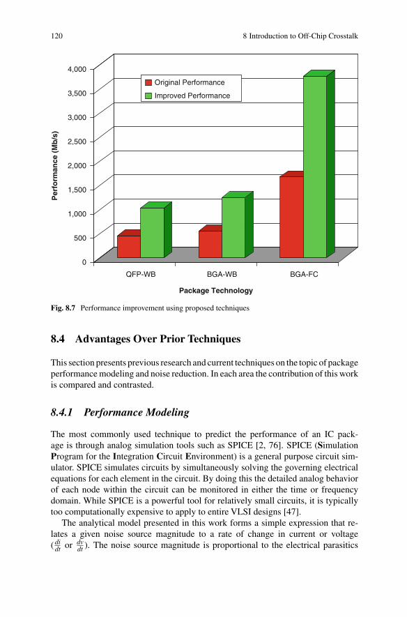
120 8 Introduction to Off-Chip Crosstalk
0
500
1,000
1,500
2,000
2,500
3,000
3,500
4,000
Per
form
ance
(M
b/s
)
QFP-WB BGA-WB BGA-FC
Package Technology
Original Performance
Improved Performance
Fig. 8.7 Performance improvement using proposed techniques
8.4 Advantages Over Prior Techniques
This section presents previous research and current techniques on the topic of packageperformance modeling and noise reduction. In each area the contribution of this workis compared and contrasted.
8.4.1 Performance Modeling
The most commonly used technique to predict the performance of an IC pack-age is through analog simulation tools such as SPICE [2, 76]. SPICE (SimulationProgram for the Integration Circuit Environment) is a general purpose circuit sim-ulator. SPICE simulates circuits by simultaneously solving the governing electricalequations for each element in the circuit. By doing this the detailed analog behaviorof each node within the circuit can be monitored in either the time or frequencydomain. While SPICE is a powerful tool for relatively small circuits, it is typicallytoo computationally expensive to apply to entire VLSI designs [47].
The analytical model presented in this work forms a simple expression that re-lates a given noise source magnitude to a rate of change in current or voltage( di
dt or dvdt ). The noise source magnitude is proportional to the electrical parasitics

8.4 Advantages Over Prior Techniques 121
of the IC package in addition to the rate of change in current or voltage. The rateof change of current or voltage is related to overall system performance by apply-ing a series of design rules for a robust digital system. Using this framework theacceptable noise limits for any noise source can be converted into predicted systemperformance metric for a given package. This technique is linear resulting in a dra-matically lower computation time compared with SPICE with high accuracy. Thisenables the evaluation of more bus configurations, packages, and noise limits whichenhances the decision-making ability of the VLSI designer. In addition, integrationof this approach into digital Computer Aided Design (CAD) tools becomes morepractical.
8.4.2 Optimal Bus Sizing
Traditionally, inter-chip communication is performed using wide parallel busses.The standard approach to achieving the desired system bandwidth is to increase thenumber of pins on the package until the desired throughput is attained. There arethree main problems with this approach:
• Cost of packaging. Package cost scales faster than linearly with the number ofI/O pins that are needed, and accounts for a large contribution to the overall chipprice [40].
• Performance. Wide parallel busses experience a host of signal integrity issuesassociated with simultaneous switching of digital signals [23, 47, 66] as outlinedin Sect. 8.2. The noise induced in the package is proportional to the number ofoff-chip signals that are switching simultaneously. One solution to this problemis to increase the number of power and ground pins in the bus configuration. Thisreduces the inductance in the power supply current path in addition to reducing themagnitude of the coupled noise between signals; however this increases the costof the package because the number of I/O pins increases. Another solution to thepackage parasitic problem is to move toward advanced packaging technologiessuch as flip-chip bumping to reduce the parasitic inductance and capacitance in thepackage [53]. While this solution does reduce the noise in the package, advancedpackage technologies dramatically increases the price of the IC.
• The increases in package bandwidth do not scale at the same rate as on-chip corefrequencies [47]. The traditional approach of widening parallel busses to matchthe inner core’s datarate is impractical not only from a cost viewpoint, but alsobecause the signal integrity problems mentioned above limit how wide bussescan be. The paradox of the wide parallel bus is—intuitively, adding I/O shouldproduce a linear increase in system throughput but in reality suffers an asymptoticlimit due to additional noise sources that arise as more signals switch. Parallelbusses have to be ran at lower speeds as their width increases, which inherentlylimits their throughput.
Recently we have seen the emergence of narrower busses that run at higher per-pindatarates [23, 47]. These new busses include Rapid I/O [82], PCI Express [77], and

122 8 Introduction to Off-Chip Crosstalk
Hyper Transport [30]. All of these busses take advantage of the fact that the samebandwidth can be achieved by using less signals that run faster than a traditional widerparallel bus that uses more signals at a reduced per-pin datarate. By using narrowerbusses, the desired throughput of the bus is achieved at a lower cost on account ofusing fewer package pins. Regardless of whether the inter-chip communication usesa slower, parallel bus or a faster, narrow bus, the objective is the same: the inter-chipbus must deliver the highest throughput in the most cost-effective manner. This is achallenging problem due to the faster than linear increase in the cost of adding I/Opins that must be balanced with the fact that there exists an asymptotic limit to howmuch bandwidth can be attained by widening the bus.
Much work has also been done to increase the throughput of the IC packageby moving toward advanced packaging. Research has been performed on both thelevel 1 (IC to Package Substrate) [53, 70] and level 2 (Package to System PCB)[51, 52, 72] connections with the ultimate goal of reducing the parasitic inductanceand capacitance of the interconnect. While these approaches increases performance,they are typically too expensive for the majority of VLSI designs.
Recently there has also been considerable research in the design and characteri-zation of low signal count busses [24, 31]. This approach targets busses that use lowchannel counts, which run at faster datarates than traditional IC package pins havehistorically been able to achieve. The main goal of this thread of research has beento increase the performance of an individual off-chip channel.
The bus sizing technique presented in this work aims at finding the optimal con-figuration of signal, power, and ground pins that yields the most system bandwidthat the least amount of cost. The metric of Bandwidth per Cost is introduced whichgives VLSI designers a quick method to compare different bus configurations forcost-effectiveness.
8.4.3 Bus Encoding
There has been work done in the area of reducing package noise by altering thesignals prior to leaving the IC. Pipeline Damping was presented in [79], with the aimof reducing the total di
dt by implementing a multi-valued output circuit. This workreduced the average di
dt in the output stage by limiting the output swing of the driver.While this technique reported significant reduction in average off-chip noise, thepeak noise limit of the output stage was not reduced which resulted in the sameoff-chip datarate.
Other techniques aimed specifically at the design of the output stage to limit thenet ground bounce in the package [73]. These techniques were successful in reducingground bounce; however, other noise sources were not addressed.
On-chip bus coding techniques have been applied to avoid capacitive cross-talk inlong busses [26, 35, 36, 100]. These approaches encodes the data prior to driving it onthe bus and remove the worst-case capacitive cross-talk patterns. These techniqueshave been shown to increase the performance of on-chip busses by reducing theinterconnect delay. The work in this monograph uses a similar approach but addressesthe multiple noise sources present in the inductive off-chip interconnect.
8.5 Broader Impact of This Monograph 123
Statistical encoding techniques have been used in audio and video applications toaid in relieving network congestion [48, 92]. These techniques have been success-fully applied to MPEG and DVD protocols [56, 83]. The main approach of theseencoding algorithms has been to eliminate similar or redundant data packets thatoccur sequentially on the network. This allows a comparable quality of audio/video(AV) without needing to send each and every data packet associated with the datacompression algorithm.
The contribution of the encoding techniques presented in this work differ fromprevious techniques in that they specifically address the electrical noise sources in thephysical interconnect. This makes them ideal for reducing noise within IC packaging.It also makes them suitable for any application in which the switching patternsdirectly effect performance such as on-chip capacitive busses, power minimization,or in statistical A/V protocols.
8.4.4 Impedance Compensation
Much work has been done in the characterization of the electrical parameters ofpackage interconnect [69, 74, 102]. Previous work has demonstrated the severeimpedance mismatch that occurs due to the interconnect structures. Altering theimpedance of an electrical structure in the package has typically been difficult sinceadding additional capacitance or inductance near the structure has been impracticaldue to the relatively large size of the component. The standard approach has been totolerate the resultant reflections from the package. The magnitude of the reflectionswas one of the limiting factors to a package’s performance. This approach is no longerpractical as the risetimes of digital signals continue to increase. Many improvementshave been made in integrating on-chip and on-package capacitors and inductors[46, 63, 64]. New materials have allowed placing impedance altering componentsnear the package interconnect, which has enabled the possibility of matching theimpedance of the interconnect to the system impedance [13, 16, 80]. This workuses the advances in on-chip and on-package componentry to construct a techniquethat alters the impedance of the package interconnect [27]. This technique allows abetter impedance match through the package, which results in reduced reflectionsand higher system throughput.
8.5 Broader Impact of This Monograph
This monograph presents techniques that specifically model and improve perfor-mance in IC packages. Since all of the modeling and performance techniques aredescribed using a common mathematical framework, the work in this monographcan be easily applied to a wide variety of electronic applications. The encoding tech-niques are formulated to eliminate data sequences which result in unwanted noise,which makes them suited for application in power reduction, audio/video compres-sion, and internet fabric congestion. In addition, since all the techniques presented
124 8 Introduction to Off-Chip Crosstalk
in this work are constructed to alleviate the detrimental effects of the inductanceand capacitance of the interconnect, this naturally makes them applicable to anynoise-prone electrical interconnect in a digital system. These applications includeconnectors, backplanes, and cables. Since all of the techniques are formulated in-dependent of technology or process, they can be easily implemented as intellectualproperty cores for use in a wide variety of VLSI designs and implementation in FieldProgrammable Gate Arrays.
8.6 Organization of Part II of this Monograph
Part II of this monograph is organized as follows: Chapter 9 describes the packagetechnology that is studied in this work. The construction of three industry standardpackages are presented. The three packages are the Quad Flat Pack (QFP) withWire Bonding (WB); the Ball Grid Array (BGA) with Wire Bonding; and the BGAwith Flip-Chip Bumping (FC). In the past decade the QFP-WB package has beenthe most popular style of packaging. The BGA-WB package is presently the mostpopular package while the BGA-FC package is predicted to be the most commonpackage in the next decade. Packages construction as well as electrical parameters arepresented for all three packages. Chapter 10 presents the terminology and backgroundinformation that will be used throughout the rest of the monograph. Chapter 11describes the analytical model for performance and noise level prediction. Chapter12 presents the optimal bus sizing technique to determine the most cost-effectivebus configuration. Chapters 13 and 14 present the two bus encoding techniquesthat reduce package noise by avoiding switching patterns that result in noise that isgreater than a user-specified limit. Chapter 15 presents the impedance compensatormethodology. Chapter 16 discusses future trends in VLSI and how this research canbe applied to increase digital system performance. Finally, conclusions are drawn inChap. 17.

Chapter 9Package Construction and Electrical Modeling
The construction of an IC must accomplish many tasks. The first is to electricallyconnect the signals on the IC to the signal paths on the system PCB. The secondis to electrically conduct power from the system PCB to the devices on the IC.In addition, the package must provide mechanical protection for the IC as well asthermal dissipation. The typically consists of two levels of interconnect. The firstis the connection from the IC to the package (level 1) and the second is from thepackage to the system PCB (level 2).
9.1 Level 1 Interconnect
The level 1 interconnect electrically connects the signals and power on the IC to thepackage. On the IC the transistors reside on the lowermost layers of the die, above thesubstrate. The various metal layers contain the electrical interconnect which allowsthe construction of complex digital circuitry and power distribution grids whichsupply current to the transistors [62]. The highest metal layer contains the pads towhich the level 1 interconnect will contact. In a typical IC, the metal layers utilizeAluminum or Copper [96]. For a modern VLSI IC, the typical sizes of the pads canrange from 35 × 35 μm to 100 × 100 μm.
9.1.1 Wire Bonding
One of the most common and proven level 1 interconnect structures is the WireBond. A can be constructed with Gold, Aluminum, or Copper and is a thin roundconducting wire that bonds to the pads on the IC and on the package. The wirebond can range in diameter from 7 μm to 1 mm depending on the technology ofthe automated bonding machine. The connection between the wire and the pad isaccomplished using thermosonic energy [96] which anneals the two metals into arobust mechanical joint. The contact to the IC is accomplished using a ball bondconnection. A ball bond is formed when the automated bonding machine approachesthe pad in a perpendicular manner. This connection requires a square pad on the IC
C. Duan et al., On and Off-Chip Crosstalk Avoidance in VLSI Design, 125DOI 10.1007/978-1-4419-0947-3_9, © Springer Science+Business Media LLC 2010

126 9 Package Construction and Electrical Modeling
Fig. 9.1 SEM pho-tograph of ball bondconnection
which minimizes area on the die. Figure 9.1 shows a Scanning Electron Microscope(SEM) photograph of a ball bond joint [37].
The connection between the wire bond and the package pad can be formed usingeither a ball bond or a wedge bond. A wedge bond is accomplished when the au-tomated bonding machine approaches the pad in a parallel sweeping manner. Thistype of connection requires a rectangular pad on the package, typically on the orderof 100 × 400 μm. The wedge bond is used as a way to increase the speed of theautomated bonding process; however, when the area on the package is a constraint,a ball bond can also be used which reduces the package pad size by using a squareshaped pad. Figure 9.2 shows an SEM photograph of a wedge bond joint [37].
Fig. 9.2 SEM photo-graph of wedge bondconnection

9.1 Level 1 Interconnect 127
Fig. 9.3 SEM photo-graph of a wire bondedsystem
The automated wire bonding process has been refined over the past decades toincrease joint strength and reduce process time. Modern wire bonding machines arecapable of making thousands of individual connections per minute. The increasedspeed of the bonding process reduces the overall cost of the package. The low costand reliability of the wire bond has made it the most popular choice for the level1 interconnect within an IC package. Figure 9.3 shows an SEM photograph of theentire wire bond structure for an IC substrate with pads placed on the perimeter ofthe die [96].
While the wire bond interconnect is the most popular level 1 interconnect due toits low cost and mechanical robustness, its electrical parasitics can be considerable,especially when running at today’s data rates. The wire bond assembly processproduces an interconnect structure that is separated from its return current path bya relatively large distance. This has many electrical disadvantages. The first is thatthe wire bond contains a significant amount of self-inductance (L11) due to the looparea of the return current path. This leads to power supply bounce (Eqs. 8.2 and 8.3),mutual inductive signal coupling (Eq. 8.6), and inductive impedance discontinuities(Eq. 8.13). The second disadvantage is that since the wire bond is far from its returnpath, its self capacitance (C0) is reduced and has a similar value as the magnitude asthe mutual capacitance (C1k) to other signal wires. This leads to increased capacitivesignal coupling (Eq. 8.9) and capacitive bandwidth limiting (Eq. 8.4). While theseelectrical factors limit the performance of wire bonded packages, wire bonding isstill used in more than 95% of all VLSI design starts due to its reliability and cost-effectiveness [11, 40, 96].
9.1.2 Flip-Chip Bumping
To address the electrical performance limitations of wire bonding, Flip-Chip bump-ing was introduced. In square pads are placed on the topmost metal layer of the IC
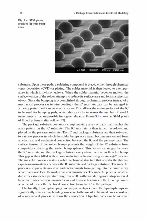
128 9 Package Construction and Electrical Modeling
Fig. 9.4 SEM photo-graph of flip-chip bumparray
substrate. Upon these pads, a soldering compound is placed either through chemicalvapor deposition (CVD) or plating. The solder material is then heated to a temper-ature in which it melts or reflows. When the solder material becomes molten, thesurface tension of the solder attempts to reduce its surface area and forms a sphericalobject. Since the bumping is accomplished through a chemical process instead of amechanical process (as in wire bonding), the IC substrate pads can be arranged inan array pattern and can be much smaller. This allows the entire surface of the ICto be used for bumping pads, which dramatically increases the number of level 1interconnects that are possible for a given die size. Figure 9.4 shows an SEM photoof flip-chip bumps after reflow [37].
The package substrate contains a complimentary array of pads that matches thearray pattern on the IC substrate. The IC substrate is then turned face-down andplaced on the package substrate. The IC and package substrates are then subjectedto a reflow process in which the solder bumps once again become molten and forman electrical and mechanical connection between the IC and the package pads. Thesurface tension of the solder bumps prevents the weight of the IC substrate fromcompletely collapsing the solder bump spheres. This leaves an air gap betweenthe IC substrate and the package substrate everywhere there is no flip-chip bump.This gap is then filled with a non-conductive adhesive using an underfill process.The underfill process creates a solid mechanical structure that absorbs the thermalexpansion mismatches between the IC substrate and package substrate. The underfillprocess also prevents moisture and contaminants from getting into the bump array,which can cause local thermal expansion mismatches. The underfill process is criticaldue to the extreme temperature range that an IC will cover during normal operation. Alarge thermal expansion mismatch can lead to stress fractures in the flip-chip bumpswhich could sever the electrical connection from the IC to the package.
Electrically, flip-chip bumping has many advantages. First, the flip-chip bumps aresignificantly smaller than bonding wires due to the use of a chemical process insteadof a mechanical process to form the connection. Flip-chip pads can be as small
9.2 Level 2 Interconnect 129
as 35 μm in diameter compared to 100 × 100 μm for a wire bond connection. Thereduced size of the interconnect leads to reduced parasitic inductance and capacitanceassociated with the connection. The lower electrical parasitics reduce all of the noisesources described in Sect. 8.2. The second electrical advantage of flip-chip bumpingis that the pads can be placed in an array pattern. This allows more pads to be placedfor a given substrate size compared to traditional perimeter placement used in wirebonding. The increased pad count leads to higher signal density and the possibility oflarge amounts of redundant power and ground connections. When redundant powerand ground paths are used it reduces the overall inductance in the power distributionpath. This results in less supply bounce (Eqs. 8.2 and 8.3).
The main disadvantage of flip-chip bumping is that it is more expensive than wirebonding. The cost is higher due to the manufacturing process that is required forflip-chip bumping. The bumping process must be carried out at the wafer level priorto individual IC separation. This means that ICs that have been identified as failuresduring electrical wafer test still receive the bumping process. As a result, more timeis associated with the process, which results in greater cost. In addition, the bumpingequipment must be able to accommodate the entire wafer instead of just the individualdie as in wire bonding. As wafer sizes continue to increase, the bumping equipmentmust be continually upgraded. These manufacturing factors have prevented the widespread adoption of flip-chip bumping despite its electrical advantages.
9.2 Level 2 Interconnect
The level 2 interconnect electrically connects the signals and power on the packageto the system PCB. The system PCB is constructed using a lamination process inwhich the outermost layers contain surface mount (SMT) pads, to which the packageis soldered. Since a lamination process is used, the pads on the PCB are muchlarger than that used in the level 1 connection. There are two main styles of level 2interconnect; lead frame and a ball grid array.
9.2.1 Lead Frame
A is a structure that forms the electrical and mechanical connection between thepackage and the system PCB. The lead frame begins as a single piece of copper-based alloy sheet metal that contains a die mounting paddle and lead fingers. Thefeatures of the lead frame are formed by stamping or etching, which is then followedby a plating finish to reduce oxidation. The die mounting paddle is used to support thedie during assembly. The lead fingers are used to form the connection to the systemPCB and extend outwards from the perimeter of the die paddle. Lead frames onlysupport wire bonding connections from the die. During assembly, the die resideson the die paddle while the wire bonding takes place to the outward extending leadfingers. The die paddle is then removed and the die is covered with a non-conductiveencapsulant that protects the IC substrate and helps dissipate heat. The lead fingers

130 9 Package Construction and Electrical Modeling
Fig. 9.5 Lead frameconnection to IC substrate
extend out of the encapsulant and are then trimmed and formed to their final shapeprior to mounting to the system PCB. At this point the leads can be shaped intothrough-hole or SMT connections. Figure 9.5 shows the wire bonding from the ICsubstrate to the fingers of a lead frame [37].
The lead frame assembly process has been refined over the past decades to yield aninexpensive solution to IC packaging; however, the lead frame suffers from the sameelectrical disadvantages as the wire bond in that the interconnect is relatively longwhich creates a large return current path. The large return current path increases theself-inductance of the lead and the mutual coupling capacitive between leads, bothof which increase package noise that limits the lead frame’s performance. Anotherdrawback of the lead frame is that it limits signal from the package to a perimeteregress. This limits the overall signal and power density that can be achieved by thisstyle of interconnect.
9.2.2 Array Pattern
To improve upon the lead frame package interconnect, packaging was introduced.BGA technology is very similar to flip-chip bumping except that the solder ballsreside between the package and the system PCB. Since the laminated constructionof the PCB limits the feature sizes that can be achieved, the density of the arraypattern that can be achieved is much less than flip-chip bumping. Current BGApackages range from 0.5 to 1.27 mm contact pitch [96]. Since the level 2 solder ballsare much larger than the flip-chip bumps, an underfill encapsulant is not needed since

9.3 Modern Packages 131
Fig. 9.6 SEM photo-graph of the bottom of a1 mm pitch BGA package
Fig. 9.7 Photograph of a1 mm pitch BGA package
the solder balls can absorb the majority of the thermal expansion mismatch betweenthe package and the system PCB. In addition, the BGA package substrate is typicallyimplemented using a PCB so the thermal expansion difference between the packageand the system PCB is minimized. As with the flip-chip bumping interconnect, theBGA interconnect reduces the overall parasitic inductance and capacitance in theinterconnect by reducing the electrical length relative to the lead frame approach.Also, the array configuration of the interconnect leads to the easy implementation ofredundant power and ground pins which decreases the self-inductance in the powersupply path. Figure 9.6 shows an SEM photograph of the underside of a 1 mm pitchBGA package [37].
Figure 9.7 shows a photograph of an entire BGA package highlighting the arrayconfiguration of the interconnect [37].
9.3 Modern Packages
This work will focus on three of the most common packages used in modern VLSIdesigns. These packages represent the past, present, and future technologies of ICpackaging and illustrate the electrical, mechanical, and cost trade-offs that have beenmade by VLSI designers.
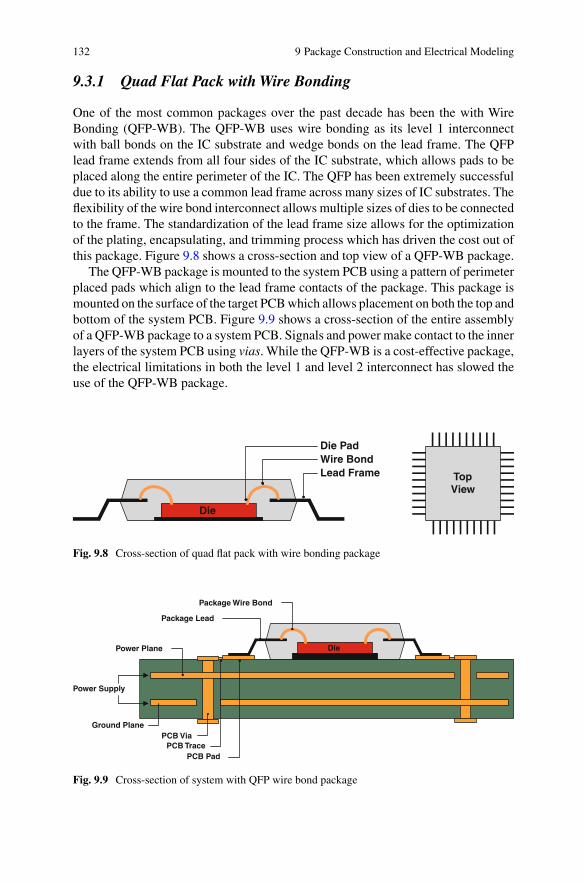
132 9 Package Construction and Electrical Modeling
9.3.1 Quad Flat Pack with Wire Bonding
One of the most common packages over the past decade has been the with WireBonding (QFP-WB). The QFP-WB uses wire bonding as its level 1 interconnectwith ball bonds on the IC substrate and wedge bonds on the lead frame. The QFPlead frame extends from all four sides of the IC substrate, which allows pads to beplaced along the entire perimeter of the IC. The QFP has been extremely successfuldue to its ability to use a common lead frame across many sizes of IC substrates. Theflexibility of the wire bond interconnect allows multiple sizes of dies to be connectedto the frame. The standardization of the lead frame size allows for the optimizationof the plating, encapsulating, and trimming process which has driven the cost out ofthis package. Figure 9.8 shows a cross-section and top view of a QFP-WB package.
The QFP-WB package is mounted to the system PCB using a pattern of perimeterplaced pads which align to the lead frame contacts of the package. This package ismounted on the surface of the target PCB which allows placement on both the top andbottom of the system PCB. Figure 9.9 shows a cross-section of the entire assemblyof a QFP-WB package to a system PCB. Signals and power make contact to the innerlayers of the system PCB using vias. While the QFP-WB is a cost-effective package,the electrical limitations in both the level 1 and level 2 interconnect has slowed theuse of the QFP-WB package.
TopView
Die
Die PadWire BondLead Frame
Fig. 9.8 Cross-section of quad flat pack with wire bonding package
Power Plane
Ground Plane
Package Wire Bond
PCB TracePCB Pad
Package Lead
Power Supply
Die
PCB Via
Fig. 9.9 Cross-section of system with QFP wire bond package
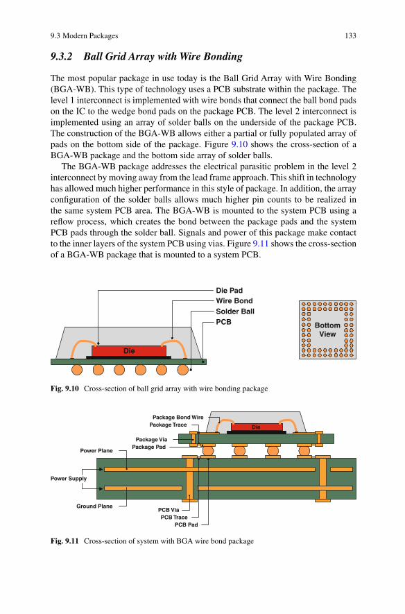
9.3 Modern Packages 133
9.3.2 Ball Grid Array with Wire Bonding
The most popular package in use today is the Ball Grid Array with Wire Bonding(BGA-WB). This type of technology uses a PCB substrate within the package. Thelevel 1 interconnect is implemented with wire bonds that connect the ball bond padson the IC to the wedge bond pads on the package PCB. The level 2 interconnect isimplemented using an array of solder balls on the underside of the package PCB.The construction of the BGA-WB allows either a partial or fully populated array ofpads on the bottom side of the package. Figure 9.10 shows the cross-section of aBGA-WB package and the bottom side array of solder balls.
The BGA-WB package addresses the electrical parasitic problem in the level 2interconnect by moving away from the lead frame approach. This shift in technologyhas allowed much higher performance in this style of package. In addition, the arrayconfiguration of the solder balls allows much higher pin counts to be realized inthe same system PCB area. The BGA-WB is mounted to the system PCB using areflow process, which creates the bond between the package pads and the systemPCB pads through the solder ball. Signals and power of this package make contactto the inner layers of the system PCB using vias. Figure 9.11 shows the cross-sectionof a BGA-WB package that is mounted to a system PCB.
BottomView
Die
Wire BondSolder BallPCB
Die Pad
Fig. 9.10 Cross-section of ball grid array with wire bonding package
Die
Power Plane
Ground PlanePCB Via
Package Via
Package Bond WirePackage Trace
PCB TracePCB Pad
Package Pad
Power Supply
Fig. 9.11 Cross-section of system with BGA wire bond package

134 9 Package Construction and Electrical Modeling
The BGA-WB has gained wide adoption due to its combination of the inex-pensive level 1 wire bonding interconnect with the advantages of an array stylelevel 2 interconnect. The main drawback of the BGA-WB is that it still suffersthe electrical parasitics associated with the level 1 wire bond interconnect. Thewire bond interconnect also restricts the pad placement on the IC to a perime-ter pattern which inherently limits the number of level 1 connections. This is themain limitation to the number of signals and power contacts that can be broughtout to the system PCB. Despite these disadvantages, the BGA wire bond is themost widely used package for current VLSI design starts due to its electrical ad-vantages over the QFP-WB and its cost-effectiveness relative to non-wire bondedpackages.
9.3.3 Ball Grid Array with Flip-Chip Bumping
The next step in the evolution of VLSI packaging is the Ball Grid Array with Flip-Chip bumping (BGA-FC). This package addresses the electrical parasitics of the wirebond by implementing flip-chip technology as its level 1 connection. When combinedwith the electrical improvements gained by using a level 2 BGA interconnect, theBGA-FC promises to meet the needs of VLSI systems into the next decade. Figure9.12 shows the cross-section of a BGA-FC package and the bottom side array ofsolder balls.
The BGA-FC package can achieve very high signal counts due to its array stylepad pattern. In a BGA-WB package the total number of interconnects is limitedby the wire bond noise that exists in the level 1 interconnect and the perimeter padplacement on the die. In the BGA-FC package this issue is addressed by implementingan array style interconnect between the IC and the package substrate. This allowshigher signal counts and redundant power and ground connections which reduces thepackage noise and increases system performance. Packages with up to 2000 contactshave been successfully implemented using ball grid array with flip-chip bumpingtechnology [40]. Figure 9.13 shows the cross-section of a BGA-FC package that ismounted to a system PCB.
BottomView
Die
Solder BallPCB
Die Pad
Fig. 9.12 Cross-section of ball grid array with flip-chip package

9.4 Electrical Modeling 135
Power Plane
Ground PlanePCB Via
Package Via
Flip-Chip Bump PadPackage Trace
PCB TracePCB Pad
Package Pad
Power Supply
Die
Flip-Chip Bump
Fig. 9.13 Cross-section of system with BGA flip-chip package
9.4 Electrical Modeling
This section presents the results of the electrical parameter extraction performed todetermine the inductance and capacitance magnitudes for the three packages studiedin this work. The three dimensional structures within the package were modeledand simulated using electromagnetic field solvers. A combination of Raphael fromAvant! [15] and Advanced Design System from Agilent Technologies, Inc [50] wereused to accomplish the parameter extraction.
9.4.1 Quad Flat Pack with Wire Bonding
The QFP-WB package studied in this work uses a 100-pin lead frame with 25 leadsper side on 0.8 mm pitch. The lead frame is composed of a copper based alloy witha tin plated finish. The IC is implemented on a 5 × 5 mm silicon die. The die isconnected to the lead frame with 25 μm diameter gold wire bonds. The bondingwires attach to the lead frame using wedge bonds onto 100 × 400 μm pads. The wireconnections to the IC are formed using ball bonds onto 100 × 100 μm pads. Thewire bonds range is length from 3 to 5 mm.
9.4.2 Ball Grid Array with Wire Bonding
The BGA-WB package studied in this work is a 20 × 20 array of 1 mm pitch,fully populated with solder balls. Each solder ball has an average diameter of 1 mmand an average collapsed height of 0.5 mm. The package substrate uses a 1.27 mmthick GETEK© substrate with traces designed for an impedance of 50 � using tracewidths of 0.1 mm. The wire bond connections to the package substrate are formed

136 9 Package Construction and Electrical Modeling
Table 9.1 Electrical parasitic magnitudes for studied packages
QFP-WB BGA-WB BGA-FC
L11 4.550 nH 3.766 nH 1.244 nHK12 0.744 0.537 0.330K13 0.477 0.169 0.287K14 0.352 0.123 0.230K15 0.283 0.097 0.200C0 300 fF 288 fF 197 fFC12 121 fF 115 fF 96 fFC13 17 fF 97 fF 9 fF
Table 9.2 Electrical parasitics for various wire bond lengths
Length (mm) Cwb(fF) Lwb(nH) Z0(�)
1 26 0.569 1482 52 1.138 1483 78 1.707 1484 104 2.276 1485 130 2.845 148
using 25 μm diameter gold wires to 100 × 400 μm wedge bond pads. The wireconnections to the IC are formed using ball bonds onto 100 × 100 μm pads. Thewire bonds range is length from 1 to 5 mm.
9.4.3 Ball Grid Array with Flip-Chip Bumping
The BGA-FC package studied in this work uses the same level 2 construction asthe BGA-WB described above. The level 1 interconnect is formed using a 100 ×100 array of flip-chip bumps that have an average diameter of 125 μm and averagecollapsed height of 75 μm. The flip-chip bumps connect complimentary arrays ofpads on the package substrate and on the IC. The pads on each substrate are 100 μmin diameter.
Table 9.1 lists the electrical parameter extraction results for the three packagesdescribed above. For each extraction the worst-case interconnect paths are extracted.These values represent the summation of all parasitic sources within the package.
The wire bond is the largest contributor of inductance in a bonded package. Thisinterconnect is the largest source of impedance discontinuity and, in turn, the largestsource of reflected noise. Chapter 15 presents an impedance compensation techniquefor this inductive interconnect so the specific electrical parasitics of a reasonablerange of wire bond lengths were also extracted. Table 9.2 lists the specific inductanceand capacitance parameters for a reasonable range of wire bond lengths used in theQFP-WB and BGA-WB packages.

Chapter 10Preliminaries and Terminology
10.1 Bus Construction
A bus is defined as a group of signals that transmits data from one circuit to another.When designing a bus that traverses a package, the number of physical interconnectpaths must be accounted for. This means that in addition to the total number ofsignal pins that are needed, the number of power and ground pins associated withthe bus must also be considered. In VLSI design there are typically an equal numberof power supply pins (VDD) as ground pins (VSS) [40, 59] for a given bus. For anarbitrarily large bus, individual bus segments can be defined that represent a subsetof signals within a bus that are associated with at least one VDD and at least one VSS
pin. By introducing the notation of a segment, subsets of the bus can be evaluatedfor performance instead of the entire bus, which leads to faster computation timeswithout any loss of electrical accuracy.
Definition 10.1 A bus segment consists of a group of contiguous signal pins, alongwith at least one VDD and at least one GND pin. The VDD (GND) pins are alsocontiguous in their placement.
In practice, buses are implemented in the form of concatenated segments, witheach segment having their VDD and GND pins on either side of the signal pins.
Definition 10.2 Let Nsegment represent the total number of pins within the segment.
Definition 10.3 Let Wbus represent the number of signal pins within an individualsegment.
Definition 10.4 Let Ng represent the number of VSS pins within the bus segmentwhere Ng ≥ 1.
Definition 10.5 Let Np represent the number of VDD pins within the bus segmentwhere Np ≥ 1.
This chapter describes the terminology and notation used throughout the rest of this monograph.
C. Duan et al., On and Off-Chip Crosstalk Avoidance in VLSI Design, 137DOI 10.1007/978-1-4419-0947-3_10, © Springer Science+Business Media LLC 2010

138 10 Preliminaries and Terminology
Fig. 10.1 Individual bussegment construction
VDD VSSS S S
segment
Wbus
Np = 1 Ng = 1
Figure 10.1 shows an example segment. In this segment there are three signal pins(Wbus = 3), one VSS pin (Ng = 1), and one VDD pin (Np = 1).
The ratio of signal-to-supply pins are defined to give a quick estimate of the qualityof the power and ground distribution is for a given bus segment.
Definition 10.6 The Signal-to-Power-Ground (SPG) metric is defined as Wbus : Np :Ng.
Definition 10.7 The Signal-to-Power-Ground Ratio (SPGR) is defined as Wbus/Np.It assumes that Np = Ng = 1.
In practice, most packages use Np = Ng = 1. For the example segment inFigure 10.1, SPG = 3 : 1 : 1 and SPGR = 3.
The segment representation above corresponds to the commonly practiced busconstruction in the VLSI industry today. We refer to segments by their index j, tokeep trace of the relative location of a segment with respect to others.
Definition 10.8 Suppose a given bus has k segments. We represent an arbitrarysegment of interest by its index j. Segments to the left of the jth segment are assignedindices j − 1, j − 2, . . . , j − (k/2). Segments to the right of the jth segment areassigned indices j + 1, j + 2, . . . , j + (k/2).
Definition 10.9 Let Nbus represent the total number of pin in an off-chip bus.
Nbus includes all signal, power, and ground pins that are used in the packageto construct the off-chip bus. Figure 10.2 shows an example bus construction thatconsists of 3 segments (k = 3). In this bus each segment has the same number ofsignal (Wbus = 3), power (Np = 1), and ground (Ng = 1) pins.
This notation allows a flexible framework that can represent arbitrarily largebusses. Further, this notation matches the practical implementation of buses in VLSI
VDD VSSS S S
Nbus
j-1 j j+1
VDD VSSS S S VDD VSSS S S
Fig. 10.2 Bus construction using multiple segments

10.2 Logic Values and Transitions 139
b3j-1b1
j-1
VDD VSSS S S
j-1 j j+1
VDD VSSS S S VDD VSSS S S
b0j b1
j b2j b3
j b4j b0
j+1 b1j+1 b2
j+1 b3j+1 b4
j+1b0j-1 b2
j-1 b4j-1
Fig. 10.3 Pin representation in a bus
designs. The number of pins within a segment is shown in Eq. 10.1.
Nsegment = Wbus + Np + Ng (10.1)
The number of a pins within the entire bus is defined in Eq. 10.2.
Nbus = Nsegment · k (10.2)
In order to specify the exact location within a bus and/or segment, an individual pinnotation is defined. Each pin within a bus segment is given the notation b. Within agiven segment, i is defined as the relative pin location.
Definition 10.10 The ith pin of the jth segment is denoted bji . The indices i and j
start with 0 and increase from left to right.
This framework allows the spatial location of any pin bji within a bus to be de-
scribed. Figure 10.3 shows an example bus using the spatial pin notation bji . The
arithmetic in the subscript of bji is performed modulo Nsegment. This allows a con-
sistent method to describe relative locations of pins across segment boundaries. Forexample, if Nsegment = 5, then bj
2 = bj−12+5 = bj+1
2−5.
10.2 Logic Values and Transitions
Definition 10.11 sji represents the logic state of pin bj
i . For a signal pin, sji can take
on a value of 0 or 1 which represents the Boolean logic value for pin bji . For a VSS
pin, sji = 0, and for a VDD pin, sj
i = 1.
Definition 10.12 vji represents the transition on any pin bj
i . vji = 0 when no tran-
sition occurs on pin bji . vj
i = 1 when pin bji transitions from a logic 0 to a logic 1.
vji = −1 when pin bj
i transitions from a logic 1 to a logic 0. vji = 0 for VSS or
VDD pins.
Figure 10.4 shows an example bus, illustrating the notation for the state andtransition of each pin.
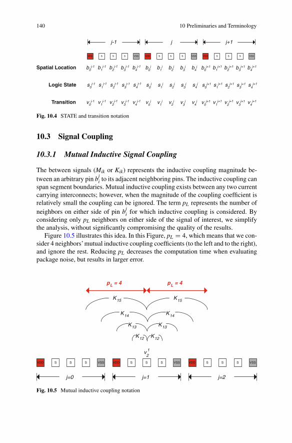
140 10 Preliminaries and Terminology
VDD VSSS S S
j-1 j j+1
VDD VSSS S S VDD VSSS S S
s0j s1
j s2j s3
j s4j s0
j+1 s1j+1 s2
j+1 s3j+1 s4
j+1s0j-1 s1
j-1 s2j-1 s3
j-1 s4j-1
b3j-1b1
j-1 b0j b1
j b2j b3
j b4j b0
j+1 b1j+1 b2
j+1 b3j+1 b4
j+1b0j-1 b2
j-1 b4j-1
v0j v1
j v2j v3
j v4j v0
j+1 v1j+1 v2
j+1 v3j+1 v4
j+1v0j-1 v1
j-1 v2j-1 v3
j-1 v4j-1
Spatial Location
Logic State
Transition
Fig. 10.4 STATE and transition notation
10.3 Signal Coupling
10.3.1 Mutual Inductive Signal Coupling
The between signals (Mik or Kik) represents the inductive coupling magnitude be-tween an arbitrary pin bj
i to its adjacent neighboring pins. The inductive coupling canspan segment boundaries. Mutual inductive coupling exists between any two currentcarrying interconnects; however, when the magnitude of the coupling coefficient isrelatively small the coupling can be ignored. The term pL represents the number ofneighbors on either side of pin bj
i for which inductive coupling is considered. Byconsidering only pL neighbors on either side of the signal of interest, we simplifythe analysis, without significantly compromising the quality of the results.
Figure 10.5 illustrates this idea. In this Figure, pL = 4, which means that we con-sider 4 neighbors’mutual inductive coupling coefficients (to the left and to the right),and ignore the rest. Reducing pL decreases the computation time when evaluatingpackage noise, but results in larger error.
VDD
j=0 j=1 j=2
VDD VDDVSS VSSVSSS S S S S S S S S
v21
K12 K12
K13 K13
K14 K14
K15 K15
pL = 4 pL = 4
Fig. 10.5 Mutual inductive coupling notation
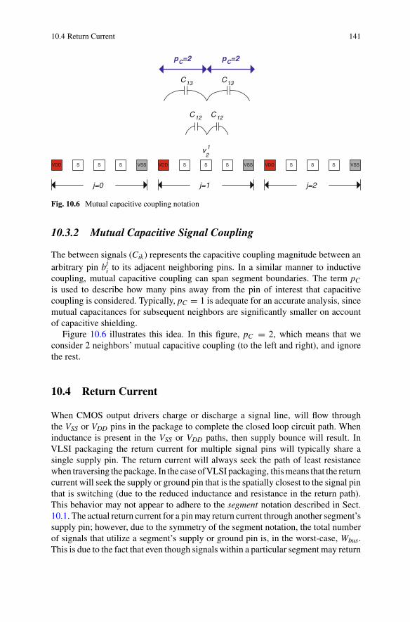
10.4 Return Current 141
VDD
j=0 j=1 j=2
VDD VDDVSS VSSVSSS S S S S S S S S
v21
C12 C12
pC=2
C13 C13
pC=2
Fig. 10.6 Mutual capacitive coupling notation
10.3.2 Mutual Capacitive Signal Coupling
The between signals (Cik) represents the capacitive coupling magnitude between anarbitrary pin bj
i to its adjacent neighboring pins. In a similar manner to inductivecoupling, mutual capacitive coupling can span segment boundaries. The term pC
is used to describe how many pins away from the pin of interest that capacitivecoupling is considered. Typically, pC = 1 is adequate for an accurate analysis, sincemutual capacitances for subsequent neighbors are significantly smaller on accountof capacitive shielding.
Figure 10.6 illustrates this idea. In this figure, pC = 2, which means that weconsider 2 neighbors’ mutual capacitive coupling (to the left and right), and ignorethe rest.
10.4 Return Current
When CMOS output drivers charge or discharge a signal line, will flow throughthe VSS or VDD pins in the package to complete the closed loop circuit path. Wheninductance is present in the VSS or VDD paths, then supply bounce will result. InVLSI packaging the return current for multiple signal pins will typically share asingle supply pin. The return current will always seek the path of least resistancewhen traversing the package. In the case ofVLSI packaging, this means that the returncurrent will seek the supply or ground pin that is the spatially closest to the signal pinthat is switching (due to the reduced inductance and resistance in the return path).This behavior may not appear to adhere to the segment notation described in Sect.10.1. The actual return current for a pin may return current through another segment’ssupply pin; however, due to the symmetry of the segment notation, the total numberof signals that utilize a segment’s supply or ground pin is, in the worst-case, Wbus.This is due to the fact that even though signals within a particular segment may return

142 10 Preliminaries and Terminology
VDD VSSS S S
j-1 j j+1
VDD VSSS S S VDD VSSS S S
I3j-1I1
j-1 I1j I2
j I3j I1
j+1 I2j+1 I3
j+1I2j-1
(Wbus) (Wbus) (Wbus)
Fig. 10.7 Return current description
current through an adjacent segment’s supply pin (which is spatially closer), signalsfrom adjacent segments will return current through the supply pins of the segment ofinterest (because its supply pin is spatially closer to those signals). This allows theevaluation of an individual segment for supply bounce, considering only the signalpins within that segment. This does not lead to a reduction in modeling accuracy.This results in a much simpler analytical model for bus performance modeling andnoise evaluation.
Figure 10.7 shows how the return current for a signal can span segment boundariesyet the total amount of return current within a segment will always be Wbus · I . Weassume that all the currents Ij
i are identical, and equal to I .
10.5 Noise Limits
The maximum allowable noise for any of the noise sources described in Sect. 8.2 isexpressed in terms of user-defined parameters. For supply bounce, signal coupling,and reflected voltage, the noise limits are expressed as a percentage of VDD. Px ·VDD
is the maximum allowable voltage noise defined by the user, where 0 ≤ Px ≤ 1.Figure 10.8 shows how the user-defined noise limits are expressed in terms of VDD.
Fig. 10.8 Package noisenotation
Vnoise
v(t)VDD
Px * VDD
t

10.5 Noise Limits 143
Definition 10.13 Pgnd represent the maximum allowable amount of ground bouncein the system. Pgnd is defined as a fraction of VDD such that the noise due to groundbounce is ≤ Pgnd · VDD.
Definition 10.14 N−1 represent the number of signal pins within a segment that aretransitioning from a logic 1 to a logic 0. This number represents the number of signalsthat are returning current through the VSS pin and resulting in ground bounce.
Definition 10.15 Psupply represent the maximum allowable amount of supply bouncein the system. Psupply is defined as a fraction of VDD such that the noise due to supplybounce is ≤ Psupply · VDD.
Definition 10.16 N1 represent the number of signal pins within a segment that aretransitioning from a logic 0 to a logic 1. This number represents the number of signalsthat are drawing current through the VDD pin and resulting in supply bounce.
Definition 10.17 P0 represent the maximum allowable amount of glitching noisein the system. P0 is defined as a fraction of VDD such that the absolute value of theglitching noise is ≤ P0 · VDD.
A glitch occurs when a victim signal is static while neighboring signals transitioncausing mutual inductive and capacitive coupling onto the victim line.
Definition 10.18 P1 represent the maximum allowable amount of rising edge cou-pling noise in the system. P1 is defined as a fraction of VDD such that the rising edgecoupling noise due to all neighboring signals is ≤ P1 · VDD.
Rising edge coupling occurs when a victim signal is transitioning from a logic 0to a logic 1 at the same time that neighboring signals are transitioning and causingmutual inductive and capacitive coupling onto the victim line. This coupling caneither speed up, slow down, or leave unaffected the rising edge on the victim line.
Definition 10.19 P−1 represent the maximum allowable amount of falling edgecoupling noise in the system. P−1 is defined as a fraction of VDD such that the fallingedge coupling noise due to all neighboring signals is ≤ P−1 · VDD.
Falling edge coupling occurs when a victim signal is transitioning from a logic 1to a logic 0 at the same time that neighboring signals are transitioning and causingmutual inductive and capacitive coupling onto the victim line. This coupling caneither speed up, slow down, or leave unaffected the falling edge on the victim line.
Definition 10.20 P� represent the maximum allowable amount of reflected noise inthe system. P� is defined as a fraction of VDD such that the absolute value of thereflected noise is ≤ P� · VDD.
When expressing the noise limit for capacitive bandwidth limiting, it is not ap-plicable to use a fraction of VDD; instead, the fraction by which the risetime of thesignal is increased due to switching neighboring pins is used.
Definition 10.21 PBW represent the maximum amount that the original risetime ofa signal is altered due to switching neighboring pins. The original risetime is defined

144 10 Preliminaries and Terminology
Fig. 10.9 Bandwidthlimitation notation
v(t) (0.8)*VDD
t
improvement
original
degradation
10%
90%
as the time it takes to switch from 10% of VDD to 90% of VDD while all other signalpins are held at a logic 0.
When neighboring signal pins switch they change the effective capacitance thatthe victim signal experiences. This can cause the victim signal risetime to speedup, slow down, or remain the same. The fraction of risetime alteration is positivewhen the original risetime is sped up due to neighboring signal pins that switch. Thefraction of risetime alteration is negative when the original risetime is slowed downdue to neighboring signal pins that switch. Equation 10.3 gives the expression forhow PBW is defined. Figure 10.9 illustrates the mechanism of bandwidth limitingand how it relates to PBW.
PBW = torig − tnew
torig(10.3)

Chapter 11Analytical Model for Off-ChipBus Performance
The noise sources described in Sect. 8.2 limit the maximum performance that an off-chip bus can achieve. This occurs because the package noise sources are proportionalto the rate of change in current or voltage ( di
dt and dvdt ). When any given noise source
exceeds the user-defined limits described in Sect. 10.5, the rate of change of currentor voltage must be reduced.
11.1 Package Performance Metrics
The performance of an off-chip bus depends on how fast the digital output driverscan switch the output voltage levels. This relates to how much data that one pin ofthe bus can transmit per second. The term Unit Interval (UI) represents the shortestamount of time that data can be present on an individual pin and still accuratelytransmit the logic value from the Transmitter (Tx) to the Receiver (Rx) in the off-chip bus. The UI of a pin is directly related to the maximum switching speed that thesystem can achieve. Figure 11.1 shows a graphical representation of the Unit Intervalmetric.
The minimum can be translated into the maximum Datarate (DR) of an individualpin using Eq. 11.1.
DRmax = 1
UImin(11.1)
Since the off-chip bus segment is constructed using multiple signal pins, the maxi-mum Throughput (TP) of the bus segment can be found using Eq. 11.2. Figure 11.2shows a graphical representation of throughput.
TPmax = DRmax · Wbus (11.2)
C. Duan et al., On and Off-Chip Crosstalk Avoidance in VLSI Design, 145DOI 10.1007/978-1-4419-0947-3_11, © Springer Science+Business Media LLC 2010
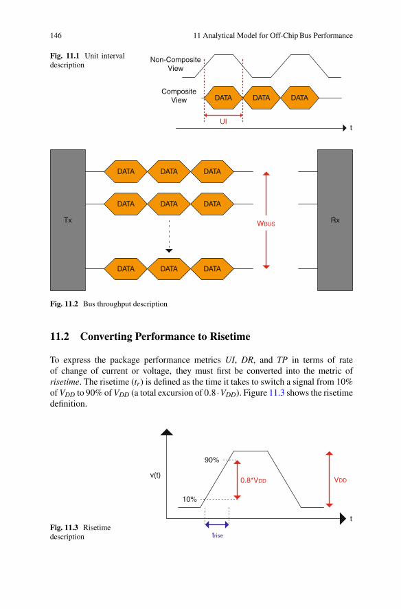
146 11 Analytical Model for Off-Chip Bus Performance
Fig. 11.1 Unit intervaldescription
DATA
t
DATA DATA
UI
Non-CompositeView
CompositeView
DATA DATA DATA
DATA DATA DATA
DATA DATA DATA
WBUSRxTx
Fig. 11.2 Bus throughput description
11.2 Converting Performance to Risetime
To express the package performance metrics UI, DR, and TP in terms of rateof change of current or voltage, they must first be converted into the metric ofrisetime. The risetime (tr) is defined as the time it takes to switch a signal from 10%of VDD to 90% of VDD (a total excursion of 0.8 ·VDD). Figure 11.3 shows the risetimedefinition.
Fig. 11.3 Risetimedescription
v(t)VDD
t
10%
90%
0.8*VDD
trise

11.3 Converting Bus Performance to didt and dv
dt 147
Fig. 11.4 Risetime to unitinterval conversion
DATA
UI
trise
1.5*trise
Non-CompositeView
CompositeView
When a digital signal switches, the signal must be given adequate time to reachits steady state value before the next switching event occurs. The amount of timethat is required is UImin and can be expressed in terms of risetime (Eq. 11.3). Fora robust digital system, the Unit Interval must be greater than or equal to 1.5 timesthe risetime [32, 58]. Figure 11.4 shows the graphical representation of how risetimerelates to the minimum Unit Interval.
UImin = 1.5 · trise (11.3)
11.3 Converting Bus Performance to didt and dv
dt
Once the package performance has been expressed in terms of risetime, it can thenbe converted into the rate of change of current or voltage. The first step is to convertrisetime into slewrate. Slewrate is defined as the rate of change in voltage ( dv
dt )and typically is expressed in the units of V
ns . Slewrate can also be converted to thecorresponding di
dt by dividing it by the characteristic impedance of the system inwhich the package resides. Equation 11.4 expresses slewrate in terms of the rateof change in current or voltage. Figure 11.5 shows a graphical representation ofslewrate.
slewrate = dv
dt= di
dt· Z0 (11.4)
Fig. 11.5 Slewratedescription
v(t) VDD
t
dt
dv

148 11 Analytical Model for Off-Chip Bus Performance
Using the definition of risetime as the time taken to switch from 10% of VDD to 90%of VDD (an excursion of 0.8 · VDD), risetime can be expressed in terms of slewrateby Eq. 11.5.
trise = 0.8 · VDD
slewrate(11.5)
This, in turn, can be converted to a relationship between the package performanceand the rate of change of current or voltage using Eqs. 11.6 and 11.7.
DRmax =
(dv
dt
)
(1.5) · (0.8) · (VDD)=
(di
dt
)· Z0
(1.5) · (0.8) · (VDD)(11.6)
TPmax =
(dv
dt
)· Wbus
(1.5) · (0.8) · (VDD)=
(di
dt
)· Z0 · Wbus
(1.5) · (0.8) · (VDD)(11.7)
11.4 Translating Noise Limits to Performance
Now that the noise sources described in Sect. 8.2 and the package performancemetrics in Sect. 11.1 have been expressed in terms of the rate of change in currentor voltage, a relationship between the noise limits and package performance can beconstructed. For each noise source, the maximum datarate and throughput is foundthat does not violate any user-defined noise limit parameter. The noise source thatapproaches its user-defined limit first is the limiting source to performance.
11.4.1 Inductive Supply Bounce
When considering the performance limitation due to inductive supply bounce thefastest rate of di
dt is found that results in the user-defined noise limits Psupply or Pgnd
being violated. The first step is to find an expression for the total amount of supplybounce that results as a consequence of signal switching. The total amount of supplybounce is evaluated over one bus segment. The evaluation must include all signalswithin the bus segment (Wbus) that return current through the supply pin inductance(L11). In addition, any mutual inductive and capacitive signal coupling onto thesupply pin must be accounted for. Supply bounce and mutual inductive coupling arealready in terms of di
dt ; however, mutual capacitive coupling must first be convertedinto an expression that considers the rate of change of current or voltage. In order todo this, Eq. 8.9 is modified to include how the forcing function (trise) interacts withthe natural response (τRC) of the capacitively coupled circuit [21, 32]. Performing theinverse Laplace Transform on an exponential ramp forcing function and assumingan RC natural response, the capacitive voltage divider is multiplied by (τRC/trise)
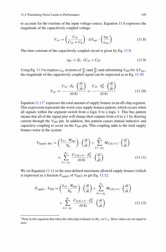
11.4 Translating Noise Limits to Performance 149
to account for the risetime of the input voltage source. Equation 11.8 expresses themagnitude of the capacitively coupled voltage.
Vvic =(
C1k
C1k + C0
)· �Vagr ·
(τRC
trise
)(11.8)
The time constant of the capacitively coupled circuit is given by Eq. 11.9.
τRC = Z0 · (C1k + C0) (11.9)
Using Eq. 11.5 to express trise in terms of dvdt (and di
dt ) and substituting VDD for �Vagr ,the magnitude of the capacitively coupled signal can be expressed as in Eq. 11.10.
Vvic =C1k · Z0 ·
(dv
dt
)
(0.8)=
C1k · Z20 ·(
di
dt
)
(0.8)(11.10)
Equation 11.111 expresses the total amount of supply bounce in an off-chip segment.This expression represents the worst-case supply bounce pattern, which occurs whenall signals within the segment switch from a logic 0 to a logic 1. This bus patternmeans that all of the signal pins will charge their outputs from a 0 to a 1 by drawingcurrent through the VDD pin. In addition, this pattern causes mutual inductive andcapacitive coupling to occur on the VDD pin. This coupling adds to the total supplybounce noise in the system.
VSupply–Bnc =(
L11 · Wbus
Np
)·(
di
dt
)+
pL∑
k=−pL
M1(|k|+1) ·(
di
dt
)
+pC∑
k=−pC
C1(|k|+1) · Z20
(0.8)·(
di
dt
)(11.11)
We set Equation 11.11 to the user-defined maximum allowed supply bounce (whichis expressed as a fraction Psupply of VDD), to get Eq. 11.12.
Psupply · VDD =(
L11 · Wbus
Np
)·(
di
dt
)+
pL∑
k=−pL
M1(|k|+1) ·(
di
dt
)
+pC∑
k=−pC
C1(|k|+1) · Z20
(0.8)·(
di
dt
)(11.12)
1Note in this equation that when the subscript evaluates to M11 or C11, these values are set equal tozero.

150 11 Analytical Model for Off-Chip Bus Performance
By factoring didt out of Eq. 11.12 and substituting into Eq. 11.6, the maximum datarate
that can be achieved without violating the user-defined noise limit for supply bouncecan be found (Eq. 11.13).
DRmax−supply = Psupply · Z0
(1.5) · (0.8) ·[(
L11 · Wbus
Np
)+∑pL−pL
M1(|k|+1) +∑pC−pC
C1(|k|+1) · Z20
(0.8)
]
(11.13)
This, in turn, can be translated into the maximum throughput of the segment bymultiplying it by the number of signals within the segment (Eq. 11.14).
TPmax−supply = Psupply · Z0 · Wbus
(1.5) · (0.8) ·[(
L11 · Wbus
Np
)+∑pL−pL
M1(|k|+1) +∑pC−pC
C1(|k|+1) · Z20
(0.8)
]
(11.14)
In a similar manner, the maximum datarate and throughput for a system (such thatthe user-defined noise limit Pgnd is not violated) can be derived. These expressionsare given in Eqs. 11.15 and 11.16.
DRmax−gnd = Pgnd · Z0
(1.5) · (0.8) ·[(
L11 · Wbus
Ng
)+∑pL−pL
M1(|k|+1) +∑pC−pC
C1(|k|+1) · Z20
(0.8)
]
(11.15)
TPmax−gnd = Pgnd · Z0 · Wbus
(1.5) · (0.8) ·[(
L11 · Wbus
Ng
)+∑pL−pL
M1(|k|+1) +∑pC−pC
C1(|k|+1) · Z20
(0.8)
]
(11.16)
11.4.2 Capacitive Bandwidth Limiting
When considering the in the package, the slowest RC time constant is found whichcorresponds to the worst-case switching pattern on the bus. This time constant is thentranslated into risetime, which in turn is translated into datarate and throughput asin the previous section. For capacitive bandwidth limitation, the worst-case patternon the bus occurs when the center pin within the segment transitions from a logic0 to a 1 while all other signals switch from a 1 to a 0 (or vice versa). This switch-ing pattern results in the highest effective capacitance on the victim signal. Thiscapacitance will result in the slowest risetime since it results in the largest RC timeconstant for the bus segment. This dictates the maximum datarate and throughputthat can be achieved in the package. Combining Eqs. 8.7 and 8.8 gives the maximum

11.4 Translating Noise Limits to Performance 151
risetime that a given package can achieve when considering capacitive bandwidthlimitation.
trise−BW = 2.2 · Z0 ·⎛
⎝C0 +pC∑
k=−pC
2 · C1(|k|+1)
⎞
⎠ (11.17)
This can be directly converted to datarate and throughput using Eq. 11.3. Equations11.18 and 11.19 give the expressions for the maximum datarate and throughput thata package can achieve when considering bandwidth limitation.
DRmax−BW = 1
(1.5) · (2.2) · Z0 · (C0 +∑pC−pC2 · C1(|k|+1))
(11.18)
TPmax−BW = Wbus
(1.5) · (2.2) · Z0 · (C0 +∑pC−pC2 · C1(|k|+1))
(11.19)
11.4.3 Signal Coupling
The derivation of the magnitude is performed exactly as in Sect. 11.4.1. Equation11.20 expresses the maximum amount of noise voltage due to mutually inductive andcapacitive signal coupling onto a victim line. This expression describes the couplednoise when the victim signal is either static (P0), rising (P1), or falling (P−1).
Vcoupling =pL∑
k=−pL
M1(|k|+1) ·(
di
dt
)+
pC∑
k=−pC
C1(|k|+1) · Z20
(0.8)·(
di
dt
)(11.20)
Equating this to the user-defined maximum allowed coupled noise (which is ex-pressed as a fraction P0, P1, or P−1 of VDD), we get Eq. 11.21.
P(0/−1/1) · VDD =pL∑
k=−pL
M1(|k|+1) ·(
di
dt
)+
pC∑
k=−pC
C1(|k|+1) · Z20
(0.8)·(
di
dt
)(11.21)
By factoring didt out of Eq. 11.21 and substituting into Eq. 11.6, the maximum datarate
that can be achieved without violating the user-defined noise limits for signal couplingcan be found (Eq. 11.22).
DRmax−coupling = P(0/−1/1) · Z0
(1.5) · (0.8) ·[∑pL−pL
M1(|k|+1) +∑pC−pC
C1(|k|+1) · Z20
(0.8)
]
(11.22)

152 11 Analytical Model for Off-Chip Bus Performance
Equation 11.23 expresses the maximum throughput when considering the user-defined noise limits for signal coupling.
TPmax−coupling = P(0/−1/1) · Z0 · Wbus
(1.5) · (0.8) ·[∑pL−pL
M1(|k|+1) +∑pC−pC
C1(|k|+1) · Z20
(0.8)
]
(11.23)
11.4.4 Impedance Discontinuities
When evaluating a package for transmission line reflections due to, the forcing func-tion and natural response of the circuit must be considered in the evaluation of Eqs.8.13 and 8.14. To accomplish this we assume that the natural response of the packagebehaves as a low-pass RC filter. This allows the same derivations made in Sect. 11.4.1to be applied to the evaluation of the transmission line reflections. Equation 11.24expresses the magnitude of the reflection, considering the forcing function and thenatural response of the package.
Vreflected = Vincident · (�) ·(
τRC
trise
)(11.24)
Substituting the RC time constant given in Equation 11.9 and replacing Vincident withVDD, the reflected voltage can be expressed in terms of the user-defined noise limit(which is expressed as a fraction P� of VDD).
P� · VDD = VDD · (�) ·(
Z0 · (∑pC−pCC1(|k|+1) + C0
)
trise
)(11.25)
This can be substituted into Eq. 11.6 to find the maximum datarate that does notviolate the user-defined noise limit P� . Equations 11.26 and 11.27 give the datarateand throughput when considering the maximum allowable noise due to impedancediscontinuities.
DRmax−� = P�
(1.5) · � · Z0 · (∑pC−pCC1(|k|+1) + C0
) (11.26)
TPmax−� = P� · Wbus
(1.5) · � · Z0 · (∑pC−pCC1(|k|+1) + C0
) (11.27)
11.5 Experimental Results
In order to verify the analytical model, SPICE [76] simulations were performed ona test circuit. The test circuit includes a model for the package parasitics describedin Table 9.1. The test circuit is used to monitor noise limit violations due to thepackage as the performance of the output driver is increased. By monitoring noiselimit violations the simulation can indicate the maximum datarate and throughput for

11.5 Experimental Results 153
a given package and bus configuration. These simulation results are compared to theanalytical model predictions to verify the model’s accuracy.
11.5.1 Test Circuit
The test circuit used in this analysis consists of a standard CMOS inverter as the outputdriver. The CMOS inverter is implemented using the BPTM 0.1 μm [1] technologyusing BSIM3 model cards [2]. The CMOS inverter is sized to have an equal drivestrength when outputting a logic 0 or a logic 1 by sizing the PMOS and NMOStransistors such that ( WP
WN) = ( un
up) = 3.25 [59]. The CMOS inverter drives through the
Tx package model onto a PCB. The PCB contains a series termination resistor (Rs)followed by 2′′ of 50 � transmission line. The receiver load is modeled using theinput to a CMOS inverter that is sized to have a gate capacitance of 3 pF. A packagemodel is also inserted in the signal and power path prior to the Rx inverter. Boththe Tx and Rx inverters have VDD = 1.5 v and VSS = 0 v. The output risetime ofthe transmitter is altered by resizing the CMOS transistors in the inverter. Increasingthe size of the transistor will result in a smaller risetime. Figure 11.6 shows the testcircuit topology.
For each of the three packages studied in this work (QFP-WB, BGA-WB, andBGA-FC), the number of switching signal pins within a segment are varied fromWbus = 1 to Wbus = 16 in the simulation. In addition, three different SPG con-figurations are used to observe the effect of adding power and ground pins to thesegment. The three SPG configurations used are SPG = 8 : 1 : 1, SPG = 4 : 1 : 1,and SPG = 2 : 1 : 1. The user-defined noise limits are set to 5% of VDD so that
D(0)
D(1)
PackageModel
PCB
RS
RS
PCB
PackageModel
VDD Internal(Rx)
VDD Internal(Tx)
VSS Internal(Rx)
VSS Internal(Tx)
+1.5 v
Gnd
Fig. 11.6 Test circuit used to verify analytical model

154 11 Analytical Model for Off-Chip Bus Performance
Psupply = Pgnd = P0 = P1 = P−1 = −PBW = P� = 0.05. It was found that for thethree packages studied, supply bounce (Psupply, Pgnd) was always the limiting factorto performance.
11.5.2 Quad Flat Pack with Wire Bonding Results
Figure 11.7 shows the per-pin datarate for the QFP-WB package as a function ofthe number of signal pins within the segment. This plot shows the predicted dataratefor the analytical model versus the simulated results. These results illustrate thatthe per-pin datarate needs to be reduced as channels are added to the bus segment inorder to keep the noise below the user-defined limits. This plot also shows the amountof ground and power pins per segment influences the performance of the segment.Segments with a lower SPR perform at higher datarates due to the reduction in thetotal di
dt that is drawn through each supply pin.Figure 11.8 shows the bus throughput for the QFP-WB package as a function of the
number of signals pins within the segment. Due to the reduction in per-pin datarateas channels are added to the segment, throughput does not increase linearly with theaddition of channels; instead, the throughput follows a less than linear increase aspins are added to the segment.
Figure 11.9 shows the error percentage between the simulation results and ana-lytical model prediction for each size of segment evaluated in the QFP-WB package.
0
200
400
600
800
1000
1200
1400
1600
1800
2000
0 2 4 6 8 10 12 14 16(# of Channels)
(Mb
/s)
QFP-WB, 8:1:1 SPG (Sim)QFP-WB, 8:1:1 SPG (Mod)QFP-WB, 4:1:1 SPG (Sim)QFP-WB, 4:1:1 SPG (Mod)QFP-WB, 2:1:1 SPG (Sim)QFP-WB, 2:1:1 SPG (Mod)
Fig. 11.7 Per-Pin datarate for a QFP-WB package

0
300
600
900
1200
1500
1800
2100
2400
2700
3000
0 2 4 6 8 10 12 14 16(# of Channels)
(Mb
/s)
QFP-WB, 8:1:1 SPG (Sim)QFP-WB, 8:1:1 SPG (Mod)QFP-WB, 4:1:1 SPG (Sim)QFP-WB, 4:1:1 SPG (Mod)QFP-WB, 2:1:1 SPG (Sim)QFP-WB, 2:1:1 SPG (Mod)
Fig. 11.8 Throughput for a QFP-WB package
0
5
10
15
20
25
30
35
40
45
50
0 2 4 6 8 10 12 14 16(# of Channels)
(Err
or
%)
QFP-WB, 8:1:1 SPGQFP-WB, 4:1:1 SPGQFP-WB, 2:1:1 SPG
Fig. 11.9 Model accuracy for a QFP-WB package

156 11 Analytical Model for Off-Chip Bus Performance
This plot illustrates the accuracy of the analytical model. In almost all cases theaccuracy of the model is within 10% of the simulated results. The analytical modelexhibits the largest error for a bus size of 1 channel due to the higher frequencycomponents being present in the forcing function; however, even with an error of23% for 1 channel, the correlation of the analytical model is still within an acceptablerange.
11.5.3 Ball Grid Array with Wire Bonding Results
Figure 11.10 shows the per-pin datarate results for the BGA-WB package. This figureillustrates how the reduction in the electrical parasitics of the level 2 interconnecttranslates into increased performance. By moving to the BGA-WB package withless electrical parasitics, the per-pin datarate is increased as much as 25% over theQFP-WB. As with the results for the QFP-WB, performance is also increased byusing a lower SPG Ratio. Also, the per-pin datarate decreases with more switchingchannels as was observed for the QFP-WB package, for the same reasons.
Figure 11.11 shows the throughput for the BGA-WB package. Again, the through-put experiences a less than linear increase in performance as channels are added tothe bus segment. In addition, the throughput suffers a plateau at low channel counts
0
250
500
750
1000
1250
1500
1750
2000
2250
2500
100 2 4 6 8 12 14 16(# of Channels)
(Mb
/s)
BGA-WB, 8:1:1 SPG (Sim)BGA-WB, 8:1:1 SPG (Mod)BGA-WB, 4:1:1 SPG (Sim)BGA-WB, 4:1:1 SPG (Mod)BGA-WB, 2:1:1 SPG (Sim)BGA-WB, 2:1:1 SPG (Mod)
Fig. 11.10 Per-Pin datarate for a BGA-WB package
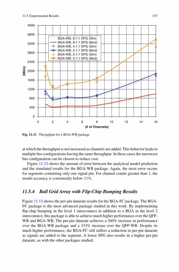
11.5 Experimental Results 157
0
400
800
1200
1600
2000
2400
2800
3200
3600
4000
1086420 12 14 16
(# of Channels)
(Mb
/s)
BGA-WB, 8:1:1 SPG (Sim)BGA-WB, 8:1:1 SPG (Mod)BGA-WB, 4:1:1 SPG (Sim)BGA-WB, 4:1:1 SPG (Mod)BGA-WB, 2:1:1 SPG (Sim)BGA-WB, 2:1:1 SPG (Mod)
Fig. 11.11 Throughput for a BGA-WB package
at which the throughput is not increased as channels are added. This behavior leads tomultiple bus configurations having the same throughput. In these cases the narrowestbus configuration can be chosen to reduce cost.
Figure 11.12 shows the amount of error between the analytical model predictionand the simulated results for the BGA-WB package. Again, the most error occursfor segments containing only one signal pin. For channel counts greater than 1, themodel accuracy is consistently below 11%.
11.5.4 Ball Grid Array with Flip-Chip Bumping Results
Figure 11.13 shows the per-pin datarate results for the BGA-FC package. The BGA-FC package is the most advanced package studied in this work. By implementingflip-chip bumping in the level 1 interconnect in addition to a BGA in the level 2interconnect, this package is able to achieve much higher performance over the QFP-WB and BGA-WB. The per-pin datarate achieves a 260% increase in performanceover the BGA-WB package and a 333% increase over the QFP-WB. Despite itsmuch higher performance, the BGA-FC still suffers a reduction in per-pin datarateas signals are added to the segment. A lower SPG also results in a higher per-pindatarate, as with the other packages studied.

0
5
10
15
20
25
30
35
40
45
50
0 2 4 6 8 10 12 14 16(# of Channels)
(Err
or
%)
BGA-WB, 8:1:1 SPGBGA-WB, 4:1:1 SPGBGA-WB, 2:1:1 SPG
Fig. 11.12 Model accuracy for a BGA-WB package
0
600
1200
1800
2400
3000
3600
4200
4800
5400
6000
100 2 4 6 8 12 14 16
(# of Channels)
(Mb
/s)
BGA-FC, 8:1:1 SPG (Sim)BGA-FC, 8:1:1 SPG (Mod)BGA-FC, 4:1:1 SPG (Sim)BGA-FC, 4:1:1 SPG (Mod)BGA-FC, 2:1:1 SPG (Sim)BGA-FC, 2:1:1 SPG (Mod)
Fig. 11.13 Per-Pin datarate for a BGA-FC package

11.5 Experimental Results 159
0
1000
2000
3000
4000
5000
6000
7000
8000
9000
10000
100 2 4 6 8 12 14 16(# of Channels)
(Mb
/s)
BGA-FC, 8:1:1 SPG (Sim)BGA-FC, 8:1:1 SPG (Mod)BGA-FC, 4:1:1 SPG (Sim)BGA-FC, 4:1:1 SPG (Mod)BGA-FC, 2:1:1 SPG (Sim)BGA-FC, 2:1:1 SPG (Mod)
Fig. 11.14 Throughput for a BGA-FC package
Figure 11.14 shows the throughput for the BGA-FC package. Again, the through-put increases at a less than linear rate as channels are added to the segment. Inaddition, the BGA-FC package also exhibits the phenomenon where multiple busconfigurations achieve very similar throughputs.
Figure 11.15 shows the accuracy of the analytical model for the BGA-FC package.The worst-case model error occurs at a segment size of 1 while all other configurationsachieve less than a 10% error.
11.5.5 Discussion
Since the framework of this model is constructed in a parameterized and scalablefashion, it can be applied to differential as well as single ended signaling with minimalalteration. In differential signaling, a portion of the return current for a given signalpin will flow through its complementary pin within the differential pair. In thisspecial case, the amount of supply bounce noise due to current being drawn throughthe inductance of the VDD or VSS pin is reduced by the amount of current that isinherently returned within each differential pair of the segment. The advantage ofdifferential signaling is that since a portion of the return current is provided withinthe pair itself, this current does not flow through the inductance of the supply pin anddoes not result in supply bounce noise. All of the other noise sources that are predictedwithin this model do not require modification when using differential signaling.

160 11 Analytical Model for Off-Chip Bus Performance
0
5
10
15
20
25
30
35
40
45
50
100 2 4 6 8 12 14 16(# of Channels)
(Err
or
%)
BGA-FC, 8:1:1 SPGBGA-FC, 4:1:1 SPGBGA-FC, 2:1:1 SPG
Fig. 11.15 Model accuracy for a BGA-FC package
These experimental results illustrate how the electrical parasitics of the IC packagelimit the overall system performance. The effect of increasing the number of simulta-neously switching signals is that the per-pin performance is significantly reduced. Inmost cases a desired bus throughput can be achieved using multiple package and pinconfigurations, including different signal counts within a given segment. For thesecases we must factor in the cost of each package and pin configuration in order toselect the most economical bus design for a required throughput. In the next chapter,a methodology is provided to select the most cost-effective bus configuration for agiven throughput requirement.

Chapter 12Optimal Bus Sizing
The package performance results reported in Chap. 11 revealed that simply addingsignals to a bus does not necessarily increase the throughput of the system. As morechannels are added to the bus, the noise caused by simultaneously switching signalsreduces the per-pin datarate. This behavior leads to a less than linear increase insystem performance as channels are added. In some cases, the system performanceactually decreases as more channels are added. In practice, multiple packages, config-urations, and segment sizes are able to achieve the same throughput. In this chapter,a method is described for choosing the package, bus size, and SPG in the mostcost-effective manner for a given throughput requirement.
12.1 Package Cost
The use of advanced packaging will reduce the electrical parasitics due to the package.This reduces the package noise in the system which leads to increased performance;however, moving toward advanced packaging is often more expensive and can resultin a cost prohibitive increase in the majority of modern VLSI designs.
Table 12.1 lists the average cost per-pin (Costper–pin) for the three packages thathave been studied in this work [40]. The QFP-WB package has the least cost perpin due to its mature manufacturing process and scalable interconnect; however,this package suffers the worst performance due to the relatively large inductance inthe lead frame and wire bond interconnect. The BGA-WB improves upon the leadframe connection by moving toward a ball grid array. The BGA interconnect reducesthe inductance in the level 2 interconnect (Table 9.1) but increases the per pin costover the QFP-WB by 55%. The BGA-FC package experiences the best electricalperformance by using flip-chip bumping for its level 1 interconnect (instead of wirebonding). The inductance in the BGA-FC package is significantly reduced over boththe QFP-WB and BGA-WB as shown in Chap. 9; however, the improvement inperformance comes at an increase in cost of 85% over the BGA-WB and 286% overthe QFP-WB.
Table 12.2 lists the total number of pins that are needed to implement the variousSPG configurations used in this work. The number of pins needed to implement a
C. Duan et al., On and Off-Chip Crosstalk Avoidance in VLSI Design, 161DOI 10.1007/978-1-4419-0947-3_12, © Springer Science+Business Media LLC 2010

162 12 Optimal Bus Sizing
Table 12.1 Package I/O cost (US Dollars, $)
Package Costper–pin
QFP-WB $0.22BGA-WB $0.34BGA-FC $0.63
Table 12.2 Number of pins needed per bus configuration
Number of channels
Bus configuration 1 2 4 8 16
QFP-WB 8:1:1 3 4 6 10 20QFP-WB 4:1:1 3 4 6 12 24QFP-WB 2:1:1 3 4 8 16 32BGA-WB 8:1:1 3 4 6 10 20BGA-WB 4:1:1 3 4 6 12 24BGA-WB 2:1:1 3 4 8 16 32BGA-FC 8:1:1 3 4 6 10 20BGA-FC 4:1:1 3 4 6 12 24BGA-FC 2:1:1 3 4 8 16 32
bus increases at a faster-than-linear rate as signals are added due to the need for apair of VDD and VSS within each segment.
The total cost of the bus configuration is given by Eq. 12.1 where the cost issimply the per-pin cost multiplied by the number of pins needed to implement thebus segment. Table 12.3 shows the cost of the various bus configurations. The effectof choosing a better grounding and power scheme (i.e., a lower SPGR) is that thecost increases at a faster-than-linear rate as channels are added. This table showsthe relative expense of the different packages considered and illustrates how movingtoward advanced packaging can lead to a significant cost increase.
Costbus = (Nbus) · (Costper–pin) (12.1)
Table 12.3 Total cost for various bus configurations ($)
Number of channels
Bus configuration 1 2 4 8 16
QFP-WB 8:1:1 0.66 0.88 1.32 2.20 4.40QFP-WB 4:1:1 0.66 0.88 1.32 2.62 5.28QFP-WB 2:1:1 0.66 0.88 1.76 3.52 7.04BGA-WB 8:1:1 1.02 1.36 2.04 3.40 6.80BGA-WB 4:1:1 1.02 1.36 2.04 4.08 8.16BGA-WB 2:1:1 1.02 1.36 2.72 5.44 10.88BGA-FC 8:1:1 1.89 2.52 3.78 6.30 12.60BGA-FC 4:1:1 1.89 2.52 3.78 7.56 15.12BGA-FC 2:1:1 1.89 2.52 5.04 10.08 20.16

12.2 Bandwidth Per Cost 163
12.2 Bandwidth Per Cost
In order to compare the cost-effectiveness of a package configuration, the metricBandwidth-per-Cost (BPC) is introduced. This metric has units of ( Mb
$ ) and takesinto account the total bus throughput as well as the cost to implement a given busconfiguration. Equation 12.2 gives the definition of the BPC metric. When comparingtwo busses the configurations, the configuration with a higher BPC indicates that itis able to transmit more data for less cost.
BPC =(
TP
Costbus
)(12.2)
12.2.1 Results for Quad Flat Pack with Wire Bonding
Figure 12.1 shows the Bandwidth-per-Cost for the QFP-WB package as signals areadded to the segment. This figure illustrates that it is more cost-effective to constructa bus that is narrow (and fast) rather than the traditional wider (and slower) config-uration. These results match closely with the current industrial trends for high-endcomputer busses. Busses such as HyperTransport [30] and PCI Express [77] havetaken advantage of the fact that narrower busses avoid the noise problems due to si-multaneously switching signals, thus enabling higher per-pin datarates. At the same
00 2 4 6 8 10 12 14 16
400
800
1200
1600
2000
2400
2800
3200
3600
4000
(# of Channels)
(BP
C)
QFP-WB, 8:1:1 SPGQFP-WB, 4:1:1 SPGQFP-WB, 2:1:1 SPG
Fig. 12.1 Bandwidth-per-Cost for a QFP-WB package (Mb/$)

164 12 Optimal Bus Sizing
00 2 4 6 8 10 12 14 16
400
800
1200
1600
2000
2400
2800
3200
3600
4000
(# of Channels)
(BP
C)
BGA-WB, 8:1:1 SPGBGA-WB, 4:1:1 SPGBGA-WB, 2:1:1 SPG
Fig. 12.2 Bandwidth-per-Cost for a BGA-WB package (Mb/$)
time, these busses use fewer pins which reduces the overall cost of the design. Thevalue of the BPC metric is that it can be used to select the most cost-effective busconfiguration for a particular application.
12.2.2 Results for Ball Grid Array with Wire Bonding
Figure 12.2 shows the Bandwidth-per-Cost for the BGA-WB package as signalsare added to the segment. This plot again indicates that narrower busses are morecost-effective. This plot also illustrates that the BPC of the BGA-WB is actually lessthan the QFP-WB package. This is due to the fact that the increase in performancethat results from using a BGA (instead of a lead frame) in the level 2 interconnectdoes not outweigh the increase in cost of the advanced package. This gives rise tothe significant conclusion that for certain busses it may be more cost-effective to usea QFP-WB package rather than the more advanced BGA-WB package.
12.2.3 Results for Ball Grid Array with Flip-Chip Bumping
Figure 12.3 shows the Bandwidth-per-Cost for the BGA-FC package as a functionof the number of signals in the bus segment. This plot again highlights that narrowerbusses are more cost-effective. Also, the BPC for the BGA-FC is much greater than
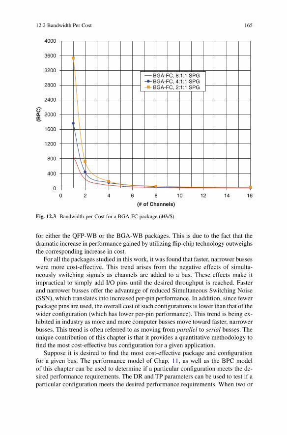
12.2 Bandwidth Per Cost 165
00 2 4 6 8 10 12 14 16
400
800
1200
1600
2000
2400
2800
3200
3600
4000
(# of Channels)
(BP
C)
BGA-FC, 8:1:1 SPGBGA-FC, 4:1:1 SPGBGA-FC, 2:1:1 SPG
Fig. 12.3 Bandwidth-per-Cost for a BGA-FC package (Mb/$)
for either the QFP-WB or the BGA-WB packages. This is due to the fact that thedramatic increase in performance gained by utilizing flip-chip technology outweighsthe corresponding increase in cost.
For all the packages studied in this work, it was found that faster, narrower busseswere more cost-effective. This trend arises from the negative effects of simulta-neously switching signals as channels are added to a bus. These effects make itimpractical to simply add I/O pins until the desired throughput is reached. Fasterand narrower busses offer the advantage of reduced Simultaneous Switching Noise(SSN), which translates into increased per-pin performance. In addition, since fewerpackage pins are used, the overall cost of such configurations is lower than that of thewider configuration (which has lower per-pin performance). This trend is being ex-hibited in industry as more and more computer busses move toward faster, narrowerbusses. This trend is often referred to as moving from parallel to serial busses. Theunique contribution of this chapter is that it provides a quantitative methodology tofind the most cost-effective bus configuration for a given application.
Suppose it is desired to find the most cost-effective package and configurationfor a given bus. The performance model of Chap. 11, as well as the BPC modelof this chapter can be used to determine if a particular configuration meets the de-sired performance requirements. The DR and TP parameters can be used to test if aparticular configuration meets the desired performance requirements. When two or

166 12 Optimal Bus Sizing
more configurations meet the performance requirements, their BPC values can nextbe used to select the most cost-effective configuration. Since these models avoid theuse of SPICE, the determination of the most cost-effective bus configuration can bedone very quickly. In addition, the BPC metric can provide a quick comparison ofthe cost-effectiveness of the available packaging options. The analytical models andsizing techniques presented can aid VLSI designers to quickly select the optimaloff-chip bus configuration.
12.3 Bus Sizing Example
In order to illustrate the use of the bus sizing technique, consider the example below.
Example 12.1 Consider an on-chip circuit that needs to transmit 2000 Mbs through
the package. Table 12.4 lists the modeled throughput results for the three packagesstudied in this work. From this table, it is clear that multiple configurations canmeet the 2000 Mb
s throughput requirement. The bus configurations that meet thethroughput requirement are:
• QFP-WB package with Wbus = 16 and SPG = 2:1:1• BGA-WB package with Wbus = 1 and SPG = 2:1:1• BGA-WB package with Wbus = 16 and SPG = 2:1:1• BGA-FC package with Wbus = 16 and SPG = 8:1:1• BGA-FC package with Wbus = 1 through 16 and SPG = 4:1:1• BGA-FC package with Wbus = 1 through 16 and SPG = 2:1:1
Using Table 12.3, it is quickly found that the BGA-WB with Wbus = 1 and SPG =2:1:1 is the least expensive configuration that will meet the throughput requirement.This is also apparent in Figs. 12.1, 12.2, and 12.3 which shows that this configurationhas a higher BPC than the QFP-WB and BGA-WB configurations. The BGA-FCconfigurations have higher BPC than the lowest cost BGA-WB configuration. Usingthe BGA-FC solution has the added advantage that the resulting solution providesadditional throughput margin, which is useful in the event that the bus throughputrequirement would increase in future revisions of the design.
Table 12.4 Modeled throughput results for packages studied ( Mbs )
Number of channels
Bus configuration 1 2 4 8 16
QFP-WB 8:1:1 458 324 372 410 820QFP-WB 4:1:1 916 569 677 777 1554QFP-WB 2:1:1 1832 959 1182 1430 2860BGA-WB 8:1:1 553 420 460 498 996BGA-WB 4:1:1 1106 750 835 935 1871BGA-WB 2:1:1 2213 1281 1437 1689 3378BGA-FC 8:1:1 1675 1303 1386 1513 3025BGA-FC 4:1:1 3349 2272 2446 2814 5628BGA-FC 2:1:1 6699 3696 4011 4976 9952

Chapter 13Bus Expansion Encoder
When determining the performance of an off-chip bus, the worst-case noise mag-nitude must be considered in order to ensure a robust digital system. Chapter 11presented an analytical model to predict the performance of an off-chip bus using theassumption that each of the noise sources within the package contributes its worst-case noise. Each source of noise within the package (Sect. 8.2) had a particular setof data sequences that resulted in the worst-case noise. This set of sequences dictatesthe highest performance that the package can achieve. The sequences that result innoise (from any noise source) above a certain magnitude can be avoided by designingan encoder which eliminates such sequences. This increases the performance of thepackage. By inserting this encoder in the signal path on the IC, it ensures that theoff-chip data is encoded before traversing the package interconnect. In this way, datasequences which result in noise above a specified limit can be avoided and the busperformance can be increased.
The encoder is constructed to remove any bus sequence which results in a noiseevent (regardless of the noise source) above a user-specified value. Experimentalresults demonstrate that this methodology improves the overall performance of thebus even after considering the overhead of the encoder circuit.
The technique maps each element in the original set of on-chip data sequencesto an element in an alternate set of sequences (whose noise is bounded by the user-specified limit). Since the alternate set of sequences has a width greater than the widthof the original bus, we refer to the resulting circuit as a bus expansion encoder. Theconstruction of the encoder/decoder utilizes an implicit, Reduced Ordered BinaryDecision Diagram (ROBDD). If it is desired that the noise due to one or more noisesources (described in Sect. 8.2) should be reduced, the method can by employed.
13.1 Constraint Equations
The first step in creating the bus expansion encoder is to create a set of constraintequations. The constraint equations are written so that arbitrary transitions can beevaluated for noise limit violations. When a transition is evaluated using the constraintequations and violates one of the user-defined noise limits, the transition is flaggedas illegal and is removed from the set of data sequences that are allowed to be
C. Duan et al., On and Off-Chip Crosstalk Avoidance in VLSI Design, 167DOI 10.1007/978-1-4419-0947-3_13, © Springer Science+Business Media LLC 2010

168 13 Bus Expansion Encoder
driven through the package interconnect. Each of the possible off-chip transitionsare evaluated against each of the constraint equations. The enumeration of the off-chip transitions is done implicitly, so as to increase the applicability of the technique.After the evaluation is complete, a subset of legal transitions remain which are usedin the construction of the encoder.
13.1.1 Supply Bounce Constraints
When a pin i in segment j is a VDD pin, it is required that the bounce magnitude dueto the electrical parasitics in the package must not exceed the user-defined noise limitPsupply. When the pin under evaluation is a VDD pin, a constraint equation is writtento determine if any transitions that occur on the bus segment will result in a violationof Psupply. The constraint equation takes into account the voltage noise due to the self-inductance of the VDD pin in addition to any mutual inductive or capacitive couplingthat occurs due to switching signals in adjacent pins. By multiplying the couplingmagnitude by the transition value v j
i (which can be 0, 1, or −1), the magnitude andsign of the induced noise value is accounted for. This handles the situation for a staticpin a static signal pin (v j
i = 0) which has no effect on the noise on the supply pin.The following constraint equation is written for any pin i within a bus segment j thatis used as a VDD pin, and is being evaluated for a supply bounce violation:
• v ji = VDD ⇒ Psupply · VDD ≥ ( di
dt
) ·[(L11) · (N1) +∑k=pL
k=−pL
[(M1(|k|+1)
)
× (v j
i+k
)]+∑k=pCk=−pC
[(C1(|k|+1) · Z2
0(0.8)
)·(
v ji+k
)]]
When a pin i in segment j is a VSS pin it is required that the bounce magnitude due tothe electrical parasitics in the package must not exceed the user-defined noise limitPgnd . When the pin under evaluation is a VSS pin, a constraint equation is written todetermine if any transitions that occur on the bus segment will result in a violation ofPgnd . The following constraint equation is written for any pin within a bus segmentj that is used for VSS and is being evaluated for a ground bounce violation:
• v ji = VSS ⇒ Pgnd · VDD ≥ ( di
dt
) · [(L11) · (N−1) +∑k=pLk=−pL
[(M1(|k|+1))
× (v j
i+k
)]+∑k=pCk=−pC
[(C1(|k|+1) · Z2
0(0.8)
)·(
v ji+k
)]]
13.1.2 Signal Coupling Constraints
13.1.2.1 Glitch Magnitude Constraints
When a pin i in segment j is a signal pin, it is required that the coupled voltage ontothat pin does not exceed any of the user-defined noise limits for signal coupling. Ifthe signal pin is static (v j
i = 0), then the glitch magnitude onto the victim pin mustnot exceed P0. As in the constraint equations for supply bounce, the magnitude of thecoupling contribution of any neighboring pin is multiplied by the transition value v

13.1 Constraint Equations 169
(which can be 0, 1, or −1) of the neighboring pin. This account for the magnitude andsign of the coupling due to the neighboring pin. The following constraint equationis written for any signal pin within a bus segment j that is static (v j
i = 0) and beingevaluated for a glitch violation:
• v ji = 0 ⇒ −(P0 · VDD) ≤ ( di
dt
) ·[∑k=pL
k=−pL
[(M1(|k|+1)) · (v j
i+k
)]
+∑k=pCk=−pC
[(C1(|k|+1) · Z2
0(0.8)
)· (v j
i+k
)]] ≤ (P0 · VDD)
13.1.2.2 Risetime Degradation Constraints
When a signal pin i in segment j transitions from a logic 0 to a logic 1 (v ji = 1), it
is required that the coupled voltage onto that pin does not hinder its risetime. In thissituation the cumulative value of the mutual coupling can be exploited to actuallyaid the transition on the victim signal pin. By requiring that the cumulative coupledvoltage on the victim pin either equals or exceeds the user-defined noise limit P1,it is also possible to improve the risetime of the victim signal (i.e., it is possible tospeed up the victim signal). By setting P1 to zero, it is guaranteed that the risetimefor the victim signal is not hindered. The following constraint equation is written forany signal pin within a bus segment j that is undergoing a rising transition (v j
i = 1)and is being evaluated for a rising edge degradation violation:
• v ji = 1 ⇒ P1 · VDD ≤ ( di
dt
) ·[∑k=pL
k=−pL
[(M1(|k|+1)) · (v j
i+k
)]
+∑k=pCk=−pC
[(C1(|k|+1) · Z2
0(0.8)
)· (v j
i+k
)]]
13.1.2.3 Falltime Degradation Constraints
In a similar manner, when a signal pin i in segment j transitions from a logic 1 toa logic 0 (v j
i = −1), it is required that the coupled voltage onto that pin does nothinder its falltime. By requiring that the cumulative coupled voltage on the victimpin either equals or exceeds the user-defined noise limit P−1, it is also possible toimprove the falltime of the victim signal (i.e., it is possible to speed up the victimsignal). By setting P−1 to zero, it is guaranteed that the falltime for the victim signalis not hindered. The following constraint equation is written for any signal pin withina bus segment j that is undergoing a falling transition (v j
i = −1) and being evaluatedfor a falling edge degradation violation:
• v ji = −1 ⇒ P−1 · VDD ≥ ( di
dt
) ·[∑k=pL
k=−pL
[(M1(|k|+1)) · (v j
i+k
)]
+∑k=pCk=−pC
[(C1(|k|+1) · Z2
0(0.8)
)· (v j
i+k
)]]

170 13 Bus Expansion Encoder
13.1.3 Capacitive Bandwidth Limiting Constraints
When a pin i in segment j is a signal pin, it is required that the capacitive bandwidthlimitation due to adjacent switching signal pins does not degrade the original risetimeby more than PBW. As described in Sect. 8.2.3, the capacitance that a victim signal willexperience will depend on the self-capacitance (C0) in addition to mutual couplingcapacitance to neighboring signal pins (C1k). The original risetime is defined asthe risetime achieved when all aggressing signals within the segment are static. Inthis case, the mutual capacitance to all other signal pins will be 1 · C1k . Whenthe neighboring aggressor pins switch, the resulting risetime of the victim can beeither improved, degraded, or unhindered (depending on the switching pattern of theaggressor pins).
The worst-case transition on the bus (which causes the largest risetime degra-dation on the victim) will be when all aggressor signal pins switch in the oppositedirection as the victim signal. This results in a doubling of the mutual capacitanceto all neighboring pins due to the doubling of the voltage excursion between sig-nals. This makes the capacitance to aggressing signal pins 2 · C1k . The best-casetransition on the bus (which causes the largest risetime improvement on the victim)will be when all signal pins switch in the same direction. In this case the couplingcapacitance between pins will be zero (0 · C1k) because there is no net voltagedifference across the pins. Since PBW is described as a percentage of risetime degra-dation, the constraint equation must account for the original risetime in addition tothe risetime which results when neighboring signals switch. The following constraintequation is written for any signal pin within a bus segment j that is undergoing apositive transition (v j
i = 1) and being evaluated for a capacitive bandwidth limitationviolation:
• v ji = 1 ⇒
PBW ≤[2.2 · (C0 +∑k=pC
k=−pCC1(|k|+1)
) · Z0
]−[2.2 · (C0 +∑k=pC
k=−pCC1(|k|+1) · (1 − v j
i+k
)) · Z0
]
[2.2 · (C0 +∑k=pC
k=−pCC1(|k|+1)
) · Z0
]
In the above constraint, multiplying the aggressor coupling capacitance by(1 − v j
i+k) handles the contribution of the mutual capacitance to the bandwidth lim-
itation. Since the aggressor signal pin can take on values of v ji+k ∈ {−1, 0, 1}, this
evaluates to (1 − v ji+k) ∈ {2, 1, 0}. This quantity is multiplied with C1k and then
added to C0 to give the total amount of capacitance that the victim pin charges.In a similar manner, the bandwidth limitation constraint can be written for a
victim signal that undergoes a falling transition (v ji = −1). In this case, the contri-
bution of the coupling capacitance is handled by multiplying the mutual capacitanceby (| −1 − v j
i+k |). Using this expression, the aggressor signal transition values
(v ji+k ∈ {−1, 0, 1}) evaluate to (| −1 − v j
i+k |) ∈ {0, 1, 2}. The following constraintequation is written for any signal pin i within a bus segment j that undergoes a falling

13.1 Constraint Equations 171
transition (v ji = −1) and is being evaluated for a capacitive bandwidth limitation
violation:
• v ji = −1 ⇒
PBW ≥[2.2 · (C0 +∑k=pC
k=−pCC1(|k|+1) · (| − 1 − v j
i+k |)) · Z0
]−[2.2 · (C0 +∑k=pC
k=−pCC1(|k|+1)
) · Z0
]
[2.2 · (C0 +∑k=pC
k=−pCC1(|k|+1)
) · Z0
]
13.1.4 Impedance Discontinuity Constraints
When a pin i in segment j is a signal pin it is required that the magnitude of the reflectedvoltage due to impedance discontinuities within the package must not exceed P� .As described in Sect. 8.2.5, the impedance of a given signal path will depend on itsself-inductance (L11) and self-capacitance (C0) in addition to any mutual inductance(M1k) and mutual capacitance (C1k). This means that the data sequences presenton neighboring signal pins will alter the effective inductance and capacitance ofthe victim signal. This directly effects the characteristic impedance of the victimpin, which is used in the evaluation of reflected noise. This must be accountedfor in the constraint equation. By multiplying this additional mutual inductanceand capacitance values by the transition values of the aggressor neighbors (v j
i+k),the polarity and cumulative effect of the coupling can be handled. The followingconstraint equation is written for any signal pin i within a bus segment j that undergoesa positive transition (v j
i = 1) and is being evaluated for an impedance discontinuityviolation:
• v ji = 1 ⇒ P� ≤
∣∣∣∣∣∣∣∣∣∣∣∣
√√√√L11 +∑k=pLk=−pL
(M1(|k|+1)) · (v ji+k
)
C0 +∑k=pCk=−pC
(C1(|k|+1)) · (v ji+k
) − Z0
√√√√L11 +∑k=pLk=−pL
(M1(|k|+1)) · (v ji+k
)
C0 +∑k=pCk=−pC
(C1(|k|+1)) · (v ji+k
) + Z0
∣∣∣∣∣∣∣∣∣∣∣∣
In a similar manner, when a pin i in segment j is a signal pin and undergoes a fallingtransition (v j
i = −1), it is required that the magnitude of the reflected voltage due toimpedance discontinuities within the package must not exceed P� . In this case thecontribution of the mutually coupled inductance and capacitance must be invertedto properly represent its cumulative nature. This is accomplished by multiplying themutual inductance and capacitance values by the negative of the transition value(−v j
i+k), thereby accounting for the polarity of the mutually coupled voltage. Notethat the polarity of � is reversed when the forcing function is a falling edge [97]. Thefollowing constraint equation is written for any signal pin i within a bus segment jthat undergoes a falling transition (v j
i = −1) and is being evaluated for an impedancediscontinuity violation:

172 13 Bus Expansion Encoder
• v ji = −1 ⇒ P� ≤
∣∣∣∣∣∣∣∣∣∣∣∣
√√√√L11 +∑k=pLk=−pL
(M1(|k|+1)) · (−v ji+k
)
C0 +∑k=pCk=−pC
(C1(|k|+1)) · (−v ji+k
) − Z0
√√√√L11 +∑k=pLk=−pL
(M1(|k|+1)) · (−v ji+k
)
C0 +∑k=pCk=−pC
(C1(|k|+1)) · (−v ji+k
) + Z0
∣∣∣∣∣∣∣∣∣∣∣∣
13.1.5 Number of Constraint Equations
For each VDD pin within a segment, one equation is written that represents thesupply bounce constraint (Psupply). For each VSS pin within a segment, one equationis written that represents the ground bounce constraint (Pgnd). For each signal pin,constraint equations are written for the three transition values that the pin can have(v j
i ∈ {−1, 0, 1}). When a signal pin is static (v ji = 0), one equation must be written
to constrain the glitching noise due to switching neighbor pins (P0). When a signalpin transitions high (v j
i = 1), three equations must be written that account forrising edge degradation (P1), capacitive bandwidth limitation (PBW), and impedancediscontinuities (P�). When a signal pin transitions low (v j
i = −1), three moreequations must be written that account for falling edge degradation (P−1), capacitivebandwidth limitation (PBW), and impedance discontinuities (P�). This gives the totalnumber of constraint equations that are written as:
Nconstraints = Np + Ng + (7 · Wbus) (13.1)
The number of constraints can be reduced for particular applications. For a particularpackage, some noise sources may be negligible and can be ignored in the constraintevaluation. For the three packages studied in this work, it was found that in all casesthe supply bounce and inductive signal coupling were the dominant noise sources.This is a consequence of noise being dominated by the inductance within the packageinterconnect. If only the inductive noise components are considered, then each signalpin needs only three constraint equations: P0, P1, and P−1. This reduces the numberof constraint equations to:
Nind–constraints = Np + Ng + (3 · Wbus) (13.2)
13.1.6 Number of Constraint Evaluations
Each of the constraint equations must be evaluated against each of the possibletransitions that are to be transmitted through the package. Since each signal pin cantake on three unique transition values (v j
i ∈ {−1, 0, 1}), then the total number ofpossible transitions for a given bus segment is bounded by:
Ntransitions = (Wbus + 2 · max(pL , pC))3 (13.3)

13.2 Encoder Construction 173
In practice, however, some of the signals in the neighborhood of the signal of interestmay be supply pins, resulting in fewer constraints. This gives the total number ofconstraint equation evaluations as:
Nevaluations = (Nconstraints) · (Ntransitions) (13.4)
Again, the number of evaluations can be reduced by limiting the noise sourcesthat are considered. It should be noted that due to the symmetry of the bus seg-ment representation (which mimics the regular manner in which the busses areimplemented in practice), the evaluations need only be performed on the signalswithin a single bus segment and not on the entire bus. This symmetry allows a dra-matic reduction in computation time compared to the case where the entire bus isanalyzed monolithically.
13.2 Encoder Construction
Once the transitions have been tested against all of the constraining equations, a subsetof legal transitions remain from the original set of possible transitions. Assume thatthe original set of constraints were written for a bus segment with n signals. Usingthe legal transitions remaining, we next find the maximum effective bus size m, suchthat the transitions on this bus can be encoded using the remaining legal transitionson the physical n-bit bus.
13.2.1 Encoder Algorithm
From the set of legal vector sequences, we next create a ROBDD [20, 22] G, toencode legal bus transitions. We then find the effective size m of the bus that canbe encoded using the transitions in G, using a ROBDD based algorithm. Note thatthe ROBDD G has 2n variables. The first n variables refer to the from vertices andthe next n variables refer to the to vertices of the vector transition. There is a legaledge between vertices v1 and v2 iff G(v1, v2) = 1.
Note that for a vector sequence v j, we can construct minterms in G to encodetransitions between vectors w j
from and w jto. The end-points of this edge (w j
from and
w jto) can be constructed given v j, as follows:
• w jfrom,i = 0 if v j
i = 1 (i.e. the signal is rising) or if v ji = 0 (i.e. the signal is static).
• w jfrom,i = 1 if v j
i = −1 (i.e. the signal is falling) or if v ji = 0 (i.e. the signal is
static).
Similarly, we can write
• w jto,i = 1 if v j
i = 1 or if v ji = 0.
• w jto,i = 0 if v j
i = −1 or if v ji = 0.
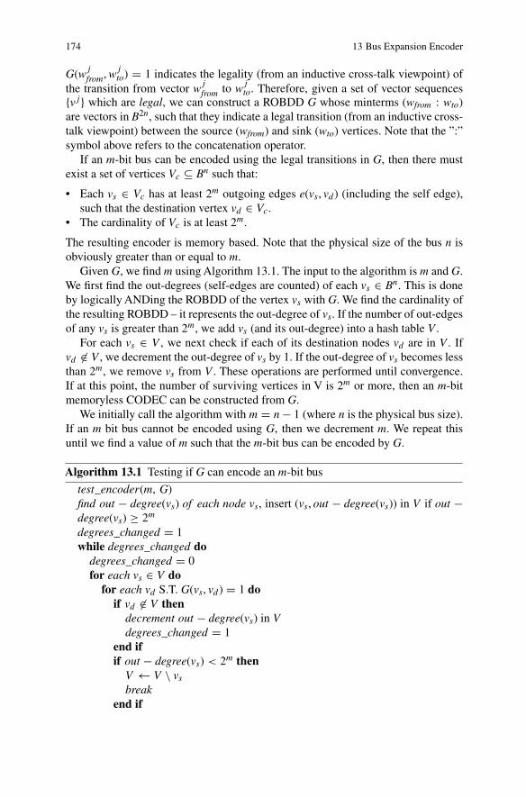
174 13 Bus Expansion Encoder
G(w jfrom, w j
to) = 1 indicates the legality (from an inductive cross-talk viewpoint) ofthe transition from vector w j
from to w jto. Therefore, given a set of vector sequences
{v j} which are legal, we can construct a ROBDD G whose minterms (wfrom : wto)are vectors in B2n, such that they indicate a legal transition (from an inductive cross-talk viewpoint) between the source (wfrom) and sink (wto) vertices. Note that the ”:”symbol above refers to the concatenation operator.
If an m-bit bus can be encoded using the legal transitions in G, then there mustexist a set of vertices Vc ⊆ Bn such that:
• Each vs ∈ Vc has at least 2m outgoing edges e(vs, vd) (including the self edge),such that the destination vertex vd ∈ Vc.
• The cardinality of Vc is at least 2m.
The resulting encoder is memory based. Note that the physical size of the bus n isobviously greater than or equal to m.
Given G, we find m using Algorithm 13.1. The input to the algorithm is m and G.We first find the out-degrees (self-edges are counted) of each vs ∈ Bn. This is doneby logically ANDing the ROBDD of the vertex vs with G. We find the cardinality ofthe resulting ROBDD – it represents the out-degree of vs. If the number of out-edgesof any vs is greater than 2m, we add vs (and its out-degree) into a hash table V .
For each vs ∈ V , we next check if each of its destination nodes vd are in V . Ifvd �∈ V , we decrement the out-degree of vs by 1. If the out-degree of vs becomes lessthan 2m, we remove vs from V . These operations are performed until convergence.If at this point, the number of surviving vertices in V is 2m or more, then an m-bitmemoryless CODEC can be constructed from G.
We initially call the algorithm with m = n − 1 (where n is the physical bus size).If an m bit bus cannot be encoded using G, then we decrement m. We repeat thisuntil we find a value of m such that the m-bit bus can be encoded by G.
Algorithm 13.1 Testing if G can encode an m-bit bus
test_encoder(m, G)find out − degree(vs) of each node vs, insert (vs, out − degree(vs)) in V if out −degree(vs) ≥ 2m
degrees_changed = 1while degrees_changed do
degrees_changed = 0for each vs ∈ V do
for each vd S.T. G(vs, vd) = 1 doif vd �∈ V then
decrement out − degree(vs) in Vdegrees_changed = 1
end ifif out − degree(vs) < 2m then
V ← V \ vs
breakend if

13.4 Experimental Results 175
end forend for
end whileif |V | ≥ 2m then
print(m-bit bus may be encoded using G)else
print(m-bit bus cannot be encoded using G)end if
For a memory-less encoder, the subgraph induced by the edges in Vc should be aclique. Memory-based encoders are explored in this work, due to the fact that theyallow effective widths which are higher than memory-less encoders.
Note that this entire analysis needs to be performed for a representative bus seg-ment. In other words, even if the bus is very wide, the analysis is performed for asingle segment, which is typically very small. This segment could be part of a muchlarger bus, and the analysis would be valid for all segments of the bus.
13.2.2 Encoder Overhead
The end result of the encoder construction is a mapping between transitions on anm-bit on-chip bus to transitions on an n-bit off-chip bus. The transitions on the n-bitoff-chip bus are selected so that the worst-case noise resulting from any of thesetransitions is less than or equal to the user-specified noise limit. Since the transitionson the n-bit bus avoid any noise greater than the user-specified limit, they can betransmitted at a higher datarate The net improvement must also account for theoverhead in the number of bits utilized for the bus (which is n−m). The computationof the overhead for the bus expansion encoding technique is shown in Eq. 13.5.
Overheadbus–expansion =(n − m
n
)· 100 (13.5)
13.3 Decoder Construction
The decoder construction is identical to the encoder construction however the processis performed in reverse. The combinational logic for the decoder is simply a reversepermutation of the logic for the encoder. In the case of the memory-less decoder, thelogic is induced by that of the encoder. This is also the case for the memory-baseddecoders.
13.4 Experimental Results
This section presents the experimental results that were performed to verify theeffectiveness of the bus expansion encoder.

176 13 Bus Expansion Encoder
13.4.1 3-Bit Fixed didt Example
The first example is a 3-bit bus that is evaluated for a fixed didt . This example illustrates
how the encoding technique directly reduces noise within the package. A didt of 33 MA
swas chosen that corresponds to a datarate of 550 Mb
s in a 50 � system using Eq. 11.6.The electrical parameters for the BGA-WB package are used from Table 9.1. Thebus configuration has three signal pins (Wbus = 3), one VDD pin (Np = 1), andone VSS pin (Ng = 1) for a total of 5 pins within the bus segment (Nsegment = 5).This configuration yields a Signal-to-Power-Ground metric of SPG = 3: 1: 1 and aSignal-to-Power-Ground Ratio of SPGR = 3. The mutual inductive and capacitivecoupling is considered to the 2 most adjacent pins (pL = pC = 2). This simplifiesthe analysis by ignoring inductive coupling less than 15% and capacitive couplingless than 50 fF. The bus configuration is shown in Fig. 13.1.
This bus was encoded using two sets of constraints: aggressive (Psupply, Pgnd , P0,P1, P−1, PBW, and P� set to 5%) and non-aggressive (Psupply, Pgnd , P0, P1, P−1,PBW, and P� set to 10%). The first step in the bus expansion technique is to writethe constraint equations. Equation 13.1 indicates that 24 constraint equations needto be written for this package; however, from the results in Chap. 11, it is known thatthe BGA-WB performance is dominated by the inductive nature of its interconnect.This allows the number of constraint equations to be reduced to 11 using Eq. 13.2.The following lists the 11 constraint equations for this example. These constraintshave been simplified by removing terms with v j
i = 0.
1) v j0 = VDD ⇒ Psupply · VDD ≤ di
dt · [(L11 · N1) + (M13 · v j−1
3
)+ (M12 · v j
1
)
+ (M13 · v j
2
)]
VDD VSSS S S
j-1 j j+1
VDD VSSS S S VDD VSSS S S
v 0j v 1
j v 2j v 3
j v 4j v 0
j+1 v 1j+1 v 2
j+1 v 3j+1 v 4
j+1v 0j-1 v 1
j-1 v 2j-1 v 3
j-1 v 4j-1
k12 k12
k13 k13
pL= 2 pL= 2
C12 C12
pC = 2 pC = 2
C13 C13
Fig. 13.1 3-Bit bus example

13.4 Experimental Results 177
2) v j1 = 1 ⇒ P1 · VDD ≤ di
dt · [(M12 · v j2
)+ (M13 · v j
3
)]
3) v j1 = −1 ⇒ P−1 · VDD ≥ di
dt · [(M12 · v j2
)+ (M13 · v j
3
)]
4) v j1 = 0 ⇒ −(P0 · VDD) ≤ di
dt · [(M12 · v j2
)+ (M13 · v j
3
)] ≤ (P0 · VDD)
5) v j2 = 1 ⇒ P1 · VDD ≤ di
dt · [(M12 · v j1
)+ (M12 · v j
3
)]
6) v j2 = −1 ⇒ P−1 · VDD ≥ di
dt · [(M12 · v j1
)+ (M12 · v j
3
)]
7) v j2 = 0 ⇒ −(P0 · VDD) ≤ di
dt · [(M12 · v j1
)+ (M12 · v j
3
)] ≤ (P0 · VDD)
8) v j3 = 1 ⇒ P1 · VDD ≤ di
dt · [(M13 · v j1
)+ (M12 · v j
2
)]
9) v j3 = −1 ⇒ P−1 · VDD ≥ di
dt · [(M13 · v j1
)+ (M12 · v j
2
)]
10) v j3 = 0 ⇒ −(P0 · VDD) ≤ di
dt · [(M13 · v j1
)+ (M12 · v j
2
)] ≤ (P0 · VDD)
11) v j4 = VSS ⇒ Pgnd · VDD ≤ di
dt · [(L11 · N−1) + (M13 · v j
2
)+ (M12 · v j
3
)
+ (M13 · vj+1
1
)]
All possible transitions on the bus are then evaluated using the 11 constraint equations.From this evaluation, transitions that violate any of the constraints are flagged asillegal and removed from subset of legal transitions used in the encoder construction.Table 13.1 shows the results of the constraint evaluations. In this table, if one of the
Table 13.1 Constraint evaluations for 3-Bit, fixed didt bus expansion example
Original transition Aggressive Non-aggressive
000 000 000001 001 00100-1 00-1 00-1010 010 010011 Violates 1,4 01101-1 01-1 01-10-10 0-10 0-100-11 0-11 0-110-1-1 Violates 4,11 0-1-1100 100 100101 Violates 1,7 10110-1 10-1 10-1110 Violates 1,10 110111 Violates 1,2,5,8 Violates 1111-1 Violates 1 11-11-10 1-10 1-101-11 Violates 1 1-111-1-1 Violates 11 1-1-1-100 -100 -100-101 -101 -101-10-1 Violates 7,11 -10-1-110 -110 -110-111 Violates 1 -111-11-1 Violates 11 -11-1-1-10 Violates 10,11 -1-10-1-11 Violates 11 -1-11-1-1-1 Violates 3,6,9,11 Violates 1

178 13 Bus Expansion Encoder
000
010
100
110
001
011101
111
{00-1, 001}
{010, 0-10}
{01-1, 0-11}
{10-1, -101}
{1-10, -110}
{100, -100}
{00-1, 001}
{00-1, 001}
{00-1, 001}
{01-1, 0-11}
{010, 0-10}
{010, 0-10}
{010, 0-10} {100, -100}
{100, -100}
{100, -100}
{10-1, -101}
{1-10, -110}
Fig. 13.2 Directed graph for the 3-Bit, fixed didt bus expansion example
original transitions violates a constraint equation, the number(s) of the constraintequation is listed.
After all transitions have been evaluated against the constraints, the remaininglegal transitions are used to create a directed graph. Figure 13.2 shows the directedgraph that was created from the non-aggressive constraint evaluation. This figuredoes not show the self-edges for simplicity.
From the directed graphs for both the non-aggressive and aggressive constraints,the largest effective bus width m was constructed, such that the noise for this busis within the user-defined limits. From the mapping between the transitions in them-bit bus to those in the legal transitions in the n-bit bus, the encoder state ma-chine is constructed. Figure 13.3 shows the overhead for the bus expansion encoder(Eq. 13.5) for both the aggressive and non-aggressive constraints. This figure sug-gests that the overhead of the encoder approaches an asymptotic limit as the numberof channels are added to the bus segment.
SPICE simulations were performed to quantify the noise reductions achievedby the encoder. Figure 13.4 shows the ground bounce reduction achieved by theencoder for both the aggressive and non-aggressive constraints. This figure shows
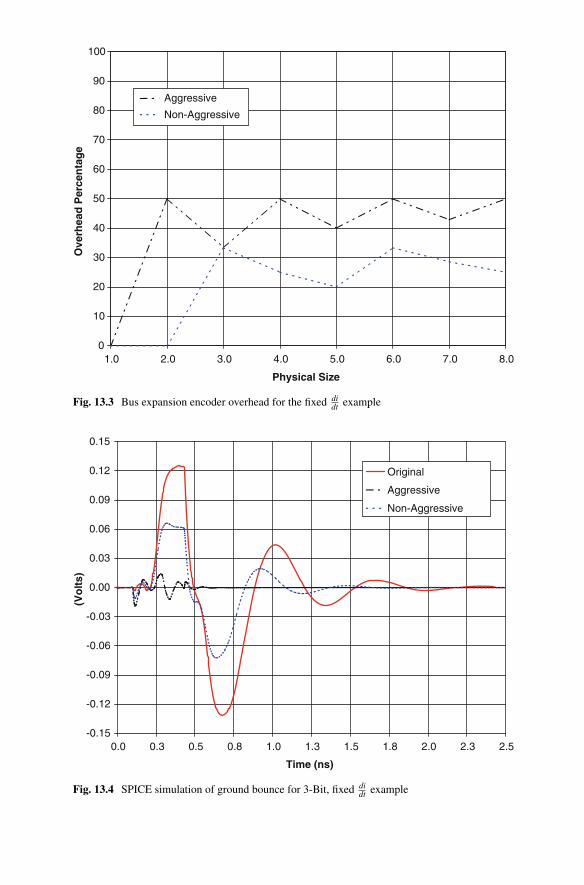
0
10
20
30
40
50
60
70
80
90
100
1.0 2.0 3.0 4.0 5.0 6.0 7.0 8.0
Physical Size
Ove
rhea
d P
erce
nta
ge
Aggressive
Non-Aggressive
Fig. 13.3 Bus expansion encoder overhead for the fixed didt example
-0.15
-0.12
-0.09
-0.06
-0.03
0.00
0.03
0.06
0.09
0.12
0.15
0.0 0.3 0.5 0.8 1.0 1.3 1.5 1.8 2.0 2.3 2.5
Time (ns)
(Vo
lts)
Original
Aggressive
Non-Aggressive
Fig. 13.4 SPICE simulation of ground bounce for 3-Bit, fixed didt example
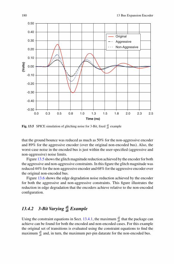
180 13 Bus Expansion Encoder
-0.50
-0.40
-0.30
-0.20
-0.10
0.00
0.10
0.20
0.30
0.40
0.50
0.0 0.3 0.5 0.8 1.0 1.3 1.5 1.8 2.0 2.3 2.5
Time (ns)
(Vo
lts)
Original
Aggressive
Non-Aggressive
Fig. 13.5 SPICE simulation of glitching noise for 3-Bit, fixed didt example
that the ground bounce was reduced as much as 50% for the non-aggressive encoderand 89% for the aggressive encoder (over the original non-encoded bus). Also, theworst-case noise in the encoded bus is just within the user-specified (aggressive andnon-aggressive) noise limits.
Figure 13.5 shows the glitch magnitude reduction achieved by the encoder for boththe aggressive and non-aggressive constraints. In this figure the glitch magnitude wasreduced 44% for the non-aggressive encoder and 68% for the aggressive encoder overthe original non-encoded bus.
Figure 13.6 shows the edge degradation noise reduction achieved by the encoderfor both the aggressive and non-aggressive constraints. This figure illustrates thereduction in edge degradation that the encoders achieve relative to the non-encodedconfiguration.
13.4.2 3-Bit Varying didt Example
Using the constraint equations in Sect. 13.4.1, the maximum didt that the package can
achieve can be found for both the encoded and non-encoded cases. For this examplethe original set of transitions is evaluated using the constraint equations to find themaximum di
dt and, in turn, the maximum per-pin datarate for the non-encoded bus.

13.4 Experimental Results 181
-0.50
-0.25
0.00
0.25
0.50
0.75
1.00
1.25
1.50
1.75
2.00
0.0 0.3 0.5 0.8 1.0 1.3 1.5 1.8 2.0 2.3 2.5
Time (ns)
(Vo
lts)
Original
Aggressive
Non-Aggressive
Fig. 13.6 SPICE simulation of edge coupling reduction for 3-Bit, fixed didt example
For the non-encoded evaluation, no vectors are removed from the original set;instead, di
dt is increased to its maximum value without violating any of the constraintequations. At that point, this di
dt indicates the fastest datarate that the non-encodedbus can achieve.
For the encoded evaluation, the reduced transition set from Sect. 13.4.1 is evalu-ated in the same manner. In the encoded case, the worst-case transitions have alreadybeen removed from the legal transition set and will result in a faster di
dt that can beachieved without violating any of the constraints. Table 13.2 shows the results for
Table 13.2 Experimental results for the 3-Bit, varying didt example
Original Encoded
Max di/dt 13.3 MA/s 37 MA/sMax Datarate 222 Mb/s 617 Mb/s# of Legal Transitions 27 13Physical Size of Bus 3 3Effective Size of Bus 3 2Encoder Overhead — 33%Bus Throughput 666 Mb/s 1234 Mb/sThroughput Improvement — 46%
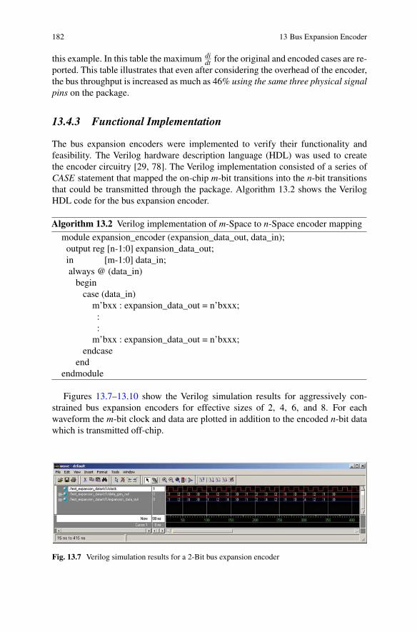
182 13 Bus Expansion Encoder
this example. In this table the maximum didt for the original and encoded cases are re-
ported. This table illustrates that even after considering the overhead of the encoder,the bus throughput is increased as much as 46% using the same three physical signalpins on the package.
13.4.3 Functional Implementation
The bus expansion encoders were implemented to verify their functionality andfeasibility. The Verilog hardware description language (HDL) was used to createthe encoder circuitry [29, 78]. The Verilog implementation consisted of a series ofCASE statement that mapped the on-chip m-bit transitions into the n-bit transitionsthat could be transmitted through the package. Algorithm 13.2 shows the VerilogHDL code for the bus expansion encoder.
Algorithm 13.2 Verilog implementation of m-Space to n-Space encoder mapping
module expansion_encoder (expansion_data_out, data_in);output reg [n-1:0] expansion_data_out;in [m-1:0] data_in;always @ (data_in)
begincase (data_in)
m’bxx : expansion_data_out = n’bxxx;::
m’bxx : expansion_data_out = n’bxxx;endcase
endendmodule
Figures 13.7–13.10 show the Verilog simulation results for aggressively con-strained bus expansion encoders for effective sizes of 2, 4, 6, and 8. For eachwaveform the m-bit clock and data are plotted in addition to the encoded n-bit datawhich is transmitted off-chip.
Fig. 13.7 Verilog simulation results for a 2-Bit bus expansion encoder

13.4 Experimental Results 183
Fig. 13.8 Verilog simulation results for a 4-Bit bus expansion encoder
Fig. 13.9 Verilog simulation results for a 6-Bit bus expansion encoder
Fig. 13.10 Verilog simulation results for a 8-Bit bus expansion encoder
13.4.4 Physical Implementation
In order to evaluate the feasibility of the expansion encoder/decoder, the physicaldesign of the circuitry was performed.
13.4.4.1 TSMC 0.13 μm ASIC Process
The encoders were synthesized using the TSMC 0.13 μm CMOS IC process to under-stand the impact on delay and area if the encoders were integrated on-chip. Encodersfor effective bus sizes of 2, 4, 6, and 8 were implemented. For each of these sizes,both the aggressive (5% of VDD) and the non-aggressive (10% of VDD) encoderswere synthesized. Table 13.3 lists the delay and area impact of the bus expansionencoders when implemented in a TSMC 0.13 μm process. This table illustrates that

184 13 Bus Expansion Encoder
Table 13.3 Bus expansion encoder synthesis results in a TSMC 0.13 μm process
Bus size (m) Noise limit
— 5% (aggressive) 10% (non-aggressive)
Delay (ns) 2 0.170 encoder not required4 0.670 0.5036 1.150 0.9558 1.310 0.983
Area (um2) 2 22 encoder not required4 152 1146 614 5098 1,181 886
incorporating the bus expansion encoder in a modern VLSI design results in a negli-gible area and delay penalty. The delay through the encoders is left unoptimized toillustrate the total combinational delay of the circuit; however, this delay can easilybe hidden by pipelining the encoder in order to partition the combinational delay.The decoder implementation results are identical to the encoder results.
13.4.4.2 Xilinx 0.35 μm FPGA Process
The encoders were also synthesized, mapped, and implemented for a Xilinx VirtexI-IPro, Field Programmable GateArray (FPGA) which used a 0.35 μm CMOS process.Figure 13.11 shows the Xilinx FPGA target that was used for implementation inaddition to the test setup for the encoders.
Encoders for effective bus sizes of 2, 4, 6, and 8 were implemented using boththe aggressive and non-aggressive constraints. Table 13.4 lists the delay and areaimpact of the bus expansion encoders when implemented in the FPGA process. In
Fig. 13.11 Xilinx FPGA target and test setup for encoder implementation

13.4 Experimental Results 185
Table 13.4 Bus expansion encoder synthesis results in a 0.35 μm, FPGA process
Bus size (m) Noise limit
— 5% (aggressive) & 10% (non-aggressive)
Delay (ns) 2 0.3514 1.0206 1.4508 1.610
FPGA Usage 2 <1%4 <1%6 <1%8 <1%
FPGA Implementation 2 3×, 2-Input FG’s4 6×, 4-Input FG’s6 9×, 6-Input FG’s8 12×, 8-Input FG’s
all cases the bus expansion encoder designs took less than 1% of the FPGA re-sources. The encoders were implemented using standard combinational logic blocks(Function Generators = FG’s) within the FPGA, which resulted in minimal propa-gation delay through the circuit. Again, the unoptimized delay is presented in thistable.
13.4.5 Measurement Results
The outputs of the FPGA were monitored using the 16950A Logic Analyzer fromAgilent Technologies, Inc. The logic analysis measurements verified that the encoderscould be taken from the concept to final implementation using standard IC designpractices. Figures 13.12–13.15 show the logic analyzer measurement results for theaggressively constrained bus expansion encoders for effective sizes of 2, 4, 6, and 8.
Fig. 13.12 Logic analyzer measurements of a 2-Bit bus expansion encoder
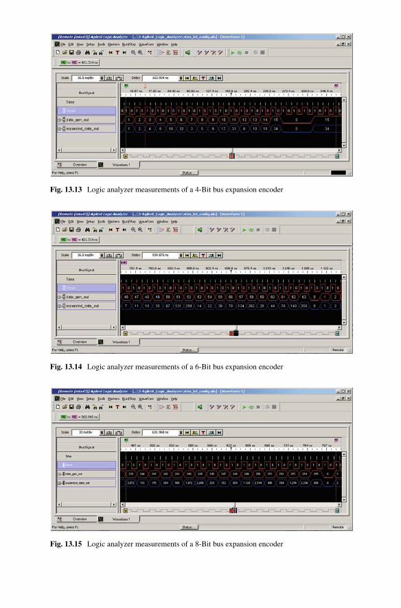
Fig. 13.13 Logic analyzer measurements of a 4-Bit bus expansion encoder
Fig. 13.14 Logic analyzer measurements of a 6-Bit bus expansion encoder
Fig. 13.15 Logic analyzer measurements of a 8-Bit bus expansion encoder

13.4 Experimental Results 187
For each waveform, the m-bit clock and data are plotted in addition to the encodedn-bit data which is transmitted off-chip. The m-bit vectors are monitored using adebug port that routes the internal nodes of the on-chip bus to the logic analyzer.In practice, this debug port would be removed so not to cause unintentional SSN.These figures show that the actual implementation results of the encoder match thefunctional simulations. For the bus configuration of this FPGA (SPG = 3 : 1 : 1), thenoise was reduced from 16% to 4% using the bus expansion encoding technique.
Chapter 14Bus Stuttering Encoder
It was shown in Chap. 13 that the performance of an off-chip bus could be increasedby avoiding a subset of patterns which resulted in noise greater than a specified limit.By eliminating the patterns that create the greatest amount of noise, the remain-ing patterns can be transmitted at a faster per-pin datarate without exceeding theuser-defined noise limits of the system. The bus expansion encoding technique wassuccessful in increasing the overall throughput of the bus even after considering theencoder overhead. The bus expansion encoder is ideal for applications where addi-tional signal pins on the package are available for use when encoding the on-chipvectors; however, in the case where the number of package signal pins equals theon-chip bus width, then a different approach can be used.
In this chapter a bus stuttering encoder is presented. In the stutter encoder, if back-to-back vectors (or states) that are being transmitted off-chip induce a transitionwhich results in a noise limit violation, an intermediate state is inserted betweenthem. This intermediate or stutter state offers a method to transition between thetwo original states (without directly switching between them) in such a manner thateach of the intermediate transitions do not result in a noise limit violation. It ispossible that more than one stutter state is required in some cases. In this fashion, thetransition between the original states is performed by inserting one or more stutterstates. During the time when the stutter states are being transmitted off-chip, theclock that is used to latch the data on the receiver is gated out. This assumes a sourcesynchronous data transmission scheme. This allows the receiver to be implementedusing standard circuitry. The receiver will only acquire valid data since it only latchesdata when a valid clock edge is present. The number of stutter states that are usedin the data transmission will depend on the aggressiveness of the user-defined noiselimits.
14.1 Encoder Construction
The steps in creating the stutter encoder are similar to those used in constructing thebus expansion encoder up to the point where the directed graph is processed. The userstill writes constraint equations which are evaluated for each possible transition on the
C. Duan et al., On and Off-Chip Crosstalk Avoidance in VLSI Design, 189DOI 10.1007/978-1-4419-0947-3_14, © Springer Science+Business Media LLC 2010

190 14 Bus Stuttering Encoder
bus. Transitions which result in a user-defined noise limit violation are removed fromthe subset of legal transitions. The remaining legal transitions are used to create thedirected graph G which represents all of the legal paths between any two vertices. Thegraph is represented implicitly and efficiently using ROBDDs [20, 22]. At this point,the user can run either the bus expansion algorithm or the bus stuttering algorithmon the directed graph G.
14.1.1 Encoder Algorithm
The encoder is constructed by evaluating each vertex vs of G(V , E) and finding theshortest path between vs and any destination vertex vd in G using only legal edgesof G (including self-edges). In order to be able to construct a stutter encoder, thefollowing conditions must hold:
• There must exist at least two outgoing edges (including the self-edge) for eachvs ∈ G.
• There must exist at least two incoming edges (including the self-edge) for eachvd ∈ G.
These requirements ensure that for the directed graph G, each vertex can reachat least one other vertex and can be reached by at least one other vertex. If theserequirements are not met, then the user must relax the user-defined noise limits untilboth conditions are met.
Given G, the algorithm first tests whether both of the above mentioned re-quirements are satisfied. The algorithm next attempts to determine the number ofintermediate steps required for a vertex vs ∈ G to reach another vertex vd ∈ G. Ifvd can be reached with just one edge, the algorithm records the transition as a directtransition (one that requires 0 stutter steps).
For the case where vs can not reach vd with only one edge, then at least onestutter state is needed to complete the transition. The algorithm then attempts to finda path between vs and vd using two edges. Since the set of vertices Vd that can bereached from vd by means of a direct path is known, the algorithm simply needs tofind an edge from vs to v ∈ Vd . Once such a path between vs and vd is found, thenthe algorithm records the intermediate vertex as a necessary stutter state which isrequired between vs and vd . This process is repeated for transitions which requiremore stutter states.
Algorithm 14.1 contains the pseudo-code for the stutter encoder algorithm.All transition_ path variables are initially initialized to be empty. The routinefind_ path(vs, vd , l) returns a shortest path from the source vs to destination vd , withpath_length l.
The maximum possible number of stutter states that may be used is (2Wbus − 1).This represents the worst-case where in order to transition from vs to vd , each andevery other vertex within G must be used as a stutter state. While this representsthe absolute theoretical worst case, experimental results have shown that the numberof stutter states is typically between 0 and 3 for bus segments up to 8-bits. In real

14.1 Encoder Construction 191
Algorithm 14.1 Constructing the stutter encoder
for (each vs ∈ V ) dofor (each vc ∈ V ) do
for (path_length = 1; path_length < 2Wbus−1; path_length + +) doif (transition_ path[vs, vd] == φ) then
transition_ path[vs, vd] = find_ path(vs, vd , path_length)end if
end forend for
end forfind_edge(vs, vd , l)if (∃v1, v2, · · · v(l−1)S.T .((vs, v1) ∈ E) ∧ ((v2, v2) ∈ E) ∧ · · · ∧ ((v(l−1), vd) ∈ E))then
return (vs, v1, v2, · · · , v(l−1), vd)else
return φ
end if
application of the stutter encoder, the actual number of stutter states that would everbe inserted within any data sequence is Wbus−1 since this represents the total numberof bits that could ever switch between two data vertices. It should be noted that thisanalysis is only performed on a representative bus segment (which is typically verysmall compared to the entire off-chip bus).
The construction of the encoder presented in this monograph is targeted at im-proving the performance of the off-chip data transmission. For this application, theshortest path between vertices is selected as the optimal choice for achieving maxi-mum throughput. This encoder can be modified for optimization of other constraintssuch as synthesis complexity, circuit area, or circuit delay by selecting other routesbetween vertices other than the shortest path.
14.1.2 Encoder Overhead
To calculate the overhead of the stutter encoder, it is assumed that each vector vs ⊆ Vhas an equal probability of occurring on the bus. Using this assumption, a sequenceof data patterns is constructed, in which each and every sequence occurs on the bus atleast once. When this sequence is transmitted, the minimum number of stutter statesare inserted in the transition between any pair of vectors. The maximum number ofstutter states that will be inserted in a sequence for any given encoder is 2Wbus−1.Equation 14.1 gives the overhead of the stutter encoder.
Overheadbus–stuttering =(∑2(Wbus−1)
k=1 (#Transitions Requiring k Stutters) · k
2(2·Wbus)
)· 100
(14.1)

192 14 Bus Stuttering Encoder
14.2 Decoder Construction
The stutter encoding technique assumes a source synchronous clocking architec-ture. In source synchronous clocking, the bus clock is generated at the transmitterand synchronized to the off-chip data being transmitted. The clock is then transmit-ted along with the data in the off-chip bus. By doing this, the timing correlationbetween the clock and data is extremely tight. This architecture has seen wide adop-tion in industry as a way to address channel-to-channel skew and common modenoise.
The stutter encoding technique is specifically designed for a source synchronousarchitecture. The encoding circuitry gates out the source synchronous clock whenstutter states are transmitted off-chip. Since the receiving circuitry only aquires dataon the rising edge of the source synchronous clock, the stutter states are ignored. Inthis manner, no special decoding circuitry is needed.
14.3 Experimental Results
To validate the feasibility of the stutter encoding technique, experimental resultswere performed on an example bus segment. For this example the off-chip bus wasimplemented using a BGA wire bonded package with parasitics given in Table 9.1.The off-chip bus uses a fixed di
dt of 8 MAs . Bus segments with between 2 to 8 signal
pins were encoded using the stuttering technique, assuming that each segment hadone VDD pin and one VSS pin. This bus was encoded using two sets of constraints –aggressive (Psupply, Pgnd , P0, P1, P−1, −PBW , and P� set to 5%.) and non-aggressive(Psupply, Pgnd , P0, P1, P−1, −PBW , and P� set to 10%). For these bus configura-tions and noise limits, all possible transitions were evaluated using the constraintequations described in Sect. 13.4. The remaining legal transitions were used in cre-ating the directed graph G which was used to construct the stuttering encoder. UsingAlgorithm 12, the shortest paths between all possible vertices were found. In addi-tion, the number of stutter states required to complete the intended transition werefound. Table 14.1 lists the percentage of transitions that require stutter states foreach of the bus sizes in this example. Using Eq. 14.1, the overhead of each of theencoders was calculated. Figure 14.1 shows the overhead of the stutter encoders asa function of bus segment size. Observe that for bus segment sizes less than 4-bits(aggressive constraints) and 6-bits (non-aggressive constraints), the overhead is lessthan 10%.
Figure 14.2 shows the bus throughput improvement when using the stutter en-coding technique. This figure shows the percentage of throughput improvement ofthe bus (including the overhead of the encoder). The improvement of the aggressiveencoder reaches 225% at a bus size of 6-bits. Beyond 6-bits, the overhead of the stut-ter encoder begins to outweigh the increased per-pin datarate (due to the increasingnumber of stutter states needed to avoid the noise limits).
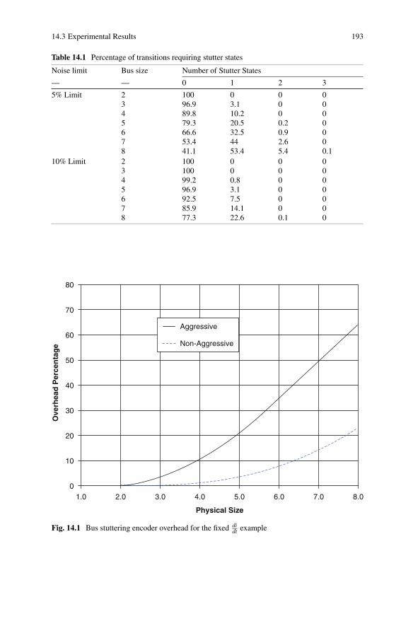
14.3 Experimental Results 193
Table 14.1 Percentage of transitions requiring stutter states
Noise limit Bus size Number of Stutter States
— — 0 1 2 3
5% Limit 2 100 0 0 03 96.9 3.1 0 04 89.8 10.2 0 05 79.3 20.5 0.2 06 66.6 32.5 0.9 07 53.4 44 2.6 08 41.1 53.4 5.4 0.1
10% Limit 2 100 0 0 03 100 0 0 04 99.2 0.8 0 05 96.9 3.1 0 06 92.5 7.5 0 07 85.9 14.1 0 08 77.3 22.6 0.1 0
01.0 2.0 3.0 4.0 5.0 6.0 7.0 8.0
10
20
30
40
50
60
70
80
Physical Size
Ove
rhea
d P
erce
nta
ge
Aggressive
Non-Aggressive
Fig. 14.1 Bus stuttering encoder overhead for the fixed didt example

194 14 Bus Stuttering Encoder
01.0 2.0 3.0 4.0 5.0 6.0 7.0 8.0
30
60
90
120
150
180
210
240
Physical Size
Th
rou
gh
pu
t Im
pro
vem
ent
(%)
Aggressive
Non-Aggressive
Fig. 14.2 Bus stuttering encoder throughput improvement
14.3.1 Functional Implementation
The bus stuttering encoders were implemented to verify their functionality and feasi-bility. Once again, the Verilog hardware description language was used to implementthe encoder circuitry [29, 78]. The implementation consists of a pipeline in whicheach stage of the pipe is routed to a multiplexer whose output drives the bus patternsoff-chip. A state machine monitors the incoming data from the core of the IC to checkwhether a stutter state is needed in the off-chip transmission. At the beginning ofcircuit operation, the output of the first pipeline stage is selected to be the output ofthe multiplexer. When a sequence of vectors occurs which require a stutter state, thenthe multiplexer is switched to the state machine input where the appropriate stutterstate is output. After the stutter state(s) is output, then the state machine switches themultiplexer back to the pipeline but now selects the next stage of the pipe. The statemachine continues to monitor the pipeline for illegal consecutive states and insertsthe appropriate number of stutter states in the off-chip data transmission. Duringthe time in which a stutter state is being selected as the output of the multiplexer,the control state machine gates out the source synchronous clock. By gating out theclock, it is ensured that the receiver will not latch any of the stutter states.
The pipeline in the stutter encoder is used to compare consecutive states withinthe data sequence. Each time that a stutter state is output on the bus, the encoded datasequence falls one clock period behind the original data. The depth of the pipelineis dependant on how many stutter states could potentially occur on the bus. The

14.3 Experimental Results 195
D Q D Q
n=1 n=2 n=3
D Q D Qdata_in[m:0]
clock_in
stutter_data_out[m:0]
stutter_stateControl StateMachine output_select
stutter_clock_outclock_qual
n
Fig. 14.3 Bus stuttering encoder schematic
bus protocol dictates the maximum length of consecutive data that could occur onthe bus. This, in turn, dictates the maximum depth of the pipeline that is needed toprevent overflow. In practice, bus protocols have scheduled idle periods when thepipeline can be reset [54, 77, 82]. For this work, 32 pipeline stages were used inthe implementation of the encoder. Figure 14.3 shows the schematic for the stutterencoder circuit.
Figures 14.4–14.6 show theVerilog simulation results for aggressively constrainedbus stuttering encoders for sizes of 4, 6, and 8 bits. For each waveform the originaldata and clock are plotted in addition to the encoded data and gated clock which aretransmitted off-chip.
Fig. 14.4 Verilog simulation results for a 4-Bit bus stuttering encoder
Fig. 14.5 Verilog simulation results for a 6-Bit bus stuttering encoder

196 14 Bus Stuttering Encoder
Fig. 14.6 Verilog simulation results for a 8-Bit bus stuttering encoder
14.3.2 Physical Implementation
In order to validate the feasibility of the stutter encoder, the physical design of theCODEC was performed.
14.3.2.1 TSMC 0.13 μm ASIC Process
The stutter encoders were synthesized using the TSMC 0.13 μm CMOS IC processto quantify their on-chip delay and area. Encoders for bus sizes of 4, 6, and 8 wereimplemented. For each of these sizes, both the aggressive (5% of VDD) and the non-aggressive (10% of VDD) stutter encoders were synthesized. Table 14.2 lists the delayand area impact of the bus stuttering encoders when implemented in a TSMC 0.13 μmprocess. This table shows that the stuttering encoder takes more area than the busexpansion encoder due to the state machines and pipeline stages associated with thedesign; however, when analyzing modern off-chip busses such as PCI Express, RapidI/O, and HyperTransport, it is found that all of these busses already contain pipelinestages and state machines to handle encoding/decoding required by the protocol. Thismeans that the stuttering encoder design could simply be included in the pre-existingstate machine and pipeline stages, thereby reducing the associated overhead.
In any case, the physical sizes are still negligible when considering reasonably-sized VLSI die sizes. For the largest stutter encoder listed in this table (8-bitaggressively encoded), the area consumed is still less than 1.5% of a 5 mm2 die.The un-optimized circuit delay is reported, which could be reduced using more
Table 14.2 Bus stuttering encoder synthesis results in a TSMC 0.13 μm process
Bus size Noise limit
— 5% (aggressive) 10% (non-aggressive)
Delay (ns) 4 2.02 1.996 2.42 2.388 2.85 2.79
Area (um2) 4 311k 310k6 362k 345k8 382k 368k

14.3 Experimental Results 197
Table 14.3 Bus stuttering encoder synthesis results for a Xilinx VirtexIIPro FPGA
Bus size Noise limit
— 5% (aggressive) & 10% (non-aggressive)
Delay (ns) 4 4.786 5.298 5.89
FPGA Usage 4 <1%6 <1%8 <1.5%
advanced circuit techniques. For the stutter encoder circuit, the combinational logicin the control state machine was the largest source of delay in the system.
14.3.2.2 Xilinx 0.35 μm FPGA Process
The encoders were also synthesized, mapped, and implemented for a Xilinx VirtexI-IPro, Field Programmable Gate Array (FPGA). Stutter encoders for bus sizes of 4,6, and 8-bits were implemented using both the aggressive and non-aggressive con-straints. Table 14.3 lists the delay and area impact of the bus stuttering encoders whenimplemented in the FPGA process. In all cases, the bus stuttering encoder designstook up less than 1.5% of the total FPGA resources.
14.3.3 Measurement Results
Once again, the test setup in Figure 13.11 was used to verify the actual performanceof the encoders. The outputs of the FPGA were again monitored using the 16950ALogic Analyzer from Agilent Technologies, Inc. Figures 14.7–14.9 show the logicanalyzer measurement results for aggressively constrained bus stuttering encoders
Fig. 14.7 Logic analyzer measurements of a 4-Bit bus stuttering encoder
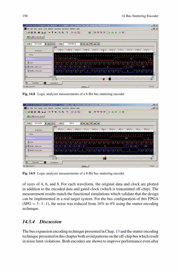
198 14 Bus Stuttering Encoder
Fig. 14.8 Logic analyzer measurements of a 6-Bit bus stuttering encoder
Fig. 14.9 Logic analyzer measurements of a 8-Bit bus stuttering encoder
of sizes of 4, 6, and 8. For each waveform, the original data and clock are plottedin addition to the encoded data and gated clock (which is transmitted off-chip). Themeasurement results match the functional simulations which validate that the designcan be implemented in a real target system. For the bus configuration of this FPGA(SPG = 3 : 1 : 1), the noise was reduced from 16% to 4% using the stutter encodingtechnique.
14.3.4 Discussion
The bus expansion encoding technique presented in Chap. 13 and the stutter encodingtechnique presented in this chapter both avoid patterns on the off-chip bus which resultin noise limit violations. Both encoders are shown to improve performance even after

14.3 Experimental Results 199
considering the overhead of the encoder. When to use one encoding scheme versusthe other depends on the application. The bus expansion encoder is aimed at genericoff-chip busses which do not contain any special data processing circuitry for theoff-chip transmission. In these cases, the encoder area impact is minimal since it isthe only circuitry placed in the path of the off-chip data.
The bus stuttering encoder is targeted at source synchronous, protocol basedbusses. In these cases, the pipeline and control state machines already exist to handlethe protocol of the bus. Adding stutter encoding capability to the preexisting circuitryis incremental and can potentially have less area impact than would the bus expansionencoder depending on how aggressively the noise is constrained.
To select the appropriate encoding technique, the designer must analyze the areaimpact on the design. For wider, parallel busses the bus expansion encoder is the betterchoice. For source synchronous, protocol based busses the bus stuttering encoder isthe better choice.

Chapter 15Impedance Compensation
Impedance mismatches between the IC package and the system PCB cause reflectionsthat lead to unwanted noise in the system. This noise limits the maximum dataratethat a package can achieve (Eq. 11.26). As described in Sect. 8.2, the impedance ofthe package interconnect is dictated by the self-inductance and self-capacitance of thephysical structure in addition to its mutual inductance and mutual capacitance withrespect to neighboring structures. Since the package interconnect was originallydeveloped for mechanical robustness, the electrical parasitics of the interconnectstructure can be considerable. In the majority of cases the resulting impedance of thepackage interconnect is not matched to that of the system. In addition, the mechanicalstructures are difficult to alter due to the complex manufacturing processes requiredto construct the interconnect. This makes it difficult and expensive to change thephysical structure of the package to match the characteristic impedance to that of thesystem PCB.
Chapters 13 and 14 presented bus encoding techniques that can reduce the effec-tive mutual inductive and mutual capacitive contributions to the impedance of a givensignal pin. This is accomplished by avoiding the switching patterns which inducenoise of a sufficiently high magnitude. This reduces the worst-case mutual inductiveand mutual capacitive coupling the bus. By reducing the coupling contribution for agiven signal pin, the variation in the impedance of the structure is reduced, therebyreducing the magnitude of the worst-case reflections from the package. While theseencoding techniques address the mutual coupling between signal pins in the package,they do not address the self-inductance and self-capacitance of the package struc-ture. As illustrated in Tables 9.1 and 9.2, the self-inductance and self-capacitanceof the interconnect structure contribute the majority of the electrical parasitics tothe characteristic impedance of the signal pin. Also illustrated in these tables is thatthe package interconnect is predominately inductive. The inductive nature of theinterconnect leads to a relatively high impedance when compared to the majority ofimpedances used in system PCBs, which typically range between 50 to 75 �. Thehigher impedance of the package pins cause positive reflections according to Eq. 8.13.
To reduce the impedance discontinuities introduced by the electrical parasiticsof the package interconnect, this chapter introduces an impedance compensationtechnique. In this technique, additional compensation capacitance is added near the
C. Duan et al., On and Off-Chip Crosstalk Avoidance in VLSI Design, 201DOI 10.1007/978-1-4419-0947-3_15, © Springer Science+Business Media LLC 2010
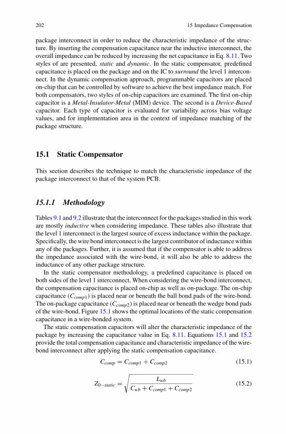
202 15 Impedance Compensation
package interconnect in order to reduce the characteristic impedance of the struc-ture. By inserting the compensation capacitance near the inductive interconnect, theoverall impedance can be reduced by increasing the net capacitance in Eq. 8.11. Twostyles of are presented, static and dynamic. In the static compensator, predefinedcapacitance is placed on the package and on the IC to surround the level 1 intercon-nect. In the dynamic compensation approach, programmable capacitors are placedon-chip that can be controlled by software to achieve the best impedance match. Forboth compensators, two styles of on-chip capacitors are examined. The first on-chipcapacitor is a Metal-Insulator-Metal (MIM) device. The second is a Device-Basedcapacitor. Each type of capacitor is evaluated for variability across bias voltagevalues, and for implementation area in the context of impedance matching of thepackage structure.
15.1 Static Compensator
This section describes the technique to match the characteristic impedance of thepackage interconnect to that of the system PCB.
15.1.1 Methodology
Tables 9.1 and 9.2 illustrate that the interconnect for the packages studied in this workare mostly inductive when considering impedance. These tables also illustrate thatthe level 1 interconnect is the largest source of excess inductance within the package.Specifically, the wire bond interconnect is the largest contributor of inductance withinany of the packages. Further, it is assumed that if the compensator is able to addressthe impedance associated with the wire-bond, it will also be able to address theinductance of any other package structure.
In the static compensator methodology, a predefined capacitance is placed onboth sides of the level 1 interconnect. When considering the wire-bond interconnect,the compensation capacitance is placed on-chip as well as on-package. The on-chipcapacitance (Ccomp1) is placed near or beneath the ball bond pads of the wire-bond.The on-package capacitance (Ccomp2) is placed near or beneath the wedge bond padsof the wire-bond. Figure 15.1 shows the optimal locations of the static compensationcapacitance in a wire-bonded system.
The static compensation capacitors will alter the characteristic impedance of thepackage by increasing the capacitance value in Eq. 8.11. Equations 15.1 and 15.2provide the total compensation capacitance and characteristic impedance of the wire-bond interconnect after applying the static compensation capacitance.
Ccomp = Ccomp1 + Ccomp2 (15.1)
Z0−static =√
Lwb
Cwb + Ccomp1 + Ccomp2(15.2)

15.1 Static Compensator 203
IC Substrate
On-Chip Capacitance (Ccomp1)
On-Package Capacitance (Ccomp2)
Wire Bond Parasitics (Lwb, Cwb)
Fig. 15.1 Cross-section of wire-bonded system with compensation locations
15.1.2 Compensator Proximity
In order to model the level 1 inductance and compensation capacitance as a singlelumped element, the compensation capacitance must reside within a certain distanceof the inductance. The maximum distance of the compensation capacitance from theinterconnect inductance depends on the frequency components present in the forc-ing function of the incident digital signal. If the compensation capacitance residesspatially close to the inductance, the resulting structure can be modeled as a lumpedelement, and the impedance of the structure is then deterministic. Typically, a struc-ture is considered a lumped element when its electrical length (i.e. its propagationdelay) is less than 20% of the highest risetime in the system [57]. Figure 15.2 showsthe physical length at which a structure can be treated as either a lumped or dis-tributed element as a function of risetime (for several common package materials).Given a particular risetime, physical lengths less than indicated in this plot are treatedas a lumped element. For physical lengths greater than this amount, the structure istreated as a distributed element. This plot considers the propagation delay of fourcommon dielectric materials that are used in VLSI packaging.
For VLSI risetimes less than 1ns, this plot shows that structures with electricallengths less than 200 ps can be treated as lumped elements. Since standard packagesubstrates utilize dielectric constants between Dk = 3 to Dk = 5, physical lengthsless than approximately 1 inch may be considered lumped elements. This means thatimplementing embedded capacitors within the package or IC substrate can directlyalter the characteristic impedance of the package interconnect (using a lumped modelto compute the altered characteristic impedance). Specifically, embedding capacitorson-chip or on-package will be utilized to alter the characteristic impedance of thepackage interconnect.
15.1.3 On-Chip Capacitors
Two styles of on-chip capacitors were evaluated for use to implement Ccomp1in the static compensator design. The first style of on-chip capacitor is called a

204 15 Impedance Compensation
0.00
0.15
0.30
0.45
0.60
0.75
0.90
1.05
1.20
1.35
1.50
0 0.1 0.2 0.3 0.4 0.5 0.6 0.7 0.8 0.9 1
Risetime (ns)
Ph
ysic
al L
eng
th (
inch
es)
FR4 (Dk=4)Nelco-13 (Dk=3.5)SPEEDBOARD (Dk=2.6)Rogers 4000 (Dk=3.4)
Fig. 15.2 Physical length at which structures become distributed elements
Device-based capacitor. This capacitor is created using the same process technologyutilized in creating an NMOS transistor. The lower conducting plate of the capacitoris the heavily doped, p-type channel of the silicon transistor. The insulating materialis the gate oxide of the NMOS transistor, which is a thin layer of silicon-oxide (SiO2)above the channel of the device. The upper plate of the capacitor is the PolySilicon(poly-Si) gate of the NMOS device. The drain and source terminals are connectedtogether and form one electrode of the capacitor, while the PolySilicon gate formsthe other electrode. This style of capacitor has a very high capacitance density due tothe thin plate separation which is identical to the gate thickness (tox) of the device. Inthis work, a 0.1 μm, BPTM process [1] is used to implement the on-chip capacitors.Using this technology, oxide layers as thin as 25 Å can be realized with a dielectricconstant of Dk = 3.9. This translates into a capacitance density of 13.7 fF/um2.
While the device-based capacitor achieves the highest density of any other style ofon-chip capacitor, it suffers from two major drawbacks. The first drawback is that thecapacitance value will change as a function of bias voltage. This nonlinearity is dueto the fact that as bias voltage changes, the device goes from cut-off to weak inversionand strong inversion. The nonlinearity of the capacitance as a function of bias voltageis a problem in digital applications, since the bias voltage typically varies from VSS toVDD. The second drawback of this style of capacitor is that it consumes valuable areawithin the IC that is normally reserved for the implementation of digital circuitry.

15.1 Static Compensator 205
The second type of on-chip capacitor studied in this work is called a Metal-Insulator-Metal (MIM) capacitor. In a MIM capacitor, an additional process step isused to form an extra metal layer in the upper layers of the IC (typically above metal3). This extra process step inserts an additional metal layer above the standard metal3 layer such that the insulator thickness between this new layer and metal 3 is muchlower than the inter-layer dielectric between metal 3 and 4. This extra step allowsthe creation of a parallel plate capacitor that uses a standard metal layer as the lowerplate (metal 3) and an additional MIM layer as the upper plate (metal 4’). Since theextra MIM layer is located spatially closer to the lower plate, a higher capacitancedensity is achieved compared to the capacitor with metal 3 and metal 4 plates. Inaddition, the extra MIM layer does not take up any routing area on metal 4. MIMtechnology is able to achieve plate-to-plate separations as thin as tox = 100 Å, whichtranslates into a capacitance density of 1.15 fF/um2. While MIM capacitors have alower capacitance density relative to device-based capacitors, their capacitance isconstant over the full range of bias voltages. This is because both plates within theMIM capacitor are formed with standard metal with passive materials between theplates.
For the static compensator, both styles of on-chip capacitors are investigated. Foreach capacitor, the nonlinearity with bias voltage and area utilization are quantified.Figure 15.3 shows the cross-section for both styles of on-chip capacitors.
15.1.4 On-Package Capacitors
Embedded PCB capacitors are evaluated to implement Ccomp2 in the static compen-sator design. An embedded PCB capacitor (EC) is simply a parallel plate capacitorthat is formed using standard metal layers within the PCB lamination. Embeddedcapacitors are preferred over surface mount (SMT) components due to the simplicityof their implementation. Since the capacitors are constructed using simple metal-to-metal area, no surface mount pads, loading process, or through-hole vias are needed.While ECs are easy to implement, they typically are only used for small values ofcapacitance (<10 pF). Standard PCB lamination processes are able to achieve plane-to-plane separation as low as 0.051 mm. Using a standard package dielectric such asFR4 (Dk = 4), this translates into a capacitance density of 420 fF/mm2. Table 15.1lists the capacitance densities and variation with bias voltages for all of the capacitorsused in the compensator design. For each capacitor, a reasonable size of capacitor isused for illistrative purposes.
15.1.5 Static Compensator Design
The static compensator is designed to alter the impedance of the largest inductivecomponent of the package interconnect (i.e., the wire-bond). It is assumed that if thisdesign methodology is successful in compensating for the wire-bond inductance, itwill also be successful in compensating for interconnect structures with less inductiveparasitics (i.e., flip-chip bumps).

206 15 Impedance Compensation
Substrate
p+ doped silicon
Device-BasedCapacitor
SiO2PolySilicon
v
NitrideAl (metal 4')
Al
Poly Layer
Metal 1 Layer
Metal 2 Layer
Metal 3 Layer
Metal 4 Layer
Al
Al
Al
Al
Metal 5 Layer
via
via
via
via
Al
via
Al
Al
via
via
Al
via
Al
MIM-BasedCapacitor
Fig. 15.3 On-chip capacitor cross-section

15.1 Static Compensator 207
Table 15.1 Density and linearity of capacitors used for compensation
Structure Cdensity Size Ctotal Notes
MIM-Based Capacitor 1.15 fF/um2 100 um2 11.5 pF tox = 600 Å(Si3N4), Dk = 7Device-Based Capacitor 2.7 fF/um2 100 um2 27 pF tox = 25 Å(SiO2), Dk = 3.9
(VGS = 0v)Device-Based Capacitor 13.8 fF/um2 100 um2 138 pF tox = 25 Å(SiO2), Dk = 3.9
(VGS = 1.5v)Embedded Capacitor 420 fF/mm2 0.5 mm2 0.105 pF tox = 0.051 mm(FR4), Dk = 4
Using the electrical parameters from Table 9.2 and solving Eqs. 15.1 and 15.2,the values of Ccomp1 and Ccomp2 for the static compensator can be found (assumingCcomp1 = Ccomp2). Table 15.2 lists the optimal capacitor values required to matchthe wire bond impedances (Table 9.2) to 50 �. Table 15.3 lists the correspondingsizes of the different types of capacitors required to realize Ccomp1 and Ccomp2. Thistable lists the sizes for both the MIM-based and Device-based on-chip capacitorimplementations of Ccomp1.
15.1.6 Experimental Results
In order to evaluate the performance of the static compensator, SPICE simula-tions were performed on all lengths of wire bonds listed in Table 15.2. Figure 15.4shows the simulated Time Domain Reflectrometry (TDR) of the static compensator(Eq. 8.14). A TDR simulation shows how much of a reflection (�) is caused by thewire bond. For each length of wire bond (1 to 5 mm), a 117 ps (3 GHz) input stepis used to stimulate the wire bond. In Fig. 15.4, the TDR waveforms are offset inthe voltage axis for view-ability with the 1 mm curve on the top and the 5 mm curve
Table 15.2 Static compensation capacitor values
Lengthwb(mm) Ccomp1(fF) Ccomp2(fF)
1 102 1022 208 2083 325 3254 450 4505 575 575
Table 15.3 Static compensation capacitor sizes
Lengthwb(mm) Ccomp1−MIM (μm) Ccomp1−Device(μm) Ccomp2−EC(μm)
1 10 × 10 2.7 × 2.7 388 × 3882 14 × 14 3.9 × 3.9 554 × 5543 18 × 18 4.9 × 4.9 692 × 6924 21 × 21 5.8 × 5.8 815 × 8155 24 × 24 6.5 × 6.5 921 × 921

208 15 Impedance Compensation
0.0
0.5
1.0
1.5
2.0
2.5
3.0
3.5
0.0 0.1 0.2 0.3 0.4 0.5 0.6 0.7 0.8 0.9 1.0
Time (ns)
Vo
ltag
e (V
)
No CompensationMIM-Based Static CompensationDevice-Based Static Compensation
Fig. 15.4 Static compensator TDR simulation results
on bottom. Reflections off of an inductive interconnect (i.e., ZL ≥ Z0) will result inthe waveform traveling above its steady state value. Reflections off of a capacitiveinterconnect (i.e., ZL ≤ Z0) will result in the waveform traveling below its steadystate value. For each length of wire bond the non-compensated, MIM-based, andDevice-based static compensation curves are shown. This figure shows the dramaticreduction in wire bond reflections when using a static compensator. Table 15.4 reportsthe reduction in reflections when using the static compensator(s).
Another way to observe the effect of the compensator is to observe the inputimpedance of the structure in the frequency domain. Figure 15.5 shows the inputimpedance of the wire bond structure versus frequency for the 3 mm wire bond. Inthis figure, the non-compensated, MIM-based, and Device-based static compensationcurves are again shown. To compare the performance we record the frequency atwhich the input impedance deviates by 10 � from the target impedance. In this case,
Table 15.4 Reflection reduction due to static compensator
Lengthwb(mm) �No−Comp(%) �MIM−Comp(%) �Device−Comp(%)
1 4.5 0.05 0.52 8.7 0.4 1.23 12.7 1.3 2.44 16.4 2.7 4.15 19.8 4.8 6.0

15.1 Static Compensator 209
30
40
50
60
70
80
90
100
110
120
130
101 100 1000 10000Frequency (MHz)
Zin
(O
hm
s)
No CompensationMIM-Based Static CompensationDevice-Based Static Compensation
Fig. 15.5 Static compensator input impedance simulation results
the compensators are designed to match the structure to 50 �. This figure illustratesthat adding a static compensator can keep the lumped impedance of the wire bondcloser to 50 � up to a much higher frequency. For this example, the 3 mm wirebond was kept to within 10 � of the target impedance (50 �) up to 4.8 GHz whenusing the MIM-based compensator (compared to only 3.1 GHz when considering theuncompensated wire bond).
Table 15.5 lists the frequencies at which the input impedance strays to +/−10 �
from the target for all of the lengths of wire bonds evaluated.These results show the dramatic reduction in impedance discontinuities when
using a static compensator. In all cases, the MIM-based compensator outperformedthe Device-based compensator.
Table 15.5 Frequency at which static compensator is +/−10 � from design
Lengthwb(mm) fNo−Comp(GHz) fMIM−Comp(GHz) fDevice−Comp(GHz)
1 9.3 14 122 4.7 7.1 5.73 3.1 4.8 3.84 2.4 3.7 2.95 1.9 3.0 2.5

210 15 Impedance Compensation
15.2 Dynamic Compensator
This section describes the technique used to match the impedance of the packageinterconnect to the characteristic impedance of the system.
15.2.1 Methodology
In the dynamic compensator methodology, capacitance is placed only on-chip(Ccomp1). The term dynamic means that the capacitance is programmable throughactive circuitry on the chip. The programmability of the compensation capacitanceallows the compensator to successfully match impedance across variations in thewire bond inductance. The programmability implies that the designer does not needto know the exact wire bond inductance prior to IC fabrication. This has the advan-tage that the dynamic compensator can accommodate process and design variation.In the dynamic compensator the net compensation capacitance is given by:
Ccomp = Ccomp1 (15.3)
Using Eq. 8.11 to describe the impedance of the dynamically compensated structure,the impedance of the wire bond becomes:
Z0−dynamic =√
Lwb
Cwb + Ccomp1(15.4)
15.2.2 Dynamic Compensator Design
The design of the dynamic compensator consists of CMOS pass gates that connectto integrated binary-weighted, on-chip capacitors. In this design there are three inte-grated capacitors (C1, C2 and C3) that can be switched in. The number of capacitorscan be increased, however experimental results indicate that sufficient resolution canbe achieved using just three capacitors. Each of these capacitors uses a pass gateto connect to the wire bond (Pass Gate #1, Pass Gate #2, Pass Gate #3). Each passgate has a control signal which either connects/isolates the capacitors to/from theon-chip I/O pad, which is connected to one end of the wire bond. Figure 15.6 showsthe schematic of the dynamic compensator design.
15.2.2.1 Capacitor Design
The diffusion regions associated with the pass gates contribute an additional capac-itance to Ccomp1, which must be considered in the design. For each of the threeprogrammable capacitor banks, the net capacitance will be the sum of the diffusion

15.2 Dynamic Compensator 211
Fig. 15.6 Dynamic compen-sator circuit
Pass Gate #1
C1
Pass Gate #2
C2
Pass Gate #3
C3
COff
CComp
Cntl(1)
Cntl(2)
Cntl(3)
capacitance of the pass gate and the integrated capacitor (Eqs. 15.5–15.7). If thepass gate of any bank i is turned off, then bank i simply contributes a capacitanceCpgi to Ccomp1.
CBank1 = Cpg1 + C1 (15.5)
CBank2 = Cpg2 + C2 (15.6)
CBank3 = Cpg3 + C3 (15.7)
To achieve a larger programming range, the integrated capacitors are binary-weightedsuch that:
CBank3 = 2 · CBank2 = 4 · CBank1 (15.8)
Using three control bits, 8 programmable values of capacitance can be connected tothe wire bond in increments of CBank1. COff is a constant, nonprogrammable capacitorwhich serves as an offset capacitance. It therefore sets the minimum capacitance

212 15 Impedance Compensation
value of the compensator. Using the conventions just described, the range of thecompensator can be described as:
Cmin = COff = Cpg1 + Cpg2 + Cpg3 (15.9)
Cmax = COff + CBank1 + CBank2 + CBank3 (15.10)
Cstep = CBank1 (15.11)
In this work the pass gates are implemented using a 0.1 μm CMOS process fromBPTM.As with the static compensator, the integrated capacitors (C1,C2, C3, COff ) areimplemented using the two different on-chip capacitance realization techniques thatare evaluated in this work (MIM-based and Device-Based). Both of these capacitortechniques are evaluated for range, area efficiency, and nonlinearity for applicationin the dynamic compensator design.
15.2.2.2 Pass Gate Design
As described in the previous section, the diffusion capacitance of the pass gates willcontribute to the total capacitance of each bank. The pass gate must be designedto have sufficient strength to drive the integrated capacitors (C1, C2, C3). TypicalCMOS design rules dictate that the pass gate sizing should be 1/3 of the size of anequivalent inverter that represents the integrated capacitor being driven [59]. Thisrule defines the amount of capacitance that will be present in each bank due to thepass gate and to the integrated capacitor.
Cpg = 1
3· CBank (15.12)
Cint = 2
3· CBank (15.13)
Using the Eqs. 15.5–15.13 and the values from Table 9.2, the sizing of the resultingcompensation circuitry can be determined. Table 15.6 lists the values of the capacitorsneeded in the dynamic compensator that will match the impedance of the wire bondto 50 � (Eq. 15.4).
Table 15.7 lists the device sizes of the dynamic compensator circuit. The capaci-tances C1, C2 and C3 are implemented as square devices for minimal area utilization.The total area of the compensator is computed as the size of the smallest enclosingsquare on the die. It is clear that the MIM-based dynamic compensator occupiesmore area than the Device-based compensator; however, the nonlinearity of both
Table 15.6 Dynamic compensation capacitor values
Lengthwb(mm) Ccomp1(fF)
1 2022 4033 6054 8065 1008

15.2 Dynamic Compensator 213
Table 15.7 Dynamic compensation capacitor sizes
MIM-Based Device-BasedComponent Area (W × L) Area (W × L)
Pass Gate #1 32.4 × 0.1 μm 32.4 × 0.1 μmPass Gate #2 62.5 × 0.1 μm 62.5 × 0.1 μmPass Gate #3 129.6 × 0.1 μm 129.6 × 0.1 μmCoff 8.5 × 8.5 μm 2.5 × 2.5 μmC1 11 × 11 μm 3.3 × 3.3 μmC2 15.5 × 15.5 μm 4.6 × 4.6 μmC3 22 × 22 μm 6.6 × 6.6 μm
Total 65 × 65 μm 25 × 25 μm
compensators must be analyzed to compare the applicability of the two circuits. Inthe next section, experimental results are presented that compare the two compensatordesigns.
15.2.3 Experimental Results
The same set of SPICE simulations as in the static compensator were performed onthe dynamic compensator to evaluate its performance.
Figure 15.7 shows the simulated TDR of the dynamic compensator (Eq. 8.14).Each length of wire bond (1 to 5 mm) is evaluated when stimulated with a 117 ps
0.0
0.5
1.0
1.5
2.0
2.5
3.0
3.5
0.0 0.1 0.2 0.3 0.4 0.5 0.6 0.7 0.8 0.9 1.0
Time (ns)
Vo
ltag
e (V
)
No CompensationMIM-Based Dynamic CompensationDevice-Based Dynamic Compensation
Fig. 15.7 Dynamic compensator TDR simulation results

214 15 Impedance Compensation
Table 15.8 Reflection reduction due to dynamic compensator
Lengthwb(mm) �No−Comp(%) �MIM−Comp(%) �Device−Comp(%) Setting
1 4.5 1.0 1.0 0012 8.7 1.8 1.3 0113 12.7 3.6 3.0 1004 16.4 4.3 3.3 1105 19.8 6.0 5.0 111
(3 GHz) input step. Again, the TDR waveforms are offset in the voltage axis forview-ability with the 1 mm curve on the top and the 5 mm curve on bottom. As in thecase of the static compensator, we can observe that the dynamic compensator resultsin a dramatic reduction in reflections from the wire bond.
Table 15.8 reports the reduction in reflections when using the dynamic compen-sator(s), along with the binary control setting used for the compensation.
Figure 15.8 shows the input impedance of the wire bond structure versus frequencyfor the 3 mm wire bond using the dynamic compensator. Once again, adding acompensator can keep the lumped impedance of the wire bond closer to 50 � upto a much higher frequency. In this case, the 3 mm wire bond was kept to within10 � of design up to 6.8 GHz when using the MIM-based compensator (compared to
30
40
50
60
70
80
90
100
110
120
130
100101 1000 10000Frequency (MHz)
Zin
(O
hm
s)
No CompensationMIM-Based Dynamic CompensationDevice-Based Dynamic Compensation
Fig. 15.8 Dynamic compensator input impedance simulation results

15.2 Dynamic Compensator 215
Table 15.9 Frequency at which dynamic compensator is +/−10 � from design
Lengthwb(mm) fNo−Comp(GHz) fMIM−Comp(GHz) fDevice−Comp(GHz) Setting
1 9.3 20 20 0012 4.7 10.1 10 0113 3.1 6.8 6.7 1004 2.4 5.2 5.1 1105 1.9 4.2 4.1 111
only 3.1 GHz when considering the uncompensated wire bond). The correspondingbandwidth of the Device-based compensator is 6.7 GHz.
Table 15.9 lists the frequencies at which the package impedance deviates +/−10 �
from its target impedance of 50 � for all wire bond lengths, using the dynamiccompensator.
Due to the nonlinearity of the Device-based capacitors and active pass gates,the variation of the dynamic compensator as a function of bias voltage was eval-uated. For each dynamic compensator setting, the bias voltage was changed forVG = 0v to VG = 1.5v, and the corresponding capacitance was recorded. Table 15.10lists the effect of bias voltage on both the MIM-based and Device-based compen-sator circuits. This clearly shows the nonlinearity of the Device-based compensatorwhich experiences as much as 33% capacitance variation when programmed toits maximum setting. This variation matches the expected variation of standardCMOS PolySilicon gate capacitors [59]. Note that the MIM capacitors also ex-hibit variability (3.8%), which occurs due to the bias dependence of the pass gatediffusion capacitances [2]. While both dynamic circuits exhibit a bias voltage depen-dence, both the compensators have sufficient range to cover wire bond lengths from1 to 5 mm.
These results illustrate that the Device-based compensator outperformed theMIM-based compensator when implemented in a dynamic architecture. Also, bothdynamic compensators outperformed their static counterpart. The dynamic compen-sator has the flexibility to be integrated in all future VLSI designs as part of thestandard process to reduce the growing impact of package reflections.
Table 15.10 Dynamic compensator range and linearity
MIM-Based Compensator Device-Based Compensator
Setting C(desired) C(Vbias=0v) C(Vbias=1.5v) Caverage C(Vbias=0v) C(Vbias=1.5v) Caverage(fF) (fF) (fF) (fF) (fF) (fF) (fF)
001 200 252 262 257 222 281 251010 325 373 382 378 318 414 366011 450 499 540 519 423 587 505100 575 588 596 592 485 651 568101 700 713 754 734 592 816 704110 825 828 895 862 688 968 828111 950 948 1041 994 788 1180 984
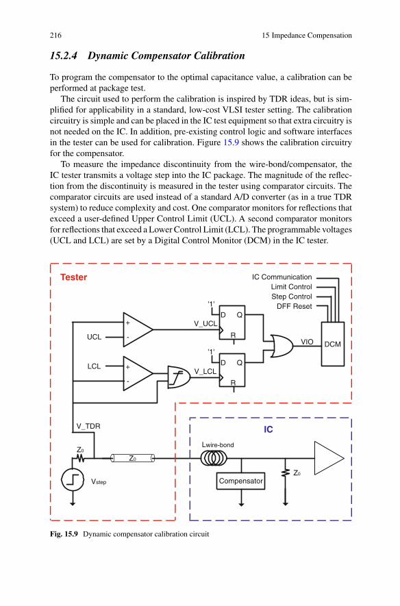
216 15 Impedance Compensation
15.2.4 Dynamic Compensator Calibration
To program the compensator to the optimal capacitance value, a calibration can beperformed at package test.
The circuit used to perform the calibration is inspired by TDR ideas, but is sim-plified for applicability in a standard, low-cost VLSI tester setting. The calibrationcircuitry is simple and can be placed in the IC test equipment so that extra circuitry isnot needed on the IC. In addition, pre-existing control logic and software interfacesin the tester can be used for calibration. Figure 15.9 shows the calibration circuitryfor the compensator.
To measure the impedance discontinuity from the wire-bond/compensator, theIC tester transmits a voltage step into the IC package. The magnitude of the reflec-tion from the discontinuity is measured in the tester using comparator circuits. Thecomparator circuits are used instead of a standard A/D converter (as in a true TDRsystem) to reduce complexity and cost. One comparator monitors for reflections thatexceed a user-defined Upper Control Limit (UCL). A second comparator monitorsfor reflections that exceed a Lower Control Limit (LCL). The programmable voltages(UCL and LCL) are set by a Digital Control Monitor (DCM) in the IC tester.
Compensator
Z0
Vstep
Z0
Lwire-bond
Z0
IC
+
-UCL
+
-
LCL D Q
R
'1'
D Q
R
'1'
DCMVIO
Tester IC CommunicationLimit ControlStep Control
DFF Reset
V_UCL
V_LCL
V_TDR
Fig. 15.9 Dynamic compensator calibration circuit

15.2 Dynamic Compensator 217
When a reflection from the wire-bond/compensator element is above/below theviolation limits, the comparator(s) will output a glitch signal that indicates a limitviolation (V_UCL / V_LCL). The limit violation glitch is fed into the clock input ofa D-flip-flop whose data input is tied to a logic 1. The D-flip-flop therefore serves asa trigger element that will switch and remain high when it detects any glitch fromthe comparators. The D-flip-flop output will remain high until reset by the DCM.The output of the two D-flip-flops are fed into an OR-gate to combine the upper andlower violation signals into one input (VIO) that is monitored by the DCM.
When the DCM detects a violation, it will communicate with the IC under test tochange the compensator settings. Once the compensator is adjusted, the D-flip-flopsare reset, and another voltage step is launched into the IC package. This process isrepeated until the magnitude of the reflections are within the LCL and UCL limits.
The lower control limit violation signal (V_LCL) is qualified using an AND-gate. The purpose of the AND-gate is to prevent glitches on V_LCL when the stepvoltage is below the LCL due to normal operating conditions such as the beginningof the rising edge of the step. The AND-gate is designed to have a high switch-pointsuch that Vswitchpoint−AND > LCL. Once the step voltage exceeds the switch-point ofthe AND-gate, the glitches from the comparator are allowed to pass through to theD-flip-flop. Spurious glitches which may be observed when the step voltage is belowthe AND gate switch-point are thus filtered out, and the glitches at the output of the
0.0
0.2
0.4
0.6
0.8
1.0
1.2
1.4
0.0 0.1 0.2 0.3 0.4 0.5 0.6 0.7 0.8 0.9 1.0
Time (ns)
Vo
ltag
e (V
)
V_TDRUCLLCLV_UCLVIO
Fig. 15.10 Dynamic compensator calibration circuit operation

218 15 Impedance Compensation
AND gate will therefore be solely due to reflections from the package (which violatethe LCL).
In the case that the compensator cannot find a setting that meets the reflectioncontrol limits, it will relax the UCL and LCL voltages. Since this calibration is onlyperformed on the signal pins of the IC package, the overhead associated with theprocess is small. The calibration can be sped up further by setting the UCL and LCLto predefined values that are based on the design of the IC and package. If the testeruses reasonable limits to begin with, the convergence of the algorithm will be sped up.
Figure 15.10 shows the signals of the calibration circuit during operation. In thiscase, the limits are set to indicate violations when reflections exceed 5%. In thisfigure, a UCL violation is indicated by a glitch on V_UCL. The glitch then triggersthe D-flip-flop which in turn sends a static control signal (VIO) to the DCM.

Chapter 16Future Trends and Applications
The analytical models and noise reduction techniques presented in Chaps. 11–15were analyzed for use with past, present, and future IC packaging in order to predictand improve performance. The experimental results illustrated that the techniqueswere successful and made significant improvement in the performance of the pack-aging. While these techniques were demonstrated to have an immediate impact whenapplied to commonly used VLSI packages, the current trends in IC technology makethese techniques even more invaluable. In addition, since all of the modeling andperformance techniques were described using a common mathematical framework,the work in this monograph can be easily applied to a wide variety of electronic ap-plications. This chapter presents some of the industry trends and other applicationsthat may benefit from the modeling techniques described in this work.
16.1 The Move from ASICs to FPGAs
Application specific integrated circuits (ASICs) have enabled the dramatic increasein computational power that digital systems have enjoyed over the past 20 years;however, within the past 5 years, the cost associated with designing and fabricat-ing an ASIC has increased considerably [40]. This cost stems from the increasedcomplexity of the design process, along with the high cost of manufacturing that ac-companies modern fabrication processes. As a consequence, there has been a markedreduction in the number of ASIC design starts per year compared to design starts 10years ago. At the same time, Field Programmable Gate Arrays (FPGAs) have gaineda foothold as one of the most-used building blocks in digital systems. The flexibilityof an FPGA allows designers to reduce hardware design cycles times, while addinginherent feature upgradeability in the final product. Traditionally FPGAs have beenused solely as a prototyping vehicle due to their higher cost and slower performancecompared to ASICs; however, recently FPGAs have experienced a dramatic increasein performance due to the rapid improvement in IC processing technology. FPGAdevelopment has kept up with Moore’s law, while at the same time providing in-herent design flexibility. Figure 16.1 shows that the doubling of transistors in Intelmicroprocessors has followed the prediction of Moore’s Law over the past 25 years
C. Duan et al., On and Off-Chip Crosstalk Avoidance in VLSI Design, 219DOI 10.1007/978-1-4419-0947-3_16, © Springer Science+Business Media LLC 2010

220 16 Future Trends and Applications
Fig. 16.1 Moore’s law prediction chart
[55]. Figure 16.2 shows the recent increase in the amount of logic cells that can beimplemented using an FPGA [101]. The rapid growth in FPGA technology illustrateshow FPGAs are also tracking Moore’s Law prediction.
Combining the increased performance of FPGAs with the dramatic increase inthe price of ASICs, FPGAs are now the preferred implementation vehicle for digitalsystems not requiring extremely high performance. Within the past 5 years the num-ber of digital design starts that use at least one FPGA is four times greater than the
Fig. 16.2 Xilinx FPGA logic cell count evaluation

16.1 The Move from ASICs to FPGAs 221
number of design starts requiring an ASIC [40]. This trend is important to this workdue to the use model of FPGAs. An FPGA is designed for use in a wide variety ofapplications, which each present different electrical constraints. A single FPGA mustoperate over various supply voltages, system impedances, bus speeds, and I/O levels.In addition, a particular FPGA circuit design is typically implemented in many stylesof packaging to offer a range of performance and cost to the users. This fact meansthat any technique that can improve system performance yet operate across manystyles of packaging and bus configurations will be extremely valuable to the FPGAindustry.
All of the techniques presented in this work can be applied to an FPGA. In fact, twoof these techniques were prototyped using FPGAs as well. Since the analytical modeland bus selection techniques presented in Chaps. 11 and 12 were constructed in termsof generic LC models of the package interconnect, they can be directly applied toany style of FPGA as long as the package parasitics are known. This enables systemdesigners to quickly analyze and design off-chip busses as well as understand theimpact of moving toward advanced packaging within an FPGA family.
The encoding techniques presented in Chaps. 13 and 14 can also be directlyapplied to FPGAs. Once a given bus configuration is implemented, performance canbe further increased by implementing an encoding scheme to avoid the noise inducedby bus data traversing the package parasitics. FPGAs lend themselves very well tothe encoding methodology since logic can be added after design and fabrication. Thisallows encoders to be added during prototyping if simultaneous switching noise isfound to be a problem. In addition, since the encoders can be added at anytime, theypresent the flexibility to address different noise sources depending on the type ofpackaging utilized. One FPGA in a system may have an inductive cross-talk noiseproblem while another FPGA may have an impedance discontinuity issue.Any sourceof noise that is of concern can be addressed by altering the encoder construction.
Finally, the compensator can also be used to directly improve performance inFPGAs. As mentioned earlier, an FPGA family is usually produced using the samedesign core, with various packaging, cost, and performance variants. This can beextremely challenging to VLSI designers who are faced with having to deal withmultiple package parasitics for a single circuit. An FPGA circuit may exist in a wirebonded package which must be impedance matched to the system impedance. This isdifficult to do since the same die may also be placed in a flip-chip package and mustbe impedance matched to the same system impedance. The dynamic compensatoraddresses this problem by having a programmable compensation capacitance thatcan be designed to cover a wide range of package parasitics. The dynamic compen-sator has the ability to match a wire bond package as well as a flip-chip packageto a given system impedance by simply changing the control lines of the capacitivecompensation.
All the techniques in this work favorably complement the trend of moving fromASICs to FPGAs. Since the manufacturing cost of ASICs is not predicted to lower inthe foreseeable future, FPGAs will continue to dominate digital design starts. Thisindicates that the work in this monograph is applicable to a dominant industry trendthat may continue for many decades.
222 16 Future Trends and Applications
16.2 IP Cores
Another recent trend in the VLSI industry is the move toward system design throughuse of Intellectual Property (IP) cores. An IP core is a circuit block that is designedand verified such that it can be dropped into a larger design. An IP core differsfrom standard ASIC designs in that it typically contains large, complex, system levelcircuitry. Blocks such as DDR memory controllers, PCI interfaces, and PowerPCmicroprocessors are examples of complex system-level IP cores. IP cores are alsogaining acceptance as stand-alone products which are licensed to an end user who isdesigning an FPGA or ASIC. The move toward the IP core methodology comes fromthe ever-growing complexity of modern VLSI designs. It is becoming impracticalfor a single design team to design every block in an ASIC in a reasonable amount oftime. As a consequence of time-to-market demands, design teams are turning to IPcores for the more standard portions of the ASIC.
The noise reduction techniques presented in this work lend themselves very ele-gantly to the IP core design methodology. Since each technique can be implementedusing a general purpose block of circuitry (which is relatively independent of theIC design), noise reduction cores can easily be created and incorporated into largerVLSI designs. In fact, these cores can be parameterized, allowing them to be effec-tive for more than one bus or package configuration. Bus encoding/decoding corescan be inserted between the core signals of the IC and package I/O pins. This coreinsertion would not have any impact on the core circuitry and serves only to improvethe speed of the off-chip bus that traverses the package. Integrated circuits that arelimited by the package noise can be sped up, so that the core logic on the die maybe operated faster as a consequence.
Similarly, the compensator can also be implemented as an IP core. Since thecompensator addresses the level 1 interconnect problem, the core circuitry of thedie can be designed without the additional constraints that are driven by packagingspeed limitations. In addition, since the compensator is shown to have sufficientrange to cover a variety of package interconnects, it can be used for designs that gointo multiple package technologies.
Figure 16.3 shows a possible scenario in which the techniques presented in thiswork can be integrated into a larger VLSI design as IP cores. In this example, twostyles of off-chip busses are shown. The first is a PCI bus, which is implemented usinga traditional wider, slower configuration. This style of bus experiences a large amountof supply bounce due to the large number of simultaneously switching signals. Forthis bus, an encoder is utilized to avoid inductive noise due to data sequences thattraverse the package. The second off-chip bus uses a HyperTransport core. Thisbus is implemented using a faster, narrower configuration. In this configuration, thenumber of signals that simultaneously switch is considerably less than the PCI bus.For this example, the HyperTransport bus will not experience as much supply bouncebut will instead be limited by capacitive bandwidth and impedance discontinuityproblems. To address the bandwidth limitation, an encoder is utilized to avoid theworst-case bandwidth limiting sequences. To address the impedance discontinuities,a compensator circuit is used to impedance match the package interconnect with the

16.3 Power Minimization 223
DieDie Die
Wire Bond Flip-Chip
uP
PCI Interface
Inductive Encoder
HyperTransport Interface
BW Encoder
Compensator
SRAM
Fig. 16.3 IP core design methodology incorporating encoder and compensator
system PCB. Since the noise reduction cores can be implemented in a parameterizedmanner, variations in the code construction allow the core to be usable in a varietyof packaging and bus configurations.
16.3 Power Minimization
Another major challenge for VLSI designers in this and the next decade is how toreduce the extreme amount of power that is being consumed as more transistors areintegrated on-chip. Advances in IC processing technology enables more transistorsto be integrated on a die than can be cooled using modern packaging techniques. Ad-ditionally, the ever-diminishing transistor feature sizes enable faster switching timesfor the core logic. Equation 16.1 expresses the dependence of power consumption onthe capacitance (Cload) being switched, supply voltage (VDD), switching frequency( fswitch), and the activity factor (αswitch).
PVLSI = (Cload) · ( fswitch) · (VDD)2 · (αswitch) (16.1)
The switching activity factor, αswitch, represents the fraction of circuit nodes thatswitch during any clock cycle. This parameter is typically between 0.2 and 0.35 formodern VLSI designs [59].

224 16 Future Trends and Applications
The encoders presented in this work were constructed in a general manner so as toeliminate any arbitrary vector sequence from the transmitted data. This methodologycan be easily extended to reduce power within the IC. As mentioned earlier, as muchas 25–50% of the IC power can be consumed in the output drivers [11, 40]. Since theencoders described in this monograph are designed to eliminate vector transitionsthat result in noise of a magnitude greater than a specified value, these encoderscan also be used to avoid data sequences which result in large power consumption.This has the effect of reducing αswitch in Eq. 16.1, thereby directly reducing powerconsumption.
A further extension of the encoder can be used to avoid vector sequences in on-chip busses which results in a power consumption above a specified limit. Longon-chip busses suffer not only an increased power consumption due to their typicallyhigh switching activity, but also from the fact that the bus capacitance (Cload) is pro-portional to bus length. The problem of long on-chip busses consuming considerablepower has become more important as more system level blocks are integrated withinone die. To incorporate complex system blocks, the die size increases, creating a needfor long block-to-block busses. These busses are inherently long therefore consumeconsiderable power, according to Eq. 16.1. Implementing encoders that reduce theworst-case power consumption sequences in long on-chip busses will have a directimpact on total power consumption of the IC. In addition, the encoder construc-tion methodology needs minimal modification, with addition constraint equationsrequired to express the user-defined power limits.
Since power is a critical issue in current and future designs, it is often conjecturedthat power will eventually limit the continued success of Moore’s Law. In sucha scenario, power reduction techniques like the one described above may play animportant part in extending the success of Moore’s Law
16.4 Connectors and Backplanes
Nearly all digital systems contain connectors which transmit signals and power be-tween various printed circuit boards. Connectors provide both the mechanical andelectrical connection between PCBs. Connector construction is similar in nature tothat of IC packaging in that the mechanical robustness of the interconnect must be ad-dressed before considering the electrical behavior. Once a stable mechanical structureis designed that can be economically manufactured, then the electrical performancecan be evaluated. This results in backplane interconnect that is not optimized for elec-trical performance. This is the exact situation that exists in IC packaging. Connectorleads contain electrical parasitics which degrade the performance of digital signals.Excess inductance and capacitance in the connector leads to voltage drop, capacitivebandwidth limitation, signal-to-signal coupling, and impedance discontinuities.
Since all the techniques presented in this work are constructed to alleviate thedetrimental effects of the inductance and capacitance of the interconnect, this nat-urally makes them applicable to any noise-prone electrical interconnect in a digitalsystem. The analytical modeling, encoding scheme, and compensation methodology

16.5 Internet Fabric 225
presented in this monograph can be applied to any connector without modification.Instead of using the inductance and capacitance parasitics from the IC package, theinductance and capacitance of the connector would be used. From these values, thenoise associated with the electrical parasitics of the connector can be directly com-puted. In addition, the encoding and compensation techniques can be used to boundthe maximum amount of connector noise.
The application of the noise reduction techniques to connectors plays well intothe backplane architecture used throughout industry. The backplane architecture isused widely throughout the computer industry as a way to scale systems. Smallercircuit blocks are implemented which can be plugged into a main PCB to add com-putational power as needed. Examples of circuit blocks that utilize this architectureare microprocessors, memory, and non-volatile storage elements. The backplanemethodology allows the smaller circuit blocks (which are utilized in the larger sys-tem) to be designed and verified independent of the larger system. This results in apartitioning of the system functionality and complexity, resulting in reduced designcycle times and more robust system operation. In addition, the smaller circuit blockscan be produced by multiple vendors, which drives down the cost of the design. Theadvantages of the backplane architecture have resulted in a widespread adoption ofthis methodology. This architecture has in turn driven the performance of some ofthe most popular off-chip bus standards. Busses such as PCI Express, Infiniband, andGigabit Ethernet were designed specifically to improve throughput of backplanes.These busses are predicted to achieve per-pin datarates of 10Gb/s within the next fiveyears [11, 77]. Since the techniques presented in this work apply directly to the con-nectors used in the backplane methodology, their importance could potentially playa crucial part in the continued increase in performance of backplane-based system.
16.5 Internet Fabric
One of the most important developments in the past 30 years has been the internet.This technology has revolutionized communication and sparked one of the longestgrowth periods for the global economy in recent history. One of the underlyingtechnologies that has enabled the success of the internet is the internet protocol.The internet protocol allows communication data to be broken into smaller piecesand transmitted as a series of packets, each of which contains destination addressinformation. The protocol allows data to be sent through multiple infrastructurepaths and be reassembled by the receiving computer. Packets may arrive out of orderon account of varying delays along different electrical paths. Various alternativeinfrastructure paths are selected according to the usage on any given path.
Many encoding protocols have been developed over the past decade to addressthe problem of congestion within the internet infrastructure (or fabric) [12, 48, 92].These protocols attempt to avoid network congestion by monitoring the sequence ofdata packets that are being transmitted. In applications such as audio and video, en-coding algorithms monitor the data stream for adjacent packets that contain identicalinformation. In an A/V application, sequential data patterns that contain the same

226 16 Future Trends and Applications
information may be eliminated without noticeable distortion in the final reassembleddata. These encoding algorithms allow streaming audio and video to be transmittedreliably and efficiently despite congested network fabrics, to be eventually receivedas a reasonable representation of the original data.
The encoders presented in this work are constructed by creating a directed graphcontaining transitions that have been deemed legal by the constraint equation evalu-ations. In the package noise constraints within this work, transitions are eliminatedfrom the complete set of encoder transitions if they violate any of the user-definednoise limits for the system; however, the constraint equations can be easily modifiedto detect sequences of data patterns that can be eliminated in anA/V application whenfaced with network congestion. This modification would consist of a new series ofconstraint equations that are written specifically for the A/V application. With theincreasing use of streaming audio and video over the internet, the encoding tech-niques presented in this work could potentially provide significant improvement inthe throughput of A/V data over congested network paths.
This chapter presented potential applications of the techniques in this work tocurrent and future industry trends. In each case, the general manner in which the noisereduction techniques are formulated enables their use in a variety of applications.Any system which experiences unwanted noise due to the electrical parasitics of theinterconnect or simply desires the elimination of specific transitions can benefit fromthe techniques presented in this monograph.

Chapter 17Summary of Off-Chip Crosstalk Avoidance
This monograph has presented a comprehensive look at the noise problems withinIC packaging. Today’s integrated circuits are experiencing a dramatic increase inperformance due to significant advances in the IC design and fabrication processes.IC technology has followed Moore’s Laws for the past 30 years and is expected tocontinue at this rate sometime into the next decade. At the same time, IC packagingtechnology has evolved at a much slower pace. This mismatch in performance be-tween the IC and the package is now the leading limitation to system performance.Inter-chip busses that transfer data between ICs within the system need to be slowedso as to avoid unwanted noise from the package. Off-chip communication is now thelargest bottleneck in modern digital systems design.
Unwanted noise occurs in the package due to the parasitic inductance and capaci-tance within the package interconnect. The parasitics of the package can cause supplybounce, signal-to-signal coupling, capacitive bandwidth limiting, and impedance dis-continuities. Since the IC packaging was originally developed for robust mechanicalperformance and manufacturability, the interconnect was not optimized for electricalperformance. In addition, the complex manufacturing processes used to create thepackage make altering the interconnect to improve electrical performance very diffi-cult and expensive. The move toward advanced packaging can reduce the electricalparasitics in the package but is often too expensive for the majority of VLSI designs.As such, any technique that can aid VLSI designers in the prediction of performanceand reduction of noise within the package is of great value.
Chapter 11 presented an analytical model to predict the performance of an ICpackage. This was accomplished by finding the fastest rate of change in currentor voltage that could be tolerated without violating any of the user-defined noiselimits. The amount of noise in the package is dependant on how large the parasiticinductance and capacitance are within the package interconnect. The electrical rateof change of current/voltage was translated a risetime figure and, in turn, into per-pindatarate and bus throughput. For each of the sources of noise, equations were derivedthat considered the package parasitics and the user-defined noise limits. To verifythe accuracy of the models, SPICE simulations were performed on a test circuit.It was found that the analytical model matched simulated results within 10% forbus segments up to 16-bits. It was also found that for the three packages studied
C. Duan et al., On and Off-Chip Crosstalk Avoidance in VLSI Design, 227DOI 10.1007/978-1-4419-0947-3_17, © Springer Science+Business Media LLC 2010

228 17 Summary of Off-Chip Crosstalk Avoidance
in this work, the inductive supply bounce and inductive signal coupling were thedominant noise sources. The analytical models derived in this chapter provide amethod for VLSI designers to quickly analyze different packaging technologies andbus configurations in order to meet their throughput requirements.
Chapter 12 presented a technique to select the most cost-effective bus configu-ration. Using the analytical models from Chap. 11 and including the per-pin costof the bus configuration, an algorithm was developed that could easily determinethe most cost-effective package selection and configuration. In addition, the met-ric of Bandwidth-per-Cost was introduced, which quantified the cost-effectivenessof a given bus. Using this metric, the total cost of different bus and package con-figurations (all of which meet the desired throughput) can be compared efficiently.The algorithm gives VLSI designers a powerful deterministic tool to find the mostcost-effective off-chip bus design.
Chapter 13 presented a bus expansion encoding technique that was able to reducepackage noise by encoding the data prior to it traversing the package interconnect.The encoder algorithm consisted of a series of constraint equations which werewritten to model noise violations for arbitrary bus transitions. These equations wereevaluated to indicate if a given transition would result in a noise limit violation whentraversing the package interconnect. Using the remaining legal transitions, a directedgraph was created that was used to construct the encoder. Each vertex within the graphwas evaluated in turn to find if its remaining outgoing edges were able to encode thetransitions of an m-bit bus. The output of the encoder is a mapping of transitions inthe original m-bit bus to transitions in an expanded n-bit bus, such that the transitionsin the expanded bus enable data transmission without noise violations.
Since the encoded data introduces less package noise, it can be transmitted at ahigher per-pin datarate. This speed increase results in throughput improvement evenafter accounting for the encoder overhead. Experimental results performed on theencoder illustrated that for a fixed di
dt of 33 MAs , package noise was reduced as much
as 89% for an aggressively encoded bus. It was also shown that for a 3-bit bus whichwas encoded and evaluated using a varying di
dt , the bus throughput was increasedup to 46% compared to the original unencoded data. The bus expansion encodingtechnique presented in this work provides VLSI designers a complete methodologyto reduce the noise within the IC package and increase off-chip bus throughput.
Chapter 14 presented a bus stuttering encoder which was also successful in reduc-ing the amount of package noise. This technique was similar to the bus expansionencoder in terms of the creation and evaluation of the constraints and legal transi-tions of the bus; however, a stuttering algorithm was invoked on the directed graph oflegal transitions, which inserted intermediate states between pairs of vertices whichresulted in noise limit violations. The stutter states were inserted such that eachvertex of the directed graph could transition to any other vertex using only the re-maining legal vectors. This encoder technique had the advantage that no additionalpackage pins were needed to encode the m-bit bus. This technique did require morearea on the IC than the bus expansion encoder, but was deemed to be incrementalto existing protocol-based busses that already contain state machines in their outputcircuitry. Experimental results illustrated that throughput could be increased as much

17 Summary of Off-Chip Crosstalk Avoidance 229
as 225% for a 6-bit, aggressively encoded bus. The bus stuttering encoder presentedin this work provides VLSI designers with a technique to improve throughput in theiroff-chip busses without adding pins to the package.
Chapter 15 presented a compensation technique that was able to match theimpedance of the package interconnect to that of the system PCB. This was accom-plished by adding additional capacitance near the wire bonds or flip-chips within thepackage. This has the effect of lowering the typically high interconnect impedanceto a level that matches the system PCB impedance. By matching the impedance ofthe package to the system PCB, reflections are avoided and performance can be in-creased. Static and dynamic compensation techniques were presented. In the staticapproach, predefined capacitance was placed on-chip and on the package to surroundthe inductive level 1 interconnect. The static compensator was able to reduce reflec-tions in a 5 mm wire bond from 20% to 5% for a risetime of 117 ps. In the dynamicapproach, a programmable capacitance was placed on-chip that could be altered afterIC fabrication. The dynamic technique allowed the same circuit to compensate forvarious interconnect inductances which may result from design or process variationsin the interconnect. It was demonstrated that the dynamic technique was able toreduce reflections of a 5 mm wire bond from 20% to 6% for a risetime of 117 ps.The compensators presented in this work offer VLSI designers a simple techniqueto impedance match the package interconnect to the system PCB without noticeablearea utilization within the package or on the die.
Chapter 16 gave an overview of other applications to which the techniques pre-sented in this work are well suited. The move from ASICs to FPGAs was described,along with a discussion of how the noise reduction techniques reported in this workapply directly to the FPGA design methodology. In addition, the utility of imple-menting the techniques as IP cores was discussed. The application of the encodersto the problem of power reduction within the IC was also presented. Finally, thepossible use of these techniques to connectors, backplanes, and the internet fabricwas pointed out. While only a subset of applications were presented in Chap. 16, itis believed that the techniques in this monograph can be applied to a wide variety ofelectronic applications due to their flexible formulation.
With the continued advancement in IC technology, the performance limitation ofthe package will continue to dominate system performance. While advanced pack-aging can aid in reducing the noise associated with the parasitics in the package,it is often too expensive for deployment in the majority of VLSI designs. Part IIor this monograph presented noise analysis and noise reduction techniques that canbe directly applied to current and future packaging technologies. With the use ofthe techniques presented in this monograph, the VLSI community can continue toexperience the dramatic increases in the computational power of digital systems.
References
[1] Berkeley predictive technology modeling homepage. http://www-device.eecs.berkeley.edu/bptm/.
[2] BSIM4 offcial release site. http://www-device.eecs.berkeley.edu/bsim3/bsim4.html.
[3] Fibonacci number (FromWikipedia). http://en.wikipedia.org/wiki/Fibonacci_number.
[4] Moore’s law. http://en.wikipedia.org/wiki/Moores_law.[5] Numeral system. http://en.wikipedia.org/wiki/Numeral_system.[6] Physical Design Modelling and Verification Project (SPACE Project). http://
cas.et.tudelft.nl/research/space/html.[7] TSMC 65 nm process. http://www.tsmc.com/english/b_technology/b01_
platform/b010101_65nm.htm.[8] TSMC 90 nm process. http://www.tsmc.com/english/b_technology/b01_
platform/b010101_90nm.htm.[9] Xilinx VIRTEX4 family datasheet. http://www.xilinx.com/products/silicon_
solutions/fpgas/virtex/virtex4/index.htm”.[10] 1958: The invention of the integrated circuit. Technical report, www.pcb.org,
2002.[11] The international technology roadmap for semiconductors (itrs). Technical
report, public.itrs.net, 2003.[12] A.S. Abraham, J. Wang, and J.C.L. Liu. Bandwidth-aware video encoding
with adaptive image scaling. In IEEE International Conference on Multimediaand Expo (ICME), pages 157–160, June 2004.
[13] J.H. Ahm, K.T. Lee, M.K. Jung, Y.J. Lee, B.J. Oh, S.H. Liu, Y.H. Kim,Y.W. Kim, and K.P. Suh. Integration of MIM capacitors with low-k/Cu processfor 90 nm analog circuit applications. In Proceedings of the IEEE InternationalInterconnect Technology Conference, pages 183–185, June 2003.
[14] N. Arora, K. Raol, R. Shcumann, and L. Richardson. Modeling and extractionof interconnect capacitance for multilayerVLSI circuits. In IEEE Transactionson Computer-Aided Design of Integrated Circuits and Systems, 15(1):58–67,1996.
[15] Avant! Raphael: Interconnect Analysis Program User’s Guide. www.avant!.com/raphael, 2000.
231
232 References
[16] D. Balaraman, J. Choi, V. Patel, P.M. Raj, I.R. Abothu, S. Bhattacharya,L. Wan, M. Swaminathan, and R. Tunimala. Simultaneous switching noisesuppression using hydrothermal barium titanate thin film capacitors. In Pro-ceedings of Electronic Components and Technology (ECTC), pages 282–288,June 2004.
[17] A. Bastani and C.A. Zukowski. A low-leakage high-speed monotonic staticCMOS 64b adder in a dual gate oxide 65-nm CMOS technology. In Pro-ceedings of International Symposium on Quality Electronic Devices, pages312–317, 2006.
[18] G.E. Beers and L.K. John. A novel memory bus driver/receiver architecture forhigher throughput. In Proceedings of the Eleventh International Conferenceon VLSI Design: VLSI for Signal Processing, pages 259–264. IEEE, 1998.
[19] B. Bollobas. Graph Theory. Springer-Verlag, New York, 1979.[20] K.S. Brace, R.L. Rudell, and R.E. Bryant. Efficient implementation of a BDD
package. In Design Automation Conference (DAC), pages 40–45, June 1990.[21] R.N. Bracewell. The Fourier Transform and its Applications. McGraw-Hill,
2000.[22] R.E. Bryant. Graph based algorithms for Boolean function representation.
In IEEE Transactions on Computers, volume C-35, pages 677–690, August1990.
[23] B. Casper. An accurate and efficient analysis method for multi Gb/s chip-to-chip signaling schemes. In Symposium of VLSI Circuits Digest of TechnicalPapers, pages 54–57, June 2002.
[24] B. Casper, A. Martin, J.E. Jaussi, J. Kennedy, and R. Mooney. An 8-Gb/ssimultaneous bidirectional link with on-die waveform capture. In IEEEJournal of Solid-State Circuits, volume 38, pages 2111–2120, December2003.
[25] J. Chem, J. Huang, L. Aldredge, P. Li, and P. Huang. Multilevel metal capac-itance models for CAD symbol design synthesis systems. In IEEE ElectronDevice Letter, 13:32–34, 1992.
[26] C.L. Chen and B.W. Curran. Switching codes for delta-I noise reduction. InIEEE Transactions of the 43rd IEEE Midwest Symposium on Circuits andSystems, volume 45, pages 1017–1021, September 1996.
[27] K.Y. Chou and M.J. Chen. Active circuits under wire bonding I/O padsin 0.13 μm eight-level Cu metal, FSG low-k inter-metal dielectric CMOStechnology. In IEEE Electron Device Letters, pages 466–468, October 2001.
[28] U. Choudhury and A. Sangivanni-Vincetelli. Automatic generation of analyt-ical models for interconnect capacitance. In IEEE Transactions on Computer-Aided Design, 14:470–480, 1995.
[29] M.D. Ciletti. Modeling, Synthesis, and Rapid Prototyping with the VerilogHDL. Prentice Hall, 1999.
[30] HyperTransport Consortium. Technical report, www.hypertransport.org,2005.
[31] W.H. Dally and J. Poulton. Transmitter Equalization for 4-Gbps Signaling. InIEEE Micro, volume 17, pages 48–56, February 1997.

References 233
[32] W.H. Dally and J. Poulton. Digital Systems Engineering. Cambridge Univer-sity Press, Cambridge, U.K., 1998.
[33] S. Das. Design Automation Techniques for Datapath Circuit. PhD thesis,University of Colorado, Boulder, Colorado, 2007.
[34] C. Duan, K. Gulati, and S.P. Khatri. Memory-based cross-talk cancelingCODECs for on-chip buses. In Proceedings of International Symposium onCircuits and Systems, pages 1119–1122. IEEE, May 2006.
[35] C. Duan and S.P. Khatri. Exploiting crosstalk to speed up on-chip buses. InProceedings of Design Automation, and Test in Europe (DATE) Conference,2004.
[36] C. Duan, A. Tirumala, and S.P. Khatri. Analysis and avoidance of cross-talk inon-chip bus. In Proceedings of the The Ninth Symposium on High PerformanceInterconnects, pages 133–138, 2001.
[37] SEMICON Far East. Technical report, www.semiconfarest.com, 2005.[38] I.M. Elfadel. On-chip bus interleaving revisited. In Proceedings of IEEE 14th
meeting on electrical performance of electronic packaging, 2005.[39] M. Ghoneima and Y. Ismail. Optimum positioning of interleaved repeaters in
bidirectional buses. Transactions on Computer-Aided Design, 24(3):461–469,2005.
[40] Agilent Technologies, Inc. Packaging Group. Personal communication, 2004.Ft. Collins, CO.
[41] R. Gupta. Deep-submicron challenges. In IEEE Design and Test of Computers,2002.
[42] L. He and K.M. Lepak. Simultaneous shield insertion and net ordering for ca-pacitive and inductive coupling minimization. In Proceedings of InternationalSymposium on Physical Design, pages 55–60.
[43] L. He and M. Xu. Characteristics and modeling for onchip inductive coupling.Technical Report ECE-00-1, Univeristy of Wisconsin at Madison, Madison,WI, 2003.
[44] K. Hirose and H. Yasuura. A bus delay reduction technique consideringcrosstalk. In Proceedings of the conference on Design, automation and test inEurope, pages 441–445, Paris, France.
[45] R. Ho, K. Mai, and M. Horowitz. Efficient on-chip global interconnects. InProceedings of Symposium on VLSI Circuits, pages 271–274, 2003.
[46] J.M. Hobbs, H. Windlass, V. Sundaram, S. Chun, G.E. White, M. Swami-nathan, and R.R. Tummala. Simultaneous switching noise suppression forhigh speed systems using embedded decoupling. In Proceedings of the 51stElectronic Components and Technology Conference, pages 339–343, June2001.
[47] M. Horowitz, C. Yang, and S. Sidiropoulos. High-speed electrical signaling:Overview and limitations. In IEEE Micro., volume 18, pages 12–24, January1998.
[48] A.A.M. Ibrahim. Statistical rate control for efficient admission control ofMPEG-2 VBR video sources. In IEEE Proceedings of the ATM Workshop,pages 26–29, May 1998.
234 References
[49] Actel Inc. Simultaneous switching noise and signal integrity. Technical report,www.actel.com, 2004.
[50] Agilent Technologies Inc. Advanced design systems user’s manual. http://www.agilent.com/ads, 2000.
[51] ASAT Inc. Peak Performance Array Packages. Technical report,www.asat.com, 2004.
[52] ASAT Inc. Peak Performance Enhanced Lead Packages. Technical report,www.asat.com, 2004.
[53] ASAT Inc. Peak Performance Flip Chip Packages. Technical report,www.asat.com, 2004.
[54] Intel Inc. Intel itanium 2 processor. Technical report, www.intel.com, 2003.[55] Intel. Prediction to reality. Technical report, www.intel.com, 2005.[56] Y. Iraqi, R. Boutaba, and R. Dssouli. Statistical properties of MPEG video
traffic and their impact on bandwidth allocation in wireless ATM networks.IEEE Wireless Communications and Networking Conference (WCNC), pages998–1002, September 1999.
[57] H. Johnson and M. Graham. High-Speed Digital Design. Prentice Hall PTR,2003.
[58] H. Johnson and M. Graham. High-Speed Signal Propagation. Prentice HallPTR, 2003.
[59] S. Kang and Y. Lebledici. CMOS Digital Integrated Circuits, 2nd edition.McGraw-Hill Companies, 1999.
[60] H. Kaul, D. Sylvester, and D. Blauuw. Active shielding of RLC global inter-connects. In International workshop on Timing issues in the specification andsynthesis of digital systems.
[61] S.P. Khatri. Cross-talk Noise Immune VLSI Design using Regular Layout Fab-rics. PhD thesis, University of California at Berkeley, Berkeley, California,1999.
[62] S.P. Khatri, A. Mehrotra, R.K. Brayton, Ralf H.J.M. Otten, and A.L.Sangiovanni-Vincentelli. A novel vlsi layout fabric for deep sub-micron ap-plications. In Proceedings of Design Automation Conference, pages 491–496.IEEE, 1999.
[63] H. Kim, Y. Jeong, J. Park, S. Lee, and J. Hong. Significant reduction ofpower/ground inductive impedance and simultaneous switching noise byusing embedded film capacitor. Transactions on Electrical Performance ofElectronic Packaging, pages 129–132, October 2003.
[64] H. Kim, B.K. Sun, and J. Kim. Suppression of GHz range power/groundinductive impedance and simultaneous switching noise using embedded filmcapacitors in multilayer packages and PCBs. In IEEE Microwave and WirelessComponents Letters, volume 14, pages 71–73, February 2004.
[65] K. Kim, K. Baek, N. Shanbhag, C. Liu, and S. Kang. Coupling-driven signalencoding scheme for low-power interface design. In Proceedings of Interna-tional Conference on Computer Aided Design, pages 318–321. IEEE/ACM,2000.

References 235
[66] C. Kinnaird. Standards are key to optimizing high-speed data bus communi-cations. Planet Analog (planetanalog.com), October 2002.
[67] L. Li, N. Vijaykrishnan, M. Kandemir, and M.J. Irwin. A crosstalk awareinterconnect with variable cycle transmission. In Proceedings of Designautomation and test in Europe, pages 102–107, 2004.
[68] J. Lin. Challenges for socdesign in very deep submicron technologies. Inter-national Conference on Hardware/Software Codesign and System Synthesis,2003.
[69] M. Lopez, J.L. Prince, and A.C. Cangellaris. Influence of a floating planeon effective ground plane inductance in multilayer and coplanar packages. InIEEE Transactions on Advanced Packaging, volume 22, pages 182–188, May1999.
[70] A.C.W. Lu, W. Fan, L. Wai, C.K. Wang, and H.G. Low. Design optimizationof wire bonding for advanced packaging. In Proceedings of Electronic Com-ponents and Technology Conference, pages 1364–1372. ACM/IEEE, May2003.
[71] J. Madsen and S. Long. A high-speed interconnect network using ternarylogic. In Proceedings of 25th International Symposium on Multi-Value Logic.IEEE, January 1995.
[72] C. Mattei and A.P. Agrawal. Electrical characterization of BGA packages. InProceedings of the 47th Electronic Components and Technology Conference,pages 1087–1093, May 1997.
[73] E. Mejia-Motta, F. Sandoval-Ibarra, and J. Santana. Design of CMOS buffersusing the settling time of the ground bounce voltage as a key parameter. InProceedings of the 43rd IEEE Midwest Symposium on Circuits and Systems,volume 2, pages 718–721, August 2000.
[74] M. Miura, N. Hirano, Y. Hiruta, and T. Sudo. Electrical characterization andmodeling of simultaneous switching noise for leadframe packages. In Pro-ceedings of the 45th Conference on Electronic Components and Technology,pages 857–864, May 1995.
[75] M. Mutyam. Preventing crosstalk delay using Fibonacci representation. InInternational Conference on VLSI Design, pages 685–688, January 2004.
[76] L. Nagel. Spice: A computer program to simulate computer circuits. InUniversity of California, Berkeley UCB/ERL Memo M520, May 1995.
[77] PCI-SIG Trade Organization. Technical report, www.pcisig.com/, 2004.[78] S. Palnitkar. Verilog HDL - A Guide to Digital Design and Synthesis. SunSoft
Press, 1996.[79] M.D. Powell and T.N. Vijaykumar. Pipeline damping: a microarchitectural
technique to reduce inductive noise in supply voltage. In Proceedings of the30th International Symposium on Computer Architecture, pages 72–83, June2003.
[80] J. Prasad, M. Anser, and M. Thomason. Electrical characterization of di-electrics (oxide, nitride, oxy-nitride) for use in MIM capacitors for mixedsignal applications. In International Semiconductor Device Research Sympo-sium, pages 326–327, December 2003.
236 References
[81] C. Raghunandan, K.S. Sainarayanan, and M.B. Srinivas. Process VariationAware Bus-Coding Scheme for Delay Minimization in VLSI Interconnects.In Proceedings of International Symposium on Quality Electronic Devices,pages 43–47, 2008.
[82] Rapid IO Trade Association. Technical report, www.rapidio.org/, 2004.[83] O. Rose. Statistical properties of MPEG video traffic and their impact on
traffic modeling in ATM systems. In Proceedings from the 20th Conferenceon Local Computer Networks, pages 397–406, October 1995.
[84] T. Sakurai. Design challenges for 0.1 um and beyond. In Proceedings of theAsia South Pacific Design Automation Conference (ASP-DAC), pages 553–558, 2000.
[85] S. Haghani, and Bernard. A low power design of gray and T0 codecs forthe address bus encoding for system level power optimization. In www.studentimaster.usilu.net/saraswap/prabhat/projects/Low_power_presentation.pdf.
[86] N. Satyanarayana, M. Mutyam, and A.V. Babu. Exploiting On-Chip DataBehavior for Delay Minimization. In Proceedings of International Work-shop on System-Level Interconnect Prediction, Austin, Texas, USA, 2007.IEEE/ACM.
[87] D. Schinkel, E. Mensink, E.A.M. Klumperink, E. van Tuijl, and B. Nauta.A 3-gb/s/ch transceiver for 10-mm uninterrupted RC-limited global on-chipinterconnects. IEEE Journal of Solid-State Circuits, 41(1):297–306, 2006.
[88] P.P. Sotiriadis and A. Chandrakasan. Low power bus coding techniques con-sidering inter-wire capacitance. In Proceedings of Custom Integrated CircuitsConference, pages 507–510. IEEE, 2000.
[89] S.R. Sridhara, A. Ahmed, and N.R. Shanbhag. Area and energy-efficientcrosstalk avoidance codes for on-chip buses. In Proceedings of the Inter-national Conference on Computer Design, pages 12–17. IEEE, 2004.
[90] S.R. Sridhara and N.R. Shanbhag. Coding for system-on-chip networks: aunified framework. In Proceedings of Design Automation Conference, pages103–106. IEEE/ACM, 2004.
[91] M. Stan and W. Burleson. Bus-invert coding for low-power i/o. In IEEETransactions on Very Large Scale Integration (VLSI) Systems, pages 49–58,1995.
[92] A. Sugiura, M. Kamata, and A.T. Hayashi. MPEG video encoding basedon assigning a high information priority to the focused region. Asia-PacificConference on Circuits and Systems (APCCAS), pages 545–548, October2002.
[93] D. Sylvester and K. Keutzer. Getting to the bottom of deep submicron. InProceedings of International Conference on Computer-Aided Design, pages203–211. IEEE/ACM, 1998.
[94] G.M. Tarolli and W.J. Herman. Hiearchical circuit extraction with detailedparasitic capacitance. In Proceedings of Design Automation Conference,1983.
[95] A. Tucker. Applied Combinatorics, 3rd edition. John Willey & Sons, 1995.

References 237
[96] R.R. Tummalo. Fundamentals of Microsystem Packaging. McGraw-Hill,2001.
[97] F.T. Ulaby. Fundamentals of Applied Electromagnetics. Prentice Hall, 2002.[98] V. Venkatraman and W. Burleson. Robust multi-level current-mode on-chip
interconnect signaling. in the presence of process variations. In Proceedingsof the 6th International Symposium on Quality of Electronic Design, pages522–527. IEEE, 2005.
[99] B. Victor. Bus encoding to prevent crosstalk delay. Master’s thesis, Universityof California at Berkeley, Berkeley, California, May 2001.
[100] B. Victor and K. Keutzer. Bus encoding to prevent crosstalk delay. In Proceed-ings of International Conference on Computer Aided Design, pages 57–63.IEEE/ACM, 2001.
[101] Xilinx. Virtex fpga family specifications. Technical report, www.xilinx.com,2005.
[102] B.Young. Return path inductance in measurements of package inductance ma-trixes. In IEEE Transactions on Components, Packaging, and ManufacturingTechnology, volume 20, pages 50–55, February 1997.
[103] J.L. Zerbe, P.S. Chau, C.W. Werner, T.P. Thrush, H.J. Liaw, B.W. Garlepp,and K.S. Donnelly. 1.6 Gb/s/pin 4-PAM signaling and circuits for a multidropbus. In IEEE Journal of Solid-State Circuits, 36(5):752–760, May 2001.

Index
1C-free bus configuration, 42–442C-free code, 373C-free code
FPF code, 27–37FTF code, 64–70
4C-free memory-based code,73–75
Aactive shielding, 5, 44area overhead, 25, 31ASIC, 61
BBall Grid Array, 117, 130BGA, 117bus classification
binary bus, 22multi-valued bus, 88
bus expansion encoding, 167bus partitioning based CODEC
bit overlapping, 51group complement, 48
bus time skewing, 6
CCAC, 9capacitive bandwidth limitation, 150capacitive coupling, 114capacitive crosstalk, 21characteristic impedance, 113, 116clique, 38CMOS, 3CMP, 3code pruning, 75CODEC, 10, 47, 92coding gain, 32compensators, 202crosstalk avoidance code, 9, 25
crosstalk avoidance encoding, 25current mode driver, 94
Ddata permutation, 7decoder, 10Deep Submicron, 3DSM, 3dynamic compensator, 210
Eencoder, 10energy consumption, 19–20, 89equivalent vectors, 53
FFC, 124Fibonacci sequence, 31, 53Fibonacci-based numeral system, 53flip-chip bumping, 127FNS, 52forbidden pattern, 28Forbidden Pattern Free code
code cardinality, 30code generation, 29CODEC design, 51–64definition, 28
forbidden transition, 33Forbidden Transition Free code
code cardinality, 34code generation, 33–35CODEC design, 64–70definition, 32
FPF, 9, 28FTF, 10
Gglobal interconnect, 13graph theory, 75
239

240 Index
Gray code, 9ground bounce, 110, 111group, 48
Iimpedance discontinuities, 115, 152impedance matching, 115inductive coupling, 111inter-wire capacitance, 15
Llead frame, 129local interconnect, 13
Mmapping, 48, 53, 65, 90memory-based code, 9, 73memoryless code, 9multi-valued bus, 87mutual capacitive coupling, 141mutual inductive coupling, 140
NNear-Optimal FPF CODEC, 53NoC, 3noise margin, 87normalized total crosstalk, 88numeral system, 52
basis, 52completeness, 52unambiguity, 52
Ooffset differential pairs, 8on-chip interconnect model
3D bus model, 163D wire model, 14distributed RC model, 17lumped RC model, 16
Optimal FPF CODEC, 57overlap capacitance, 15
Ppackage, 108, 125PAM, 87parasitic capacitance, 15parasitic resistance, 17passive shielding, 5
PCB, 108PDP, 96PLA, 5pulse amplitude modulation, 87
QQFP, 124Quad Flat Pack, 132
Rrepeater insertion, 7repeater interleaving, 7return current, 141ROBDD, 80
Sself shielding code, 9signal coupling, 151signal delay, 20–21, 89SoC, 3SoI, 13static compensation, 202static shielding, 5stutter encoder, 190subgraph, 77substrate capacitance, 15switching speed, 145
TT0 code, 9ternary bus
3X ternary code, 944X ternary code, 91–93definition, 90direct binary-ternary mapping, 90
twisted differential pair, 8
UUnit Interval, 145
VVLSI, 3voltage mode driver, 94
WWB, 124wire bond, 125