Embed Size (px)
Citation preview

Study Of Anomalous Behavior Of Study Of Anomalous Behavior Of Steady State Photoconductivity Steady State Photoconductivity
In In Highly Crystallized Undoped Highly Crystallized Undoped
Microcrystalline Si FilmsMicrocrystalline Si Films
Sanjay K. Ram Sanjay K. Ram Dept. of Physics, Dept. of Physics,
Indian Institute of Technology Kanpur, INDIAIndian Institute of Technology Kanpur, INDIA

OutlineOutline
MotivationMotivation
Sample preparation & structural characterizationSample preparation & structural characterization
Steady state photoconductivity (SSPC) Steady state photoconductivity (SSPC) measurementsmeasurements
Qualitative analysisQualitative analysis
Numerical simulation of SSPCNumerical simulation of SSPC
ConclusionConclusion

MOTIVATIONMOTIVATION
μμcc--Si:H thin filmsSi:H thin films
Promising material for large area electronicsPromising material for large area electronics
Good carrier mobilityGood carrier mobility
Greater stability under electric field and lightGreater stability under electric field and light--induced stressinduced stress
Good doping efficiencyGood doping efficiency
Possibility of low temperature depositionPossibility of low temperature deposition
Further development requires proper understanding of Further development requires proper understanding of carrier transport properties correlative with film carrier transport properties correlative with film microstructuremicrostructure
Complex microstructure & inhomogeneity Complex microstructure & inhomogeneity in the growth directionin the growth direction
ISSUESISSUES
Film growth
voids
substrate
grains grain boundaries
columnar boundariesconglomerate crystallites
surfaceroughness
Why is comprehensive description of its Why is comprehensive description of its optoopto--electronicelectronic
properties difficult ???properties difficult ???

Difference between Density of States (DOS) map of c-Si and amorphous Silicon (a-Si:H)
NonNon--availability of complete density of availability of complete density of state (DOS) map of state (DOS) map of µµcc--Si:H systemSi:H system
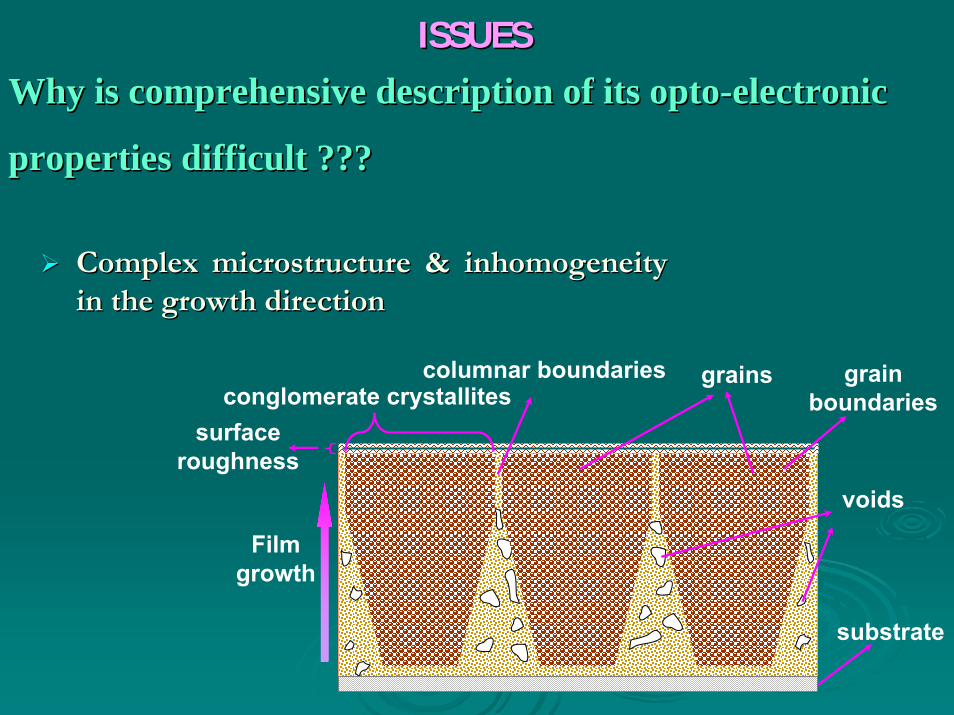
ISSUESISSUES
Electrical transport ???Electrical transport ???
Is it dominated by crystalline phase ???Is it dominated by crystalline phase ???oror
By interfacial regions between crystallites or grains???By interfacial regions between crystallites or grains???
A large number of studies claim that electronic A large number of studies claim that electronic transport in transport in μμcc--Si:H films is analogous to that Si:H films is analogous to that observed in aobserved in a--Si:H filmsSi:H films
GOAL GOAL
To study the To study the optoopto--electronic properties of well electronic properties of well
characterized characterized μμcc--Si:H films Si:H films
Identify the role of microstructure in determining Identify the role of microstructure in determining the electrical transport behaviorthe electrical transport behavior
ISSUESISSUES

Sample preparationSample preparation
Parallel-plate glow discharge plasma deposition system
R=1/1R=1/1 R=1/5R=1/5 R=1/10R=1/10
Substrate: Corning 1773
High purity feed gases:SiF4 , Ar & H2
Rf frequency 13.56 MHz
Silane flow ratio (R)= SiF4/H2
Thickness seriesTs=200 oC
μc-Si:Hfilm
R F
HSi SiNSi N
HSiH
HHN
N
H H
HHH
P E C V DR F
HSi SiNSi N
HSiH
HHN
N
H H
HHH
P E C V D
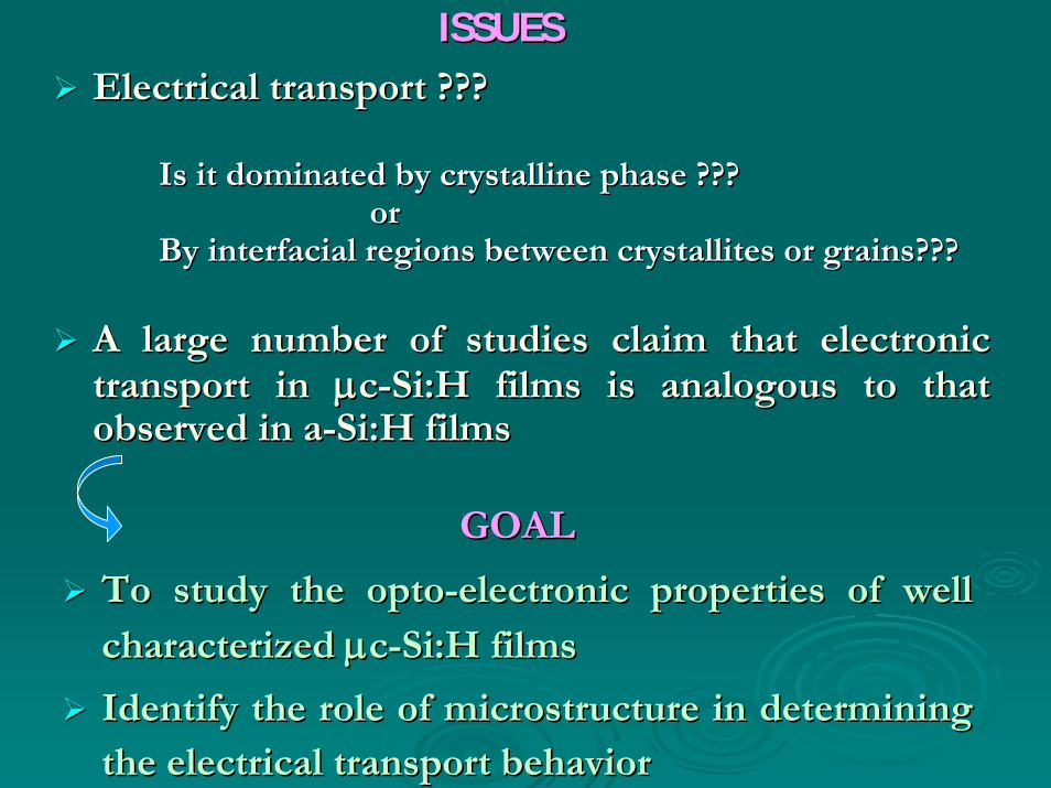
Film characterization
Structural Properties Electrical Properties
Xray Diffraction
Raman Scattering
In-situ Spectroscopy Ellipsometry
Atomic Force Microscopy
σd(T) measurement15K≤T ≤ 450K
σPh(T,∅) measurement15K≤T ≤ 325K
CPM measurement
Hall effect
TRMC

Raman ScatteringRaman Scattering
400 450 500 550 600
μc-Si (X, SiF4) μc-Si Std.
c-Si
Inte
nsity
(a.u
.)
Raman shift (cm-1)
450 475 500 525 5500.40.81.21.62.02.42.83.2 Layer sideR (SiF4 / H2) = 1/10
t=950 nm
t=590 nm
t=422 nm
t=390 nm
t=170 nm FB22GF
FB11GF
F281GF
FB23GF
FB04GF
F152GBt=52 nm
Inte
nsity
(arb
. uni
t)
Raman Shift (cm-1)
Effect of thickness variation

Spectroscopy Spectroscopy ellipsometeryellipsometery studystudy
1.5 2.0 2.5 3.0 3.5 4.0 4.5 5.0-10
-505
1015202530354045
F0E31 Fit a-Si:H c-Si
<ε2>
Energy (eV)2.5 3.0 3.5 4.0 4.5 5.00
5
10
15
20
25 B23 (R=10, t=590 nm) B11 (R=10, t=390 nm) B22 (R=10, t=170 nm) F152(R=10, t=55 nm) F16 (R=20, t=35 nm)
Energy (eV)
< ε 2 >
Fig. Measured <ε2> spectrum for the µc-Si:H samples. The sample name, thickness and its 1/R value are shown in the graph.

XX--ray diffraction studyray diffraction study
20 30 40 50 60 700
500
1000
1500
2000
2500
3000
3500
4000
4500
1/1
1/5
1/10
1.2 µm
1.1 µm
0.95 µm
(400)
(311)(220)
(111)
Cu Kα 2θ (degrees)
Inte
nsity
(a.u
.)
XRD study to see the effect of R (H2/SiF4)
Film deposited at SiF4/H2
flow ratio 1/1 shows a preferred orientation of (400).
film deposited at SiF4/H2
flow ratio of 1/5 shows a preferred orientation in (220)direction.
These results demonstrate the effectiveness of using fluorine based precursors in controlling the orientation of polycrystalline films on insulating glass substrates.
R

Structural FindingsStructural Findings
R =1/1
R =1/5
R =1/10
Random Orientation
(220) orientation
(400) orientation
Individual grains are bigger
Smooth top layerTightly packed
More Void fraction
Good crystallinity at bottom interface

Classification from coplanar electrical Classification from coplanar electrical transport point of viewtransport point of view
TYPE-A
TYPE-B
TYPE-C
More amorphous tissueSmall grains
Moderate amorphous tissueSmall grains
Tightly packed columnar crystalsLess amorphous tissueBig grains
Thickness (50-250 nm)
Thickness (300-600 nm)
Thickness (900-1200 nm)

SSPC Process
absorption of photons and generation of free electron-hole pairs
recombination of excess free electrons and holes through recombination centers
transport of mobile carriers
We have measured temperature and light intensity We have measured temperature and light intensity dependent steady state photoconductivity (SSPC) dependent steady state photoconductivity (SSPC) for the samples of different microstructurefor the samples of different microstructure

γγ is a measure of characteristic width of tail states nearer to is a measure of characteristic width of tail states nearer to EEff
According to the Rose model: According to the Rose model: the exponentially distributed tail state shows: the exponentially distributed tail state shows: γγ = = kTkTCC/(kT+kT/(kT+kTCC))
In amorphous semiconductor 0.5<In amorphous semiconductor 0.5<γγ <1.0<1.0γγ=0.5 bimolecular recombination kinetics=0.5 bimolecular recombination kineticsγγ=1 monomolecular recombination=1 monomolecular recombination
Significance of Significance of γγ
In a disordered material: In a disordered material:
σσphph ((TT, , φφ)=)=ee[[μμnn((nn--nn00) ) + + μμpp((pp--pp00)])]
Light Intensity dependence:Light Intensity dependence:
where, Gwhere, GLL = = φφ (1(1--R)[1R)[1--exp(exp(--ααd)]/dd)]/d
γσ Lph G∝
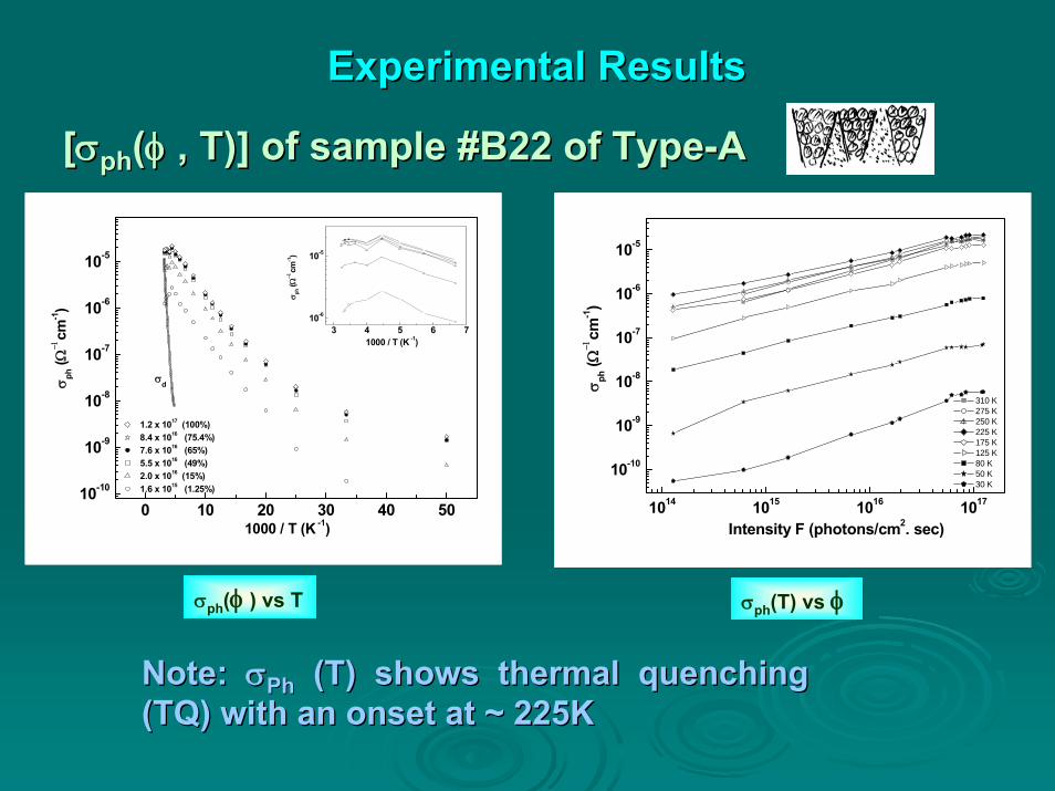
Experimental ResultsExperimental Results
[[σσphph((φφ , T)] of sample #B22 of Type, T)] of sample #B22 of Type--AA
0 10 20 30 40 5010-10
10-9
10-8
10-7
10-6
10-5
3 4 5 6 710-6
10-5
σd
1000 / T (K -1)
σ ph (Ω
−1cm
-1)
1.2 x 10¹⁷ (100%) 8.4 x 10¹⁶ (75.4%) 7.6 x 10¹⁶ (65%) 5.5 x 10¹⁶ (49%) 2.0 x 10¹⁶ (15%) 1.6 x 10¹⁵ (1.25%)
1000 / T (K -1)
σ ph (Ω
−1cm
-1)
1014 1015 1016 1017
10-10
10-9
10-8
10-7
10-6
10-5
σ ph (Ω
−1cm
-1)
Intensity F (photons/cm2. sec)
310 K 275 K 250 K 225 K 175 K 125 K 80 K 50 K 30 K
Note: Note: σσPhPh (T) shows thermal quenching (T) shows thermal quenching (TQ) with an onset at ~ 225K(TQ) with an onset at ~ 225K
σph(T) vs φσph(φ ) vs T

Experimental ResultsExperimental Results
[[σσphph((φφ , T)] of sample #B23 of Type, T)] of sample #B23 of Type--BB
Note: Note: σσPhPh (T) shows NO TQ(T) shows NO TQ
4 8 12 16 2010-12
10-10
10-8
10-6
10-4
σd
1000 / T (K -1)
σ ph (Ω
−1cm
-1)
Φ ( photons/cm2-sec ) 1x10¹⁴
1x10¹⁶
5x10¹⁶
1017
1012 1013 1014 1015 1016 1017
10-11
10-9
10-7
10-5
σ ph (Ω
−1cm
-1)
Φ (Photons/cm2-sec)
324 K 300 K 275 K 250 K 225 K 200 K 175 K 153 K 128 K 101 K 72 K 60 K 50 K 25 K
σph(φ ) vs T σph(T) vs φ
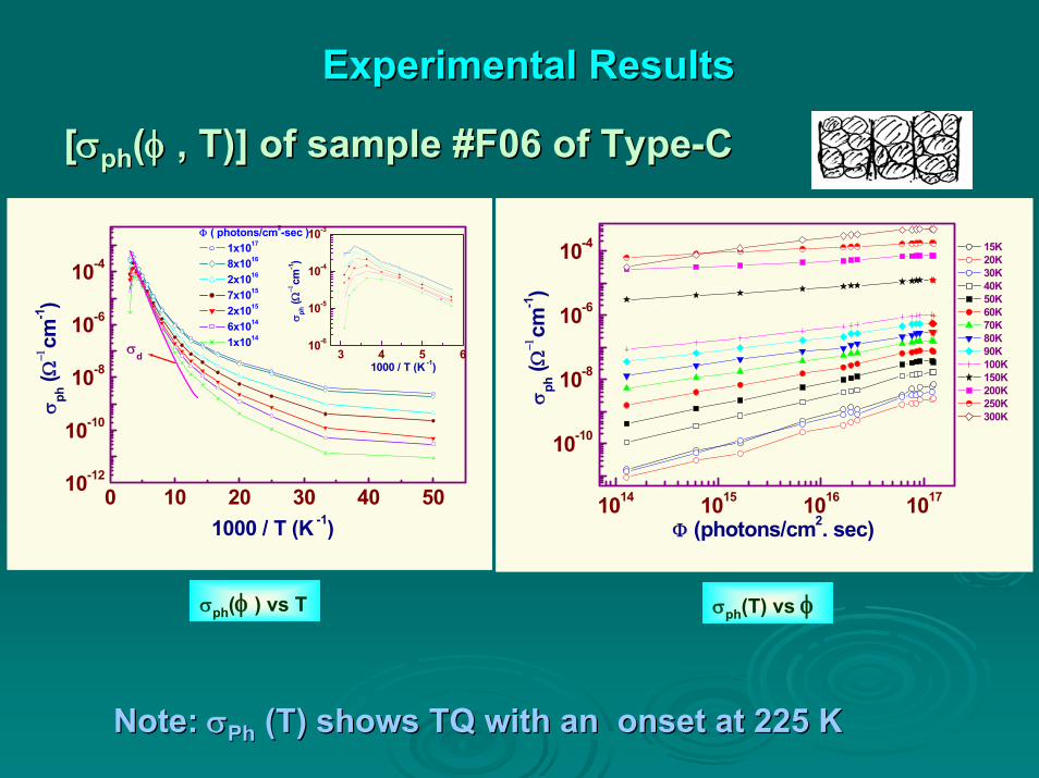
Experimental ResultsExperimental Results
[[σσphph((φφ , T)] of sample #F06 of Type, T)] of sample #F06 of Type--CC
Note: Note: σσPhPh (T) shows TQ with an onset at 225 K(T) shows TQ with an onset at 225 K
0 10 20 30 40 5010-12
10-10
10-8
10-6
10-4
3 4 5 610-6
10-5
10-4
10-3
1000 / T (K -1)
σ ph (Ω
−1cm
-1)
σd
Φ ( photons/cm2-sec ) 1x10¹⁷
8x10¹⁶
2x10¹⁶
7x10¹⁵
2x10¹⁵
6x10¹⁴
1x10¹⁴
σ ph (Ω
−1cm
-1)
1000 / T (K -1)
1014 1015 1016 1017
10-10
10-8
10-6
10-4
σ ph (Ω
−1cm
-1)
Φ (photons/cm2. sec)
15K 20K 30K 40K 50K 60K 70K 80K 90K 100K 150K 200K 250K 300K
σph(φ ) vs T σph(T) vs φ

0 10 20 30 40 50 60 70
0.2
0.4
0.6
0.8
1.0
γ
1000/T (K -1)
B22 F06 B23
temperature dependencies of light intensity exponent (γ)
Comparison of phototransport properties of all the three types of samples
TQ and 0.5<TQ and 0.5<γγ <1 : as <1 : as found in Typefound in Type--A: A:
NO TQ and 0.5<NO TQ and 0.5<γγ <1 : as <1 : as found in Typefound in Type--B: B:
TQ and TQ and γγ value value approaches to a lowest approaches to a lowest value of 0.14 at 225 K: as value of 0.14 at 225 K: as found in Typefound in Type--C: C:
Findings:Findings:
Qualitative analysisQualitative analysis
Causes of TQ :Causes of TQ :
The transformation of the recombination traffic The transformation of the recombination traffic from VBT states to DBfrom VBT states to DB
The asymmetry in band tails in the gap.The asymmetry in band tails in the gap.
Low value of defect densities or increasing nLow value of defect densities or increasing n--type type doping level may shift the onset of TQ to higher T. doping level may shift the onset of TQ to higher T.
Causes of sublinear behavior of Causes of sublinear behavior of γγ (<0.5) (<0.5)
The saturation of recombination centersThe saturation of recombination centers
The shift of The shift of EEFF towards band edges in doped towards band edges in doped material.material.
DISCUSSIONDISCUSSION

Phototransport properties of TypePhototransport properties of Type--A (TQ and 0.5< A (TQ and 0.5< γγ<1)<1)
This type of behavior is usually observed in typical This type of behavior is usually observed in typical aa--Si:HSi:H
Rose model works and width of CBT is deduced (Rose model works and width of CBT is deduced (kTckTc ~ 30 meV )~ 30 meV )
Possible explanation for Possible explanation for ““No TQ and 0.5< No TQ and 0.5< γγ<1 <1 ““ as found inas found in
TypeType--BB
Symmetric band tailsSymmetric band tails
Usually observed in typical Usually observed in typical µµcc--Si:HSi:H
Rose model works and width of CBT is deduced (Rose model works and width of CBT is deduced (kTkTCC ~ 25~ 25--28 28
meV )meV )
According to According to BalbergBalberg et. al (Phys. Rev. B 69, 2004, 035203): a et. al (Phys. Rev. B 69, 2004, 035203): a
Gaussian type VBT to be responsible for such behaviorGaussian type VBT to be responsible for such behavior
Qualitative analysisQualitative analysis

Phototransport properties of TypePhototransport properties of Type--C (TQ and C (TQ and γγ<0.5)<0.5)
Possible explanations for TQ behavior in TypePossible explanations for TQ behavior in Type--C materialC material
Rose model does not hold forRose model does not hold for TypeType--C materialC material
DBs unlikely to cause TQDBs unlikely to cause TQ
Possibilities of asymmetric band tail states in this type of Possibilities of asymmetric band tail states in this type of materialmaterial
lower DOS near the CB edge, i.e. a steeper CBT than VBT lower DOS near the CB edge, i.e. a steeper CBT than VBT (supported by defect pool model)(supported by defect pool model)
The CPM measurement supports the fact The CPM measurement supports the fact kTkTCC<<<<kTkTVV
Qualitative analysisQualitative analysis
Possible explanation for sublinear behavior of Possible explanation for sublinear behavior of γγ (<0.5) in Type(<0.5) in Type--C C
In TypeIn Type--C material, EC material, EFF is found to be very close to is found to be very close to EcEc (E(ECC--EEFF ~ ~ 0.34 eV)0.34 eV)
In doped aIn doped a--Si:H when Si:H when kTckTc << << kTvkTv δδn n ≈≈ nn00 then Rose model then Rose model doesndoesn’’t hold (by C. Main t hold (by C. Main …….).)
γγ=T/=T/TvTv for low excitationfor low excitation
γγ= = TTc/c/TTvv at high excitationat high excitation
According to Polycrystalline Si model two different VBT is According to Polycrystalline Si model two different VBT is also possible; also possible;
A sharper shallow tail near the edgeA sharper shallow tail near the edge--> originating from grain boundary > originating from grain boundary defectsdefects
A less steeper deeper tail associated with the defects in columnA less steeper deeper tail associated with the defects in columnar ar boundary regions. boundary regions.
Capture cross section for the deeper tail is smaller than the shCapture cross section for the deeper tail is smaller than the shallower allower one. one.
Qualitative analysisQualitative analysis
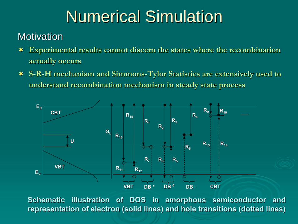
Numerical SimulationNumerical SimulationMotivationMotivation
Experimental results cannot discern the states where the recombiExperimental results cannot discern the states where the recombination nation actually occursactually occurs
SS--RR--H mechanism and SimmonsH mechanism and Simmons--TylorTylor Statistics are extensively used to Statistics are extensively used to understand recombination mechanism in steady state processunderstand recombination mechanism in steady state process
RR11RR22
RR33
RR44
RR55
RR66
RR77 RR88
RR1212
RR99
RR1111
RR1616
RR1515
RR1313
RR1010
RR1414
GGLL
EEVV
EECC
UU
VBTVBT CBTCBTDB DB ++ DB DB 00 DB DB --
VBTVBT
CBTCBT
Schematic illustration of DOS in amorphous semiconductor and Schematic illustration of DOS in amorphous semiconductor and representation of electron (solid lines) and hole transitions (drepresentation of electron (solid lines) and hole transitions (dotted lines)otted lines)

[ ] [ ] ( ) ( )[ ] ( ) ( )[ ] ( ) 022,,,, 000000000 =−−++−−−+−−− −−
DBDBDBDBDBVTVTCTCT FFFFNpnQpnQpnQpnQppnn
DBVTCTL UUUG ++=
Charge neutrality equationCharge neutrality equation
Recombination equationRecombination equation
( ) ( ) ( )pnQdEEFENQ CTCT
E
ECTCT
C
V
,=∫=
( ) ( )[ ] ( )pnQdEEFENQ VTVT
E
EVTVT
C
V
,1 =−∫=
( ) ( ) ( )−− −−+=− DBDBDBDBDBDBDB FFFFNpnQpnQ 22,, 00000
( ) ( ) ( )[ ]dEFFSFSFnENU nDBnDBnDBnDB
E
EDBDB
C
V
−−++ +−+∫= εε 0000
( ) ( ) ( )''
'
ppSnnSpSnS
EF CTp
CTn
CTp
CTn
CT +++
+=
( ) ( ) ( )''
'
ppSnnSpSnS
EF VTp
VTn
VTp
VTn
VT +++
+=

CBT
VBT
DB
( )( )( )
( )( )⎥⎥⎥⎥⎥
⎦
⎤
⎢⎢⎢⎢⎢
⎣
⎡
⎥⎦
⎤⎢⎣
⎡ −−−+
⎥⎦
⎤⎢⎣
⎡ −−−
×⎥⎦
⎤⎢⎣
⎡ −−×=
2
1
2
1
1
011
exp1
expexp
c
tcc
c
tcc
c
cctct
kTEEE
kTEEE
kTEENN
( )( )( )
( )( )⎥⎥⎥⎥⎥
⎦
⎤
⎢⎢⎢⎢⎢
⎣
⎡
⎥⎦
⎤⎢⎣
⎡ +−−+
⎥⎦
⎤⎢⎣
⎡ +−−
×⎥⎦
⎤⎢⎣
⎡ −−×=
2
1
2
1
1
011
exp1
expexp
v
tvv
v
tvv
v
vvtvt
kTEEE
kTEEE
kTEE
NN
( )( )
( )⎥⎦
⎤⎢⎣
⎡ −= 2
2
2/1 2exp
2 WEE
WNEN DBD
DB π

Steps in Numerical SimulationSteps in Numerical Simulation
DOS distribution is first assumedDOS distribution is first assumed
Guess values of n and p are givenGuess values of n and p are given
Charge neutrality equation & recombination rates equation Charge neutrality equation & recombination rates equation
are simultaneously solved for a fixed value of T and Gare simultaneously solved for a fixed value of T and GLL
SS--RR--H mechanism and SimmonsH mechanism and Simmons--TylorTylor Statistics are appliedStatistics are applied
NewtonNewton--RaphsonRaphson method for finding roots of n and pmethod for finding roots of n and p
SimpsonSimpson’’s method for numerical integrations method for numerical integration
n and p are obtainedn and p are obtained
We calculatedWe calculated σσphph ((TT, , φφ)=)=ee[[μμnn((nn--nn0) 0) + + μμpp((pp--pp0)]0)]
The corresponding The corresponding γγ values are obtained as in experimental values are obtained as in experimental
casecase

4 6 8 10
10-6
10-5
10-4
1000/T (K -1)
σ ph (Ω
-1cm
-1)
G=1019 cm-3sec-1
G=1020 cm-3sec-1
G=1021 cm-3sec-1
4 6 8 100.3
0.4
0.5
0.6
1000/T (K -1)
γ
γ
100 150 200 250 3001011
1013
1015
1017
1019R
ecom
bina
tion
rate
s (c
m-3se
c-1)
T (K)
Uct1 Uvt1 Uvt2 UDB
0.0 0.3 0.6 0.9 1.2 1.5 1.81013
1015
1017
1019
1021
DO
S (c
m-3eV
-1 )
EC- EF=0.34 eV
DB
CBT
VBT2
VBT1
ECEV
(E-EV) eV
Simulation results for Type-C material (ex. #F06)
μμnn = 10 = 10 cmcm22VV--11ss--11
μμpp == 0.5 0.5 cmcm22VV--11ss--11

Simulation results for Type-B material (#B23)
0.0 0.3 0.6 0.9 1.2 1.5 1.81013
1015
1017
1019
1021
DB
EC- EF=0.42 eV
CBT2
CBT1
VBT2
VBT1
DO
S (c
m-3eV
-1 )
EV EC(E-EV) eV4 6 8 1010-8
10-7
10-6
10-5
1000/T (K -1)
σ ph (Ω
-1cm
-1)
G=1018 cm-3sec-1
G=1019 cm-3sec-1
G=1020 cm-3sec-1
G=1021 cm-3sec-1
4 8 12 16 200.5
0.6
0.7
0.8
0.9
γ
γ
1000/T (K -1)100 150 200 250 3001011
1013
1015
1017
1019
T (K)
Rec
ombi
natio
n ra
tes
(cm
-3se
c-1)
Uct1 U
ct2 Uvt1 Uvt2 UDB
μμnn = 10 = 10 cmcm22VV--11ss--11
μμpp == 0.5 0.5 cmcm22VV--11ss--11

SummarySummaryThe qualitative as well as quantitative analysis of the The qualitative as well as quantitative analysis of the
study of our phototransport properties of undoped study of our phototransport properties of undoped µµcc--
Si:H thin films are in good agreement Si:H thin films are in good agreement
MicroMicro--structural differences leads to totally different structural differences leads to totally different
phototransport behavior. phototransport behavior.
The recombination rate of deeper valence band tail is The recombination rate of deeper valence band tail is
higher in percolated grains than in unpercolated grainshigher in percolated grains than in unpercolated grains
We propose different effective DOS distribution forWe propose different effective DOS distribution for
micromicro--structurally different structurally different μμcc--Si:H thin filmsSi:H thin films

![MICROCRYSTALLINE WAX - ::krishna::krishna.nic.in/PDFfiles/MSME/Chemical/MICROCRYSTALLINE WAX[1].pdf · Specification of Microcrystalline wax ... MRF Ltd. 1.000 43372 ... The content](https://img.pdfslide.us/doc/110x75/5aa76b097f8b9ac5648c1342/microcrystalline-wax-krishna-wax1pdfspecification-of-microcrystalline-wax.jpg)