Embed Size (px)
Citation preview

A quantitative numerical model of multilayer vapor-deposited organic light emittingdiodesJ. Staudigel, M. Stößel, F. Steuber, and J. Simmerer Citation: Journal of Applied Physics 86, 3895 (1999); doi: 10.1063/1.371306 View online: http://dx.doi.org/10.1063/1.371306 View Table of Contents: http://scitation.aip.org/content/aip/journal/jap/86/7?ver=pdfcov Published by the AIP Publishing Articles you may be interested in Simulation of charge injection enhancements in organic light-emitting diodes Appl. Phys. Lett. 79, 4438 (2001); 10.1063/1.1426683 Recombination efficiency in organic single-layer light-emitting diodes at high fields Appl. Phys. Lett. 79, 2529 (2001); 10.1063/1.1410339 Transient and steady-state behavior of space charges in multilayer organic light-emitting diodes J. Appl. Phys. 89, 4575 (2001); 10.1063/1.1352027 Numerical model for organic light-emitting diodes J. Appl. Phys. 89, 430 (2001); 10.1063/1.1327286 Erratum: “Efficiency peaks in the transient electroluminescence of multilayer organic light-emitting devices” [Appl.Phys. Lett. 76, 2170 (2000)] Appl. Phys. Lett. 77, 1560 (2000); 10.1063/1.1308052
[This article is copyrighted as indicated in the article. Reuse of AIP content is subject to the terms at: http://scitation.aip.org/termsconditions. Downloaded to ] IP:
14.139.194.12 On: Sun, 09 Nov 2014 17:37:16
A quantitative numerical model of multilayer vapor-deposited organic lightemitting diodes
J. Staudigela)
Siemens AG, Corporate Technology, ZT MF 1, Paul-Gossen-Strasse 100, D-91052 Erlangenand Universita¨t Erlangen-Nu¨rnberg, Institut fur Angewandte Physik, D-91058 Erlangen, Germany
M. Stoßel and F. SteuberSiemens AG, Corporate Technology, ZT MF 1, Paul-Gossen-Strasse 100, D-91052 Erlangenand Universita¨t Erlangen-Nu¨rnberg, Institut fur Werkstoffwissenschaften VI, D-91058 Erlangen, Germany
J. SimmererSiemens AG, Corporate Technology, ZT MF 1, Paul-Gossen-Strasse 100, D-91052 Erlangen, Germany
~Received 22 February 1999; accepted for publication 8 June 1999!
A one-dimensional numerical model for the quantitative simulation of multilayer organic lightemitting diodes ~OLEDs! is presented. It encompasses bipolar charge carrier drift withfield-dependent mobilities and space charge effects, charge carrier diffusion, trapping, bulk andinterface recombination, singlet exciton diffusion and quenching effects. Using field-dependentmobility data measured on unipolar single layer devices, reported energetic levels of highestoccupied and lowest unoccupied molecular orbitals, and realistic assumptions for experimentally notdirect accessible parameters, current density and luminance of state-of-the-art undopedvapor-deposited two- and three-layer OLEDs with maximum luminance exceeding 10000 cd/m2
were successfully simulated over 4 orders of magnitude. For an adequate description of thesemultilayer OLEDs with energetic barriers at interfaces between two adjacent organic layers, themodel also includes a simple theory of charge carrier barrier crossing and recombination at organic–organic interfaces. The discrete nature of amorphous molecular organic solids is reflected in themodel by a spatial discretization according to actual molecule monolayers, with hopping processesfor charge carrier and energy transport between neighboring monolayers. ©1999 AmericanInstitute of Physics.@S0021-8979~99!02218-5#
I. INTRODUCTION
Ever since the first appearances of efficient organic lightemitting diodes~OLEDs!,1–4 their properties and the mecha-nisms of the physical processes involved were subject to ana-lytical and numerical investigation. Basic understanding ofOLED properties still remains a crucial point for the devel-opment of highly efficient devices, which meet the require-ment specifications of typical target applications.
Several theoretical models for OLEDs have been pro-posed in the past, each starting from different assumptions tosimplify the complex interplay of mechanisms involved. Dueto the large variety of known OLED setups, suitable materi-als, and mechanisms governing their behavior, distinct mod-els were developed to explain the experimental findings.5–17
The proposed models comprise injection limited currentflow,5,6,9 the transition from injection to bulk limitation,7,10,13
and purely space charge limited current~SCLC!flow,11,12,15,16either on monolayer5,9,12–17or multilayer6–8,11
devices.The present article comprises the numerical modeling of
undoped multilayer vapor-deposited OLEDs based on smallfunctional molecules. For this purpose, a numerical ratherthan an analytical model was chosen for an adequate imple-mentation of the discrete nature of the amorphous molecular
organic solids. The simulation results are compared with ex-perimental data in order to gain further insight into themechanisms governing the behavior of our processedOLEDs, with special respect to the implications for deviceoptimization.
In Sec. III, we will present dark current transients ofhole- and electron-only single layer samples which, in addi-tion to a quantitative agreement between measured steadystate current densities and predictions from space charge lim-ited current theory, prove space charge limitation of the cur-rent flow.18 Thus, the assumption of ohmic contacts both forhole and electron injection in our OLED model, which willbe presented in detail in Sec. II, is experimentally verified.
The electro-optical characteristics of our undoped vapor-deposited two- and three-layer OLEDs showing a maximumluminance of more than 10 000 cd/m2, were successfullysimulated over 4 orders of magnitude in current density andluminance. Starting from measured field-dependent electronand hole mobilities~which were derived from our own ex-perimental data based on the evaluation of transient SCLCpeaks18!, reported data on energetic levels of lowest unoccu-pied and highest occuppied molecular orbitals~LUMOs,HOMOs!,19 and realistic assumptions for experimentally notdirect accessible parameters, we will deduce the built-in po-tential, average trap depths and trap concentrations of ourprocessed two-layer devices by a comparison of simulateda!Electronic mail: [email protected]
JOURNAL OF APPLIED PHYSICS VOLUME 86, NUMBER 7 1 OCTOBER 1999
38950021-8979/99/86(7)/3895/16/$15.00 © 1999 American Institute of Physics
[This article is copyrighted as indicated in the article. Reuse of AIP content is subject to the terms at: http://scitation.aip.org/termsconditions. Downloaded to ] IP:
14.139.194.12 On: Sun, 09 Nov 2014 17:37:16
and measured current densities in Sec. III. The energetic dis-order parameter at the interface between hole transport layer~HTL! and electron transport layer~ETL!, which governs theprobability of bulk exciton formation from interface recom-bination, is then derived from the comparison of simulatedand measured luminance data.
The experimentally observed improvements in theelectro-optical characteristics from two- to three-layer de-vices ~the latter comprising an additional HTL!, such as re-duced current density and enhanced luminance, can then beunderstood in terms of different charge carrier accumulationzones arising from different energetic barriers for charge car-riers at the organic–organic interfaces. Detailed spatial dis-tributions of electric field, charge carrier densities and singletexciton density inside the organic layers, which will be dis-cussed in Sec. IV, yield new physical insight into the differ-ent mechanisms governing the properties of state-of-the-arttwo- and three-layer devices.
II. THE MODEL
Most models for the simulation of OLEDs start with theimplicit or explicit assumption of a spatially continuous dis-tribution of the variables of state.6–17 In those cases where noanalytic solution for the steady state can be derived from thedifferential equation system used for describing the physicalprocesses, variables of state and equation system are onlydiscretized to gain numeric solutions for the steady state un-der given boundary conditions, with no direct size and posi-tion relation between supporting points and molecules.13–16
In this paper, we will choose a different approach whichpartly reflects the discrete nature of amorphous molecularorganic thin films, since the diameters of commonly usedorganic molecules are only between one and two orders ofmagnitude smaller than actual layer thicknesses.
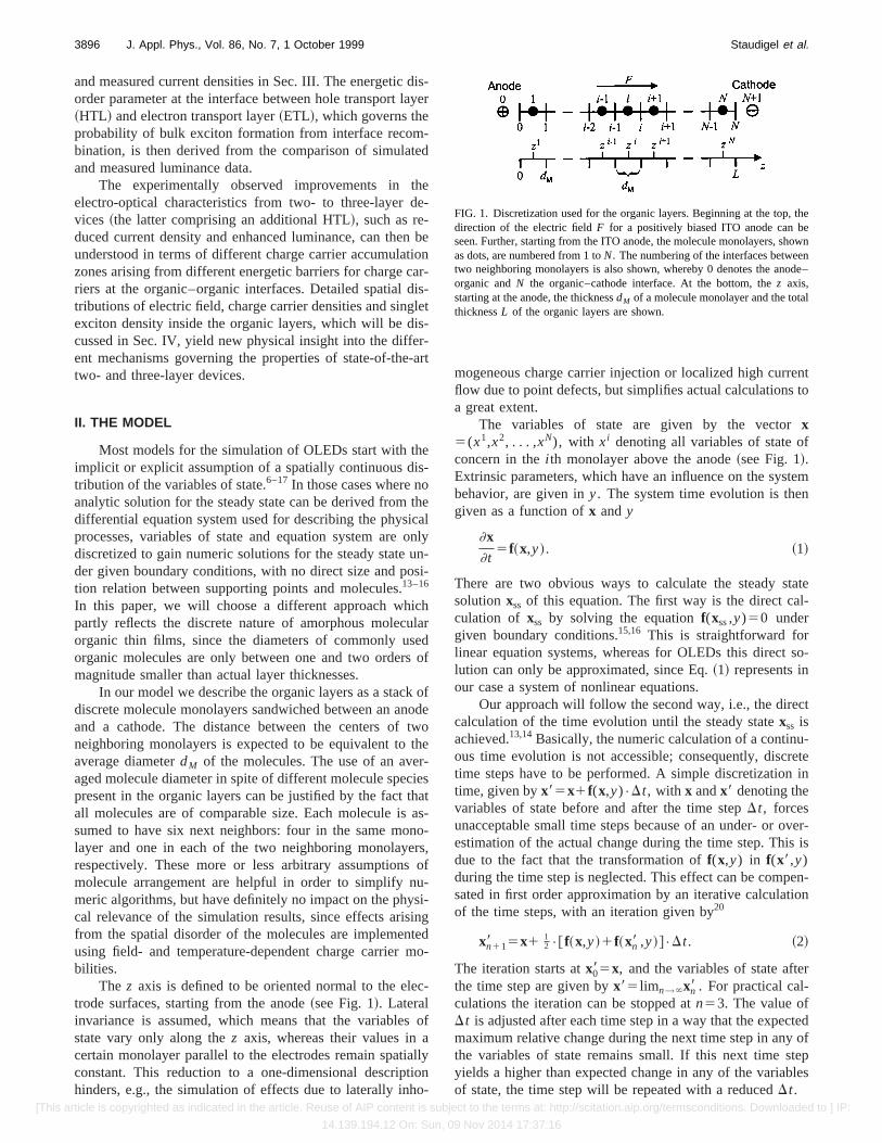
In our model we describe the organic layers as a stack ofdiscrete molecule monolayers sandwiched between an anodeand a cathode. The distance between the centers of twoneighboring monolayers is expected to be equivalent to theaverage diameterdM of the molecules. The use of an aver-aged molecule diameter in spite of different molecule speciespresent in the organic layers can be justified by the fact thatall molecules are of comparable size. Each molecule is as-sumed to have six next neighbors: four in the same mono-layer and one in each of the two neighboring monolayers,respectively. These more or less arbitrary assumptions ofmolecule arrangement are helpful in order to simplify nu-meric algorithms, but have definitely no impact on the physi-cal relevance of the simulation results, since effects arisingfrom the spatial disorder of the molecules are implementedusing field- and temperature-dependent charge carrier mo-bilities.
The z axis is defined to be oriented normal to the elec-trode surfaces, starting from the anode~see Fig. 1!. Lateralinvariance is assumed, which means that the variables ofstate vary only along thez axis, whereas their values in acertain monolayer parallel to the electrodes remain spatiallyconstant. This reduction to a one-dimensional descriptionhinders, e.g., the simulation of effects due to laterally inho-
mogeneous charge carrier injection or localized high currentflow due to point defects, but simplifies actual calculations toa great extent.
The variables of state are given by the vectorx5(x1,x2, . . . ,xN), with xi denoting all variables of state ofconcern in thei th monolayer above the anode~see Fig. 1!.Extrinsic parameters, which have an influence on the systembehavior, are given iny. The system time evolution is thengiven as a function ofx andy
]x
]t5f~x,y!. ~1!
There are two obvious ways to calculate the steady statesolutionxss of this equation. The first way is the direct cal-culation of xss by solving the equationf(xss,y)50 undergiven boundary conditions.15,16 This is straightforward forlinear equation systems, whereas for OLEDs this direct so-lution can only be approximated, since Eq.~1! represents inour case a system of nonlinear equations.
Our approach will follow the second way, i.e., the directcalculation of the time evolution until the steady statexss isachieved.13,14Basically, the numeric calculation of a continu-ous time evolution is not accessible; consequently, discretetime steps have to be performed. A simple discretization intime, given byx85x1f(x,y)•Dt, with x andx8 denoting thevariables of state before and after the time stepDt, forcesunacceptable small time steps because of an under- or over-estimation of the actual change during the time step. This isdue to the fact that the transformation off(x,y) in f(x8,y)during the time step is neglected. This effect can be compen-sated in first order approximation by an iterative calculationof the time steps, with an iteration given by20
xn118 5x1 12 •@ f~x,y!1f~xn8 ,y!#•Dt. ~2!
The iteration starts atx085x, and the variables of state afterthe time step are given byx85 limn→`xn8 . For practical cal-culations the iteration can be stopped atn53. The value ofDt is adjusted after each time step in a way that the expectedmaximum relative change during the next time step in any ofthe variables of state remains small. If this next time stepyields a higher than expected change in any of the variablesof state, the time step will be repeated with a reducedDt.
FIG. 1. Discretization used for the organic layers. Beginning at the top, thedirection of the electric fieldF for a positively biased ITO anode can beseen. Further, starting from the ITO anode, the molecule monolayers, shownas dots, are numbered from 1 toN. The numbering of the interfaces betweentwo neighboring monolayers is also shown, whereby 0 denotes the anode–organic andN the organic–cathode interface. At the bottom, thez axis,starting at the anode, the thicknessdM of a molecule monolayer and the totalthicknessL of the organic layers are shown.
3896 J. Appl. Phys., Vol. 86, No. 7, 1 October 1999 Staudigel et al.
[This article is copyrighted as indicated in the article. Reuse of AIP content is subject to the terms at: http://scitation.aip.org/termsconditions. Downloaded to ] IP:
14.139.194.12 On: Sun, 09 Nov 2014 17:37:16
In the following the variables of statex and their pro-posed change during a time stepDx5f(x,y)•Dt will beidentified with variables of state and corresponding processesin OLEDs. The result will be a nonlinear equation system,which is of the same type as an equation system obtainedfrom a spatial and temporal discretization of a second orderpartial differential equation system. In normal cases suchequation systems, including drift and diffusion terms, needboundary conditions to ensure that the obtained solutions areindependent of the chosen discretization. In our special case,however, there exists a self-regulation mechanism, namelythe decrease of the electric field at the electrodes~causing adecrease of the charge carrier injection! due to space chargesin the bulk material. This self-regulation allows, in combina-tion with the fixed spatial discretization in molecule mono-layers, the reduction of the boundary condition problem to aninitial value problem, namely the state of the system at thebeginning, making the calculation of the time evolution awhole lot easier.
In Secs. II A–II L the model will be presented in detail.Sections II B–II I refer to the mechanisms governing theelectronic characteristics of OLEDs, whereas the implemen-tation of the optical characteristics will be outlined in Secs.II J and II K.
A. Variables of state
The total amount of charge carriers in a real device isdivided into free and trapped charge carriers in our OLEDmodel.11,13,15 Free charge carriers are expected to have anaverage mobility equivalent to the mobilities obtained fromdark current transients.18 Trapping of charge carriers is as-sumed to occur either due to structural disorder orimpurities.12
For an adequate description of OLED behavior consid-ering these assumptions, the variables of statex must at leastcomprise the free and trapped hole densitiespf and pt , thefree and trapped electron densitiesnf andnt , and the singletexciton concentrations. pf
i , pti , nf
i , nti , and si denote the
according densities in thei th monolayer above the anode.Triplet excitons are not expected to be of any major influ-ence on device properties, which includes the neglect oftriplet–triplet annihilation processes.21
The extrinsic parametersy are given by the applied volt-ageV and the temperatureT.
B. The electric field
The applied voltageV causes the existence of an electricfield in the organic layers. The average electric fieldF for atotal layer thicknessL is given by
F5V2Vbi
L, ~3!
whereVbi denotes the built-in potential due to different workfunctions of the electrode materials and possible dipole lay-ers at the electrode–organic interfaces. The voltageV is de-fined to be positive for a positively biased anode.
Free and trapped charge carriers in OLEDs consisting ofthe later on mentioned organic materials~see Fig. 4! are to a
major extent excess charge carriers, so that their influence onthe local electric fieldFi in the i th monolayer has to beconsidered. The electric fieldF if
i at the interface between twoadjacent monolayers~see Fig. 1! must consider all excesscharges, given by the excess charge density
% i5e•@~pfi 2pf ,0
i !1~pti2pt,0
i !2~nfi 2nf ,0
i !2~nti2nt,0
i !#, ~4!
with the elementary chargee and the intrinsic free andtrapped charge carrier densitiespf ,0
i , pt,0i , nf ,0
i , andnt,0i , in
the organic monolayers below and above:
F ifi 5
dM
2«0F (
j 51
i% j
« j 2 (j 5 i 11
N% j
« j G1r
««0. ~5!
«0 denotes the dielectric constant, while« i and « denote thelocal and the averaged relative dielectric constant. The elec-tric field in the i th organic layer is then given as the averagebetween the electric fields at the enclosing interfaces:
Fi5F if
i 211F ifi
2. ~6!
The anode surface charge densityr in Eq. ~5! is adjustedfor every time step to maintain the condition
(i 51
N
Fi•dM5V2Vbi , ~7!
which in other words means that space charges will be com-pensated by additional electrode surface charges to maintainthe total potential drop in the organic layers.
C. Charge carrier drift
The local electric field in the organic layers is respon-sible for the drift of the free charge carriers. In amorphousmolecular organic solids such transport phenomena are com-monly described as hopping processes. Holes are transportedin the HOMOs, whereas electrons are transported in the LU-MOs.
Such hopping processes occur randomly and must there-fore be described on a microscopic level using Monte Carlomethods.22 Nevertheless, for a huge amount of hopping pro-cesses, in our case from one monolayer to the neighboringmonolayers, statistics allow the use of average parametersdescribing the hopping processes.22 This averaging of themicroscopic charge carrier mobility distribution leads to anondispersive description of the charge carrier transport.Nondispersive charge carrier transport has been observed fortypical electric fields during OLED operation in the hole andelectron transporting materials which are investigated in oursimulation and experimental work, thus justifying thissimplification.23,24 All the following formulas for the trans-port mechanisms will therefore use average parameters. Therelations will be given for holes only, since the formulas forelectrons have equivalent forms.
The average waiting timetpi between two consecutive
hopping processes~for a molecule arrangement as describedabove! can be expressed as the quotient between the jump
3897J. Appl. Phys., Vol. 86, No. 7, 1 October 1999 Staudigel et al.
[This article is copyrighted as indicated in the article. Reuse of AIP content is subject to the terms at: http://scitation.aip.org/termsconditions. Downloaded to ] IP:
14.139.194.12 On: Sun, 09 Nov 2014 17:37:16
distance, given as the molecule diameter, and the averagelocal charge carrier velocity of the molecule at the initialposition i
tpi 5
dM
mpi Fi . ~8!
The average local hole mobilitympi is a function of the local
electric field and of the temperatureT, as well as it is a directfunction of the positioni due to the stacking of differentorganic materials in multilayer OLEDs. As a simplification,the mobility corresponding to the molecule at the final posi-tion after the hopping process~either at positioni 21 or i11! is assumed not to have any influence on the averagewaiting time tp
i . All effects arising from the energetic andspatial disorder in organic solids are packed into the field andtemperature dependence of the charge carrier mobilities. Asuitable previously reported relation for this dependence willbe presented later on.22
The change of the free hole density in thei th monolayerdue to hopping processes from thei th into the (i 11)thmonolayer during the time stepDt is given by Dpdrift
i→ i 11
5Dt/ tpi•pf
i , where a substition oftpi according to Eq.~8!
yields the final form
Dpdrifti→ i 115H mp
i Fi
dMpf
i•Dt, Fi.0
0, Fi<0. ~9!
Dpdrifti→ i 21 is represented by an equivalent form. The total
change of the free hole density in thei th monolayer due tohopping processes results from the sum of all hopping pro-cesses involving this monolayer
Dpdrifti 5Dpdrift
i 21→ i2Dpdrifti→ i 211Dpdrift
i 11→ i2Dpdrifti→ i 11. ~10!
The total changeDndrifti of the free electron density can be
derived to an equivalent form to Eq.~10!.
D. Charge carrier diffusion
In addition to the charge carrier drift parallel to the di-rection of the electric field, a random charge carrier move-ment due to thermally stimulated hopping processes with nopreferential direction occurs. This free charge carrier diffu-sion can be described equivalently to Eq.~9!, however, byexcluding the direction limitation due to the electric field
Dpdiffi→ i 115
vdiff, pi
dMpf
i•Dt ~11!
Again, only the free hole density will be derived, since thefree electron diffusion is equivalent. The average local dif-fusion velocityvdiff, p
i can be obtained from the diffusion co-efficient Dp
i and the molecule diameter
vdiff, pi 5
Dpi
dM. ~12!
The Einstein relation between diffusion coefficient and fieldindependent charge carrier mobility18
Dp5mp•kBT
e, ~13!
with kB denoting the Boltzmann constant, is in this generalform not applicable for OLEDs. The observed increase in thecharge carrier mobility due to the electric field, arising fromthe lowering of the potential barrier for a hopping process,22
exists only in the drift direction, whereas in the reverse di-rection a decrease must be expected. Additionally, the elec-tric field itself decreases the probability of hopping processesagainst the drift direction, since the charge carriers gain po-tential energy according to the total potential differencealong the jump path, which is for typical electric fields andmolecule diameters in the order of magnitude ofkBT.
The above mentioned effects, which favor a diffusion inthe drift direction, will be partly considered in the model bya proposed diffusion mobility, defined as
mdiff, pi→ i 11~Fi !5H mp
i ~Fi !, Fi.0
mpi ~0!, Fi<0, ~14!
with mdiff, pi→ i 21(Fi) analogous to this definition. Using Eqs.
~11!, ~12!, and~13!, the change in the free hole density dueto thermally assisted jumps from thei th into the (i 11)thmonolayer can be expressed as
Dpdiffi→ i 115
mdiff, pi→ i 11~Fi !•kBT
e•dM2 pf
i•Dt, ~15!
with Dpdiffi→ i 21 having an analogous form. The total change of
the free hole density in thei th monolayer due to diffusioncan again be gained from the sum over all changes involvingthis monolayer
Dpdiffi 5Dpdiff
i 21→ i2Dpdiffi→ i 211Dpdiff
i 11→ i2Dpdiffi→ i 11. ~16!
The total change of the free electron densityDndiffi is equiva-
lent to Eq.~16!.A comparison of drift and diffusion velocities for typical
electric fields in OLEDs makes clear that the major part ofthe total charge carrier transport is governed by the chargecarrier drift.
E. Charge carrier injection
In our proposed OLED model the injecting contacts forholes and electrons are assumed to be ohmic, since currentlimitation due to barriers at the electrode–organic interfacesis not acceptable for high-performance OLEDs. Naturally,this condition has to be verified experimentally both for an-ode and cathode before starting the simulation~see Sec. III!.
Generally, an ideally injecting ohmic contact can beimplemented by a huge amount of charge carriers waiting atthe electrode–organic interfaces~position 0 for holes andN11 for electrons, see Fig. 1!. One possible description forthe change of the free hole density in the first monolayer is
Dpdrift0→15H mp
1F1
dMpanode•Dt, F1.0
0, F1<0, ~17!
wherepanodeshould be at least one order of magnitude largerthan the maximum of the hole density in the organic layers.The actual amount of injected holes is governed by the elec-tric field F1 in the first monolayer, which will be decreased
3898 J. Appl. Phys., Vol. 86, No. 7, 1 October 1999 Staudigel et al.
[This article is copyrighted as indicated in the article. Reuse of AIP content is subject to the terms at: http://scitation.aip.org/termsconditions. Downloaded to ] IP:
14.139.194.12 On: Sun, 09 Nov 2014 17:37:16
due to space charges~but will remain positive! and limitfurther charge injection. The electron injectionDndrift
N11→N atthe cathode is equivalent to Eq.~17!.
The diffusion of charge carriers from the electrodes intothe organic bulk material is not implemented. Argumentsshowing that this diffusion is not relevant can be derivedfrom the charge injection model proposed by Arkhipov andco-workers.10 In their model for charge injection in OLEDs,the number of charge carriers effectively entering the organicbulk is significantly reduced by the image potential causedby the charge carriers themselves, which forces the majorityof the carriers to jump back into the electrode after enteringthe first organic monolayer. The charge carriers are only ableto overcome the image potential in the presence of a positiveelectric field. The diffusion length of charge carriers from theelectrodes is therefore significantly reduced in comparison todiffusion lengths neglecting the image potential. The as-sumed absence of charge carrier diffusion from the elec-trodes into the adjacent organic layers is forced in the modelby Dpdiff
0→150 andDndiffN11→N50.
The control of the amount of injected charge carriersthrough the charge carriers present in the organic layers pro-vides an efficient controlling mechanism in the simulationfor a proper time evolution, thus making forced boundaryconditions not neccessary. One initial condition, preferablyan ‘‘empty’’ device without any excess charge carriers, issufficient to obtain physical relevant results as outlinedabove.
F. Bulk recombination
The recombination of holes and electrons to excitonsoccurs due to attractive Coulombic interaction between thetwo different charge carrier species. The change of the freehole and electron density during the time stepDt due to therecombination of the free charge carriers in thei th mono-layer can be described as
DRpfnf
i 5g•pfi nf
i•Dt, ~18!
whereg is the recombination coefficient in accordance withLangevin’s theory, which is known to be appropriate for dis-ordered organic systems25
g5e•~mp
i 1mni !
« i«0. ~19!
G. Charge carrier trapping
Charge carrier traps are states with energetic positions inbetween the energetic levels of the HOMO and the LUMO.Trap states may have various origins, e.g., material impuri-ties or structural disorder.12 The occupation of trap states,which are uncharged when empty, depends on the freecharge carrier densities and the trap depth, given as the en-ergetic distance of the trap state to the next transport site.
For shallow trap states arising from structural disorder inthe organic layers, recombination of free charge carriers withtrapped ones is assumed to be radiative with the same effi-ciency as for recombination in between free charge carriers.
The decrease of the free hole density, respectively theincrease of the trapped hole density, in thei th monolayerduring the time stepDt is given by
Dpti5Fmp
i•S uFi u1
kBT
e•dMD
vpi
G •s t•F pfi•~Nt,p
i 2pti !2pt
i
•~NHOMO2pfi
.NHOMO
!•expS 2Et,p
i
kBTD G •Dt. ~20!
The trap states are supposed to be not degenerated. The ve-locity vp
i of the holes in thei th monolayer is approximatedas the sum of the drift and diffusion velocity. The crosssection for charge carrier trappings t is estimated from thegeometric area occupied by a single molecule. Trapping issupposed to possibly occur on the regarded molecule itselfplus on its four next neighbors in the same monolayer, thusyielding the estimations t55•dM
2 .Equation~20! reflects that the trapping of holes is pro-
portional to the free hole density and to the concentration ofempty trapsNt,p
i 2pti . The detrapping, which is proportional
to the density of trapped holes and~to a good approximation!to the densityNHOMO of free states in the HOMO, occurs asa function of the trap depthEt,p
i only thermally activated.Considering every single molecule as a state, the density
of states in the HOMO can be approximated to
NHOMO5dM23, ~21!
which is essentially the density of molecules in organic sol-ids.
The presence of free electrons can significantly decreasethe number of trapped holes due to recombination processes.The decrease of the free electron density and of the trappedhole density due to recombination processes according toLangevin’s theory is given by
DRptnf
i 5e•mn
i
« i«0•pt
infi•Dt. ~22!
The density of trapped holespt,ssi in the steady state can
be derived from the conditionDpti2DRptnf
i 50 to
pt,ssi 5Nt,p
i•F 11
NHOMO
pfi •expS 2
Et,pi
kBTD
1
e•mni
« i«0•nf
i
s t•mpi•S uFi u1
kBT
e•dMD •pf
iG 21
. ~23!
The calculation of the time evolution can be stopped whenthe relative deviation between the actual and the steady statetrapped charge carrier densities becomes insignificant~<0.1% in our simulation!.
The formula given by Lampert and Mark18 for the uni-polar ~hole-only! case can be derived from Eq.~23! for nf
i
3899J. Appl. Phys., Vol. 86, No. 7, 1 October 1999 Staudigel et al.
[This article is copyrighted as indicated in the article. Reuse of AIP content is subject to the terms at: http://scitation.aip.org/termsconditions. Downloaded to ] IP:
14.139.194.12 On: Sun, 09 Nov 2014 17:37:16
50, that means in the absence of free electrons. The defini-tion of the commonly used quasi-Fermi level, given here forholes by18
EF,pi 5EHOMO
i 2kBT• ln~pfi /NHOMO!, ~24!
normally allows the description of the hole trap states occu-pation using a Fermi distribution.18 Due to the additionalrecombination term in Eq.~23!, however, this definitionmakes no sense in the bipolar case.EF,p
i as defined by Eq.~24! can then no longer be interpreted as the local Fermilevel which governs the occupation of the states.
For the trapping of electrons equivalent relations to theabove mentioned can be derived. Again, the definition of aquasi-Fermi levelEF,n for electrons makes no sense in thepresence of free holes. It is also possible to implement con-tinuous trap distributions by a discretization in single traplevels, where each trap level has to be treated separately.
H. Internal interfaces
Interfaces between two adjacent organic layers have amajor influence on current flow and device efficiency. Theactual processes at internal interfaces are not fully under-stood yet, so we will propose a simple model of the interfaceprocesses in the first step. In the following, the organic ma-terials are assumed not to interact directly. This means thatno particular surface states or charge-transfer complex for-mation are considered, since there is no experimental evi-dence for the existence of such states in electroluminescencespectra for the material combinations used.
In our vapor-deposited multilayer OLEDs the energeticlevels of the HOMO and of the LUMO, starting from theanode, decrease from organic layer to organic layer.19 There-fore, charge carriers have to ‘‘climb’’ a staircase on an en-ergetic scale before they reach the recombination zone. Eachinterface represents an energetic barrier, which has to becrossed by the free charge carriers. The height of such abarrier ~DEp for holes! is then given as the difference be-tween the energetic levels of the HOMOs of the two organiclayers~see Fig. 2!.
A hole arriving at the interface is assumed to have twoways to cross the interface. On one hand, it can perform athermally assisted jump over a~due to the potential drop inthe electric field! decreased energetic barrierDEp8 , which isproposed to be of the form
DEp85DEp2e•F j1F j 11
2•dM ~25!
~see dashed arrows in Fig. 2! or, on the other hand, recom-bine directly with an electron from the other side of the in-terface. The interface recombination, that means the decreaseof the hole density in thej th monolayer, which is equivalentto the decrease of the electron density in the (j 11)th mono-layer, is assumed to be similar to the bulk recombination,with the difference that holes and electrons are spatiallyseparated by the interface
DRp f n fif 5
e•~mpj 1mn
j 11!
««0•pf
j nfj 11
•Dt, ~26!
where « denotes the averaged relative dielectric constant inthese two monolayers.
For thermally assisted barrier crossing, the energetic dis-order of the density of states~DOS! has to be considered.The energetic disorder at the interface arises from a similareffect as the energetic disorder in the bulk, namely an inho-mogeneous broadening of the DOS due to interactions be-tween neighboring molecules,22 which may be superposed byan additional disorder due to the interdiffusion of the differ-ent molecule species.
The DOS in the interfacial monolayersj and j 11 areassumed to have a Gaussian shape distribution equivalent tothe energetic bulk disorder proposed by Ba¨ssler,22 given forholes by
G~E!5NHOMO
sA2p•expS 2
E2
2s2D , ~27!
with E denoting the energetic distance to the energetic posi-tion of the maximum of the DOS, ands denoting the ener-getic DOS width, which is assumed to be equal at both sidesof the interface.
The zero-field steady state value for the energetic dis-tance of energetically relaxed charge carriers to the maxi-mum in the DOS~given asEHOMO
i , respectively,ELUMOi )
after a large number of hopping processes can be calculatedto s2/kBT.22 Since the charge carriers gain an energy portioneFidM ~typically on the order ofkBT) during every hoppingprocess, that means they can enter the DOS in the nextmonolayer at a higher energy level, and since the number ofhopping processes needed to cross such thin layers is ratherlimited, the assumption of a totally relaxed zero-field occu-pation of the DOS cannot be justified in OLEDs. Instead, we
FIG. 2. Proposed barrier crossing and recombination processes at the inter-face between two different organic materials. Under the condition of ener-getic barriersDEp and DEn due to steps in the energetic positions of theHOMO and the LUMO at the interface, holes and electrons are, on onehand, able to cross the reduced energetic barriersDEp8 andDEn8 by a singlethermally stimulated hopping process~dashed arrows!, or, on the other hand,they recombine directly at the interface~dotted arrows!.
3900 J. Appl. Phys., Vol. 86, No. 7, 1 October 1999 Staudigel et al.
[This article is copyrighted as indicated in the article. Reuse of AIP content is subject to the terms at: http://scitation.aip.org/termsconditions. Downloaded to ] IP:
14.139.194.12 On: Sun, 09 Nov 2014 17:37:16
assume a homogeneous occupation of the DOS at the inter-face, reflecting an insufficient energetic relaxation of thecharge carriers within the DOS in the bulk.
The probability for a charge carrier to enter the neigh-boring DOS at a higher energetic level is assumed to bethermally activated, whereas a downward jump is assumed tooccur instantaneously.22 The total probability for a chargecarrier to cross an interface with a reduced energetic barrierDE8 is then given as
G~DE8!5c•E2`
`
dE G~E!E2`
`
dE8 G~E8!
•H expS 2E81DE82E
kBT D , E81DE8.E
1, E81DE8<EJ ,
~28!
with E andE8 denoting the energetic distance to the maxi-mum of the DOS before and after the interface~defined bythe charge carrier jump direction!. The constantc, whichdepends only ons, is given by the conditionG(0)51. In thecase of a negative barrier in jump direction,G(DE8) is set toone. In Fig. 3, the dependence of the probabilityG on theenergetic barrier height is plotted for different values of theenergetic disorders. Equation~28! is only applicable as longas the occupation of the states in the monolayer before theinterface is not altered, that means only forDE8@s. Never-theless, this description for the interface crossing probabilityyields, on a phenomenological basis, reasonably good resultseven forDE8's, as will be shown in Sec. III.
The expected changes of the free hole density in front ofan interface at positionj due to transport in the bulk,Dpdrift
j→ j 11 and Dpdiffj→ j 11 , must both be multiplied with the
probability G(DEp8) for interface barrier crossing. This maylead to an accumulation of holes before the interface withdrastic effects on the electric field distribution in the organiclayers in the case of a high interface barrier.
Naturally, all the above mentioned relations for holes arealso applicable in an equivalent form for electrons, for whichwe assume the same energetic disorders as for holes.
I. Current density
The current density, one of the simulation results di-rectly comparable with experimental data, can be derived forunipolar single layer samples from the changes of the chargecarrier densities and of the electric field. For the calculationof the current density due to hole transport in the bulk, theexpression
j transport,pi 5e•FDpdrift
i→ i 112Dpdrifti→ i 21
Dt
1Dpdiff
i→ i 112Dpdiffi→ i 21
Dt G•dM ~29!
can be used, representing a formula given by Lambertet al.which was modified to be suitable for the proposed model.18
Additionally, the displacement current density has to be con-sidered as long as the steady state is not achieved:
j displacementi 5« i«0•
]Fi
]t. ~30!
In multilayer OLEDs the contributions of both hole andelectron transport, the time evolution of the electric field, aswell as the bulk and probably interface recombination, haveto be added to yield the total current density.
J. Singlet excitons
The recombination of holes and electrons in the organiclayers results in the formation of singlet and triplet excitonsin a ratio of 1:3 due to spin statistics.26 In the proposedmodel, excitons are supposed to be Frenkel excitons ratherthan charge-transfer excitons or Mott–Wannier excitons,which means that they are spatially limited to one~excited!molecule.
Efficient light emission due to radiative decay of excitedmolecules can only be expected from singlet excitons in non-doped OLEDs, since the diffusion length of triplet excitonsis due to their long lifetime large enough to favor nonradia-tive recombination at the electrodes. The implementation ofexciton diffusion and decay will therefore be limited to sin-glet excitons.
The change of the singlet exciton densitysi in the i thmonolayer during the time stepDt due to singlet excitonformation and normal decay~partly radiative! can be ex-pressed as
Dsradi 5
1
4•DRpfnf
i 2si
ts•Dt, ~31!
wherets denotes the singlet exciton lifetime. Exciton forma-tion at shallow traps arising from structural disorder have tobe considered additionally~DRpfnt
i andDRptnf
i !.
Exciton and therefore excitation energy transport is sup-posed to occur only due to exciton hopping processes to nextneighbor molecules.21 In our model, radiative energy transferis not implemented. The one-dimensional diffusion velocityvdiff of singlet excitons can be derived from the averagenumberNhop of hopping processes during the lifetimets to
FIG. 3. ProbabilityG(DE) of a thermally assisted hopping processes overan energetic barrierDE for different values of the energetic widths of aproposed Gaussian density of states~DOS! distribution at both sides of theinterface.
3901J. Appl. Phys., Vol. 86, No. 7, 1 October 1999 Staudigel et al.
[This article is copyrighted as indicated in the article. Reuse of AIP content is subject to the terms at: http://scitation.aip.org/termsconditions. Downloaded to ] IP:
14.139.194.12 On: Sun, 09 Nov 2014 17:37:16
vdiff5Nhop•dM
ts. ~32!
The change of the singlet exciton density due to hoppingprocesses from thei th into the (i 11)th monolayer is thengiven by
Dsdiffi→ i 115
vdiff
dM•si
•Dt. ~33!
The total changeDsdiffi including all changes involving the
i th monolayer is equivalent to Eq.~16!.For diffusion across an interface in a direction with de-
creasing energetic distance between HOMO and LUMO nolimitation is expected, whereas diffusion in reverse directionis supposed to occur similar to the charge carrier interfacebarrier crossing, i.e., the probability is given according to Eq.~28!. The energetic barrier for singlet exciton interface cross-ing is assumed to be the difference between the energeticdistances between the HOMO and the LUMO on both sidesof the interface. The energetic disorder is supposed to be thesame as for charge carriers.
There are several possible reasons for nonradiadive de-cay of singlet excitons. Only a small fraction of all possiblequenching mechanisms will be implemented, since most ofthem are not expected to be of major importance.
First, the singlet exciton quenching at the electrodes isalready partly implemented by the diffusion termsDsdiff
1→0
and DsdiffN→N11 . An additional quenching mechanism at the
electrodes exists due to interdiffusion of electrode materialinto the organic layers. This effect is estimated by
Dseli 5FexpS 2
zi
LqD1expS 2
L2zi
LqD G• si
tq•Dt, ~34!
with Lq denoting the length of the interdiffusion zone of theelectrode materials,tq representing a reduced lifetime~pro-posed to be about one order of magnitude shorter than theactual life timets!, and zi denoting the position of thei thmonolayer~see Fig. 1!.
Second, a quenching process supposed to be of majorimportance is the exciton quenching due to the presence ofcharge carriers. For the change of the singlet exciton densitydue to reactions with free holes the following expression isproposed:
DRspf
i 5~vdiff1vpi !•sq•sipf
i•Dt, ~35!
with vpi defined in Eq.~20!, and sq denoting the reaction
cross section. For exciton quenching at trapped holes and atfree and trapped electrons similar equations are used.
The dissociation of excitons in the presence of high elec-tric fields as reported in the literature27 is not considered,since the total effects are expected to be similar to thosearising from the quenching at charge carriers, which alsoincrease with increasing electric field. Therefore, the absenceof this dissociation mechanism will be partly compensatedby using an increased quenching cross sectionsq .
The third quenching mechanism implemented arisesfrom the fact that only part of the charge carriers, whichrecombine at the internal interfaces~see Fig. 2!, form exci-
tons in the bulk material. Excitons formed at an interfacewith energetic barriers for holes and electrons have an en-ergy corresponding to the distance between the energeticlevel of the HOMO before (EHOMO
j ) and the level of LUMOafter (ELUMO
j 11 ) the interface, which is less than the differ-ences between the HOMO and the LUMO in the correspond-ing bulk materials~see Fig. 2!. Such an interface exciton caneither recombine nonradiatively at the interface~see dottedarrows in Fig. 2! or form a ~potentially radiative! bulk exci-ton. For this second possibility, either the hole has to enterthe bulk material after or the electron has to enter the bulkbefore the interface~see dashed arrows in Fig. 2!. The prob-ability for this charge carrier interface crossing and, there-fore, for bulk exciton generation is given~with field-reducedbarrier heights! by G(DEn8) for the bulk before and byG(DEp8) for the bulk after the interface. To ensure that thecorrect number of bulk excitons is produced, the generationprobability has to be multiplied by the factor 12G(DEp8)•G(DEn8)/2. Otherwise, e.g., in the case of small barrierswith G(DEp8).1 andG(DEn8).1, the number of generatedbulk excitons would become twice the number of formedinterface excitons. Naturally, the ratio of singlet to tripletexcitons has to also be considered.
K. Emission and luminance
The electrical characteristics can already be describedquantitatively with the above mentioned relations. To obtainquantitatively the optical characteristics in commonly usedphotometric units, the sensitivity of the human eye, thelosses due to waveguiding in the transparent substrate andabsorption in the layers, and also to the material-specific ra-tio of radiative to nonradiative normal decay of singlet exci-tons, have to be considered.
The internal emission, defined as the number of photonsemitted per surface and time period, is given as sum over allmonolayers
S5(i 51
N
hbulki
•
si
ts•dM , ~36!
with hbulk denoting the efficiency of singlet exciton radiativedecay in the solid state.
To obtain the external emission several loss mechanismshave to be considered, such as waveguiding and absorption.Standard refraction theory is not applicable for the calcula-tion of waveguiding losses inside the functional layers, sincethe layer thicknesses are smaller than the wavelength of theemitted light. To calculate at least the waveguiding losses inthe glass substrate, we assume the photons to be isotropicallyemitted from the functional layers into the glass substrate, sothat a Lambertian emission characteristic inside the substratecan be expected.28
The losses due to waveguiding in the glass substrate canthen be easily estimated under the assumption of a totallyreflecting cathode, the absence of absorption and microcavityeffects in the functional layers, and a diode area diametermuch larger than the substrate thickness. In this case, allforward and backward emitted photons with angles relativeto the normal of the substrate surface smaller than the total
3902 J. Appl. Phys., Vol. 86, No. 7, 1 October 1999 Staudigel et al.
[This article is copyrighted as indicated in the article. Reuse of AIP content is subject to the terms at: http://scitation.aip.org/termsconditions. Downloaded to ] IP:
14.139.194.12 On: Sun, 09 Nov 2014 17:37:16
reflection anglea t5arc sin(1/nsub) between substrate and air(nair51) will leave the substrate–air interface in the end dueto multiple reflections.29
The Lambertian emission characteristic inside the sub-strate is proportional to cosa ~with a as emission angle rela-tive to the substrate normal!,29 so that the fraction of photonsleaving the substrate can be calculated by an integration overall possible emission angles to
hwg52*0
2pdw*0a tda sina•cosa
*02pdw*0
pda sina•cosa5
1
nsub2 , ~37!
with nsub denoting the refractive index of the glass substrate.Equation~37! differs by a factor of 2 from the previouslyreported proportionality factor between internal and externalquantum efficiency 1/2nsub
2 .28 This deviation arises from thefact that in our calculation part of the emission originallydirected backwards also leaves in the forward direction dueto the reflective cathode.
For a calculation of the conversion factor between thetotal emission and the~more commonly used! emission persolid angle in the forward direction, the angular emissioncharacteristic outside the substrate has to be derived. Previ-ously reported calculations either expect a decrease28 or anincrease30 of the outside angular emission in comparison to aLambertian emitter for increasingb. Due to this discrepancy,we will only use a simple calculation to derive the angularemission characteristic outside the substrate under the as-sumptions mentioned above.
The emission angleb relative to the substrate normaloutside the substrate is related to the internal emission anglea by sinb5nsub•sina.29 Using this relation, the relative an-gular emission into a certain solid angle inside the substratecan be transformed into the according angular emission out-side the substrate:
dw da sina•cosa
5dwda
dbdb sina•A12sin2 a
5dwcosb
Ansub2 2sin2 b
dbsinb
nsub•A12
sin2 b
nsub2
51
nsub2 dw db sinb•cosb. ~38!
From Eq.~38! it can be clearly seen that the angular depen-dence of the emission outside the substrate remains Lamber-tian.
Since for emission anglesa close toa t the number ofreflections inside the substrate increases before practically allphotons have left the substrate, the increased absorption dueto a longer path inside the layers is expected to cause adecrease in the angular emission relative to a Lambertianemission characteristic, which perfectly explains previouslyreported experimental data.28
The conversion factor between emission per solid anglein the forward direction and total emission can then be cal-
culated by an integration over a half sphere of the relativeangular emission per solid angle of an ideal lambertian emit-ter to
E0
2p
dwE0
p/2
db sinb•cosb5p. ~39!
The optical characteristics of OLEDs are commonly pre-sented in photometric units. Variables in energetic units canbe transformed using the formula29
Xphoto5km•E0
`
dlXenergetic~l!•V~l!, ~40!
with the constant for a daylight-adopted human eyekm
5683 lm/W, andV(l) denoting the relative spectral sensi-tivity of the human eye, with a maximum value of 1 in thegreen spectral region. For actual calculations we assume amonochromatic green OLED withV(l)51, so that Eq.~40!can be modified to yield the luminance29
L5habshwg•km•S•hn•1
p, ~41!
where hn is the energy of the emitted photons, andhabs
comprises the efficiency decrease due to absorption andwaveguiding in the functional layers, which were excludedfor the estimation ofhwg in Eq. ~37!. According to Eq.~39!,the factor 1/p in Eq. ~41! results from the transition fromlumen~lm, total emission! to candela~cd, emission per solidangle, here in the forward direction!, since optical character-istics of OLEDs are commonly presented in cd/m2.
L. Test of simulation routines
All simulation routines were tested individually in com-parison with solutions of analytically solvable problems. Forexample, the analytic solutions for the current density in uni-polar single layer samples, with a field-independent mobilityand discrete shallow or deep trap levels,18 were reproducedquantitatively with relative deviations of less than 0.1%. Thealgorithms are also able to reproduce analytically expectedunipolar space charge limited dark current transients withcorrect peak heights and temporal positions.18
Test runs of the simulation routines using synthetic pa-rameters have been performed in order to gain some insightin to the influence of individual parameters. These investiga-tions were mainly focused on those parameters, which areexperimentally not directly accessible. Parameters of majorimportance on the device efficiency are the energetic barriersand energetic disorder parameters at internal interfaces.These parameters govern the probabilities for charge carrierinterface crossing and bulk exciton generation at internal in-terfaces.
III. COMPARISON WITH EXPERIMENT
Before a quantitative simulation of OLEDs becomespossible, the parameters characterizing the organic layershave to be derived. The existence of ohmic contacts has to beproved self-consistently both for holes and electrons. Infor-mation on charge carrier mobilities can be gained from
3903J. Appl. Phys., Vol. 86, No. 7, 1 October 1999 Staudigel et al.
[This article is copyrighted as indicated in the article. Reuse of AIP content is subject to the terms at: http://scitation.aip.org/termsconditions. Downloaded to ] IP:
14.139.194.12 On: Sun, 09 Nov 2014 17:37:16
pulsed measurements on unipolar single layer samples. En-ergetic levels of HOMOs and LUMOs relative to the vacuumlevel will be taken from the literature as well as from cyclo-voltammetric measurements and molecular orbital calcula-tions. Experimentally not direct accessible parameters suchas, e.g., the energetic disorder at the organic–organic inter-faces, will be adjusted within realistic boundaries to gain aproper fit to the measured electro-optical characteristics ofthe processed OLEDs.
A. Sample preparation
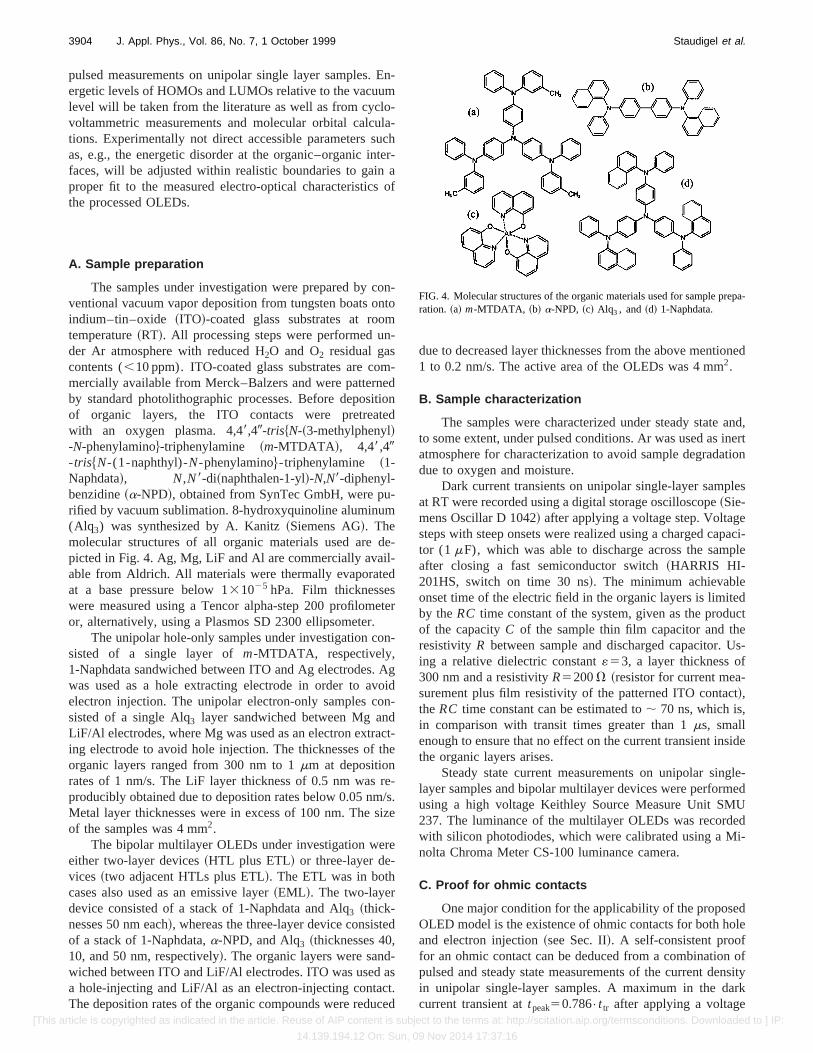
The samples under investigation were prepared by con-ventional vacuum vapor deposition from tungsten boats ontoindium–tin–oxide ~ITO!-coated glass substrates at roomtemperature~RT!. All processing steps were performed un-der Ar atmosphere with reduced H2O and O2 residual gascontents (,10 ppm). ITO-coated glass substrates are com-mercially available from Merck–Balzers and were patternedby standard photolithographic processes. Before depositionof organic layers, the ITO contacts were pretreatedwith an oxygen plasma. 4,48,49-tris$N-~3-methylphenyl!-N-phenylamino%-triphenylamine ~m-MTDATA !, 4,48,49-tris$N-(1-naphthyl)-N-phenylamino%-triphenylamine ~1-Naphdata!, N,N8-di~naphthalen-1-yl!-N,N8-diphenyl-benzidine~a-NPD!, obtained from SynTec GmbH, were pu-rified by vacuum sublimation. 8-hydroxyquinoline aluminum(Alq3) was synthesized by A. Kanitz~Siemens AG!. Themolecular structures of all organic materials used are de-picted in Fig. 4. Ag, Mg, LiF and Al are commercially avail-able from Aldrich. All materials were thermally evaporatedat a base pressure below 131025 hPa. Film thicknesseswere measured using a Tencor alpha-step 200 profilometeror, alternatively, using a Plasmos SD 2300 ellipsometer.
The unipolar hole-only samples under investigation con-sisted of a single layer ofm-MTDATA, respectively,1-Naphdata sandwiched between ITO and Ag electrodes. Agwas used as a hole extracting electrode in order to avoidelectron injection. The unipolar electron-only samples con-sisted of a single Alq3 layer sandwiched between Mg andLiF/Al electrodes, where Mg was used as an electron extract-ing electrode to avoid hole injection. The thicknesses of theorganic layers ranged from 300 nm to 1mm at depositionrates of 1 nm/s. The LiF layer thickness of 0.5 nm was re-producibly obtained due to deposition rates below 0.05 nm/s.Metal layer thicknesses were in excess of 100 nm. The sizeof the samples was 4 mm2.
The bipolar multilayer OLEDs under investigation wereeither two-layer devices~HTL plus ETL! or three-layer de-vices ~two adjacent HTLs plus ETL!. The ETL was in bothcases also used as an emissive layer~EML!. The two-layerdevice consisted of a stack of 1-Naphdata and Alq3 ~thick-nesses 50 nm each!, whereas the three-layer device consistedof a stack of 1-Naphdata,a-NPD, and Alq3 ~thicknesses 40,10, and 50 nm, respectively!. The organic layers were sand-wiched between ITO and LiF/Al electrodes. ITO was used asa hole-injecting and LiF/Al as an electron-injecting contact.The deposition rates of the organic compounds were reduced
due to decreased layer thicknesses from the above mentioned1 to 0.2 nm/s. The active area of the OLEDs was 4 mm2.
B. Sample characterization
The samples were characterized under steady state and,to some extent, under pulsed conditions. Ar was used as inertatmosphere for characterization to avoid sample degradationdue to oxygen and moisture.
Dark current transients on unipolar single-layer samplesat RT were recorded using a digital storage oscilloscope~Sie-mens Oscillar D 1042! after applying a voltage step. Voltagesteps with steep onsets were realized using a charged capaci-tor (1 mF), which was able to discharge across the sampleafter closing a fast semiconductor switch~HARRIS HI-201HS, switch on time 30 ns!. The minimum achievableonset time of the electric field in the organic layers is limitedby theRC time constant of the system, given as the productof the capacityC of the sample thin film capacitor and theresistivity R between sample and discharged capacitor. Us-ing a relative dielectric constant«53, a layer thickness of300 nm and a resistivityR5200V ~resistor for current mea-surement plus film resistivity of the patterned ITO contact!,theRC time constant can be estimated to; 70 ns, which is,in comparison with transit times greater than 1ms, smallenough to ensure that no effect on the current transient insidethe organic layers arises.
Steady state current measurements on unipolar single-layer samples and bipolar multilayer devices were performedusing a high voltage Keithley Source Measure Unit SMU237. The luminance of the multilayer OLEDs was recordedwith silicon photodiodes, which were calibrated using a Mi-nolta Chroma Meter CS-100 luminance camera.
C. Proof for ohmic contacts
One major condition for the applicability of the proposedOLED model is the existence of ohmic contacts for both holeand electron injection~see Sec. II!. A self-consistent prooffor an ohmic contact can be deduced from a combination ofpulsed and steady state measurements of the current densityin unipolar single-layer samples. A maximum in the darkcurrent transient attpeak50.786•t tr after applying a voltage
FIG. 4. Molecular structures of the organic materials used for sample prepa-ration. ~a! m-MTDATA, ~b! a-NPD, ~c! Alq3 , and~d! 1-Naphdata.
3904 J. Appl. Phys., Vol. 86, No. 7, 1 October 1999 Staudigel et al.
[This article is copyrighted as indicated in the article. Reuse of AIP content is subject to the terms at: http://scitation.aip.org/termsconditions. Downloaded to ] IP:
14.139.194.12 On: Sun, 09 Nov 2014 17:37:16
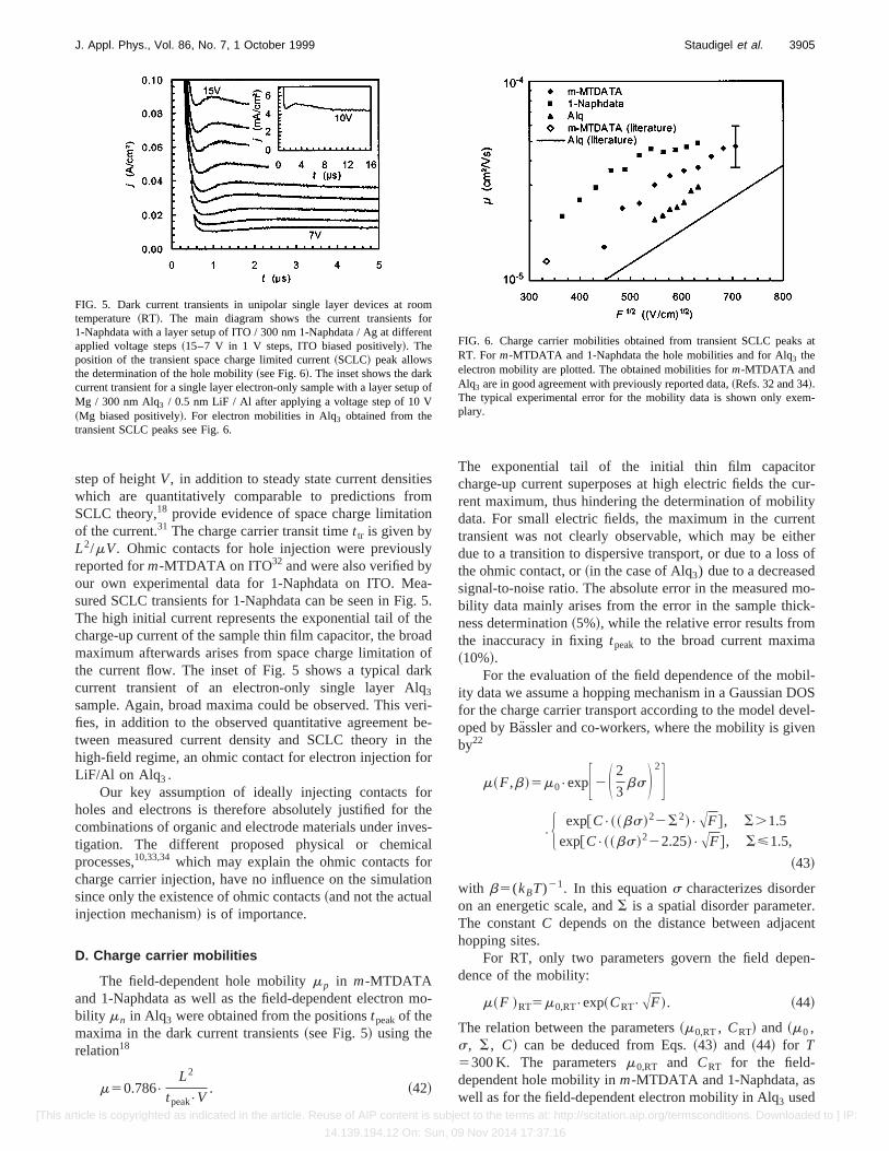
step of heightV, in addition to steady state current densitieswhich are quantitatively comparable to predictions fromSCLC theory,18 provide evidence of space charge limitationof the current.31 The charge carrier transit timet tr is given byL2/mV. Ohmic contacts for hole injection were previouslyreported form-MTDATA on ITO32 and were also verified byour own experimental data for 1-Naphdata on ITO. Mea-sured SCLC transients for 1-Naphdata can be seen in Fig. 5.The high initial current represents the exponential tail of thecharge-up current of the sample thin film capacitor, the broadmaximum afterwards arises from space charge limitation ofthe current flow. The inset of Fig. 5 shows a typical darkcurrent transient of an electron-only single layer Alq3
sample. Again, broad maxima could be observed. This veri-fies, in addition to the observed quantitative agreement be-tween measured current density and SCLC theory in thehigh-field regime, an ohmic contact for electron injection forLiF/Al on Alq3 .
Our key assumption of ideally injecting contacts forholes and electrons is therefore absolutely justified for thecombinations of organic and electrode materials under inves-tigation. The different proposed physical or chemicalprocesses,10,33,34 which may explain the ohmic contacts forcharge carrier injection, have no influence on the simulationsince only the existence of ohmic contacts~and not the actualinjection mechanism! is of importance.
D. Charge carrier mobilities
The field-dependent hole mobilitymp in m-MTDATAand 1-Naphdata as well as the field-dependent electron mo-bility mn in Alq3 were obtained from the positionstpeakof themaxima in the dark current transients~see Fig. 5! using therelation18
m50.786•L2
tpeak•V. ~42!
The exponential tail of the initial thin film capacitorcharge-up current superposes at high electric fields the cur-rent maximum, thus hindering the determination of mobilitydata. For small electric fields, the maximum in the currenttransient was not clearly observable, which may be eitherdue to a transition to dispersive transport, or due to a loss ofthe ohmic contact, or~in the case of Alq3) due to a decreasedsignal-to-noise ratio. The absolute error in the measured mo-bility data mainly arises from the error in the sample thick-ness determination~5%!, while the relative error results fromthe inaccuracy in fixingtpeak to the broad current maxima~10%!.
For the evaluation of the field dependence of the mobil-ity data we assume a hopping mechanism in a Gaussian DOSfor the charge carrier transport according to the model devel-oped by Ba¨ssler and co-workers, where the mobility is givenby22
m~F,b!5m0•expF2S 2
3bs D 2G
•H exp@C•~~bs!22S2!•AF#, S.1.5
exp@C•~~bs!222.25!•AF#, S<1.5,
~43!
with b5(kBT)21. In this equations characterizes disorderon an energetic scale, andS is a spatial disorder parameter.The constantC depends on the distance between adjacenthopping sites.
For RT, only two parameters govern the field depen-dence of the mobility:
m~F !RT5m0,RT•exp~CRT•AF !. ~44!
The relation between the parameters~m0,RT, CRT! and ~m0 ,s, S, C! can be deduced from Eqs.~43! and ~44! for T5300 K. The parametersm0,RT and CRT for the field-dependent hole mobility inm-MTDATA and 1-Naphdata, aswell as for the field-dependent electron mobility in Alq3 used
FIG. 5. Dark current transients in unipolar single layer devices at roomtemperature~RT!. The main diagram shows the current transients for1-Naphdata with a layer setup of ITO / 300 nm 1-Naphdata / Ag at differentapplied voltage steps~15–7 V in 1 V steps, ITO biased positively!. Theposition of the transient space charge limited current~SCLC! peak allowsthe determination of the hole mobility~see Fig. 6!. The inset shows the darkcurrent transient for a single layer electron-only sample with a layer setup ofMg / 300 nm Alq3 / 0.5 nm LiF / Al after applying a voltage step of 10 V~Mg biased positively!. For electron mobilities in Alq3 obtained from thetransient SCLC peaks see Fig. 6.
FIG. 6. Charge carrier mobilities obtained from transient SCLC peaks atRT. Form-MTDATA and 1-Naphdata the hole mobilities and for Alq3 theelectron mobility are plotted. The obtained mobilities form-MTDATA andAlq3 are in good agreement with previously reported data,~Refs. 32 and 34!.The typical experimental error for the mobility data is shown only exem-plary.
3905J. Appl. Phys., Vol. 86, No. 7, 1 October 1999 Staudigel et al.
[This article is copyrighted as indicated in the article. Reuse of AIP content is subject to the terms at: http://scitation.aip.org/termsconditions. Downloaded to ] IP:
14.139.194.12 On: Sun, 09 Nov 2014 17:37:16
for simulation, were therefore taken from straight line fitcurves to the measured data in lnm vs F1/2 plots ~see Fig. 6and Table I!. The measured hole mobilities inm-MTDATAand electron mobilities in Alq3 are in good agreement withpreviously reported data.32,24
The field-dependent hole mobility ina-NPD couldnot be obtained from dark current transients, since nomaxima in the transients were observed. Expecting no sig-nificant deviation from the hole mobility inN,N8-bis(3-methylphenyl)-N,N8-diphenylbenzidine~TPD!~the hole mobilities inm-MTDATA and 1-Naphdata are alsocomparable, see Fig. 6!, previously reported field-dependenthole mobilities for TPD were used for simulation~see TableI!.23 Furthermore, the hole mobility ofa-NPD is not ex-pected to be a critical parameter, since the thickness of thea-NPD layer in the devices under investigation is substan-tially smaller than the thicknesses of the adjacent 1-Naphdataand Alq3 layers.
For the electron mobilities inm-MTDATA, 1-Naphdata,anda-NPD ~respectively, the hole mobility in Alq3! we as-sumed 1% of the hole mobilities~respectively, the electronmobility!, which is a typical value in organic materials.35
E. Single-layer hole-only sample
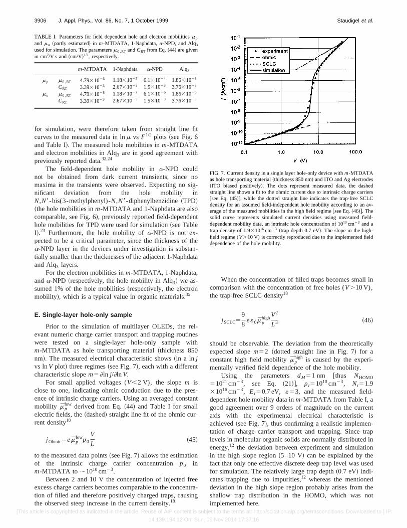
Prior to the simulation of multilayer OLEDs, the rel-evant numeric charge carrier transport and trapping routineswere tested on a single-layer hole-only sample withm-MTDATA as hole transporting material~thickness 850nm!. The measured electrical characteristic shows~in a ln jvs lnV plot! three regimes~see Fig. 7!, each with a differentcharacteristic slopem5] ln j/]ln V.
For small applied voltages (V,2 V), the slopem isclose to one, indicating ohmic conduction due to the pres-ence of intrinsic charge carriers. Using an averaged constantmobility mp
low derived from Eq.~44! and Table I for smallelectric fields, the~dashed! straight line fit of the ohmic cur-rent density18
j Ohmic5emplowp0
V
L~45!
to the measured data points~see Fig. 7! allows the estimationof the intrinsic charge carrier concentrationp0 inm-MTDATA to ;1010cm23.
Between 2 and 10 V the concentration of injected freeexcess charge carriers becomes comparable to the concentra-tion of filled and therefore positively charged traps, causingthe observed steep increase in the current density.18
When the concentration of filled traps becomes small incomparison with the concentration of free holes (V.10 V),the trap-free SCLC density18
j SCLC59
8««0mp
highV2
L3 ~46!
should be observable. The deviation from the theoreticallyexpected slopem52 ~dotted straight line in Fig. 7! for aconstant high field mobilitymp
high is caused by the experi-mentally verified field dependence of the hole mobility.
Using the parameters dM51 nm @thus NHOMO
51021cm23, see Eq. ~21!#, pi51010cm23, Nt51.931016cm23, Et50.7 eV, «53, and the measured field-dependent hole mobility data inm-MTDATA from Table I, agood agreement over 9 orders of magnitude on the currentaxis with the experimental electrical characteristic isachieved~see Fig. 7!, thus confirming a realistic implemen-tation of charge carrier transport and trapping. Since traplevels in molecular organic solids are normally distributed inenergy,12 the deviation between experiment and simulationin the high slope region~5–10 V! can be explained by thefact that only one effective discrete deep trap level was usedfor simulation. The relatively large trap depth~0.7 eV! indi-cates trapping due to impurities,12 whereas the mentioneddeviation in the high slope region probably arises from theshallow trap distribution in the HOMO, which was notimplemented here.
FIG. 7. Current density in a single layer hole-only device withm-MTDATAas hole transporting material~thickness 850 nm! and ITO and Ag electrodes~ITO biased positively!. The dots represent measured data, the dashedstraight line shows a fit to the ohmic current due to intrinsic charge carriers@see Eq.~45!#, while the dotted straight line indicates the trap-free SCLCdensity for an assumed field-independent hole mobility according to an av-erage of the measured mobilities in the high field regime@see Eq.~46!#. Thesolid curve represents simulated current densities using measured field-dependent mobility data, an intrinsic hole concentration of 1010 cm23 and atrap density of 1.931016 cm23 ~trap depth 0.7 eV!. The slope in the high-field regime (V.10 V) is correctly reproduced due to the implemented fielddependence of the hole mobility.
TABLE I. Parameters for field dependent hole and electron mobilitiesmp
and mn ~partly estimated! in m-MTDATA, 1-Naphdata,a-NPD, and Alq3used for simulation. The parametersm0 ,RT andCRT from Eq.~44! are givenin cm2/V s and~cm/V!1/2, respectively.
m-MTDATA 1-Naphdata a-NPD Alq3
mp m0 ,RT 4.7931026 1.1831025 6.131024 1.8631028
CRT 3.3931023 2.6731023 1.531023 3.7631023
mn m0 ,RT 4.7931028 1.1831027 6.131026 1.8631026
CRT 3.3931023 2.6731023 1.531023 3.7631023
3906 J. Appl. Phys., Vol. 86, No. 7, 1 October 1999 Staudigel et al.
[This article is copyrighted as indicated in the article. Reuse of AIP content is subject to the terms at: http://scitation.aip.org/termsconditions. Downloaded to ] IP:
14.139.194.12 On: Sun, 09 Nov 2014 17:37:16
F. Multilayer devices
The knowledge of the HOMO and LUMO levels of or-ganic materials used in OLEDs is of major importance for aproper understanding of the device behavior. The heights ofthe energetic barriers for charge carrier interface crossingused in the model, which are parameters with a high impacton simulation results, will be derived from these levels.
Cyclovoltammetric measurements for the first oxidationpotential of 1-Naphdata anda-NPD showed no significantdeviations to measurements performed onm-MTDATA andTPD, so that for the energetic levels of the HOMOs of1-Naphdata anda-NPD, reported data onm-MTDATA andTPD can be used.19 The deviations of the energetic levels ofthe LUMOs of 1-Naphdata anda-NPD relative to theLUMOs of m-MTDATA and TPD19 were calculated usingMOPAC ~none for a-NPD and approx. 0.4 eV lower for1-Naphdata!. The energetic positions of the HOMO andLUMO of Alq3 were taken from literature.19
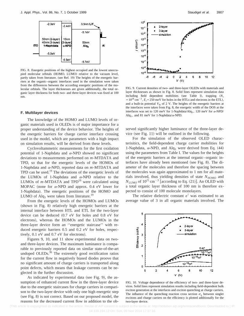
From the energetic levels of the HOMOs and LUMOs~shown in Fig. 8! relatively high energetic barriers at theinternal interface between HTL and ETL for the two-layerdevice can be deduced~0.7 eV for holes and 0.8 eV forelectrons!, whereas the HOMOs and the LUMOs in thethree-layer device form an ‘‘energetic staircase’’ with re-duced energetic barriers 0.5 and 0.2 eV for holes, respec-tively, 0.1 eV and 0.7 eV for electrons!.
Figures 9, 10, and 11 show experimental data on two-and three-layer devices. The maximum luminance is compa-rable to previously reported data on similar state-of-the-artundoped OLEDs.36 The extremely good rectification ratiosfor the current flow in negatively biased diodes proove thatno significant amount of charge carriers is transported alongpoint defects, which means that leakage currents can be ne-glected in the further discussion.
As indicated by experimental data~see Fig. 9!, the as-sumption of enhanced current flow in the three-layer devicedue to the energetic staircases for charge carriers in compari-son to the two-layer device with only one high energetic step~see Fig. 8! is not correct. Based on our proposed model, thereasons for the decreased current flow in addition to the ob-
served significantly higher luminance of the three-layer de-vice ~see Fig. 11! will be outlined in the following.
For the simulation of the observed OLED charac-terisitics, the field-dependent charge carrier mobilities for1-Naphdata,a-NPD, and Alq3 were derived from Eq.~44!using the parameters from Table I. The values for the heightsof the energetic barriers at the internal organic–organic in-terfaces have already been mentioned~see Fig. 8!. The di-ameter of the molecules and therefore the spacing betweenthe molecules was again approximated to 1 nm for all mate-rials involved, thus yielding densities of stateNHOMO andNLUMO of 1021cm23 @according to Eq.~21!#. An OLED witha total organic layer thickness of 100 nm is therefore ex-pected to consist of 100 molecule monolayers.
The relative dielectric constant« i was estimated to anaverage value of 3 in all organic materials involved. The
FIG. 8. Energetic positions of the highest occupied and the lowest unoccu-pied molecular orbitals~HOMO, LUMO! relative to the vacuum level,partly taken from literature.~see Ref. 19! The heights of the energetic bar-riers at the organic–organic interfaces used in the simulation were takenfrom the differences between the according energetic positions of the mo-lecular orbitals. The layer thicknesses are given additionally, the total or-ganic layer thickness for both two- and three-layer devices was fixed at 100nm.
FIG. 9. Current densities of two- and three-layer OLEDs with materials andlayer thicknesses as shown in Fig. 8. Solid lines represent simulation dataincluding field dependent mobilities~see Table I!, trapping ~Nt
51018 cm23, Et5250 meV for holes in the HTLs and electrons in the ETL!,and a built-in potentialVbi of 2 V. The heights of the energetic barriers atthe interfaces were taken from Fig. 8, the energetic width of the DOS at theinterfaces was set to 120 meV for 1-Naphdata/Alq3 , 120 meV fora-NPD/Alq3 , and 81 meV for 1-Naphdata/a-NPD.
FIG. 10. Voltage dependence of the efficiency of two- and three-layer de-vices. Solid lines represent simulation results including field-dependent bulkexciton generation at the interfaces and exciton quenching at charge carriers.The influence of the quenching reaction cross sectionsq between singletexcitons and charge carriers on the efficiency is plotted additionally for thetwo-layer device.
3907J. Appl. Phys., Vol. 86, No. 7, 1 October 1999 Staudigel et al.
[This article is copyrighted as indicated in the article. Reuse of AIP content is subject to the terms at: http://scitation.aip.org/termsconditions. Downloaded to ] IP:
14.139.194.12 On: Sun, 09 Nov 2014 17:37:16
total outcoupling efficiency of the internally emitted photons,considering waveguiding losses (hwave) and absorption(habs), was estimated to 30%. The fraction of radiative de-cayhbulk of Alq3 singlet excitons, which is equivalent to thefluorescence quantum yield, was also set to 30% in accor-dance with previously reported data.37 The lifetime ts ofsinglet excitons was set to a typical value for organic mate-rials ~10 ns!,21 and the average numberNhop of hopping pro-cesses during the lifetime was set to 10, which is compatibleto reported literature data.38 The widthLq of the quenchingzone at the electrodes@see Eq.~34!#, a parameter of minorimportance, was estimated to be 2 nm.
As unknown parameters remain the built-in potentialVbi , trap densitiesNt,p
i andNt,ni , trap depthsEt,p
i andEt,ni ,
as well as the energetic disorders at the interfacess and thereaction cross sectionsq for singlet exciton quenching atcharge carriers.
The dotted curve in Fig. 9 represents the simulation ofthe trap-free current density in a two-layer device, which hasshown to be practically independent of the energetic disorderat the internal interface between HTL and ETL. The built-inpotential, trap densities and trap depths were then adjusted tofit the simulation results to the experimental data. The mea-sured current density for a two-layer device can be repro-duced over 4 orders of magnitude using a built-in potentialof 2 V, trap densities for holes in 1-Naphdata and for elec-trons in Alq3 of 1018cm23 with trap depths of 250 meV.This large amount of discrete shallow traps, which decreasesthe current density but does not alter the shape of the simu-lation curve~as it would be the case, e.g., for an exponentialtrap distribution11,18!, can be justified with structural defectsin the disordered amorphous films rather than with impuri-ties, which would lead to deeper traps with smaller trapdensities.12 The value of 250 meV is comparable to reportedtrap depths derived from thermally stimulated luminescencemeasurements.39 For holes in the ETL and electrons in theHTLs no trapping was considered, since the mobilities arealready assumed to be two orders of magnitude smaller.
In contrast to the current density, the device efficiencydepends strongly on the energetic disorders at the internal
interface. That is clear evidence for the fact that the majorityof charge carriers recombines at the interface between HTLand ETL, where the probability for the formation of a bulkexciton from an interface exciton depends strongly on theinterface barrier crossing probabilities of the charge carriers.The two-layer device efficiency can be quantitatively repro-duced by adjusting the energetic disorders to 120 meV andthe quenching cross sectionsq to 10216m2 ~see Fig. 10, theinfluence ofsq on the efficiency is shown additionally!. Theobtained value for the quenching cross sectionsq is surpris-ingly high ~cross-section diameter equals several timesdM),which may be due to the fact that exciton dissociation in theelectric field is not considered, as already mentioned.
The increase of the device efficiency for operation volt-agesV exceeding the onset voltage~equivalent toVbi! arisesmainly from the electric field dependence of the bulk excitonformation probability at the interfaces@see Eqs.~25!, ~27!,and ~28!#. The efficiency decrease at higher voltages resultsfrom exciton quenching at free and trapped charge carriers.The ratio between the emission and this quenching mecha-nism decreases with increasing electric field due to the in-crease of the total number of charge carriers in the device@see Eqs.~35! and ~36!#.
Naturally, with the correct simulation of device currentdensity and efficiency~which is a major result of our paper!,the luminance of the two-layer device is also reproducedover 4 orders of magnitude~see Fig. 11!.
The additional third organic layer~10 nm a-NPD! be-tween the HTL and ETL is not expected to change any of theabove mentioned parameters. The charge carrier trapping inthe new second HTL layer is assumed to be same as in thefirst HTL. Therefore the energetic disorders at the twoorganic–organic interfaces remain as the only possible freeparameters to fit the simulation results to experimental data.The energetic disorder at thea-NPD/Alq3 interface was setto the same value used for the 1-Naphdata/Alq3 interface~120 meV!, whereas the energetic disorder at the1-Naphdata/a-NPD interface was adjusted to 81 meV.
Using these energetic disorders, the decreased currentdensity, the higher device efficiency, and the increased lumi-nance of the three-layer device can be reproduced, with avery good agreement between simulation and experimentaldata for applied voltages exceeding 4 V~see Figs. 9–11!.
IV. DISCUSSION
The model is able to quantitatively reproduce the char-acteristics of hole-only single-layer samples and of bipolartwo- and three-layer OLEDs, as the comparison with experi-ment has shown~see Figs. 7, 9, 10, and 11!. The experimen-tally not direct accessible parameters, adjusted to fit the re-sults to experimental data, remained within realisticboundaries.
Extensive parameter studies have verified that only onesolution exists which simultaneously describes the behaviorof both two- and three-layer devices correctly. This solutionis defined~in dependence of the applied voltage! by the spa-tial distribution of the values of the variables of state, namelycharge carrier densities and singlet exciton density, which
FIG. 11. Luminance of two- and three-layer OLEDs corresponding to Figs.9 and 10. The model predictions are quantitatively in good agreement withexperimental data, particularly in the technologically relevant range for pas-sive matrix displays from 1000 to 10 000 cd/m2.
3908 J. Appl. Phys., Vol. 86, No. 7, 1 October 1999 Staudigel et al.
[This article is copyrighted as indicated in the article. Reuse of AIP content is subject to the terms at: http://scitation.aip.org/termsconditions. Downloaded to ] IP:
14.139.194.12 On: Sun, 09 Nov 2014 17:37:16
allow a physical interpretation of the different device behav-iors.
Nevertheless, it should be clear that the choice of un-known parameters for reproducing the electro-optical char-acteristics of the processed two- and three-layer OLEDs isnot a singular one, since the actual solution is influencedonly by combinations of parameters. For example, the num-ber of trapped charge carriers and, therefore, also the currentdensity depends simultaneously on the parameters trapdepth, trap concentration, and density of states in the HOMO~respectively, LUMO!. Changes in one parameter~e.g., trapdepth! can often~to a certain extent! be compensated byadjusting other parameters~e.g., trap concentration!. Thesame applies for the energetic disorder parameters at inter-nal interfaces, which is strongly coupled to the energeticheight of the barriers for charge carrier interface crossing~which has a high experimental error of about 0.1 eV!, sinceonly the interface barrier crossing probabilityG, a functionof both parameters, is of importance for the simulation.
The different electro-optical characteristics of the two-and three-layer devices presented in this paper arise mainlyfrom the different spatial distribution of the charge carrieraccumulations. In two-layer OLEDs, the holes are stored infront of the HTL/ETL interface in direct contact with theelectrons accumulated behind this interface~see Fig. 12!.Therefore interface recombination plays a major role in thetotal recombination. The low device efficiency can be ex-plained with the inefficient generation of bulk excitons at the
interface, since the energetic barriers for charge carrier inter-face crossing are relatively high~see Fig. 8!.
In contrast, in the three-layer device the holes are accu-mulated before the interface between the two HTLs~sincethere it is the highest barrier!, whereas the electrons arestored after the interface between the second HTL and theETL ~see Fig. 13!. These two charge carrier reservoirs areseparated by the thina-NPD layer, thus reducing the directinterface recombination and, due to the builtup of large spacecharges reducing the electric field and the charge carrier ve-locity in the first HTL and in the ETL~see Fig. 13!, also thecurrent density~see Fig. 9!.
The high energetic barrier for electrons at the HTL/ETLinterface causes an accumulation of electrons in the ETLbulk near this interface, with only very few electrons enter-ing the adjacent HTL. For charge carrier recombination, theholes have to cross the 1-Naphdata/a-NPD interface by nor-mal hopping processes~drift and diffusion! to arrive at thea-NPD/Alq3 interface. Since the energetic barrier for holesat this HTL/ETL interface is significantly reduced for thethree-layer device in comparison with the two-layer device,interface recombination becomes a very effective source forbulk excitons, thus yielding a higher device luminance inspite of the decreased current density. Additionally, the holescan easily enter the ETL bulk for further direct bulk excitonformation.
FIG. 12. Spatial distribution of the electric field, the energetic postions ofthe HOMO and the LUMO, the free and trapped charge carrier densities,and the singlet exciton density along thez axis in a two-layer device for anapplied voltage of 8 V. The HTL/ETL interface is marked by the verticalsolid line. The dashed line represents the average electric field.
FIG. 13. Spatial distribution of the electric field, the energetic postions ofthe HOMO and the LUMO, the free and trapped charge carrier densities,and the singlet exciton density along thez axis in a three-layer device for anapplied voltage of 8 V. The organic–organic interfaces are again marked byvertical solid lines. The dashed line again represents the average electricfield.
3909J. Appl. Phys., Vol. 86, No. 7, 1 October 1999 Staudigel et al.
[This article is copyrighted as indicated in the article. Reuse of AIP content is subject to the terms at: http://scitation.aip.org/termsconditions. Downloaded to ] IP:
14.139.194.12 On: Sun, 09 Nov 2014 17:37:16
Summarizing both the experimental and simulation workof this paper, two main aspects have to be outlined. First, wehave shown the relevance of our model for the study of state-of-the-art vapor-deposited OLEDs by experimentally verify-ing the key assumption of two ohmic contacts and by a quan-titative reproduction of electro-optical device characterstics.Second, from the insight into the spatial distribution of thecharge carrier accumulation zones, we have explained theenhanced luminance and device efficiency of three-layer de-vices relative to two-layer devices.
V. CONCLUDING REMARKS
The proposed model can also be applied to a large vari-ety of other materials and different multilayer OLED archi-tectures, even for the case of injection limitation for onecharge carrier species. Additionally, time-dependent phe-nomena like luminance onset and offset can be simulated,and even impedance spectra are possible in the case wherecomputer power is no limitation. The model can easily bemodified to include spatial variations in trap densities, dop-ing of emissive layers, or extra charge carrier blocking lay-ers.
We expect from the quantitative simulation of ourOLEDs a positive impact on further device optimization,such as improved efficiency and operating voltage. For ex-ample, instead of performing time-consuming experimentsfor layer thickness optimization in multilayer OLEDS, a hintfor the ideal layer setup can be derived from calculations.This method can also be used to align the operating voltagesof different colored pixels in multicolor flat panel displaysbased on OLED technology.
Naturally, the simulation results depend strongly on theparameter values used, so that the determination of unknownparameters remains a crucial point to further ensure thephysical relevance. The severest limitation for large param-eter studies, in order to gain some insight into the qualitativebehavior of OLEDs, is given by the long calculation times,which are on the order of days on common Pentium II PCsfor a complete electro-optical characteristic.
In conclusion, we have shown in comparison with ex-perimental data the applicability of our model for quantita-tive simulations of multilayer OLED properties. We haveoutlined the different mechanisms governing the behavior oftwo- and three-layer devices and the implications on deviceperformance.
ACKNOWLEDGMENTS
The authors would like to thank J. Gudarslu, G. Witt-mann, and J. Schumann for technical help, A. Kanitz forsynthesizing the Alq3 and performing molecular orbital cal-culations, A. Richter from SynTec GmbH for providing thecyclovoltammetric measurement data, and H. v. Seggern andR. Helbig for helpful discussions. Support from theBundesministerium fu¨r Bildung und Forschung~Grant No.BMBF-Project 01 BK 703/4! is gratefully acknowledged.
1C. W. Tang and S. A. VanSlyke, Appl. Phys. Lett.51, 913 ~1987!.2C. W. Tang, S. A. VanSlyke, and C. H. Chen, J. Appl. Phys.65, 3610~1989!.
3J. H. Burroughes, D. D. C. Bradley, A. R. Brown, R. N. Marks, K.MacKay, R. H. Friend, P. L. Burn, and A. B. Holmes, Nature~London!347, 539 ~1990!.
4D. Braun and A. J. Heeger, Appl. Phys. Lett.58, 1982~1991!.5I. D. Parker, J. Appl. Phys.75, 1656~1994!.6D. V. Khramtchenkov, H. Ba¨ssler, and V. I. Arkhipov, J. Appl. Phys.79,9283 ~1996!.
7D. V. Khramtchenkov, V. I. Arkhipov, and H. Ba¨ssler, J. Appl. Phys.81,6954 ~1997!.
8Y.-H. Tak and H. Ba¨ssler, J. Appl. Phys.81, 6963~1997!.9H. Bassler, Y. H. Tak, D. V. Khramtchenkov, and V. R. Nikitenko, Synth.Met. 91, 173 ~1997!.
10V. I. Arkhipov, E. V. Emelianova, Y. H. Tak, and H. Ba¨ssler, J. Appl.Phys.84, 848 ~1998!.
11P. E. Burrows, Z. Shen, V. Bulovic, D. M. McCarty, S. R. Forrest, J. A.Cronin, and M. E. Thompson, J. Appl. Phys.79, 7991~1996!.
12A. J. Campbell, D. D. C. Bradley, and D. G. Lidzey, J. Appl. Phys.82,6326 ~1997!.
13P. S. Davids, I. H. Campbell, and D. L. Smith, J. Appl. Phys.82, 6319~1997!.
14B. K. Crone, P. S. Davids, I. H. Campbell, and D. L. Smith, J. Appl. Phys.84, 833 ~1998!.
15J. Shen and J. Yang, J. Appl. Phys.83, 7706~1998!.16J. Yang and J. Shen, J. Appl. Phys.84, 2105~1998!.17J. C. Scott, S. A. Carter, S. Karg, and M. Angelopoulos, Proc. SPIE3002,
86 ~1997!.18M. A. Lampert and P. Mark,Current Injection in Solids~Academic, New
York, 1970!.19Z. Zhang, X. Jiang, S. Xu, T. Nagatomo, and O. Omoto, Synth. Met.91,
131 ~1997!.20G. Hammerlin and K.-H. Hoffmann,Numerische Mathematik~Springer,
Berlin, 1989!.21J. B. Birks, Photophysics of Aromatic Molecules~Wiley-Interscience,
London, 1970!.22H. Bassler, Phys. Status Solidi B175, 15 ~1993!.23M. Stolka, J. F. Yanus, and D. M. Pai, J. Phys. Chem.88, 4707~1984!.24B. Chen and S. Liu, Synth. Met.91, 169 ~1997!.25U. Albrecht and H. Ba¨ssler, Phys. Status Solidi B191, 455 ~1995!.26K. C. Kao and W. Hwang,Electrical Transport in Solids~Pergamon,
Oxford, 1981!.27W. Stampor, J. Kalinowski, P. Di Marco, and V. Fattori, Appl. Phys. Lett.
70, 1935~1997!.28N. C. Greenham, R. H. Friend, and D. C. Bradley, Adv. Mater.6, 491
~1994!.29L. Bergmann and C. Schaefer,Optik ~de Gruyter, Berlin, 1993!.30G. Gu, D. Z. Garbuzov, P. E. Burrows, S. R. Venkatesh, S. R. Forrest, and
M. E. Thompson, Opt. Lett.22, 396 ~1997!.31M. Abkowitz and D. M. Pai, Philos. Mag. B53, 193 ~1986!.32C. Giebeler, H. Antoniadis, D. D. C. Bradley, and Y. Shirota, Appl. Phys.
Lett. 72, 2448~1998!.33L. S. Hung, C. W. Tang, and M. G. Mason, Appl. Phys. Lett.70, 152
~1996!.34R. Schlaf, B. A. Parkinson, P. A. Lee, K. W. Nebesny, G. Jabbour, B.
Kippelen, N. Peyghambarian, and N. R. Armstrong, J. Appl. Phys.84,6729 ~1998!.
35D. Adam, PhD thesis, University of Bayreuth, 1994.36Y. Shirota, Y. Kuwabara, H. Inada, T. Wakimoto, H. Nakada, Y.
Yonemoto, S. Kawami, and K. Imai, Appl. Phys. Lett.65, 807 ~1994!.37D. Z. Garbuzov, S. R. Forrest, A. G. Tsekoun, P. E. Burrows, V. Bulovic,
and M. E. Thompson, J. Appl. Phys.80, 4644~1996!.38T. Mori, K. Obata, K. Miyachi, T. Mizutani, and Y. Kawakami, Jpn. J.
Appl. Phys., Part 136, 7239~1997!.39E. W. Forsythe, D. C. Morton, C. W. Tang, and Y. Gao, Appl. Phys. Lett.
73, 1457~1998!.
3910 J. Appl. Phys., Vol. 86, No. 7, 1 October 1999 Staudigel et al.
[This article is copyrighted as indicated in the article. Reuse of AIP content is subject to the terms at: http://scitation.aip.org/termsconditions. Downloaded to ] IP:
14.139.194.12 On: Sun, 09 Nov 2014 17:37:16