Embed Size (px)
Citation preview
AT & S Austria Technologie & Systemtechnik Aktiengesellschaft | Fabriksgasse13 | A-8700 Leoben Tel +43 (0) 3842 200-0 | E-Mail [email protected]
www.ats.net
AT&S first choice for advanced applications
Company Presentation
September 2015
1
Company Overview
Strategy & Market
Annex
Financials
Table of Contents
2
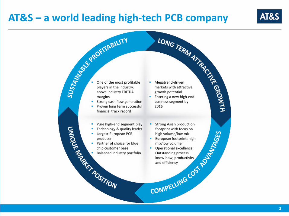
AT&S – a world leading high-tech PCB company
Megatrend-driven markets with attractive growth potential
Entering a new high-end business segment by 2016
Pure high-end segment play Technology & quality leader Largest European PCB
producer Partner of choice for blue
chip customer base Balanced industry portfolio
Strong Asian production footprint with focus on high volume/low mix
European footprint: high mix/low volume
Operational excellence: Outstanding process know-how, productivity and efficiency
One of the most profitable players in the industry: above industry EBITDA margins
Strong cash flow generation Proven long term successful
financial track record
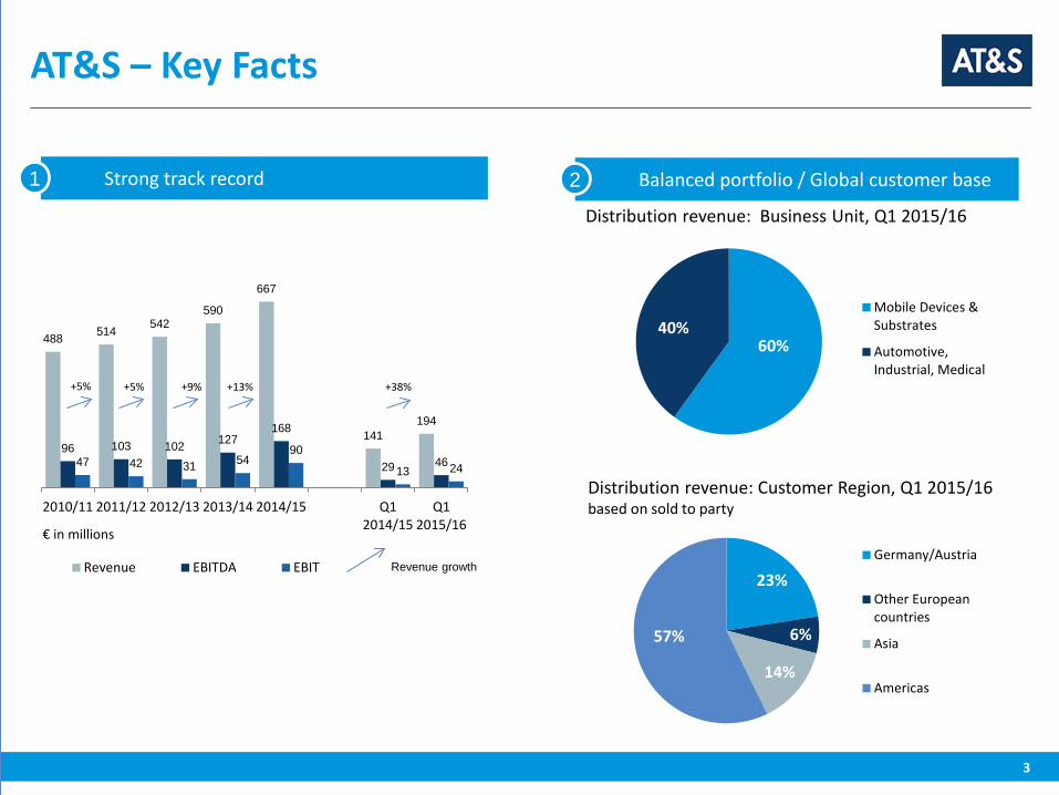
AT&S – Key Facts
Strong track record 1 Balanced portfolio / Global customer base 2
7%
€ in millions
3
Distribution revenue: Business Unit, Q1 2015/16
Distribution revenue: Customer Region, Q1 2015/16 based on sold to party
23%
6%
14%
57%
Germany/Austria
Other Europeancountries
Asia
Americas
60% 40%
Mobile Devices &Substrates
Automotive,Industrial, Medical
488 514 542 590
667
141 194
96 103 102 127 168
29 46 47 42 31 54 90
13 24
2010/11 2011/12 2012/13 2013/14 2014/15 Q12014/15
Q12015/16
Revenue EBITDA EBIT
+5% +5% +9% +13% +38%
Revenue growth
4
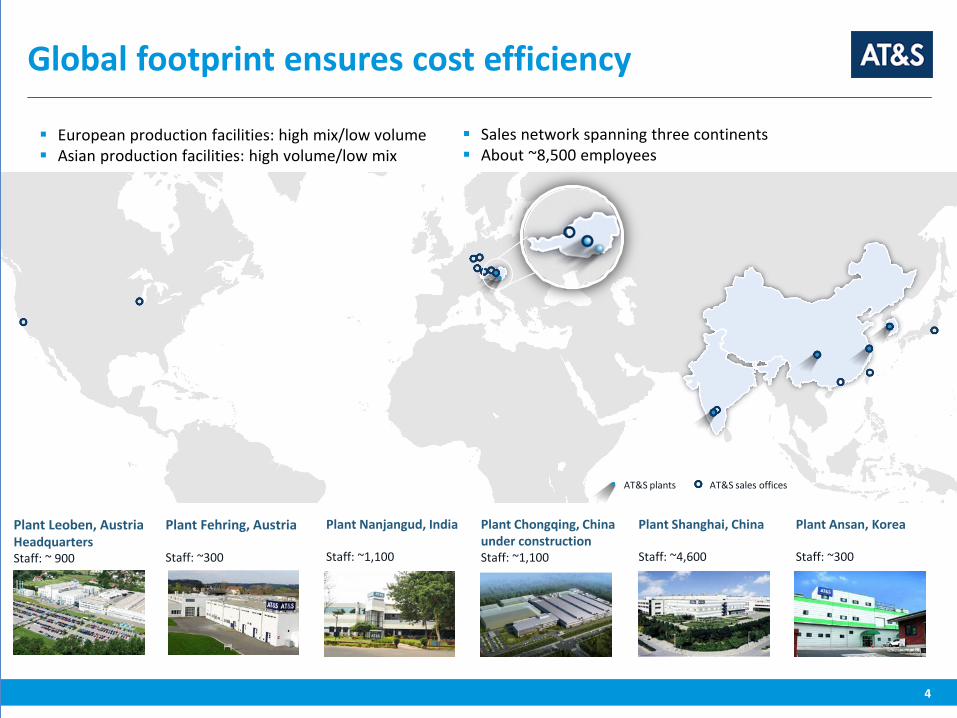
Global footprint ensures cost efficiency
European production facilities: high mix/low volume Asian production facilities: high volume/low mix
Sales network spanning three continents About ~8,500 employees
Plant Shanghai, China Staff: ~4,600
Plant Ansan, Korea Staff: ~300
Plant Nanjangud, India Staff: ~1,100
Plant Chongqing, China under construction Staff: ~1,100
Plant Leoben, Austria Headquarters Staff: ~ 900
Plant Fehring, Austria Staff: ~300
AT&S sales offices AT&S plants
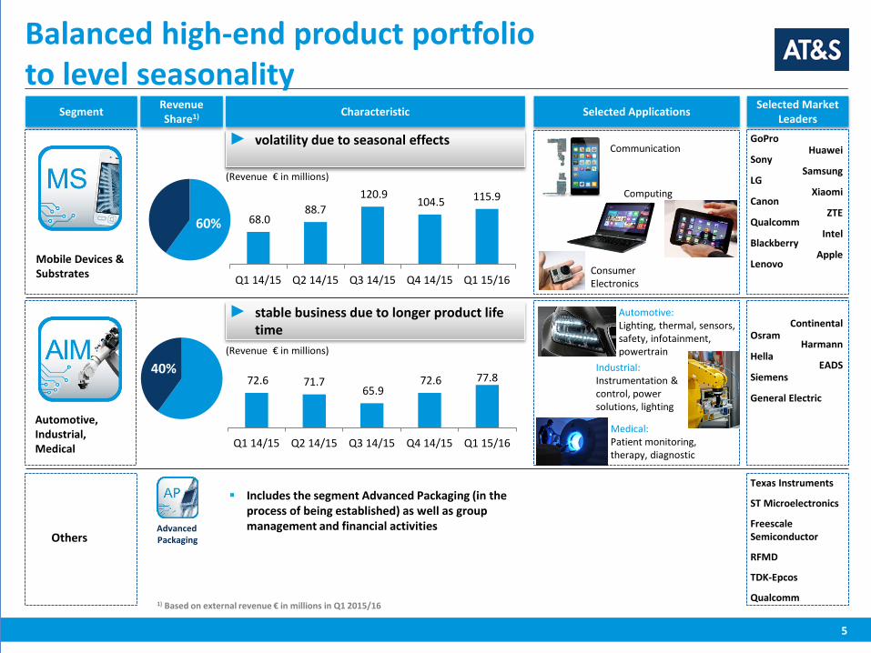
68.0 88.7
120.9 104.5 115.9
-
50,0
100,0
150,0
Q1 14/15 Q2 14/15 Q3 14/15 Q4 14/15 Q1 15/16
72.6 71.7 65.9
72.6 77.8
50,0 60,0 70,0 80,0
Q1 14/15 Q2 14/15 Q3 14/15 Q4 14/15 Q1 15/16
► volatility due to seasonal effects
5
Balanced high-end product portfolio to level seasonality
Characteristic
Selected Applications
Segment
1) Based on external revenue € in millions in Q1 2015/16
Mobile Devices & Substrates
Advanced Packaging
Selected Market Leaders
GoPro
Sony
LG
Canon
Qualcomm
Blackberry
Lenovo
Huawei
Samsung
Xiaomi
ZTE
Intel
Apple
► stable business due to longer product life time
Includes the segment Advanced Packaging (in the process of being established) as well as group management and financial activities
Others
(Revenue € in millions)
(Revenue € in millions)
Automotive, Industrial, Medical
Revenue Share1)
Communication
Computing
Automotive: Lighting, thermal, sensors, safety, infotainment, powertrain
Medical: Patient monitoring, therapy, diagnostic
Industrial: Instrumentation & control, power solutions, lighting
Consumer Electronics
Osram
Hella
Siemens
General Electric
Continental
Harmann
EADS
Texas Instruments
ST Microelectronics
Freescale Semiconductor
RFMD
TDK-Epcos
Qualcomm
60%
40%
6
Company Overview
Strategy & Market
Annex
Financials
Table of Contents
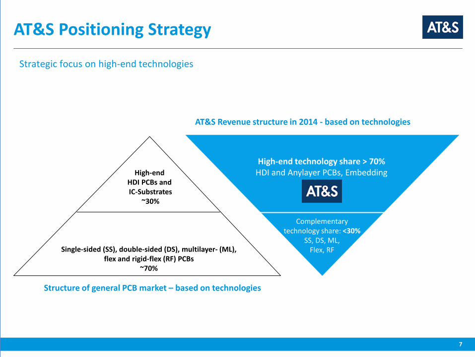
AT&S Positioning Strategy
Strategic focus on high-end technologies
High-end HDI PCBs and IC-Substrates
~30%
High-end technology share > 70% HDI and Anylayer PCBs, Embedding
Complementary technology share: <30%
SS, DS, ML, Flex, RF
Structure of general PCB market – based on technologies
Single-sided (SS), double-sided (DS), multilayer- (ML), flex and rigid-flex (RF) PCBs
~70%
AT&S Revenue structure in 2014 - based on technologies
7
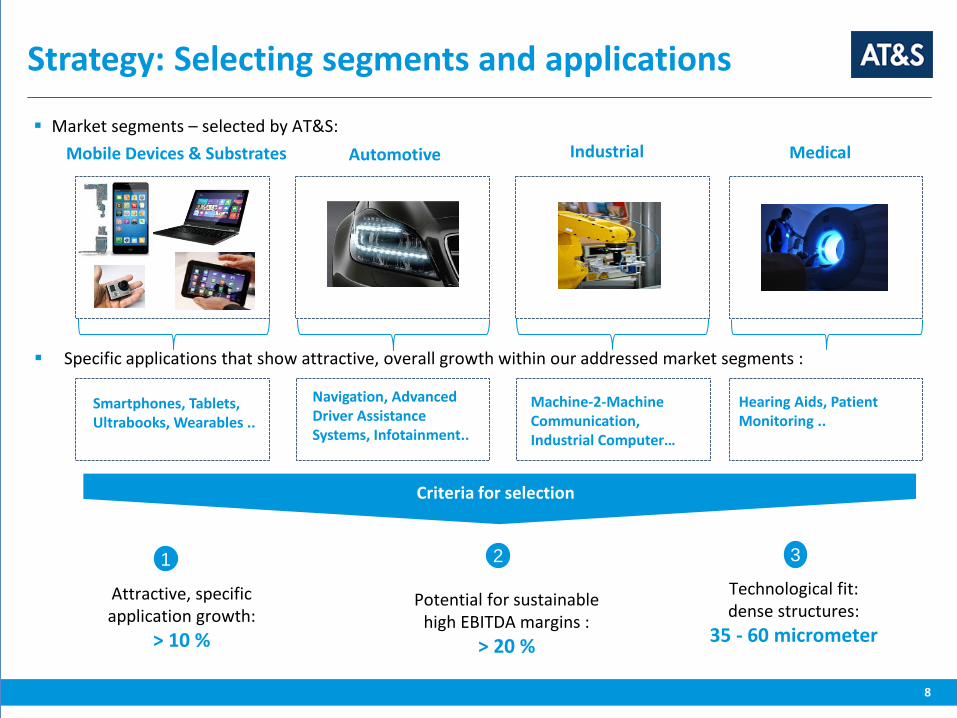
Strategy: Selecting segments and applications
Market segments – selected by AT&S:
Mobile Devices & Substrates Automotive Industrial Medical
Attractive, specific application growth:
> 10 %
Potential for sustainable high EBITDA margins :
> 20 %
Technological fit: dense structures:
35 - 60 micrometer
Criteria for selection
Smartphones, Tablets, Ultrabooks, Wearables ..
Navigation, Advanced Driver Assistance Systems, Infotainment..
Machine-2-Machine Communication, Industrial Computer…
Hearing Aids, Patient Monitoring ..
1 2 3
Specific applications that show attractive, overall growth within our addressed market segments :
8
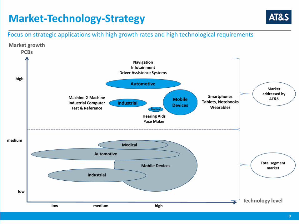
Market-Technology-Strategy Focus on strategic applications with high growth rates and high technological requirements Market growth
PCBs
Technology level
Total segment market
Market addressed by
AT&S
low
medium
high
Mobile Devices
Mobile Devices Industrial
Automotive
low
medium high
Medical
Industrial
Automotive
Medical
Smartphones Tablets, Notebooks
Wearables
Navigation Infotainment
Driver Assistence Systems
Machine-2-Machine Industrial Computer
Test & Reference
Hearing Aids Pace Maker
9
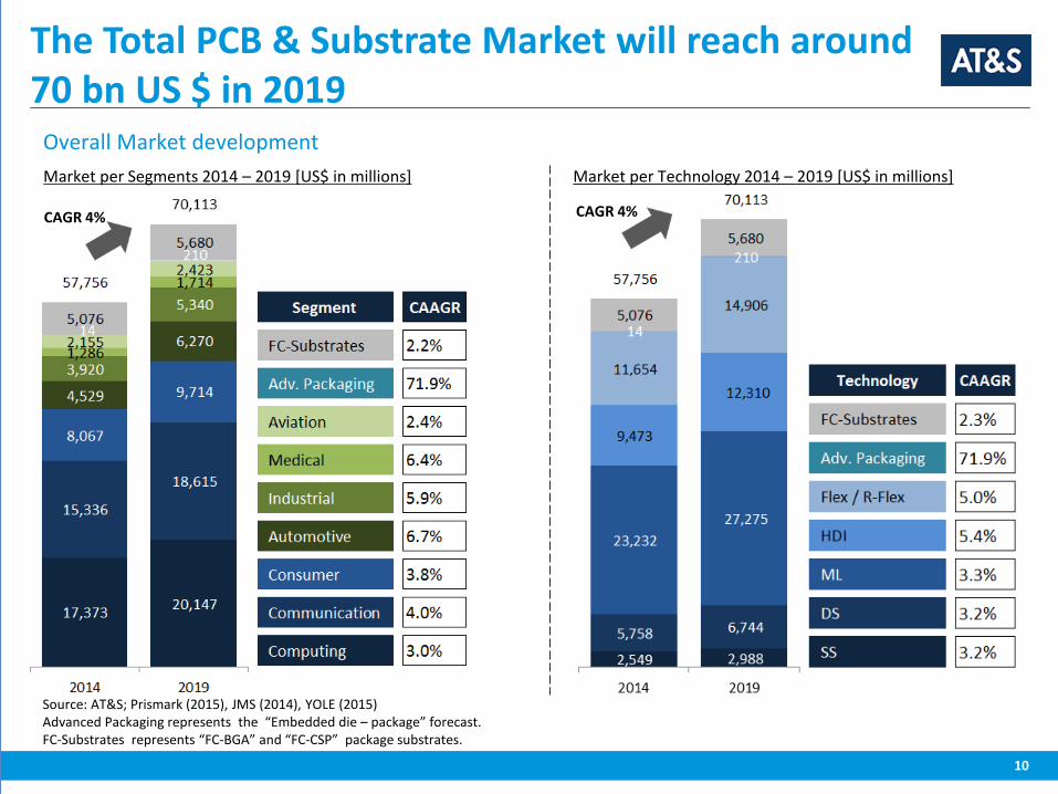
Source: AT&S; Prismark (2015), JMS (2014), YOLE (2015) Advanced Packaging represents the “Embedded die – package” forecast. FC-Substrates represents “FC-BGA” and “FC-CSP” package substrates.
Market per Segments 2014 – 2019 [US$ in millions]
The Total PCB & Substrate Market will reach around 70 bn US $ in 2019
Overall Market development Market per Technology 2014 – 2019 [US$ in millions]
10
CAGR 4% CAGR 4%
11
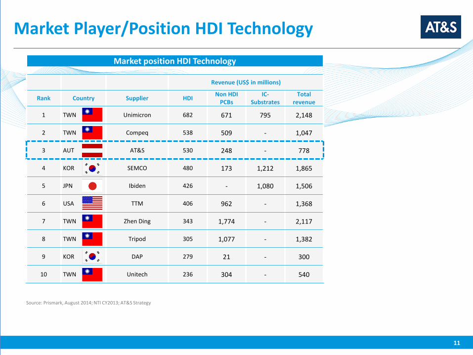
Market Player/Position HDI Technology
Source: Prismark, August 2014; NTI CY2013; AT&S Strategy
Market position HDI Technology
Revenue (US$ in millions)
Rank Country Supplier HDI Non HDI PCBs
IC-Substrates
Total revenue
1 TWN Unimicron 682 671 795 2,148
2 TWN Compeq 538 509 - 1,047
3 AUT AT&S 530 248 - 778
4 KOR SEMCO 480 173 1,212 1,865
5 JPN Ibiden 426 - 1,080 1,506
6 USA TTM 406 962 - 1,368
7 TWN Zhen Ding 343 1,774 - 2,117
8 TWN Tripod 305 1,077 - 1,382
9 KOR DAP 279 21 - 300
10 TWN Unitech 236 304 - 540
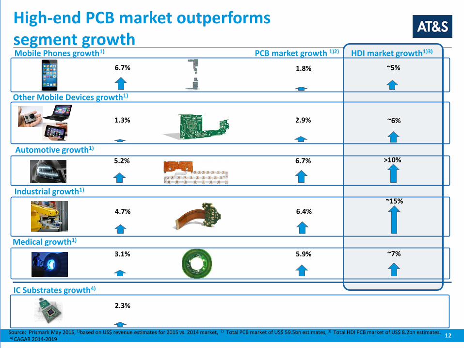
Automotive growth1)
High-end PCB market outperforms segment growth Mobile Phones growth1)
Industrial growth1)
Medical growth1)
12
Other Mobile Devices growth1)
PCB market growth 1)2) HDI market growth1)3)
Source: Prismark May 2015, 1)based on US$ revenue estimates for 2015 vs. 2014 market, 2) Total PCB market of US$ 59.5bn estimates, 3) Total HDI PCB market of US$ 8.2bn estimates. 4) CAGAR 2014-2019
5.2%
IC Substrates growth4)
4.7%
3.1%
2.3%
6.7%
6.4%
5.9%
>10%
~15%
~7%
6.7%
1.3%
1.8%
2.9% ~6%
~5%
13
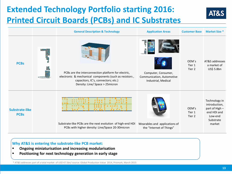
General Description & Technology Application Areas Customer Base Market Size *
PCBs
PCBs are the interconnection platform for electric, electronic & mechanical components (such as resistors ,
capacitors, IC’s, connectors; etc.) Density: Line/ Space > 25micron
Computer, Consumer, Communication, Automotive
Industrial, Medical
OEM´s Tier 1 Tier 2
AT&S addresses a market of US$ 5.8bn
Substrate-like PCBs
Substrate-like PCBs are the next evolution of high-end HDI PCBs with higher density: Line/Space 20-30micron
Wearables and applications of the “Internet of Things”
OEM’s Tier 1 Tier 2
Technology in introduction, part of High –end HDI and
Low-end Substrate
market
* AT&S addresses part of a total market of USD 47.5bn/ source: Global Production Value 2014, Prismark, March 2015
Extended Technology Portfolio starting 2016: Printed Circuit Boards (PCBs) and IC Substrates
Why AT&S is entering the substrate-like PCB market: Ongoing miniaturisation and increasing modularisation Positioning for next technology generation in early stage
14
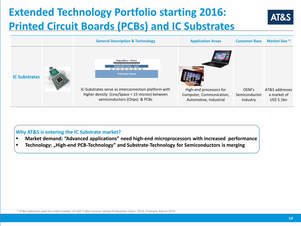
General Description & Technology Application Areas Customer Base Market Size *
IC Substrates
IC-Substrates serve as interconnection platform with higher density (Line/Space < 15 micron) between
semiconductors (Chips) & PCBs
High-end processors for Computer, Communication,
Automotive, Industrial
OEM’s Semiconductor
Industry
AT&S addresses a market of US$ 5.1bn
* AT&S addresses part of a total market of USD 7,6bn/ source: Global Production Value 2014, Prismark, March 2015
Extended Technology Portfolio starting 2016: Printed Circuit Boards (PCBs) and IC Substrates
Why AT&S is entering the IC Substrate market? Market demand: “Advanced applications” need high-end microprocessors with increased performance Technology: „High-end PCB-Technology” and Substrate-Technology for Semiconductors is merging
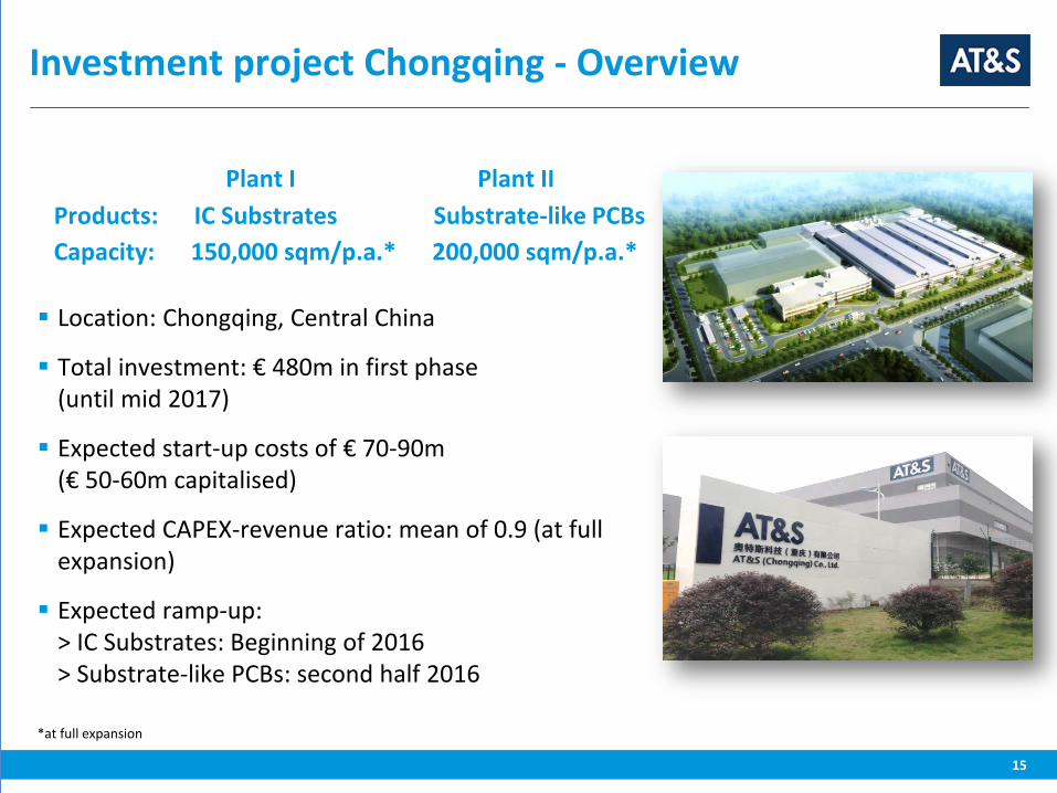
Investment project Chongqing - Overview
15
Location: Chongqing, Central China
Total investment: € 480m in first phase (until mid 2017)
Expected start-up costs of € 70-90m (€ 50-60m capitalised)
Expected CAPEX-revenue ratio: mean of 0.9 (at full expansion)
Expected ramp-up: > IC Substrates: Beginning of 2016 > Substrate-like PCBs: second half 2016
*at full expansion
Plant I Plant II Products: IC Substrates Substrate-like PCBs Capacity: 150,000 sqm/p.a.* 200,000 sqm/p.a.*
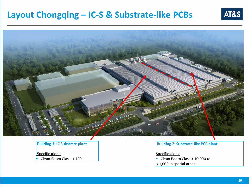
Layout Chongqing – IC-S & Substrate-like PCBs
Building 1: IC Substrate plant Specifications: Clean Room Class < 100
Building 2: Substrate-like PCB plant Specifications: Clean Room Class < 10,000 to < 1,000 in special areas
16
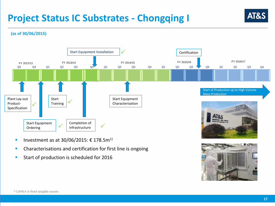
(as of 30/06/2015)
Completion of Infrastructure
Start Equipment Characterisation
Certification
Start Training
Start Equipment Ordering
Plant Lay-out Product- Specification
Start of Production up to High Volume Mass Production
17
Q4 Q1 Q2 Q3 FY 2013/14
Q4 Q1 Q2 Q3 FY 2014/15
Q3 FY 2012/13
Q4 Q1 Q2 Q3
FY 2015/16
Q4 Q1 Q2 Q3
FY 2016/17
Q4
Investment as at 30/06/2015: € 178.5m1)
Characterisations and certification for first line is ongoing
Start of production is scheduled for 2016
Project Status IC Substrates - Chongqing I
1) CAPEX in fixed tangible assets
Start Equipment Installation
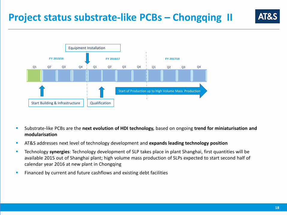
Substrate-like PCBs are the next evolution of HDI technology, based on ongoing trend for miniaturisation and modularisation
AT&S addresses next level of technology development and expands leading technology position
Technology synergies: Technology development of SLP takes place in plant Shanghai, first quantities will be available 2015 out of Shanghai plant; high volume mass production of SLPs expected to start second half of calendar year 2016 at new plant in Chongqing
Financed by current and future cashflows and existing debt facilities
18
Project status substrate-like PCBs – Chongqing II
Q4
Start Building & Infrastructure
Start of Production up to High Volume Mass Production
Q1 Q2 Q3
FY 2015/16
Q4 Q1 Q2 Q3
FY 2016/17 FY 2017/18
Q1 Q2 Q3 Q4
Equipment Installation
Qualification
19
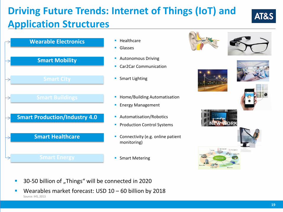
Driving Future Trends: Internet of Things (IoT) and Application Structures
Healthcare Glasses
Wearable Electronics
Smart Mobility Autonomous Driving
Car2Car Communication
Smart City Smart Lighting
Smart Buildings Home/Building Automatisation
Energy Management
Smart Production/Industry 4.0 Automatisation/Robotics
Production Control Systems
Smart Healthcare Connectivity (e.g. online patient monitoring)
Smart Energy Smart Metering
30-50 billion of „Things“ will be connected in 2020 Wearables market forecast: USD 10 – 60 billion by 2018
Source: IHS, 2013
20
Company Overview
Strategy & Market
Annex
Financials
Table of Contents
21
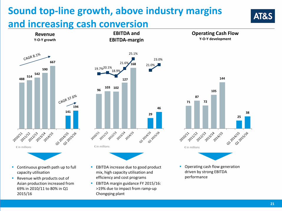
Sound top-line growth, above industry margins and increasing cash conversion
488 514
542 590
667
141 194
96 103 102
127
168
29
46
19.7% 20.1% 18.9%
21.6%
25.1%
21.0%
23.0%
€ in millions
71 87
72
105
144
25 38
Revenue Y-O-Y growth
Operating Cash Flow Y-O-Y development
EBITDA and EBITDA-margin
Continuous growth path up to full capacity utilisation
Revenue with products out of Asian production increased from 69% in 2010/11 to 80% in Q1 2015/16
EBITDA increase due to good product mix, high capacity utilisation and efficiency and cost programs
EBITDA margin guidance FY 2015/16: >19% due to impact from ramp-up Chongqing plant
Operating cash flow generation driven by strong EBITDA performance
€ in millions € in millions
Regular business
22
Capex & Staff
CAPEX CAPEX increase reflects technology investments in existing locations and investments in Chongqing project (whereof € 25.6m).
113
40
90
165
43 40
2011/12 2012/13 2013/14 2014/15 Q12014/15
Q12015/16
STAFF* The increased headcount is primarily based on the Chongqing project.
7,417 7,321 7,027 7,638
8,390
2011/12 2012/13 2013/14 2014/15 Q1 2015/16
123 609 54 1,049
* incl. leased personnel, FTE, average for the period (€ in millions)
Employees of project Chongqing
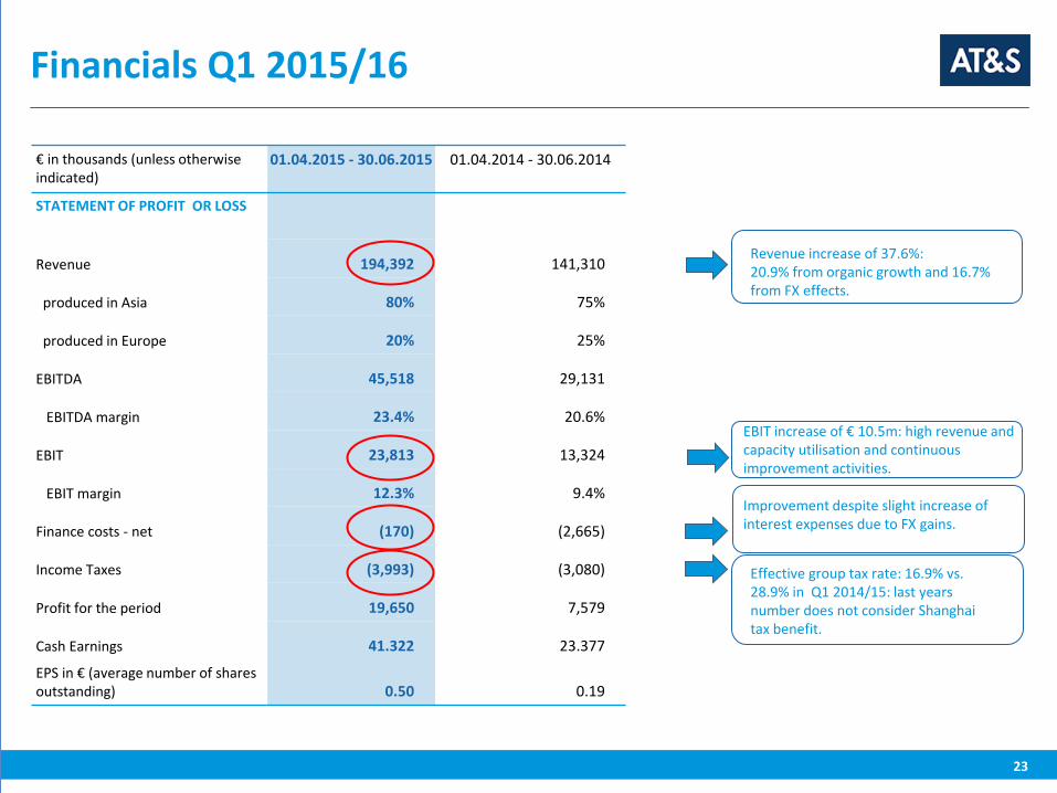
Financials Q1 2015/16
23
€ in thousands (unless otherwise indicated)
01.04.2015 - 30.06.2015 01.04.2014 - 30.06.2014
STATEMENT OF PROFIT OR LOSS
Revenue 194,392 141,310
produced in Asia 80% 75%
produced in Europe 20% 25%
EBITDA 45,518 29,131
EBITDA margin 23.4% 20.6%
EBIT 23,813 13,324
EBIT margin 12.3% 9.4%
Finance costs - net (170) (2,665)
Income Taxes (3,993) (3,080)
Profit for the period 19,650 7,579
Cash Earnings 41.322 23.377
EPS in € (average number of shares outstanding) 0.50 0.19
EBIT increase of € 10.5m: high revenue and capacity utilisation and continuous improvement activities.
Revenue increase of 37.6%: 20.9% from organic growth and 16.7% from FX effects.
Effective group tax rate: 16.9% vs. 28.9% in Q1 2014/15: last years number does not consider Shanghai tax benefit.
Improvement despite slight increase of interest expenses due to FX gains.
24
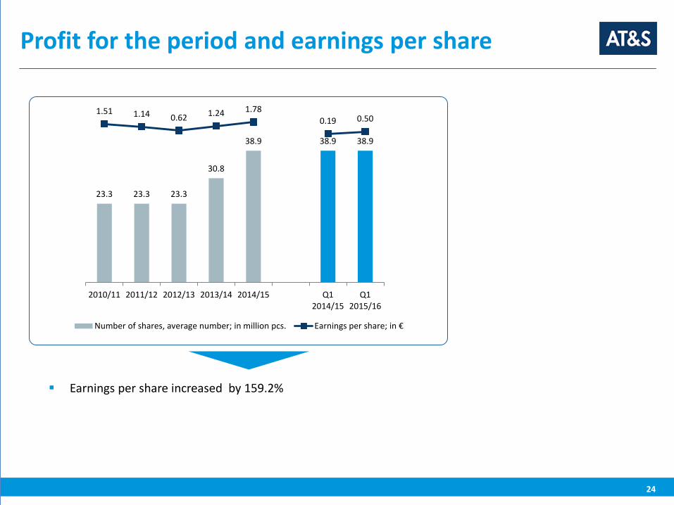
Profit for the period and earnings per share
Earnings per share increased by 159.2%
23.3 23.3 23.3
30.8
38.9 38.9 38.9
1.51 1.14 0.62 1.24 1.78 0.19 0.50
-20
-15
-10
-5
0
0
10
20
30
40
50
2010/11 2011/12 2012/13 2013/14 2014/15 Q12014/15
Q12015/16
Number of shares, average number; in million pcs. Earnings per share; in €
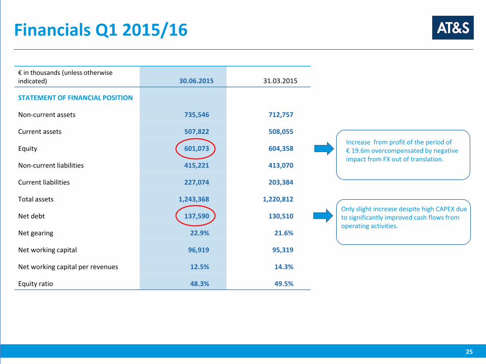
Financials Q1 2015/16
25
€ in thousands (unless otherwise indicated) 30.06.2015 31.03.2015
STATEMENT OF FINANCIAL POSITION
Non-current assets 735,546 712,757
Current assets 507,822 508,055
Equity 601,073 604,358
Non-current liabilities 415,221 413,070
Current liabilities 227,074 203,384
Total assets 1,243,368 1,220,812
Net debt 137,590 130,510
Net gearing 22.9% 21.6%
Net working capital 96,919 95,319
Net working capital per revenues 12.5% 14.3%
Equity ratio 48.3% 49.5%
Increase from profit of the period of € 19.6m overcompensated by negative impact from FX out of translation.
Only slight increase despite high CAPEX due to significantly improved cash flows from operating activities.
26
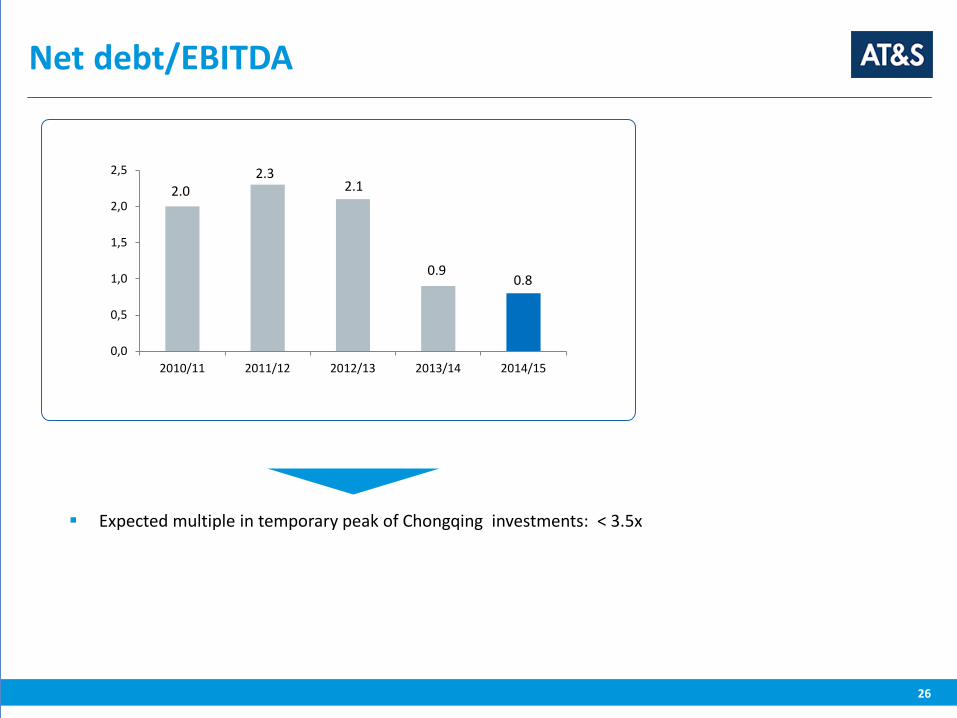
Net debt/EBITDA
0,0
0,5
1,0
1,5
2,0
2,5
2010/11 2011/12 2012/13 2013/14 2014/15
2.3 2.0 2.1
0.9 0.8
Expected multiple in temporary peak of Chongqing investments: < 3.5x
27
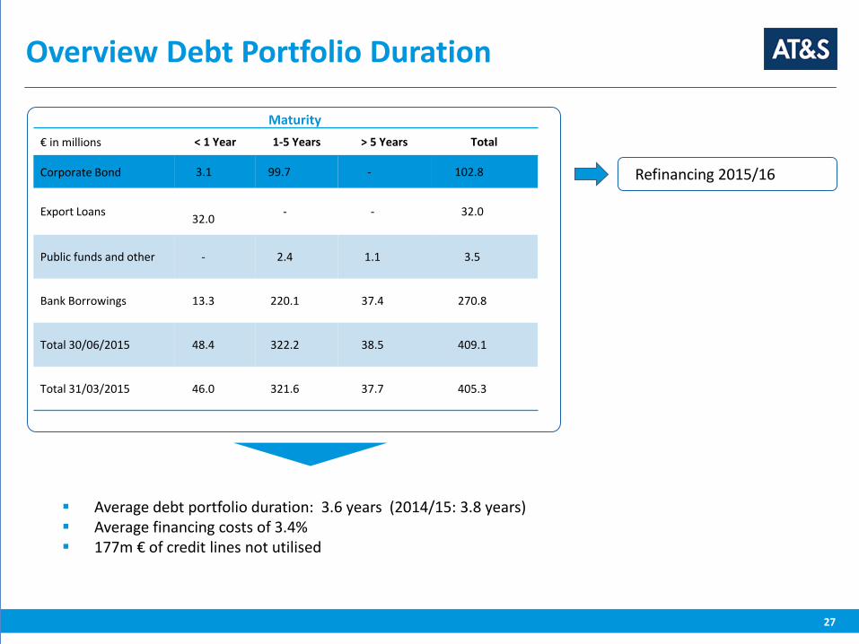
Overview Debt Portfolio Duration
Maturity € in millions < 1 Year 1-5 Years > 5 Years Total
Corporate Bond 3.1 99.7 - 102.8
Export Loans 32.0 - - 32.0
Public funds and other - 2.4 1.1 3.5
Bank Borrowings 13.3 220.1 37.4 270.8
Total 30/06/2015 48.4 322.2 38.5 409.1
Total 31/03/2015 46.0 321.6 37.7 405.3
Average debt portfolio duration: 3.6 years (2014/15: 3.8 years) Average financing costs of 3.4% 177m € of credit lines not utilised
Refinancing 2015/16
Financials Q1 2015/16
28
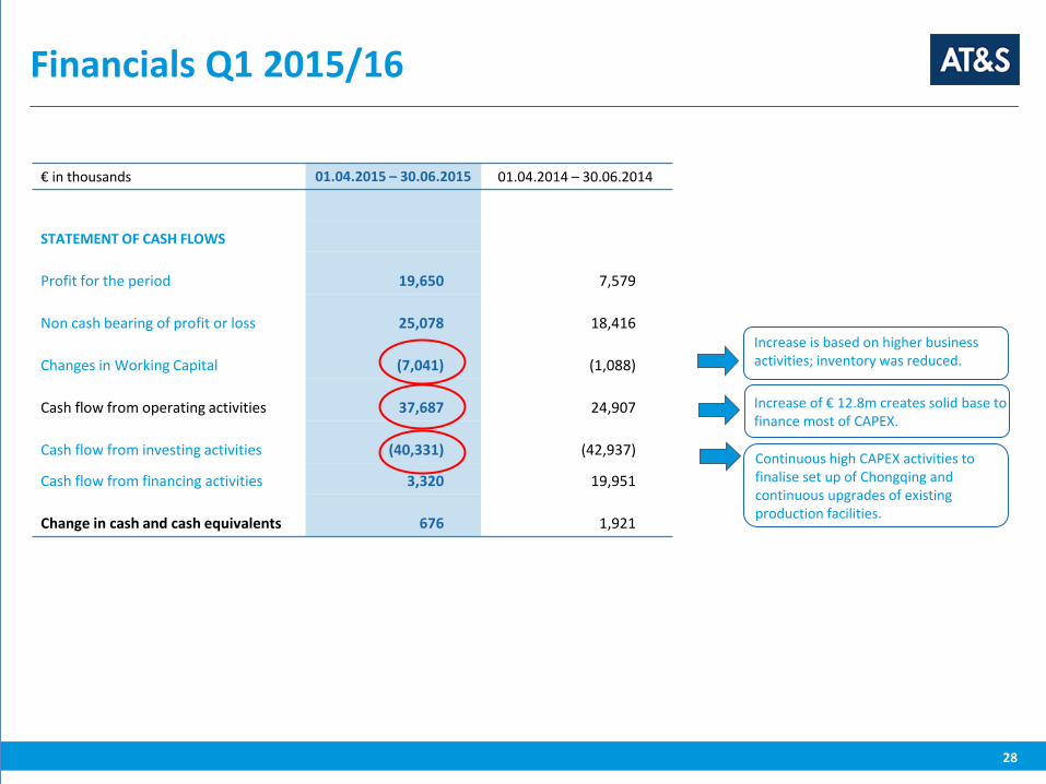
€ in thousands 01.04.2015 – 30.06.2015 01.04.2014 – 30.06.2014)
STATEMENT OF CASH FLOWS
Profit for the period 19,650 7,579
Non cash bearing of profit or loss 25,078 18,416
Changes in Working Capital (7,041) (1,088)
Cash flow from operating activities 37,687 24,907
Cash flow from investing activities (40,331) (42,937)
Cash flow from financing activities 3,320 19,951
Change in cash and cash equivalents 676 1,921
Increase is based on higher business activities; inventory was reduced. Increase of € 12.8m creates solid base to finance most of CAPEX.
Continuous high CAPEX activities to finalise set up of Chongqing and continuous upgrades of existing production facilities.
29
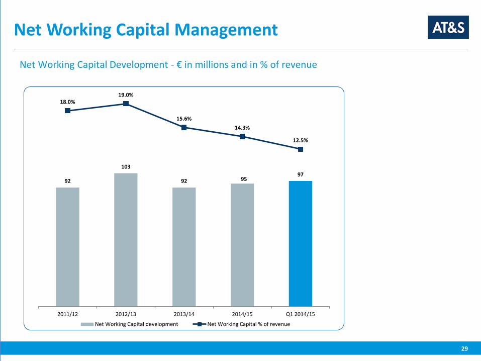
Net Working Capital Management
Net Working Capital Development - € in millions and in % of revenue
92
103
92 95 97
18.0% 19.0%
15.6% 14.3%
12.5%
2011/12 2012/13 2013/14 2014/15 Q1 2014/15
Net Working Capital development Net Working Capital % of revenue
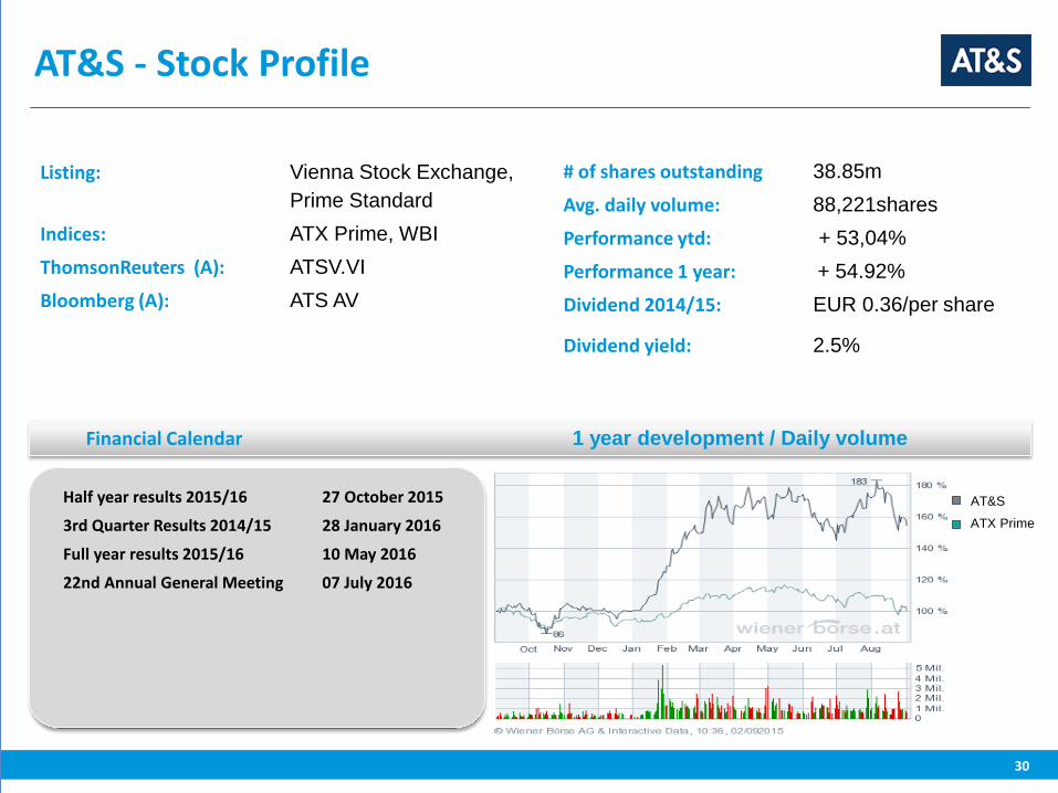
AT&S - Stock Profile
Listing: Vienna Stock Exchange, Prime Standard
Indices: ATX Prime, WBI ThomsonReuters (A): ATSV.VI Bloomberg (A): ATS AV
Half year results 2015/16 27 October 2015
3rd Quarter Results 2014/15 28 January 2016
Full year results 2015/16 10 May 2016
22nd Annual General Meeting 07 July 2016
30
Financial Calendar 1 year development / Daily volume
ATX Prime
AT&S
# of shares outstanding 38.85m Avg. daily volume: 88,221shares Performance ytd: + 53,04% Performance 1 year: + 54.92% Dividend 2014/15: EUR 0.36/per share
Dividend yield: 2.5%
31
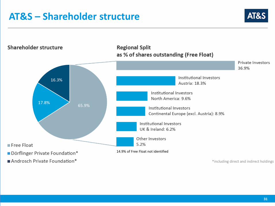
14.9% of Free Float not identified
AT&S – Shareholder structure
32
Outlook FY 2015/16
Provided a stable macroeconomic environment and continuous good customer demand Management expects an ongoing high level of capacity utilisation.
On the basis of the organic growth of the first quarter, a business development at the level of the previous year in the next three quarters and an average USD-EUR exchange rate of 1.19, the Management Board has increased the revenue expected for the financial year 2015/16 to € 725m.
Influenced by the expected costs of the start-up of the new plants in Chongqing, the EBITDA margin should exceed 19% (guidance at the beginning of the financial year: 18-20%). This includes an EBITDA margin in the core business at the level of the previous year.
33
Company Overview
Strategy & Market
Annex
Financials
Table of Contents
34
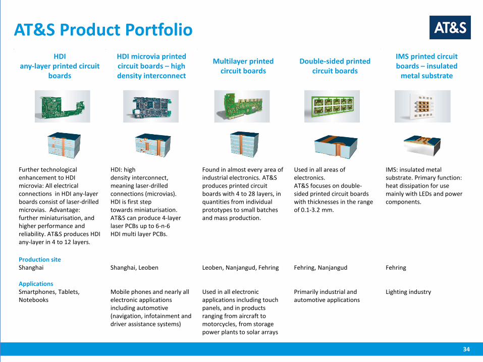
AT&S Product Portfolio HDI
any-layer printed circuit boards
HDI microvia printed circuit boards – high density interconnect
Multilayer printed circuit boards
Double-sided printed circuit boards
IMS printed circuit boards – insulated
metal substrate
Further technological enhancement to HDI microvia: All electrical connections in HDI any-layer boards consist of laser-drilled microvias. Advantage: further miniaturisation, and higher performance and reliability. AT&S produces HDI any-layer in 4 to 12 layers.
HDI: high density interconnect, meaning laser-drilled connections (microvias). HDI is first step towards miniaturisation. AT&S can produce 4-layer laser PCBs up to 6-n-6 HDI multi layer PCBs.
Found in almost every area of industrial electronics. AT&S produces printed circuit boards with 4 to 28 layers, in quantities from individual prototypes to small batches and mass production.
Used in all areas of electronics. AT&S focuses on double-sided printed circuit boards with thicknesses in the range of 0.1-3.2 mm.
IMS: insulated metal substrate. Primary function: heat dissipation for use mainly with LEDs and power components.
Production site Shanghai
Shanghai, Leoben
Leoben, Nanjangud, Fehring
Fehring, Nanjangud
Fehring
Applications Smartphones, Tablets, Notebooks
Mobile phones and nearly all electronic applications including automotive (navigation, infotainment and driver assistance systems)
Used in all electronic applications including touch panels, and in products ranging from aircraft to motorcycles, from storage power plants to solar arrays
Primarily industrial and automotive applications
Lighting industry
35
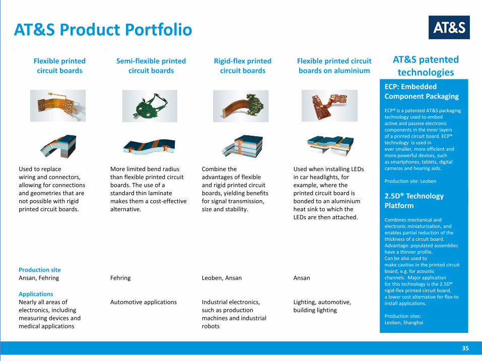
AT&S Product Portfolio Flexible printed circuit boards
Semi-flexible printed circuit boards
Rigid-flex printed circuit boards
Flexible printed circuit boards on aluminium
AT&S patented technologies
Used to replace wiring and connectors, allowing for connections and geometries that are not possible with rigid printed circuit boards.
More limited bend radius than flexible printed circuit boards. The use of a standard thin laminate makes them a cost-effective alternative.
Combine the advantages of flexible and rigid printed circuit boards, yielding benefits for signal transmission, size and stability.
Used when installing LEDs in car headlights, for example, where the printed circuit board is bonded to an aluminium heat sink to which the LEDs are then attached.
Production site Ansan, Fehring
Fehring
Leoben, Ansan
Ansan
Applications Nearly all areas of electronics, including measuring devices and medical applications
Automotive applications
Industrial electronics, such as production machines and industrial robots
Lighting, automotive, building lighting
ECP: Embedded Component Packaging ECP® is a patented AT&S packaging technology used to embed active and passive electronic components in the inner layers of a printed circuit board. ECP® technology is used in ever smaller, more efficient and more powerful devices, such as smartphones, tablets, digital cameras and hearing aids. Production site: Leoben
2.5D® Technology Platform Combines mechanical and electronic miniaturisation, and enables partial reduction of the thickness of a circuit board. Advantage: populated assemblies have a thinner profile. Can be also used to make cavities in the printed circuit board, e.g. for acoustic channels. Major application for this technology is the 2.5D® rigid-flex printed circuit board, a lower cost alternative for flex-to install applications. Production sites: Leoben, Shanghai
Management
36
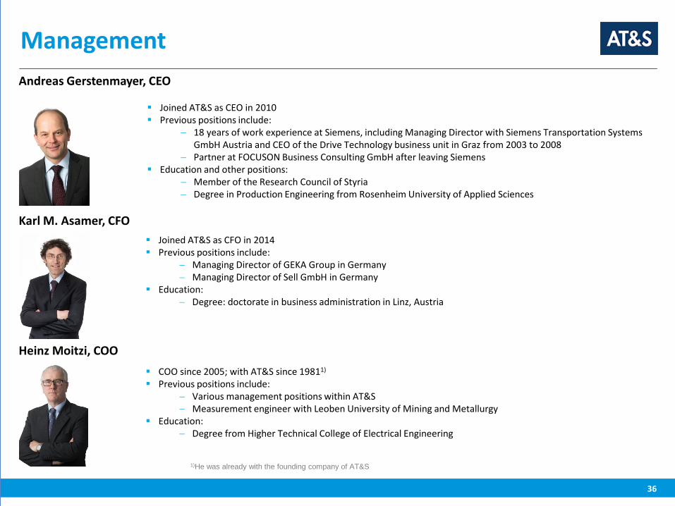
Andreas Gerstenmayer, CEO
Joined AT&S as CEO in 2010 Previous positions include:
− 18 years of work experience at Siemens, including Managing Director with Siemens Transportation Systems GmbH Austria and CEO of the Drive Technology business unit in Graz from 2003 to 2008
− Partner at FOCUSON Business Consulting GmbH after leaving Siemens Education and other positions:
− Member of the Research Council of Styria − Degree in Production Engineering from Rosenheim University of Applied Sciences
Heinz Moitzi, COO COO since 2005; with AT&S since 19811) Previous positions include:
− Various management positions within AT&S − Measurement engineer with Leoben University of Mining and Metallurgy
Education: − Degree from Higher Technical College of Electrical Engineering
Karl M. Asamer, CFO Joined AT&S as CFO in 2014 Previous positions include:
− Managing Director of GEKA Group in Germany − Managing Director of Sell GmbH in Germany
Education: − Degree: doctorate in business administration in Linz, Austria
1)He was already with the founding company of AT&S
37
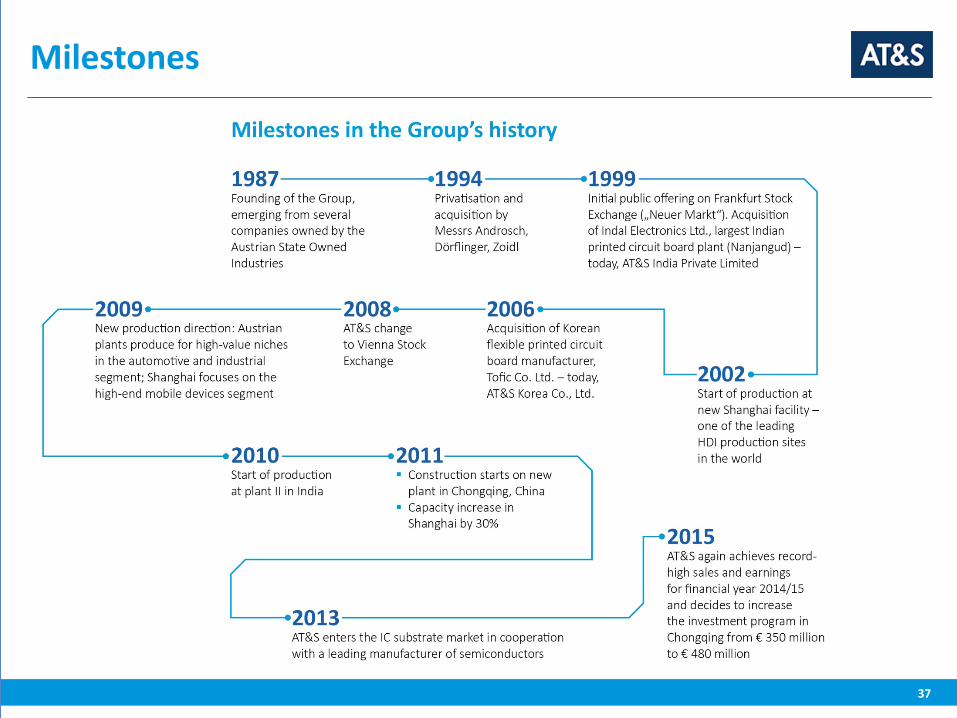
Milestones
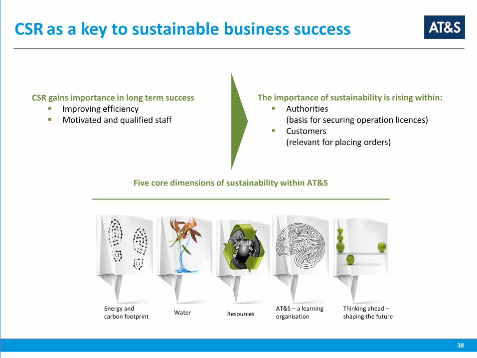
Five core dimensions of sustainability within AT&S
Energy and carbon footprint
Water AT&S – a learning organisation
Resources
Thinking ahead – shaping the future
CSR gains importance in long term success Improving efficiency Motivated and qualified staff
CSR as a key to sustainable business success
38
The importance of sustainability is rising within:
Authorities (basis for securing operation licences)
Customers (relevant for placing orders)
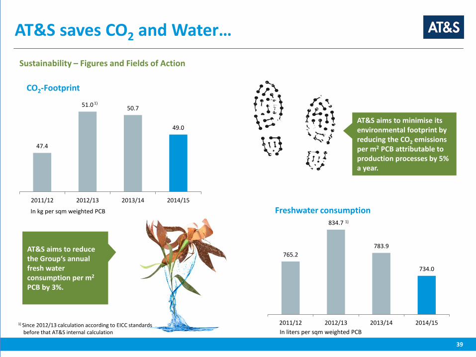
AT&S saves CO2 and Water…
39
Sustainability – Figures and Fields of Action
AT&S aims to minimise its environmental footprint by reducing the CO2 emissions per m2 PCB attributable to production processes by 5% a year.
AT&S aims to reduce the Group‘s annual fresh water consumption per m2
PCB by 3%.
765.2
834.7
783.9
734.0
2011/12 2012/13 2013/14 2014/15
Freshwater consumption
In liters per sqm weighted PCB
1)
47.4
51.0 50.7
49.0
2011/12 2012/13 2013/14 2014/15
CO2-Footprint 1)
In kg per sqm weighted PCB
1) Since 2012/13 calculation according to EICC standards before that AT&S internal calculation
Visit: www.ats.net; Twitter @AT&S IR_PR; YouTube AtundS
40
AT&S – first choice for advanced applications
IR Contact: Elke Koch Fabriksgasse 13, 8700 Leoben/Austria Tel: +43 3842 200 5925 Mobile: +43 676 8955 5925 Fax: +43 3842 200 15909 [email protected] www.ats.net
Disclaimer
41
This presentation is provided by AT & S Austria Technologie & Systemtechnik Aktiengesellschaft, having its headquarter at Fabriksgasse 13, 8700 Leoben, Austria (“AT&S”), and the contents are proprietary to AT&S and for information only.
AT&S does not provide any representations or warranties with regard to this presentation or for the correctness and completeness of the statements contained therein, and no reliance may be placed for any purpose whatsoever on the information contained in this presentation, which has not been independently verified. You are expressly cautioned not to place undue reliance on this information.
This presentation may contain forward-looking statements which were made on the basis of the information available at the time of preparation and on management‘s expectations and assumptions. However, such statements are by their very nature subject to known and unknown risks and uncertainties. As a result, actual developments, results, performance or events may vary significantly from the statements contained explicitly or implicitly herein.
Neither AT&S, nor any affiliated company, or any of their directors, officers, employees, advisors or agents accept any responsibility or liability (for negligence or otherwise) for any loss whatsoever out of the use of or otherwise in connection with this presentation. AT&S undertakes no obligation to update or revise any forward-looking statements, whether as a result of changed assumptions or expectations, new information or future events.
This presentation does not constitute a recommendation, an offer or invitation, or solicitation of an offer, to subscribe for or purchase any securities, and neither this presentation nor anything contained herein shall form the basis of any contract or commitment whatsoever. This presentation does not constitute any financial analysis or financial research and may not be construed to be or form part of a prospectus. This presentation is not directed at, or intended for distribution to or use by, any person or entity that is a citizen or resident or located in any locality, state, country or other jurisdiction where such distribution, publication, availability or use would be contrary to law or regulation or which would require any registration or licensing within such jurisdiction.