Embed Size (px)
Citation preview

Research ArticleOptimization of the Electrodeposition Parameters toImprove the Stoichiometry of In2S3 Films for Solar ApplicationsUsing the Taguchi Method
Maqsood Ali Mughal1 M Jason Newell1 Joshua Vangilder1 Shyam Thapa1 Kayla Wood2
Robert Engelken12 B Ross Carroll3 and J Bruce Johnson3
1 Environmental Sciences Graduate Program Arkansas State University State University Jonesboro AR 72467 USA2 Electrical Engineering Program Arkansas State University State University Jonesboro AR 72467 USA3 Chemistry and Physics Program Arkansas State University State University Jonesboro AR 72467 USA
Correspondence should be addressed to Robert Engelken bdengensastateedu
Received 7 November 2013 Accepted 28 March 2014 Published 30 April 2014
Academic Editor Alireza Talebitaher
Copyright copy 2014 Maqsood Ali Mughal et al This is an open access article distributed under the Creative Commons AttributionLicense which permits unrestricted use distribution and reproduction in any medium provided the original work is properlycited
Properties of electrodeposited semiconductor thin films are dependent upon the electrolyte composition plating time andtemperature as well as the current density and the nature of the substrate In this study the influence of the electrodepositionparameters such as deposition voltage deposition time composition of solution and deposition temperature upon the propertiesof In2S3films was analyzed by the Taguchi Method According to Taguchi analysis the interaction between deposition voltage and
deposition time was significant Deposition voltage had the largest impact upon the stoichiometry of In2S3films and deposition
temperature had the least impact The stoichiometric ratios between sulfur and indium (SIn 32) obtained from experimentsperformed with optimized electrodeposition parameters were in agreement with predicted values from the Taguchi Method Theexperiments were carried out according to Taguchi orthogonal array L
27(34) design of experiments (DOE) Approximately 600 nm
thick In2S3films were electrodeposited from an organic bath (ethylene glycol-based) containing indium chloride (InCl
3) sodium
chloride (NaCl) and sodium thiosulfate (Na2S2O3sdot5H2O) the latter used as an additional sulfur source along with elemental sulfur
(S) An X-ray diffractometer (XRD) energy dispersive X-ray spectroscopy (EDS) unit and scanning electron microscope (SEM)were respectively used to analyze the phases elemental composition and morphology of the electrodeposited In
2S3films
1 Introduction
During the last few decades solar energy has receivedattention due to increased environmental concerns overtraditional energy resources such as coal oil and natural gasFossil fuel prices will rise over time and resources may even-tually deplete Hence the worldrsquos current electricity supplyis facing government businesses and consumer pressures tosupport development of alternative energy resources such assolar cells The solar industry has come of age lately and theworldrsquos most efficient solar cell from Sharp can convert animpressive 444 of incoming photon energy into electricalenergy [1] Prices of solar panels have continued to dropwhile the market size of the US solar industry grew 34between 2011 ($86 billion 1187MW) and 2013 ($115 billion
3317MW) [2] However scientists continue to research novelsemiconductor materials and deposition techniques that canprovide higher efficiencies and low-cost solar panels with lessenvironmental impact upon the Earth
In this paper we report studies on electrodeposition ofIn2S3 an environmentally friendly replacement to CdS for
solar cell applications as a buffer layer In2S3films were
electrodeposited onto molybdenum-coated glass substratesElectrodeposition is a low-cost nonvacuum and large indus-trial scale-based deposition technique to deposit materialefficiently and uniformly However the electrochemistrybehind it is complex due to multiple deposition parametersthat may have individually and in tandem an impact uponthe properties of the material [3 4]The Taguchi Method wasused to optimize electrodeposition parameters in order to
Hindawi Publishing CorporationJournal of NanomaterialsVolume 2014 Article ID 302159 10 pageshttpdxdoiorg1011552014302159
2 Journal of Nanomaterials
improve the stoichiometry of In2S3films which is one of the
most important properties of any photovoltaic material andcritical to obtaining the desired band gap and performanceTherefore in the present study the primary goal was toimprove the stoichiometrywhile avoiding nonuniformity andnonadherency in the electrodeposited In
2S3films Taguchi
analysis helped us to analyze the effect of each depositionparameter upon the stoichiometry of In
2S3films
2 Materials and Methods
21 Indium Sulfide (In2S3) In2S3is an important member of
IIIndashVI group of midgap semiconducting sulfides applicablefor optoelectronics solar cells and photoelectric devices [2]In2S3is an indirect band gap semiconductor with potential
to become a nontoxic alternative to CdS as a buffer layer incopper indium gallium selenidesulfide- (CIGS-) based solarcells [5 6] It is a promising buffer material for photovoltaicapplications because of its stability reasonably wide band gap(23 eV) [7 8] and photoconductive behavior [9] Severalreports have been published on deposition of In
2S3by
different deposition techniques (both wet and dry) in thinfilm and powder form with diverse morphologies [7 10 11]In CIGS-based solar cells buffered with In
2S3 efficiencies of
157 [12] have been achieved which is slightly less than the16 efficiency reported for CdS-based solar cells depositedby chemical bath deposition (CBD) [13] ElectrodepositedIn2S3-buffered CIGSe solar cells have yielded 102 efficiency
[14] However the use of ethylene glycol as an organicelectrolyte for the electrochemical synthesis of In
2S3films
has not been reported previously with the exception ofIEEE conference proceedings [3] regarding our work atthe Optoelectronic Materials Research Laboratory (OMRL)Arkansas State University Jonesboro AR
22 Electrodeposition Electrodeposition is widely used inthe coating industry and is considered to be a low-costtechnique for large surface coatings with full coverage andhigh growth yield [15] It was introduced by Kroger in thefield of semiconductors in 1978 while working on cathodicdeposition of CdTe an absorber material [16] Since thenelectrodeposition has emerged as a method for the synthesisof semiconductor thin films and manufacturing of nanos-tructures such as chalcogenides [17] Electrodeposition takesplacewhen voltage is applied across the electrodes (anode andcathode) immersed in an electrolyte The anode is anodizedand the cations in the solution start moving towards thecathode with the help of the electric field created in theelectrochemical cell The reduction reaction takes place atthe surface of the cathode and leads to deposition of thedesired material The process provides high material trans-ferutilization efficiency in situmeasurements [18] precisioncontrol with proper bath chemistry and environmental safetyin terms of solvent emissions [14] However most of thework on semiconductor electrodeposition is limited to a fewtechnologically important semiconductors There are severaldeposition parameters which can affect the properties of thesemiconductor material [19] Many fundamental aspects of
the electrodeposition of semiconductors are still misunder-stood and not clearly defined Since In
2S3shows promise and
has not been studied as extensively as some semiconductorsin this work we determine the optimal deposition parametersfor the electrodeposition of In
2S3thin films to obtain proper
stoichiometry crystalline structure and morphology
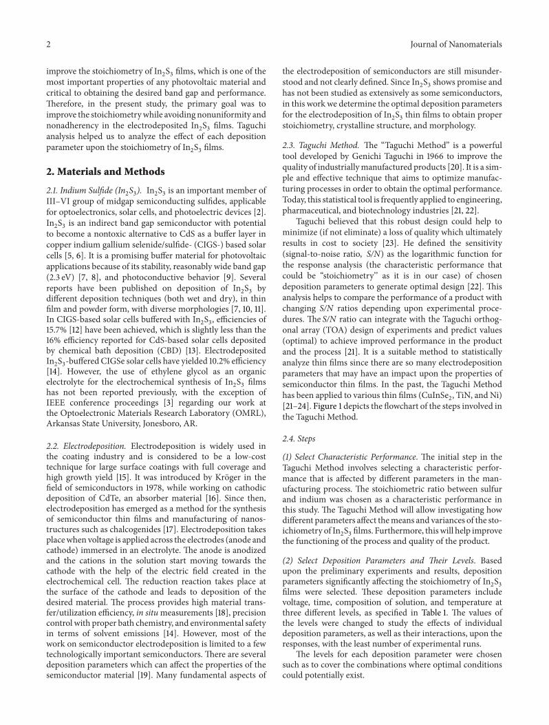
23 Taguchi Method The ldquoTaguchi Methodrdquo is a powerfultool developed by Genichi Taguchi in 1966 to improve thequality of industriallymanufactured products [20] It is a sim-ple and effective technique that aims to optimize manufac-turing processes in order to obtain the optimal performanceToday this statistical tool is frequently applied to engineeringpharmaceutical and biotechnology industries [21 22]
Taguchi believed that this robust design could help tominimize (if not eliminate) a loss of quality which ultimatelyresults in cost to society [23] He defined the sensitivity(signal-to-noise ratio SN) as the logarithmic function forthe response analysis (the characteristic performance thatcould be ldquostoichiometryrsquorsquo as it is in our case) of chosendeposition parameters to generate optimal design [22] Thisanalysis helps to compare the performance of a product withchanging SN ratios depending upon experimental proce-dures The SN ratio can integrate with the Taguchi orthog-onal array (TOA) design of experiments and predict values(optimal) to achieve improved performance in the productand the process [21] It is a suitable method to statisticallyanalyze thin films since there are so many electrodepositionparameters that may have an impact upon the properties ofsemiconductor thin films In the past the Taguchi Methodhas been applied to various thin films (CuInSe
2 TiN and Ni)
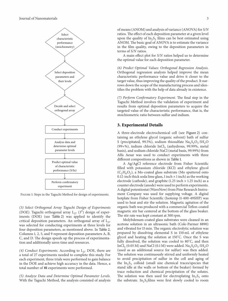
[21ndash24] Figure 1 depicts the flowchart of the steps involved inthe Taguchi Method
24 Steps
(1) Select Characteristic Performance The initial step in theTaguchi Method involves selecting a characteristic perfor-mance that is affected by different parameters in the man-ufacturing process The stoichiometric ratio between sulfurand indium was chosen as a characteristic performance inthis study The Taguchi Method will allow investigating howdifferent parameters affect themeans and variances of the sto-ichiometry of In
2S3films Furthermore thiswill help improve
the functioning of the process and quality of the product
(2) Select Deposition Parameters and Their Levels Basedupon the preliminary experiments and results depositionparameters significantly affecting the stoichiometry of In
2S3
films were selected These deposition parameters includevoltage time composition of solution and temperature atthree different levels as specified in Table 1 The values ofthe levels were changed to study the effects of individualdeposition parameters as well as their interactions upon theresponses with the least number of experimental runs
The levels for each deposition parameter were chosensuch as to cover the combinations where optimal conditionscould potentially exist
Journal of Nanomaterials 3
Selectcharacteristicperformance
(stoichiometry)
Select depositionparameters and
their levels
Decide and selectorthogonal array
Conduct experiments
Analyze data anddetermine optimal
parameter levels
Predict optimal valueof characteristic
performance (SIn)
Perform confirmatoryexperiment
Figure 1 Steps in the Taguchi Method for design of experiments
(3) Select Orthogonal Array Taguchi Design of Experiments(DOE) Taguchi orthogonal array L
27(34) design of exper-
iments (DOE) (see Table 2) was applied to identify thecritical deposition parameters An orthogonal array of L
27
was selected for conducting experiments at three levels forfour deposition parameters as mentioned above In Table 2Columns 1 2 5 and 9 represent deposition parameters A BC and D The design speeds up the process of experimenta-tion and additionally saves time and resources
(4) Conduct Experiments According to L27
DOE there area total of 27 experiments needed to complete this study Foreach experiment three trials were performed to gain balancein the DOE and achieve high accuracy in the data Hence atotal number of 81 experiments were performed
(5) Analyze Data and Determine Optimal Parameter LevelsWith the Taguchi Method the analysis consisted of analysis
ofmeans (ANOM) and analysis of variance (ANOVA) for SNratiosThe effect of each deposition parameter at a given levelupon the quality of In
2S3films can be best estimated using
ANOMThe basic goal of ANOVA is to estimate the variancein the film quality owing to the deposition parameters interms of SN ratios
A main effect plot for SN ratios helped us to determinethe optimal value for each deposition parameter
(6) Predict Optimal Values Orthogonal Regression AnalysisOrthogonal regression analysis helped improve the meancharacteristic performance value and drive it closer to thetarget value thus improving the quality of the product It nar-rows down the scope of the manufacturing process and iden-tifies the problem with the help of data already in existence
(7) Perform Confirmatory Experiment The final step in theTaguchi Method involves the validation of experiment andresults from optimal deposition parameters to acquire thetargeted value of the characteristic performance that is thestoichiometric ratio between sulfur and indium
3 Experimental Details
A three-electrode electrochemical cell (see Figure 2) con-taining an ethylene glycol (organic solvent) bath of sulfurS (precipitated 995) sodium thiosulfate Na
2S2O3sdot5H2O
(99+) indium chloride InCl3(anhydrous 9999 metal
basis) and sodium chloride NaCl (metal basis 9999) fromAlfa Aesar was used to conduct experiments with threedifferent compositions as shown in Table 1
A AgAgCl reference electrode from Fisher Scientificfilled with potassium chloride (KCl) and ethylene glycol(C2H6O2) a Mo-coated glass substrate (Mo sputtered onto
012-inch thick soda lime glass 1 inch times 1 inch) as the workingelectrode (cathode) and graphite (125 inch times 125 inch) as acounter electrode (anode) were used to perform experimentsA digital potentiostat (WaveNow) fromPine Research Instru-ment Company was used for supplying voltage A digitalhotplate from Fisher Scientific (Isotemp 11-400-49SHP) wasused to heat and stir the solution Magnetic agitation of theorganic bath was produced with a commercial Teflon-coatedmagnetic stir bar centered at the bottom of the glass beakerThe stir rate was kept constant at 300 rpm
Molybdenum-coated glass substrates were cleaned in anacetone solution in an ultrasonic bath (Cole-Parmer 8890)and vibrated for 15minThe organic electrolytic solution wasprepared by dissolving elemental S in 150mL of ethyleneglycol and heating the solution at 150∘C Once the S wasfully dissolved the solution was cooled to 80∘C and thenInCl3(005M) and NaCl (01M) were added Na
2S2O3sdot5H2O
(used as an additional source for sulfur) was then addedThe solution was continuously stirred and uniformly heatedto avoid precipitation of sulfur in the cell and aging ofthe In
2S3colloid (small size chemical tracesspecies that
stand idle at the walls or bottom of the beaker) formed bytrace reduction and chemical precipitation of the solutesThe solution was then used for electroplating In
2S3onto
the substrate In2S3films were first slowly cooled to room
4 Journal of Nanomaterials
Table 1 Control deposition parameters and levels for the electrodeposition of In2S3 thin films
Level ldquo119860rdquo depositionvoltage (V)
ldquo119861rdquo deposition time(min) ldquo119862rdquo composition of solution ldquo119863rdquo deposition
temperature (∘C)1 minus06 3 01M S + 005M InCl3 + 01MNaCl 150
2 minus07 601M S + 01MNa2S2O3sdot5H2O +
005M InCl3 + 01MNaCl 160
3 minus08 9 02MS + 005M InCl3 + 01MNaCl 170
Table 2 Taguchi orthogonal array L27 (34) design of experiments with interactions
Exp number 1 (119860) 2 (119861) 3(119860 times 119861)
4(119860 times 119861) 5 (119862) 6
(119860 times 119862)7
(119860 times 119862)8
(119861 times 119862) 9 (119863) 10 11(119861 times 119862) 12 13
1 1 1 1 1 1 1 1 1 1 1 1 1 12 1 1 1 1 2 2 2 2 2 2 2 2 23 1 1 1 1 3 3 3 3 3 3 3 3 34 1 2 2 2 1 1 1 2 2 2 3 3 35 1 2 2 2 2 2 2 3 3 3 1 1 16 1 2 2 2 3 3 3 1 1 1 2 2 27 1 3 3 3 1 1 1 3 3 3 2 2 28 1 3 3 3 2 2 2 1 1 1 3 3 39 1 3 3 3 3 3 3 2 2 2 1 1 110 2 1 2 3 1 2 3 1 2 3 1 2 311 2 1 2 3 2 3 1 2 3 1 2 3 112 2 1 2 3 3 1 2 3 1 2 3 1 213 2 2 3 1 1 2 3 2 3 1 3 1 214 2 2 3 1 2 3 1 3 1 2 1 2 315 2 2 3 1 3 1 2 1 2 3 2 3 116 2 3 1 2 1 2 3 3 1 2 2 3 117 2 3 1 2 2 3 1 1 2 3 3 1 218 2 3 1 2 3 1 2 2 3 1 1 2 319 3 1 3 2 1 3 2 1 3 2 1 3 220 3 1 3 2 2 1 3 2 1 3 2 1 321 3 1 3 2 3 2 1 3 2 1 3 2 122 3 2 1 3 1 3 2 2 1 3 3 2 123 3 2 1 3 2 1 3 3 2 1 1 3 224 3 2 1 3 3 2 1 1 3 2 2 1 325 3 3 2 1 1 3 2 3 2 1 2 1 326 3 3 2 1 2 1 3 1 3 2 3 2 127 3 3 2 1 3 2 1 2 1 3 1 3 2
temperature to avoid thermal shock by immersing in warmedethylene glycol and then rinsed with distilled water andacetone The samples were stored in airtight plastic boxes
4 Results and Discussions
41 Energy Dispersive X-Ray Spectroscopy (EDS) After con-ducting all 81 experiments the elemental compositions forthe electrodeposited In
2S3films were determined using EDS
on the scanning electron microscope (SEM) from Tescan(Model VEGATS 5136XM)The INCAX-Sight (Model 7378)fromOxford Instruments is integrated with the SEM for EDS
to function The films were scratched off of the Mo-coatedglass substrates because sulfur peaks (K lines) in EDS overlapwith molybdenum peaks (L lines) from the substrates duringacquisition at about 23 keV
Following removal the film was collected on an alu-minum stub in powder form with the help of adhesive tabsEDS was performed on three different areas over the surfacedistribution of the scratched-In
2S3film collected on the stub
to calculate the mean SIn molar ratio for each film (seeFigure 3 and Table 3) The In
2S3films may contain oxygen
carbon aluminum and molybdenum as is evident fromTable 3 (see Spectra 1 and 2) The In
2S3films may oxidize
Journal of Nanomaterials 5
Temperature
Workingelectrode
Counterelectrode
Referenceelectrode
Aerial view
Side view
probe
Figure 2 Three-electrode electrochemical cell
Table 3 EDS analysis (Experiment Number 5 Trial 2)
Spectrum Atomic O C S Mo Al In SIn
Spectrum 1 167 2127 3741 0 0 2462 1519Spectrum 2 105 20 4445 321 0 3129 1421Spectrum 3 0 0 6032 0 0 3968 1520Mean 591 1375 4739 107 0 3186 1487
over a period of time especially if not properlyimmediatelystored Since the adhesive on the aluminum stub used tocollect the scratched-In
2S3film contains carbon EDS may
detect carbon and also aluminum as a part of the compo-sition of the film Molybdenummay also be detected by EDSas films were scratched off of the molybdenum-coated glasssubstrate However the stoichiometric ratios between sulfurand indiumwere close to optimal values which is also evidentfrom Table 3
Hence the SIn ratio calculated for each experiment wasthe mean of the mean SIn ratios determined from all threetrials for the same experiment The SIn ratios determinedfor all 27 experiments are listed in Table 4
42 Signal-to-Noise Ratio (SN) Analysis Signal-to-noiseratio (SN) was calculated using Minitab 16 in response tothese stoichiometric ratios to measure the quality character-istic The average SN ratio was an average of all SN ratios ofa deposition parameter at a given level
The formula used to calculate the SN ratio is given by thefollowing equation (ldquo119910rdquo is the mean value of the performancecharacteristic for a given experiment and ldquo119904rdquo is the variance)
119878119873 = 10 log1199102
119894
1199042
119894
(1)
SEM MAG 121 kx DET SE detector
50120583m
HV 100 kV Date 041113
(a)
DET SE detectorSEM MAG 99x
Spectrum 1
Spectrum 2
Spectrum 3
2mm
Date 041113HV 20kV
(b)
Figure 3 E52 (ExperimentNumber 5 andTrialNumber 2) (a) SEMimage of In
2S3film at 121 kX (b) SEM image of scratched off film on
an aluminum stub at 99X with selected surface area (squares) forEDS analysis
where
1199042
119894=1
119873119894minus 1
119873119894
sum
119906=1
(119910119894119906minus 119910119894) (2)
119910119894=1
119873119894
119873119894
sum
119906=1
119910119894119906 (3)
where 119894 is the experiment number 119906 is the trial number and119873119894is the number of trials for experiment 119894Using the above mathematical expressions SN ratios
response for each deposition parameter and its level werecalculated and are given in Table 5
The response table includes ranks based upon deltastatistics (998771) which compare the relativemagnitude of effectsfor each deposition parameter The symbol 998771 is the highestaverage SN ratio for each parameter minus the lowestaverage SN ratio for the same (eg in case of parameterldquoArdquo 998771 = 3479 minus 2321 = 1158) Ranks are assigned basedon 998771 values Rank 1 is assigned to the highest 998771 valueRank 2 to the second highest 998771 value and so on Thereforedeposition voltage had the most significant impact upon thestoichiometry of the In
2S3films and deposition temperature
6 Journal of Nanomaterials
Table 4 Sulfur to indium (SIn) molar ratios from EDS
Uniformity L27 orthogonal arrayexperiment SIn molar ratio
◼ 1 11556◼ 2 12567◼ 3 12313◼ 4 13697◼ 5 13132◼ 6 13196◼ 7 16671◼ 8 14445◼ 9 14097◼ 10 12559◼ 11 13510◼ 12 13297◼ 13 13818◻ 14 13910◻ 15 14462◻ 16 13684◻ 17 14012◻ 18 146◻ 19 12894◻ 20 12354◻ 21 14032◻ 22 13520◻ 23 12807◻ 24 14150◻ 25 14108◻ 26 12442◻ 27 14221◼ Uniform In2S3 films◻ Nonuniform In2S3 films
Table 5 Response table for signal-to-noise ratios
Levels119860 depositionvoltage (V)119861 depositiontime (min)
119862compositionof solution
119863 depositiontemperature
(∘C)1 3479 3161 2468 25042 2321 2573 3092 30133 2363 2452 2615 2718998771 1158 708 623 510Rank 1 2 3 4
had the least significant impact The corresponding maineffects and interaction plots between the parameters are alsoshown in Figures 4 and 5 respectively
In the main effects plot if the line (represents the grandmean of SN ratios with respect to response) for a particulardeposition parameter is nearly horizontal the parameterhas no significant effect The highest average SN ratiodefines the optimal level (encircled) for that deposition
parameter Therefore the optimal deposition parametersfor the electrodeposition of In
2S3films are A1 B1 C2
and D2 On the other hand a deposition parameter forwhich the line has the largest slope has the most significanteffect It is clear from the main effects plot that depositionparameter A (deposition voltage) was the most significantparameter while parameter D (deposition temperature) wasthe least significant In the interaction plots if the lines arenonparallel then there is an interaction between parametersand if the lines cross strong interaction occurs FromFigure 5 it can be seen that there is a strong interactionbetween parameters A and B and there is a moderate inter-action between parameters A and C and A and D
43 Orthogonal Regression Analysis Orthogonal regressionequations were formulated for estimating predicted values toimprove stoichiometry over a specified range of depositionvoltage themost significant factor of all as shown in Figure 6The In
2S3films deposited with these predicted values pro-
duced uniform In2S3thin films with an average SIn molar
ratio of 1493 (see Table 6)Confirmatory experiments with optimal and predicted
values (from the main effect plot for SN ratios and theorthogonal regression plot) from Taguchi analysis wererepeatedly performed to verify stoichiometric ratios betweensulfur and indium The In
2S3films were grown at minus0685V
for 3min in a bath containing 01M each of sulfur andsodium thiosulfate at a deposition temperature of 160∘CThefilms were uniform and adherent The stoichiometric ratiosbetween sulfur and indium from these experiments were inagreement with predicted values from the Taguchi MethodThe SIn molar ratio was calculated to be 149 almost equalto the ideal SIn molar ratio of 32 Table 6 shows the EDSdata for one of the confirmatory experiments The electrode-posited In
2S3films produced from these experiments were
approximately 600 nm thick The thickness of the films wasmeasured using a surface profilometer from Veeco (DektakModel 6M)
However the In2S3films exhibited narrow cracks within
1 120583m width (see Figure 3(a))
44 X-Ray Diffraction An X-ray diffractometer from theRigaku Corporation (Model DMAX-B System) was usedfor phase identification of the crystalline structure of theelectrodeposited In
2S3films synthesized at optimal values
before and after heat treatment Figure 7 shows the XRDplot of an as-grown and then annealed In
2S3film The film
was annealed in air for 2 hours at 250∘C It is evident fromthe figure that the as-grown In
2S3films exhibited a beta-
phase crystalline structure The In2S3peaks were slightly
more narrow and intense for annealed films which indicatedthat the grains were better crystallized
5 Conclusion
In2S3films with nearly ideal stoichiometric ratios were
successfully electrodeposited onto Mo-coated glass from anorganic bath The optimized electrodeposition parametersobtained by the Taguchi Method were as follows deposition
Journal of Nanomaterials 7
Table 6 EDS data for In2S3 films grown at optimal values obtained by the Taguchi Method (confirmatory results)
Spectrum Atomic O Si S Mo In Total SIn
Spectrum 1 654 00 541 312 362 1000 1493Spectrum 2 000 00 566 836 375 1000 151Spectrum 3 000 00 551 727 375 1000 1471Spectrum 4 144 00 506 282 337 1000 15Spectrum 5 000 00 583 000 405 1000 1443Spectrum 6 000 00 598 000 399 1000 1498Spectrum 7 421 00 574 000 383 1000 1501Spectrum 8 000 00 602 01 397 1000 153Mean 314 00 565 27 379 1000 1493Max 144 00 602 836 405Min 000 00 506 000 337
35
30
25
35
30
25
Mea
n of
SN
ratio
sM
ean
of S
N ra
tios
minus08minus07minus06 963
Composition of solution (COS)
321 170160150
Deposition voltage (V) Deposition time (min)
Data means
(V) (min)
(∘C)Signal-to-noise nominal is best ylowastlowast2slowastlowast2))lowast(10 (log10
Deposition temperature (∘C)
Figure 4 Main effect plot for SN ratios
voltage minus06V deposition time 3min composition of solu-tion 01M S + 01M Na
2S2O3sdot5H2O + 01M NaCl + 005M
InCl3 and deposition temperature 160∘C The ANOVA
analysis for means and SN ratios showed that depositionvoltage had the largest impact upon the stoichiometry ofthe In
2S3films and deposition temperature had the least
significant impact Also deposition voltage and depositiontime showed stronger interaction (largest impact upon thecharacteristic performance) between themcompared to other
deposition factors Furthermore orthogonal regression anal-ysis produced plots with a predicted value for depositionvoltage (minus0685V) From the EDS analysis it was clear thatIn2S3films exhibited nearly ideal stoichiometric molar ratios
between sulfur and indium The SIn molar ratio calculatedwas 149 almost equivalent to the ideal SIn molar ratio of32 XRD plots revealed that electrodeposited films exhibit 120573-In2S3crystalline structuresThe In
2S3filmswere uniform and
adherent with approximately 600 nm thickness Eventually
8 Journal of Nanomaterials
963
080
075
070
065
060
Deposition time (min)
Mea
n
minus08
minus07
minus06
Data means
A deposition voltage (V)
(a)
321
0750
0725
0700
0675
0650
Composition of solution
Mea
n
Data means
minus08
minus07
minus06A deposition voltage (V)
(b)
Data means
0750
0725
0700
0675
0650
Mea
n
170160150
Deposition temperature (∘C)
minus08
minus07minus06
A deposition voltage (V)
(c)
Figure 5 Interaction plot for deposition voltage versus (a) deposition time (b) composition of solution and (c) deposition temperature
minus0600
minus0625
minus0650
minus0675
minus0700
minus0725
minus0750
minus0775
minus0800
minus0825
35
30
25
20
15
10
05
00
minus05
minus10
Deposition voltage (V)
SIn
mol
ar ra
tio
Figure 6 Orthogonal regression plot of SIn molar ratio versus deposition voltage with fitted line
Journal of Nanomaterials 9
0
50
100
150
200
20 30 40 50 60
2120579 (deg)
120573-In2S3 diffraction peaks
Inte
nsity
(cou
nts p
er12
seco
nds)
GAXRD 35kV 25mA 120579 = 05∘
Sample number 1 as-grownSample number 2 annealed at 250∘C
Figure 7 Glancing angle X-ray diffraction spectra for as-grown andannealed (in air at 250∘C) In
2S3film
In2S3films will be combined with electrodeposited CuInS
2
or CdTe films to form heterojunction solar cells
Conflict of Interests
The authors declare that there is no conflict of interestsregarding the publication of this paper
Acknowledgments
National Science Foundation Grant EPS 1003970 and NASAGrant NNX09AW22A respectively administered by theArkansas Science and Technology Authority (Dr GailMcClure Cathy Ma and Marta Collier) and the ArkansasSpace Grant Consortium (Dr Keith Hudson and LauraHolland) jointly funded this work The authors also thankthe Principal Investigators on the projects respectively DrAlan Mantooth (University of Arkansas-Fayetteville) withassistant Kathy Kirk and Dr Tansel Karabacak (University ofArkansas-Little Rock)The authors also thankDr StanTrauthof Arkansas State University for use of the SEMEDS unit
References
[1] D Tom ldquoSharp develops worldrsquos most efficient solar panelrdquoTechSpot Technology News and Analysis June 2013
[2] J Nolan N Rinaldi and S Kann ldquoUS solar market grows 76in 2012 now an increasingly-competitive energy source formil-lions of Americans todayrdquo Solar Energy Industry AssociationMarch 2013
[3] M J Newell M A Mughal R Engelken et al ldquoElementalsulfur-based electrodeposition of indium sulfide filmsrdquo inProceedings of the 37th IEEE Photovoltaic Specialists Conference(PVSC rsquo11) pp 1322ndash1326 Seattle Wash USA June 2011
[4] M AMughalM J Newell R Engelken et al ldquoStatistical analy-sis of electroplated indium (III) sulfide (In
2S3) films a potential
buffer material for PV (Heterojunction Solar Cell) systemsusing organic electrolytesrdquo inNanotechnology 2013 Bio SensorsInstruments Medical Environment and Energy 3 TechnicalProceedings of the 2013 NSTI Nanotechnology Conference pp523ndash527 Washington DC USA May 2013
[5] I Gurrappa and L Binder ldquoElectrodeposition of nanostruc-tured coatings and their characterizationmdasha reviewrdquo Scienceand Technology of Advanced Materials vol 9 no 4 Article ID043001 pp 11ndash15 2008
[6] W Wang W Zhu and L Zhang ldquoA facile preparation andvisible light-induced photocatalysis of indium sulfide super-structurerdquo Research on Chemical Intermediates vol 35 no 6-7pp 761ndash767 2009
[7] A Datta S K Panda S Gorai D Ganguli and S ChaudhurildquoRoom temperature synthesis of In
2S3micro- and nanorod
textured thin filmsrdquo Materials Research Bulletin vol 43 no 4pp 983ndash989 2008
[8] R Jayakrishnan T T John C S Kartha K P Vijayakumar TAbe and Y Kashiwaba ldquoDefect analysis of sprayed 120573-In
2S3thin
films using photoluminescence studiesrdquo Semiconductor Scienceand Technology vol 20 no 12 pp 1162ndash1167 2005
[9] M Lajnef and H Ezzaaouia ldquoStructural and optical studies ofindium sulfide thin films prepared by sulfurization of indiumthin filmsrdquoThe Open Applied Physics Journal vol 2 pp 23ndash262009
[10] N A Allsop A Schonmann H-J Muffler M Bar M CLux-Steiner and C-H Fischer ldquoSpray-ILGAR indium sulfidebuffers for Cu(InGa)(SSe)
2solar cellsrdquo Progress in Photo-
voltaics Research and Applications vol 13 no 7 pp 607ndash6162005
[11] X Sheng L Wang G Chen and D Yang ldquoSimple synthesis offlower-like ln
2S3structures and their use as templates to prepare
CuS particlesrdquo Journal of Nanomaterials vol 2011 Article ID280216 5 pages 2011
[12] D Hariskos M Ruckh U Ruhle et al ldquoA novel cadmium freebuffer layer for Cu(InGa)Se
2based solar cellsrdquo Solar Energy
Materials and Solar Cells vol 41-42 pp 345ndash353 1996[13] K Govender D S Boyle and P OrsquoBrien ldquoImproved routes
towards solution deposition of indium sulfide thin films forphotovoltaic applicationsrdquoMaterials Research Society- vol 692pp H933ndashH938 2002
[14] N Naghavia E Chassaing S Galanti et al ldquoElectrodepositionof In2S3buffer layer for Cu(InGa)Se
2solar cellsrdquo in Proceed-
ings of the European Materials Research Society ConferenceSymposium Advanced Inorganic Materials and Concepts forPhotovoltaics Electrochemical Society pp 155ndash160 May 2011
[15] W Schwarzacher ldquoElectrodeposition a technology for thefuturerdquo Electrochemical Society Interface vol 15 no 1 pp 32ndash33 2006
[16] F A Kroger ldquoCathodic deposition and characterization ofmetallic or semiconducting binary alloys or compoundsrdquo Jour-nal of Electrochemical Society vol 125 no 12 pp 2028ndash20341978
[17] D Lincot ldquoElectrodeposition of semiconductorsrdquo in Proceed-ings of the 207th Annual Meeting of the Electrochemical Society(ECS rsquo05) Paris France 2005
[18] M Krenzelok P Rychlovsky M Volny and J P MatousekldquoEvaluation of in situ electrodeposition technique in electro-thermal atomic absorption spectrometryrdquo Analyst vol 128 no3 pp 293ndash300 2003
10 Journal of Nanomaterials
[19] G F Fulop and R M Taylor ldquoElectrodeposition of semicon-ductorsrdquoAnnual Review ofMaterial Science vol 15 pp 197ndash2101985
[20] I N Vuchkov and L N Boyadjieva Quality Improvement withDesign of Experiments A Response Surface Approach KluwerAcademic Publishers Dordrecht The Netherlands 2001
[21] W-L Liu S-H Hsieh W-J Chen P-I Wei and J-H LeeldquoSynthesis of the CuInSe
2thin film for solar cells using the elec-
trodeposition technique and Taguchi methodrdquo InternationalJournal of Minerals Metallurgy and Materials vol 16 no 1 pp101ndash107 2009
[22] S T Aruna P V K Srikanth M J Ahamad S Latha and K SRajam ldquoOptimization of the properties of electrodeposited Ni-YSZ composites using Taguchimethod and regression analysisrdquoPortugaliae Electrochimica Acta vol 29 no 1 pp 23ndash37 2011
[23] D M Steinberg and D Burnsztyn Noise Factors DispersionEffects and Robust Design vol 107 Center forQuality and Prod-uct Improvement University of Wisconsin 1993
[24] S H Kang Y-K Kim D-S Choi and Y-E Sung ldquoCharacter-ization of electrodeposited CuInSe
2(CIS) filmrdquo Electrochimica
Acta vol 51 no 21 pp 4433ndash4439 2006
Submit your manuscripts athttpwwwhindawicom
ScientificaHindawi Publishing Corporationhttpwwwhindawicom Volume 2014
CorrosionInternational Journal of
Hindawi Publishing Corporationhttpwwwhindawicom Volume 2014
Polymer ScienceInternational Journal of
Hindawi Publishing Corporationhttpwwwhindawicom Volume 2014
Hindawi Publishing Corporationhttpwwwhindawicom Volume 2014
CeramicsJournal of
Hindawi Publishing Corporationhttpwwwhindawicom Volume 2014
CompositesJournal of
NanoparticlesJournal of
Hindawi Publishing Corporationhttpwwwhindawicom Volume 2014
Hindawi Publishing Corporationhttpwwwhindawicom Volume 2014
International Journal of
Biomaterials
Hindawi Publishing Corporationhttpwwwhindawicom Volume 2014
NanoscienceJournal of
TextilesHindawi Publishing Corporation httpwwwhindawicom Volume 2014
Journal of
NanotechnologyHindawi Publishing Corporationhttpwwwhindawicom Volume 2014
Journal of
CrystallographyJournal of
Hindawi Publishing Corporationhttpwwwhindawicom Volume 2014
The Scientific World JournalHindawi Publishing Corporation httpwwwhindawicom Volume 2014
Hindawi Publishing Corporationhttpwwwhindawicom Volume 2014
CoatingsJournal of
Advances in
Materials Science and EngineeringHindawi Publishing Corporationhttpwwwhindawicom Volume 2014
Smart Materials Research
Hindawi Publishing Corporationhttpwwwhindawicom Volume 2014
Hindawi Publishing Corporationhttpwwwhindawicom Volume 2014
MetallurgyJournal of
Hindawi Publishing Corporationhttpwwwhindawicom Volume 2014
BioMed Research International
MaterialsJournal of
Hindawi Publishing Corporationhttpwwwhindawicom Volume 2014
Nano
materials
Hindawi Publishing Corporationhttpwwwhindawicom Volume 2014
Journal ofNanomaterials
2 Journal of Nanomaterials
improve the stoichiometry of In2S3films which is one of the
most important properties of any photovoltaic material andcritical to obtaining the desired band gap and performanceTherefore in the present study the primary goal was toimprove the stoichiometrywhile avoiding nonuniformity andnonadherency in the electrodeposited In
2S3films Taguchi
analysis helped us to analyze the effect of each depositionparameter upon the stoichiometry of In
2S3films
2 Materials and Methods
21 Indium Sulfide (In2S3) In2S3is an important member of
IIIndashVI group of midgap semiconducting sulfides applicablefor optoelectronics solar cells and photoelectric devices [2]In2S3is an indirect band gap semiconductor with potential
to become a nontoxic alternative to CdS as a buffer layer incopper indium gallium selenidesulfide- (CIGS-) based solarcells [5 6] It is a promising buffer material for photovoltaicapplications because of its stability reasonably wide band gap(23 eV) [7 8] and photoconductive behavior [9] Severalreports have been published on deposition of In
2S3by
different deposition techniques (both wet and dry) in thinfilm and powder form with diverse morphologies [7 10 11]In CIGS-based solar cells buffered with In
2S3 efficiencies of
157 [12] have been achieved which is slightly less than the16 efficiency reported for CdS-based solar cells depositedby chemical bath deposition (CBD) [13] ElectrodepositedIn2S3-buffered CIGSe solar cells have yielded 102 efficiency
[14] However the use of ethylene glycol as an organicelectrolyte for the electrochemical synthesis of In
2S3films
has not been reported previously with the exception ofIEEE conference proceedings [3] regarding our work atthe Optoelectronic Materials Research Laboratory (OMRL)Arkansas State University Jonesboro AR
22 Electrodeposition Electrodeposition is widely used inthe coating industry and is considered to be a low-costtechnique for large surface coatings with full coverage andhigh growth yield [15] It was introduced by Kroger in thefield of semiconductors in 1978 while working on cathodicdeposition of CdTe an absorber material [16] Since thenelectrodeposition has emerged as a method for the synthesisof semiconductor thin films and manufacturing of nanos-tructures such as chalcogenides [17] Electrodeposition takesplacewhen voltage is applied across the electrodes (anode andcathode) immersed in an electrolyte The anode is anodizedand the cations in the solution start moving towards thecathode with the help of the electric field created in theelectrochemical cell The reduction reaction takes place atthe surface of the cathode and leads to deposition of thedesired material The process provides high material trans-ferutilization efficiency in situmeasurements [18] precisioncontrol with proper bath chemistry and environmental safetyin terms of solvent emissions [14] However most of thework on semiconductor electrodeposition is limited to a fewtechnologically important semiconductors There are severaldeposition parameters which can affect the properties of thesemiconductor material [19] Many fundamental aspects of
the electrodeposition of semiconductors are still misunder-stood and not clearly defined Since In
2S3shows promise and
has not been studied as extensively as some semiconductorsin this work we determine the optimal deposition parametersfor the electrodeposition of In
2S3thin films to obtain proper
stoichiometry crystalline structure and morphology
23 Taguchi Method The ldquoTaguchi Methodrdquo is a powerfultool developed by Genichi Taguchi in 1966 to improve thequality of industriallymanufactured products [20] It is a sim-ple and effective technique that aims to optimize manufac-turing processes in order to obtain the optimal performanceToday this statistical tool is frequently applied to engineeringpharmaceutical and biotechnology industries [21 22]
Taguchi believed that this robust design could help tominimize (if not eliminate) a loss of quality which ultimatelyresults in cost to society [23] He defined the sensitivity(signal-to-noise ratio SN) as the logarithmic function forthe response analysis (the characteristic performance thatcould be ldquostoichiometryrsquorsquo as it is in our case) of chosendeposition parameters to generate optimal design [22] Thisanalysis helps to compare the performance of a product withchanging SN ratios depending upon experimental proce-dures The SN ratio can integrate with the Taguchi orthog-onal array (TOA) design of experiments and predict values(optimal) to achieve improved performance in the productand the process [21] It is a suitable method to statisticallyanalyze thin films since there are so many electrodepositionparameters that may have an impact upon the properties ofsemiconductor thin films In the past the Taguchi Methodhas been applied to various thin films (CuInSe
2 TiN and Ni)
[21ndash24] Figure 1 depicts the flowchart of the steps involved inthe Taguchi Method
24 Steps
(1) Select Characteristic Performance The initial step in theTaguchi Method involves selecting a characteristic perfor-mance that is affected by different parameters in the man-ufacturing process The stoichiometric ratio between sulfurand indium was chosen as a characteristic performance inthis study The Taguchi Method will allow investigating howdifferent parameters affect themeans and variances of the sto-ichiometry of In
2S3films Furthermore thiswill help improve
the functioning of the process and quality of the product
(2) Select Deposition Parameters and Their Levels Basedupon the preliminary experiments and results depositionparameters significantly affecting the stoichiometry of In
2S3
films were selected These deposition parameters includevoltage time composition of solution and temperature atthree different levels as specified in Table 1 The values ofthe levels were changed to study the effects of individualdeposition parameters as well as their interactions upon theresponses with the least number of experimental runs
The levels for each deposition parameter were chosensuch as to cover the combinations where optimal conditionscould potentially exist
Journal of Nanomaterials 3
Selectcharacteristicperformance
(stoichiometry)
Select depositionparameters and
their levels
Decide and selectorthogonal array
Conduct experiments
Analyze data anddetermine optimal
parameter levels
Predict optimal valueof characteristic
performance (SIn)
Perform confirmatoryexperiment
Figure 1 Steps in the Taguchi Method for design of experiments
(3) Select Orthogonal Array Taguchi Design of Experiments(DOE) Taguchi orthogonal array L
27(34) design of exper-
iments (DOE) (see Table 2) was applied to identify thecritical deposition parameters An orthogonal array of L
27
was selected for conducting experiments at three levels forfour deposition parameters as mentioned above In Table 2Columns 1 2 5 and 9 represent deposition parameters A BC and D The design speeds up the process of experimenta-tion and additionally saves time and resources
(4) Conduct Experiments According to L27
DOE there area total of 27 experiments needed to complete this study Foreach experiment three trials were performed to gain balancein the DOE and achieve high accuracy in the data Hence atotal number of 81 experiments were performed
(5) Analyze Data and Determine Optimal Parameter LevelsWith the Taguchi Method the analysis consisted of analysis
ofmeans (ANOM) and analysis of variance (ANOVA) for SNratiosThe effect of each deposition parameter at a given levelupon the quality of In
2S3films can be best estimated using
ANOMThe basic goal of ANOVA is to estimate the variancein the film quality owing to the deposition parameters interms of SN ratios
A main effect plot for SN ratios helped us to determinethe optimal value for each deposition parameter
(6) Predict Optimal Values Orthogonal Regression AnalysisOrthogonal regression analysis helped improve the meancharacteristic performance value and drive it closer to thetarget value thus improving the quality of the product It nar-rows down the scope of the manufacturing process and iden-tifies the problem with the help of data already in existence
(7) Perform Confirmatory Experiment The final step in theTaguchi Method involves the validation of experiment andresults from optimal deposition parameters to acquire thetargeted value of the characteristic performance that is thestoichiometric ratio between sulfur and indium
3 Experimental Details
A three-electrode electrochemical cell (see Figure 2) con-taining an ethylene glycol (organic solvent) bath of sulfurS (precipitated 995) sodium thiosulfate Na
2S2O3sdot5H2O
(99+) indium chloride InCl3(anhydrous 9999 metal
basis) and sodium chloride NaCl (metal basis 9999) fromAlfa Aesar was used to conduct experiments with threedifferent compositions as shown in Table 1
A AgAgCl reference electrode from Fisher Scientificfilled with potassium chloride (KCl) and ethylene glycol(C2H6O2) a Mo-coated glass substrate (Mo sputtered onto
012-inch thick soda lime glass 1 inch times 1 inch) as the workingelectrode (cathode) and graphite (125 inch times 125 inch) as acounter electrode (anode) were used to perform experimentsA digital potentiostat (WaveNow) fromPine Research Instru-ment Company was used for supplying voltage A digitalhotplate from Fisher Scientific (Isotemp 11-400-49SHP) wasused to heat and stir the solution Magnetic agitation of theorganic bath was produced with a commercial Teflon-coatedmagnetic stir bar centered at the bottom of the glass beakerThe stir rate was kept constant at 300 rpm
Molybdenum-coated glass substrates were cleaned in anacetone solution in an ultrasonic bath (Cole-Parmer 8890)and vibrated for 15minThe organic electrolytic solution wasprepared by dissolving elemental S in 150mL of ethyleneglycol and heating the solution at 150∘C Once the S wasfully dissolved the solution was cooled to 80∘C and thenInCl3(005M) and NaCl (01M) were added Na
2S2O3sdot5H2O
(used as an additional source for sulfur) was then addedThe solution was continuously stirred and uniformly heatedto avoid precipitation of sulfur in the cell and aging ofthe In
2S3colloid (small size chemical tracesspecies that
stand idle at the walls or bottom of the beaker) formed bytrace reduction and chemical precipitation of the solutesThe solution was then used for electroplating In
2S3onto
the substrate In2S3films were first slowly cooled to room
4 Journal of Nanomaterials
Table 1 Control deposition parameters and levels for the electrodeposition of In2S3 thin films
Level ldquo119860rdquo depositionvoltage (V)
ldquo119861rdquo deposition time(min) ldquo119862rdquo composition of solution ldquo119863rdquo deposition
temperature (∘C)1 minus06 3 01M S + 005M InCl3 + 01MNaCl 150
2 minus07 601M S + 01MNa2S2O3sdot5H2O +
005M InCl3 + 01MNaCl 160
3 minus08 9 02MS + 005M InCl3 + 01MNaCl 170
Table 2 Taguchi orthogonal array L27 (34) design of experiments with interactions
Exp number 1 (119860) 2 (119861) 3(119860 times 119861)
4(119860 times 119861) 5 (119862) 6
(119860 times 119862)7
(119860 times 119862)8
(119861 times 119862) 9 (119863) 10 11(119861 times 119862) 12 13
1 1 1 1 1 1 1 1 1 1 1 1 1 12 1 1 1 1 2 2 2 2 2 2 2 2 23 1 1 1 1 3 3 3 3 3 3 3 3 34 1 2 2 2 1 1 1 2 2 2 3 3 35 1 2 2 2 2 2 2 3 3 3 1 1 16 1 2 2 2 3 3 3 1 1 1 2 2 27 1 3 3 3 1 1 1 3 3 3 2 2 28 1 3 3 3 2 2 2 1 1 1 3 3 39 1 3 3 3 3 3 3 2 2 2 1 1 110 2 1 2 3 1 2 3 1 2 3 1 2 311 2 1 2 3 2 3 1 2 3 1 2 3 112 2 1 2 3 3 1 2 3 1 2 3 1 213 2 2 3 1 1 2 3 2 3 1 3 1 214 2 2 3 1 2 3 1 3 1 2 1 2 315 2 2 3 1 3 1 2 1 2 3 2 3 116 2 3 1 2 1 2 3 3 1 2 2 3 117 2 3 1 2 2 3 1 1 2 3 3 1 218 2 3 1 2 3 1 2 2 3 1 1 2 319 3 1 3 2 1 3 2 1 3 2 1 3 220 3 1 3 2 2 1 3 2 1 3 2 1 321 3 1 3 2 3 2 1 3 2 1 3 2 122 3 2 1 3 1 3 2 2 1 3 3 2 123 3 2 1 3 2 1 3 3 2 1 1 3 224 3 2 1 3 3 2 1 1 3 2 2 1 325 3 3 2 1 1 3 2 3 2 1 2 1 326 3 3 2 1 2 1 3 1 3 2 3 2 127 3 3 2 1 3 2 1 2 1 3 1 3 2
temperature to avoid thermal shock by immersing in warmedethylene glycol and then rinsed with distilled water andacetone The samples were stored in airtight plastic boxes
4 Results and Discussions
41 Energy Dispersive X-Ray Spectroscopy (EDS) After con-ducting all 81 experiments the elemental compositions forthe electrodeposited In
2S3films were determined using EDS
on the scanning electron microscope (SEM) from Tescan(Model VEGATS 5136XM)The INCAX-Sight (Model 7378)fromOxford Instruments is integrated with the SEM for EDS
to function The films were scratched off of the Mo-coatedglass substrates because sulfur peaks (K lines) in EDS overlapwith molybdenum peaks (L lines) from the substrates duringacquisition at about 23 keV
Following removal the film was collected on an alu-minum stub in powder form with the help of adhesive tabsEDS was performed on three different areas over the surfacedistribution of the scratched-In
2S3film collected on the stub
to calculate the mean SIn molar ratio for each film (seeFigure 3 and Table 3) The In
2S3films may contain oxygen
carbon aluminum and molybdenum as is evident fromTable 3 (see Spectra 1 and 2) The In
2S3films may oxidize
Journal of Nanomaterials 5
Temperature
Workingelectrode
Counterelectrode
Referenceelectrode
Aerial view
Side view
probe
Figure 2 Three-electrode electrochemical cell
Table 3 EDS analysis (Experiment Number 5 Trial 2)
Spectrum Atomic O C S Mo Al In SIn
Spectrum 1 167 2127 3741 0 0 2462 1519Spectrum 2 105 20 4445 321 0 3129 1421Spectrum 3 0 0 6032 0 0 3968 1520Mean 591 1375 4739 107 0 3186 1487
over a period of time especially if not properlyimmediatelystored Since the adhesive on the aluminum stub used tocollect the scratched-In
2S3film contains carbon EDS may
detect carbon and also aluminum as a part of the compo-sition of the film Molybdenummay also be detected by EDSas films were scratched off of the molybdenum-coated glasssubstrate However the stoichiometric ratios between sulfurand indiumwere close to optimal values which is also evidentfrom Table 3
Hence the SIn ratio calculated for each experiment wasthe mean of the mean SIn ratios determined from all threetrials for the same experiment The SIn ratios determinedfor all 27 experiments are listed in Table 4
42 Signal-to-Noise Ratio (SN) Analysis Signal-to-noiseratio (SN) was calculated using Minitab 16 in response tothese stoichiometric ratios to measure the quality character-istic The average SN ratio was an average of all SN ratios ofa deposition parameter at a given level
The formula used to calculate the SN ratio is given by thefollowing equation (ldquo119910rdquo is the mean value of the performancecharacteristic for a given experiment and ldquo119904rdquo is the variance)
119878119873 = 10 log1199102
119894
1199042
119894
(1)
SEM MAG 121 kx DET SE detector
50120583m
HV 100 kV Date 041113
(a)
DET SE detectorSEM MAG 99x
Spectrum 1
Spectrum 2
Spectrum 3
2mm
Date 041113HV 20kV
(b)
Figure 3 E52 (ExperimentNumber 5 andTrialNumber 2) (a) SEMimage of In
2S3film at 121 kX (b) SEM image of scratched off film on
an aluminum stub at 99X with selected surface area (squares) forEDS analysis
where
1199042
119894=1
119873119894minus 1
119873119894
sum
119906=1
(119910119894119906minus 119910119894) (2)
119910119894=1
119873119894
119873119894
sum
119906=1
119910119894119906 (3)
where 119894 is the experiment number 119906 is the trial number and119873119894is the number of trials for experiment 119894Using the above mathematical expressions SN ratios
response for each deposition parameter and its level werecalculated and are given in Table 5
The response table includes ranks based upon deltastatistics (998771) which compare the relativemagnitude of effectsfor each deposition parameter The symbol 998771 is the highestaverage SN ratio for each parameter minus the lowestaverage SN ratio for the same (eg in case of parameterldquoArdquo 998771 = 3479 minus 2321 = 1158) Ranks are assigned basedon 998771 values Rank 1 is assigned to the highest 998771 valueRank 2 to the second highest 998771 value and so on Thereforedeposition voltage had the most significant impact upon thestoichiometry of the In
2S3films and deposition temperature
6 Journal of Nanomaterials
Table 4 Sulfur to indium (SIn) molar ratios from EDS
Uniformity L27 orthogonal arrayexperiment SIn molar ratio
◼ 1 11556◼ 2 12567◼ 3 12313◼ 4 13697◼ 5 13132◼ 6 13196◼ 7 16671◼ 8 14445◼ 9 14097◼ 10 12559◼ 11 13510◼ 12 13297◼ 13 13818◻ 14 13910◻ 15 14462◻ 16 13684◻ 17 14012◻ 18 146◻ 19 12894◻ 20 12354◻ 21 14032◻ 22 13520◻ 23 12807◻ 24 14150◻ 25 14108◻ 26 12442◻ 27 14221◼ Uniform In2S3 films◻ Nonuniform In2S3 films
Table 5 Response table for signal-to-noise ratios
Levels119860 depositionvoltage (V)119861 depositiontime (min)
119862compositionof solution
119863 depositiontemperature
(∘C)1 3479 3161 2468 25042 2321 2573 3092 30133 2363 2452 2615 2718998771 1158 708 623 510Rank 1 2 3 4
had the least significant impact The corresponding maineffects and interaction plots between the parameters are alsoshown in Figures 4 and 5 respectively
In the main effects plot if the line (represents the grandmean of SN ratios with respect to response) for a particulardeposition parameter is nearly horizontal the parameterhas no significant effect The highest average SN ratiodefines the optimal level (encircled) for that deposition
parameter Therefore the optimal deposition parametersfor the electrodeposition of In
2S3films are A1 B1 C2
and D2 On the other hand a deposition parameter forwhich the line has the largest slope has the most significanteffect It is clear from the main effects plot that depositionparameter A (deposition voltage) was the most significantparameter while parameter D (deposition temperature) wasthe least significant In the interaction plots if the lines arenonparallel then there is an interaction between parametersand if the lines cross strong interaction occurs FromFigure 5 it can be seen that there is a strong interactionbetween parameters A and B and there is a moderate inter-action between parameters A and C and A and D
43 Orthogonal Regression Analysis Orthogonal regressionequations were formulated for estimating predicted values toimprove stoichiometry over a specified range of depositionvoltage themost significant factor of all as shown in Figure 6The In
2S3films deposited with these predicted values pro-
duced uniform In2S3thin films with an average SIn molar
ratio of 1493 (see Table 6)Confirmatory experiments with optimal and predicted
values (from the main effect plot for SN ratios and theorthogonal regression plot) from Taguchi analysis wererepeatedly performed to verify stoichiometric ratios betweensulfur and indium The In
2S3films were grown at minus0685V
for 3min in a bath containing 01M each of sulfur andsodium thiosulfate at a deposition temperature of 160∘CThefilms were uniform and adherent The stoichiometric ratiosbetween sulfur and indium from these experiments were inagreement with predicted values from the Taguchi MethodThe SIn molar ratio was calculated to be 149 almost equalto the ideal SIn molar ratio of 32 Table 6 shows the EDSdata for one of the confirmatory experiments The electrode-posited In
2S3films produced from these experiments were
approximately 600 nm thick The thickness of the films wasmeasured using a surface profilometer from Veeco (DektakModel 6M)
However the In2S3films exhibited narrow cracks within
1 120583m width (see Figure 3(a))
44 X-Ray Diffraction An X-ray diffractometer from theRigaku Corporation (Model DMAX-B System) was usedfor phase identification of the crystalline structure of theelectrodeposited In
2S3films synthesized at optimal values
before and after heat treatment Figure 7 shows the XRDplot of an as-grown and then annealed In
2S3film The film
was annealed in air for 2 hours at 250∘C It is evident fromthe figure that the as-grown In
2S3films exhibited a beta-
phase crystalline structure The In2S3peaks were slightly
more narrow and intense for annealed films which indicatedthat the grains were better crystallized
5 Conclusion
In2S3films with nearly ideal stoichiometric ratios were
successfully electrodeposited onto Mo-coated glass from anorganic bath The optimized electrodeposition parametersobtained by the Taguchi Method were as follows deposition
Journal of Nanomaterials 7
Table 6 EDS data for In2S3 films grown at optimal values obtained by the Taguchi Method (confirmatory results)
Spectrum Atomic O Si S Mo In Total SIn
Spectrum 1 654 00 541 312 362 1000 1493Spectrum 2 000 00 566 836 375 1000 151Spectrum 3 000 00 551 727 375 1000 1471Spectrum 4 144 00 506 282 337 1000 15Spectrum 5 000 00 583 000 405 1000 1443Spectrum 6 000 00 598 000 399 1000 1498Spectrum 7 421 00 574 000 383 1000 1501Spectrum 8 000 00 602 01 397 1000 153Mean 314 00 565 27 379 1000 1493Max 144 00 602 836 405Min 000 00 506 000 337
35
30
25
35
30
25
Mea
n of
SN
ratio
sM
ean
of S
N ra
tios
minus08minus07minus06 963
Composition of solution (COS)
321 170160150
Deposition voltage (V) Deposition time (min)
Data means
(V) (min)
(∘C)Signal-to-noise nominal is best ylowastlowast2slowastlowast2))lowast(10 (log10
Deposition temperature (∘C)
Figure 4 Main effect plot for SN ratios
voltage minus06V deposition time 3min composition of solu-tion 01M S + 01M Na
2S2O3sdot5H2O + 01M NaCl + 005M
InCl3 and deposition temperature 160∘C The ANOVA
analysis for means and SN ratios showed that depositionvoltage had the largest impact upon the stoichiometry ofthe In
2S3films and deposition temperature had the least
significant impact Also deposition voltage and depositiontime showed stronger interaction (largest impact upon thecharacteristic performance) between themcompared to other
deposition factors Furthermore orthogonal regression anal-ysis produced plots with a predicted value for depositionvoltage (minus0685V) From the EDS analysis it was clear thatIn2S3films exhibited nearly ideal stoichiometric molar ratios
between sulfur and indium The SIn molar ratio calculatedwas 149 almost equivalent to the ideal SIn molar ratio of32 XRD plots revealed that electrodeposited films exhibit 120573-In2S3crystalline structuresThe In
2S3filmswere uniform and
adherent with approximately 600 nm thickness Eventually
8 Journal of Nanomaterials
963
080
075
070
065
060
Deposition time (min)
Mea
n
minus08
minus07
minus06
Data means
A deposition voltage (V)
(a)
321
0750
0725
0700
0675
0650
Composition of solution
Mea
n
Data means
minus08
minus07
minus06A deposition voltage (V)
(b)
Data means
0750
0725
0700
0675
0650
Mea
n
170160150
Deposition temperature (∘C)
minus08
minus07minus06
A deposition voltage (V)
(c)
Figure 5 Interaction plot for deposition voltage versus (a) deposition time (b) composition of solution and (c) deposition temperature
minus0600
minus0625
minus0650
minus0675
minus0700
minus0725
minus0750
minus0775
minus0800
minus0825
35
30
25
20
15
10
05
00
minus05
minus10
Deposition voltage (V)
SIn
mol
ar ra
tio
Figure 6 Orthogonal regression plot of SIn molar ratio versus deposition voltage with fitted line
Journal of Nanomaterials 9
0
50
100
150
200
20 30 40 50 60
2120579 (deg)
120573-In2S3 diffraction peaks
Inte
nsity
(cou
nts p
er12
seco
nds)
GAXRD 35kV 25mA 120579 = 05∘
Sample number 1 as-grownSample number 2 annealed at 250∘C
Figure 7 Glancing angle X-ray diffraction spectra for as-grown andannealed (in air at 250∘C) In
2S3film
In2S3films will be combined with electrodeposited CuInS
2
or CdTe films to form heterojunction solar cells
Conflict of Interests
The authors declare that there is no conflict of interestsregarding the publication of this paper
Acknowledgments
National Science Foundation Grant EPS 1003970 and NASAGrant NNX09AW22A respectively administered by theArkansas Science and Technology Authority (Dr GailMcClure Cathy Ma and Marta Collier) and the ArkansasSpace Grant Consortium (Dr Keith Hudson and LauraHolland) jointly funded this work The authors also thankthe Principal Investigators on the projects respectively DrAlan Mantooth (University of Arkansas-Fayetteville) withassistant Kathy Kirk and Dr Tansel Karabacak (University ofArkansas-Little Rock)The authors also thankDr StanTrauthof Arkansas State University for use of the SEMEDS unit
References
[1] D Tom ldquoSharp develops worldrsquos most efficient solar panelrdquoTechSpot Technology News and Analysis June 2013
[2] J Nolan N Rinaldi and S Kann ldquoUS solar market grows 76in 2012 now an increasingly-competitive energy source formil-lions of Americans todayrdquo Solar Energy Industry AssociationMarch 2013
[3] M J Newell M A Mughal R Engelken et al ldquoElementalsulfur-based electrodeposition of indium sulfide filmsrdquo inProceedings of the 37th IEEE Photovoltaic Specialists Conference(PVSC rsquo11) pp 1322ndash1326 Seattle Wash USA June 2011
[4] M AMughalM J Newell R Engelken et al ldquoStatistical analy-sis of electroplated indium (III) sulfide (In
2S3) films a potential
buffer material for PV (Heterojunction Solar Cell) systemsusing organic electrolytesrdquo inNanotechnology 2013 Bio SensorsInstruments Medical Environment and Energy 3 TechnicalProceedings of the 2013 NSTI Nanotechnology Conference pp523ndash527 Washington DC USA May 2013
[5] I Gurrappa and L Binder ldquoElectrodeposition of nanostruc-tured coatings and their characterizationmdasha reviewrdquo Scienceand Technology of Advanced Materials vol 9 no 4 Article ID043001 pp 11ndash15 2008
[6] W Wang W Zhu and L Zhang ldquoA facile preparation andvisible light-induced photocatalysis of indium sulfide super-structurerdquo Research on Chemical Intermediates vol 35 no 6-7pp 761ndash767 2009
[7] A Datta S K Panda S Gorai D Ganguli and S ChaudhurildquoRoom temperature synthesis of In
2S3micro- and nanorod
textured thin filmsrdquo Materials Research Bulletin vol 43 no 4pp 983ndash989 2008
[8] R Jayakrishnan T T John C S Kartha K P Vijayakumar TAbe and Y Kashiwaba ldquoDefect analysis of sprayed 120573-In
2S3thin
films using photoluminescence studiesrdquo Semiconductor Scienceand Technology vol 20 no 12 pp 1162ndash1167 2005
[9] M Lajnef and H Ezzaaouia ldquoStructural and optical studies ofindium sulfide thin films prepared by sulfurization of indiumthin filmsrdquoThe Open Applied Physics Journal vol 2 pp 23ndash262009
[10] N A Allsop A Schonmann H-J Muffler M Bar M CLux-Steiner and C-H Fischer ldquoSpray-ILGAR indium sulfidebuffers for Cu(InGa)(SSe)
2solar cellsrdquo Progress in Photo-
voltaics Research and Applications vol 13 no 7 pp 607ndash6162005
[11] X Sheng L Wang G Chen and D Yang ldquoSimple synthesis offlower-like ln
2S3structures and their use as templates to prepare
CuS particlesrdquo Journal of Nanomaterials vol 2011 Article ID280216 5 pages 2011
[12] D Hariskos M Ruckh U Ruhle et al ldquoA novel cadmium freebuffer layer for Cu(InGa)Se
2based solar cellsrdquo Solar Energy
Materials and Solar Cells vol 41-42 pp 345ndash353 1996[13] K Govender D S Boyle and P OrsquoBrien ldquoImproved routes
towards solution deposition of indium sulfide thin films forphotovoltaic applicationsrdquoMaterials Research Society- vol 692pp H933ndashH938 2002
[14] N Naghavia E Chassaing S Galanti et al ldquoElectrodepositionof In2S3buffer layer for Cu(InGa)Se
2solar cellsrdquo in Proceed-
ings of the European Materials Research Society ConferenceSymposium Advanced Inorganic Materials and Concepts forPhotovoltaics Electrochemical Society pp 155ndash160 May 2011
[15] W Schwarzacher ldquoElectrodeposition a technology for thefuturerdquo Electrochemical Society Interface vol 15 no 1 pp 32ndash33 2006
[16] F A Kroger ldquoCathodic deposition and characterization ofmetallic or semiconducting binary alloys or compoundsrdquo Jour-nal of Electrochemical Society vol 125 no 12 pp 2028ndash20341978
[17] D Lincot ldquoElectrodeposition of semiconductorsrdquo in Proceed-ings of the 207th Annual Meeting of the Electrochemical Society(ECS rsquo05) Paris France 2005
[18] M Krenzelok P Rychlovsky M Volny and J P MatousekldquoEvaluation of in situ electrodeposition technique in electro-thermal atomic absorption spectrometryrdquo Analyst vol 128 no3 pp 293ndash300 2003
10 Journal of Nanomaterials
[19] G F Fulop and R M Taylor ldquoElectrodeposition of semicon-ductorsrdquoAnnual Review ofMaterial Science vol 15 pp 197ndash2101985
[20] I N Vuchkov and L N Boyadjieva Quality Improvement withDesign of Experiments A Response Surface Approach KluwerAcademic Publishers Dordrecht The Netherlands 2001
[21] W-L Liu S-H Hsieh W-J Chen P-I Wei and J-H LeeldquoSynthesis of the CuInSe
2thin film for solar cells using the elec-
trodeposition technique and Taguchi methodrdquo InternationalJournal of Minerals Metallurgy and Materials vol 16 no 1 pp101ndash107 2009
[22] S T Aruna P V K Srikanth M J Ahamad S Latha and K SRajam ldquoOptimization of the properties of electrodeposited Ni-YSZ composites using Taguchimethod and regression analysisrdquoPortugaliae Electrochimica Acta vol 29 no 1 pp 23ndash37 2011
[23] D M Steinberg and D Burnsztyn Noise Factors DispersionEffects and Robust Design vol 107 Center forQuality and Prod-uct Improvement University of Wisconsin 1993
[24] S H Kang Y-K Kim D-S Choi and Y-E Sung ldquoCharacter-ization of electrodeposited CuInSe
2(CIS) filmrdquo Electrochimica
Acta vol 51 no 21 pp 4433ndash4439 2006
Submit your manuscripts athttpwwwhindawicom
ScientificaHindawi Publishing Corporationhttpwwwhindawicom Volume 2014
CorrosionInternational Journal of
Hindawi Publishing Corporationhttpwwwhindawicom Volume 2014
Polymer ScienceInternational Journal of
Hindawi Publishing Corporationhttpwwwhindawicom Volume 2014
Hindawi Publishing Corporationhttpwwwhindawicom Volume 2014
CeramicsJournal of
Hindawi Publishing Corporationhttpwwwhindawicom Volume 2014
CompositesJournal of
NanoparticlesJournal of
Hindawi Publishing Corporationhttpwwwhindawicom Volume 2014
Hindawi Publishing Corporationhttpwwwhindawicom Volume 2014
International Journal of
Biomaterials
Hindawi Publishing Corporationhttpwwwhindawicom Volume 2014
NanoscienceJournal of
TextilesHindawi Publishing Corporation httpwwwhindawicom Volume 2014
Journal of
NanotechnologyHindawi Publishing Corporationhttpwwwhindawicom Volume 2014
Journal of
CrystallographyJournal of
Hindawi Publishing Corporationhttpwwwhindawicom Volume 2014
The Scientific World JournalHindawi Publishing Corporation httpwwwhindawicom Volume 2014
Hindawi Publishing Corporationhttpwwwhindawicom Volume 2014
CoatingsJournal of
Advances in
Materials Science and EngineeringHindawi Publishing Corporationhttpwwwhindawicom Volume 2014
Smart Materials Research
Hindawi Publishing Corporationhttpwwwhindawicom Volume 2014
Hindawi Publishing Corporationhttpwwwhindawicom Volume 2014
MetallurgyJournal of
Hindawi Publishing Corporationhttpwwwhindawicom Volume 2014
BioMed Research International
MaterialsJournal of
Hindawi Publishing Corporationhttpwwwhindawicom Volume 2014
Nano
materials
Hindawi Publishing Corporationhttpwwwhindawicom Volume 2014
Journal ofNanomaterials
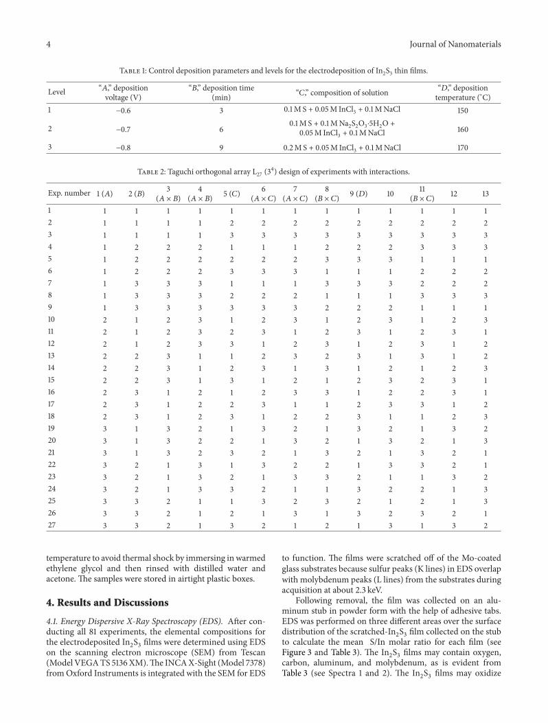
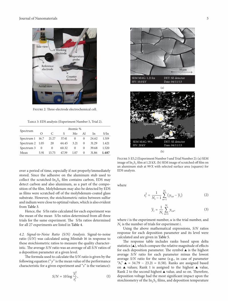
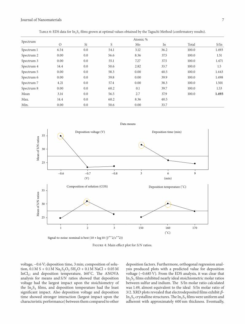
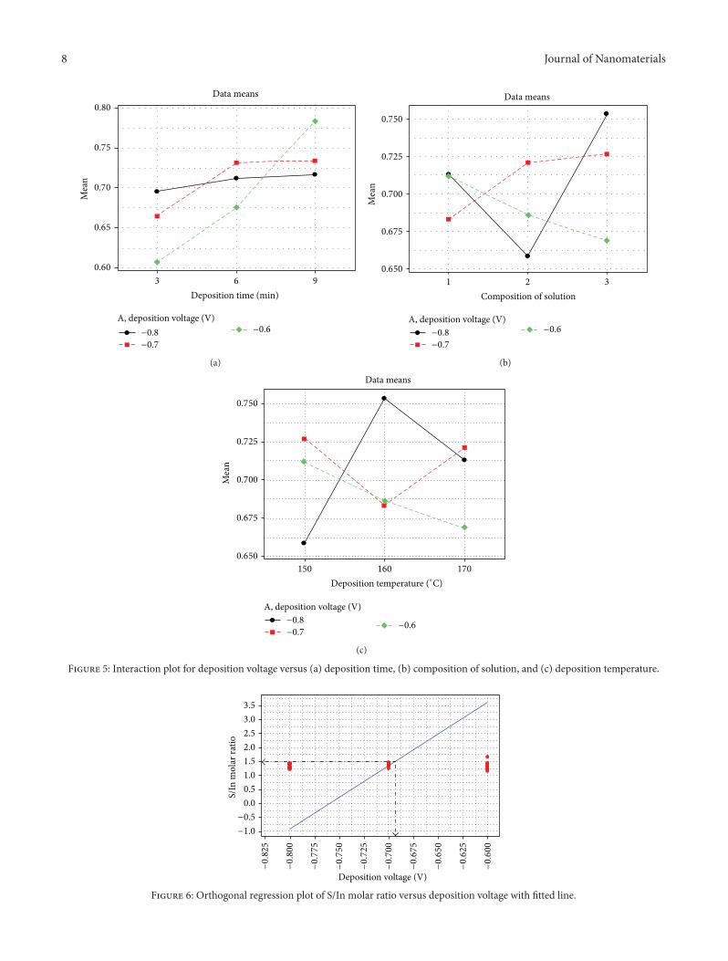
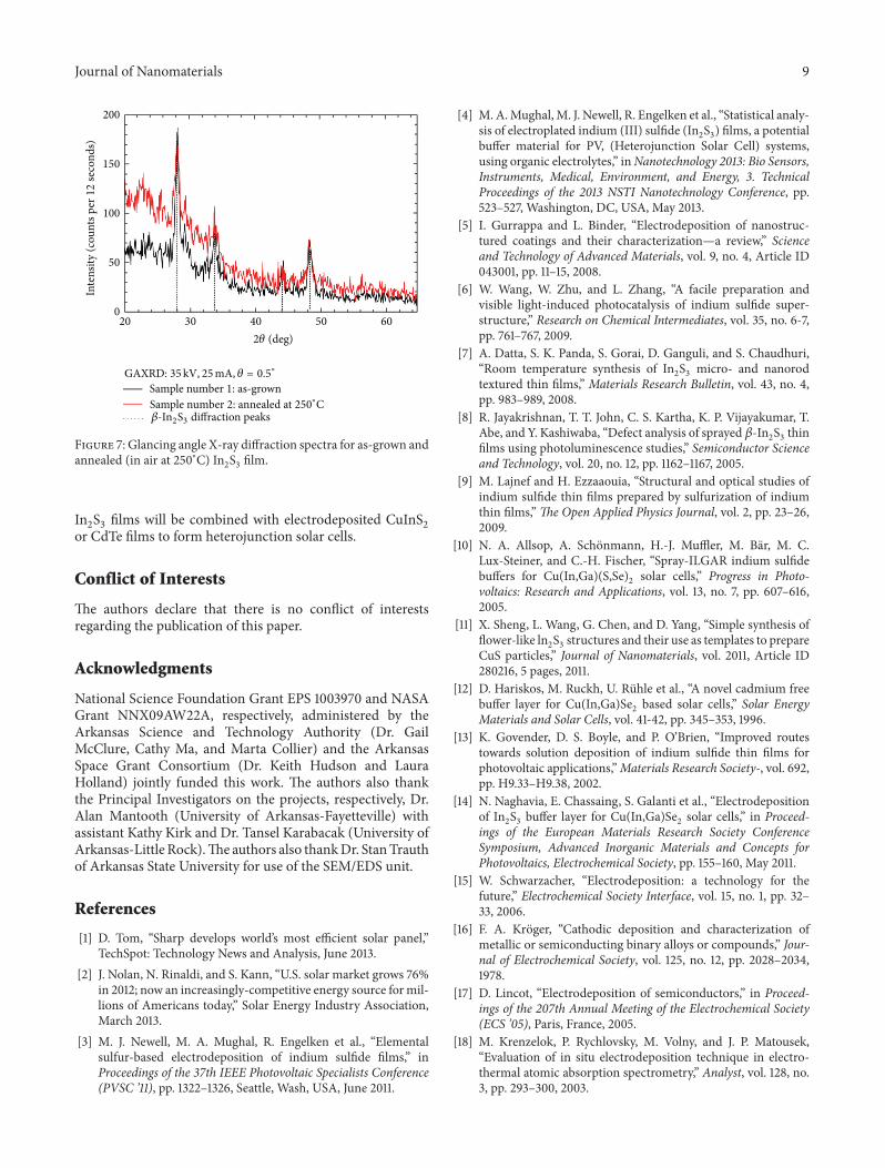
![Electrodeposition of Zn-Mn alloys from recycling battery leach … · 2014. 5. 20. · recovery by electrodeposition [1–4] is currently being studied in our laboratory [5]. Electrodeposition](https://img.pdfslide.us/doc/110x75/6112e3e4b1654c15ca54266d/electrodeposition-of-zn-mn-alloys-from-recycling-battery-leach-2014-5-20-recovery.jpg)