Embed Size (px)
Citation preview
A PRACTICAL TRAINING SEMINAR
onELECTRONICS CIRCUITS DESIGN & COMPONENTS
Pursued at
“OMEGA ELECTRONIC”
Presented by:Jitendra Kumar sirohiya(ECE 4th year)
Submitted to:Mr. Manish Yadav(Lecturer & Seminar Coordinator) (ECE Department)
Contents:
• Company Profile• Products• International Presence• Various Department in Company• Training Program• PCB Designing & fabrication Process• SMT• Introduction of Robotics
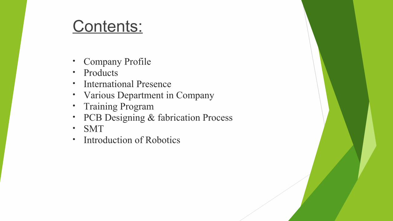
Company Profile:
Mr Y. P. Agarwal, an eminent & qualified Electronic professional, founded OMEGA ELECTRONICS.
It is an ISO certified Company 9001:2000, situated in Malviya Nagar RIICO Industrial Area, Jaipur, (Rajasthan)
It is now a leading manufacturer and exporter of Educational Training Scientific Equipment and Lab Practical Equipment.
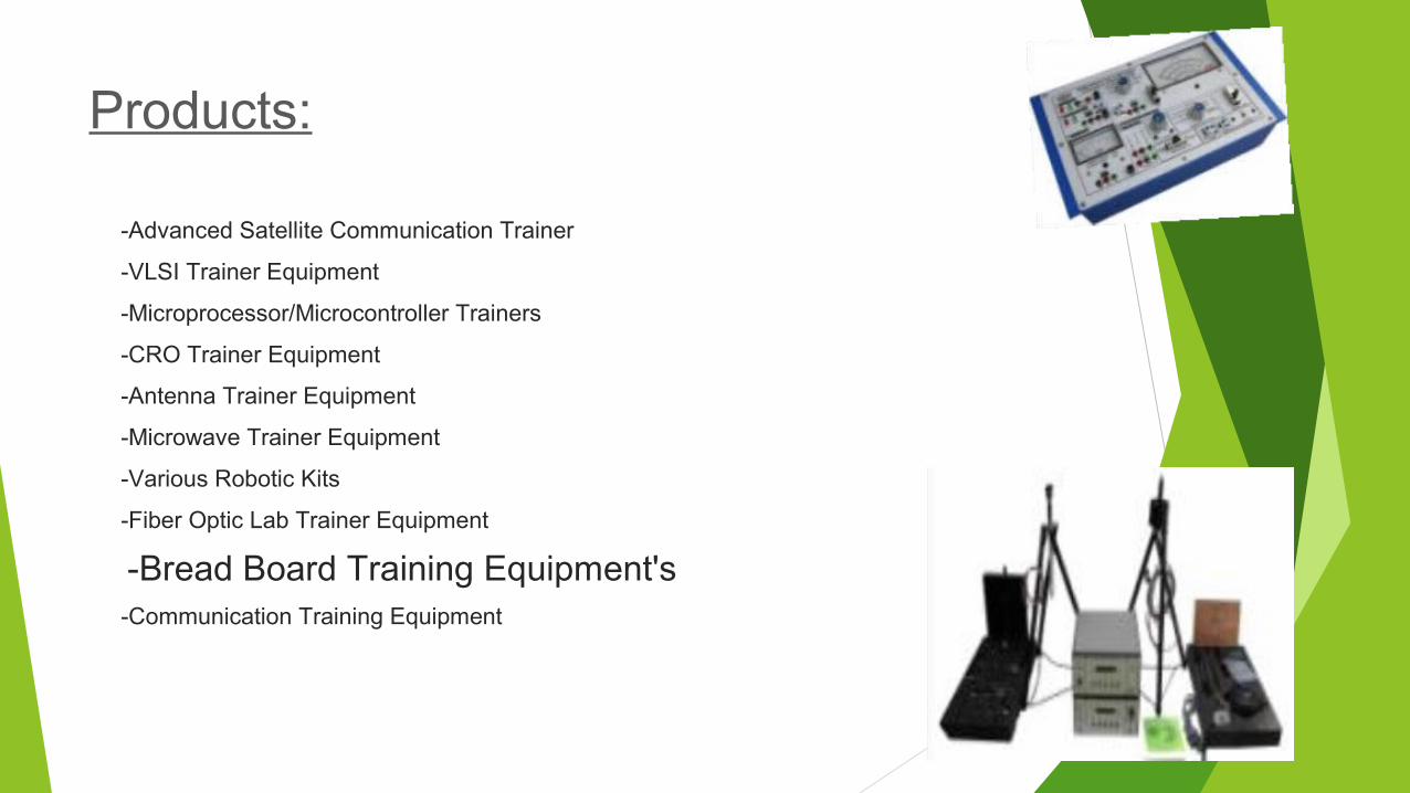
Products:
-Advanced Satellite Communication Trainer
-VLSI Trainer Equipment
-Microprocessor/Microcontroller Trainers
-CRO Trainer Equipment
-Antenna Trainer Equipment
-Microwave Trainer Equipment
-Various Robotic Kits
-Fiber Optic Lab Trainer Equipment
-Bread Board Training Equipment's -Communication Training Equipment

International Presences:
Industrial Visit
An Industrial visit gives awareness about how an industry actually works.
Omega has basically the following sections:
1) Research & Development
2) Equipment Testing
3) Soldering and Desoldering
4) Winding section
5) Paint section
1)Basic Electronics:
The theory of basic electronic device includes introduction of
1) Electronic devices,
2) Components,
3) Circuits,
4) Working,
5) Characteristics,
6) Assembling
7) Applications
8)Advancements and future aspects
2)PCB Designing and fabrication Process:
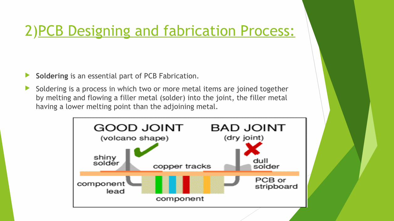
Soldering is an essential part of PCB Fabrication.
Soldering is a process in which two or more metal items are joined together by melting and flowing a filler metal (solder) into the joint, the filler metal having a lower melting point than the adjoining metal.
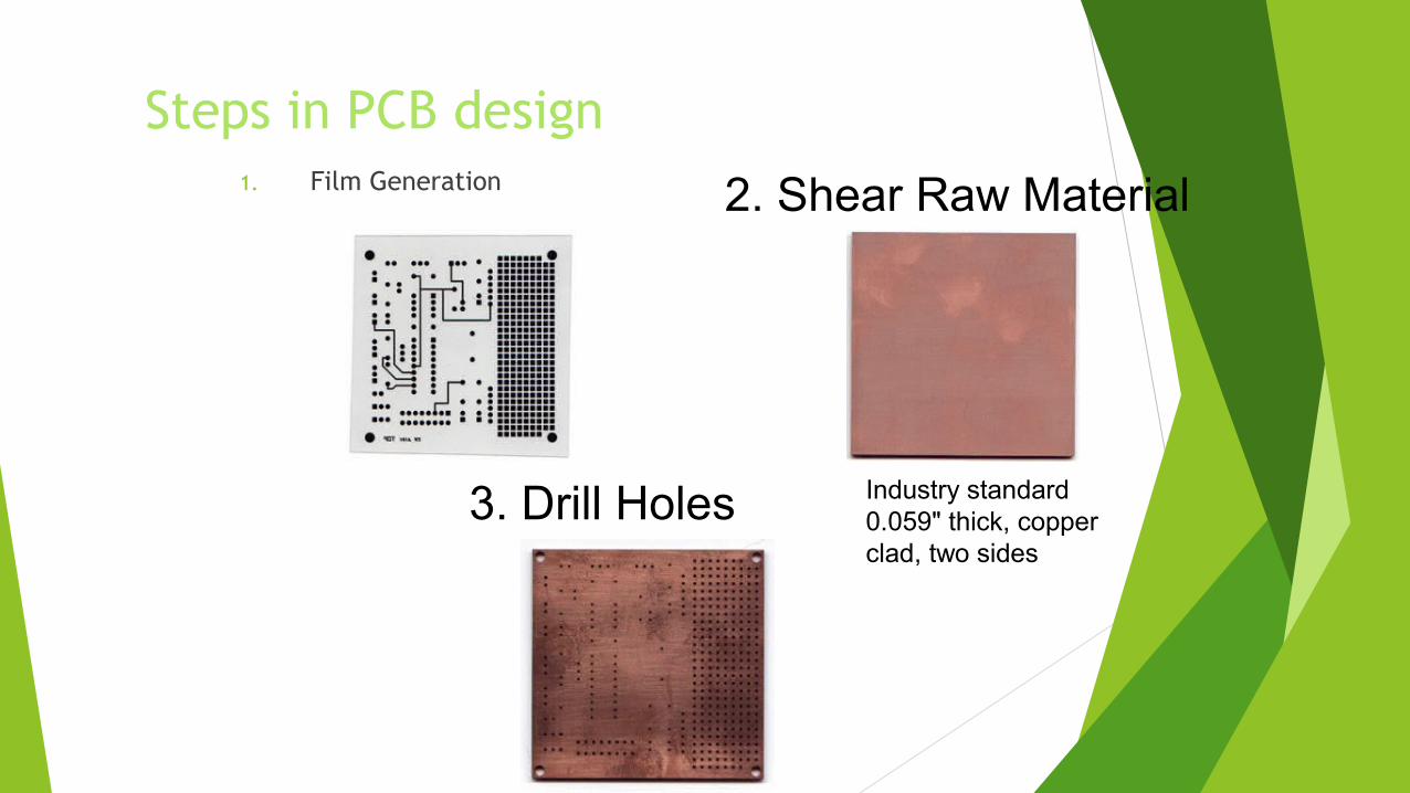
Steps in PCB design1. Film Generation 2. Shear Raw Material
3. Drill Holes Industry standard 0.059" thick, copper clad, two sides
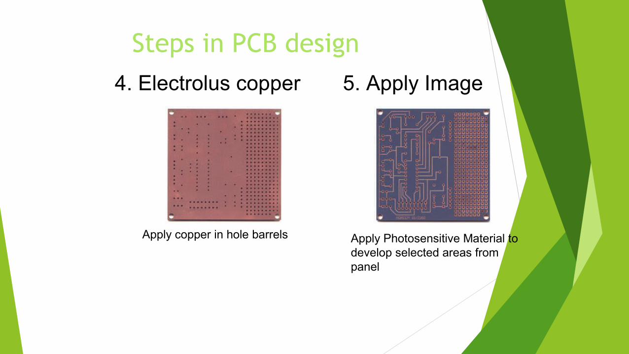
Steps in PCB design
4. Electrolus copper
Apply copper in hole barrels
5. Apply Image
Apply Photosensitive Material to develop selected areas from panel
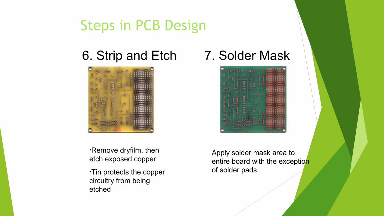
Steps in PCB Design
6. Strip and Etch
•Remove dryfilm, then etch exposed copper
•Tin protects the copper circuitry from being etched
7. Solder Mask
Apply solder mask area to entire board with the exception of solder pads
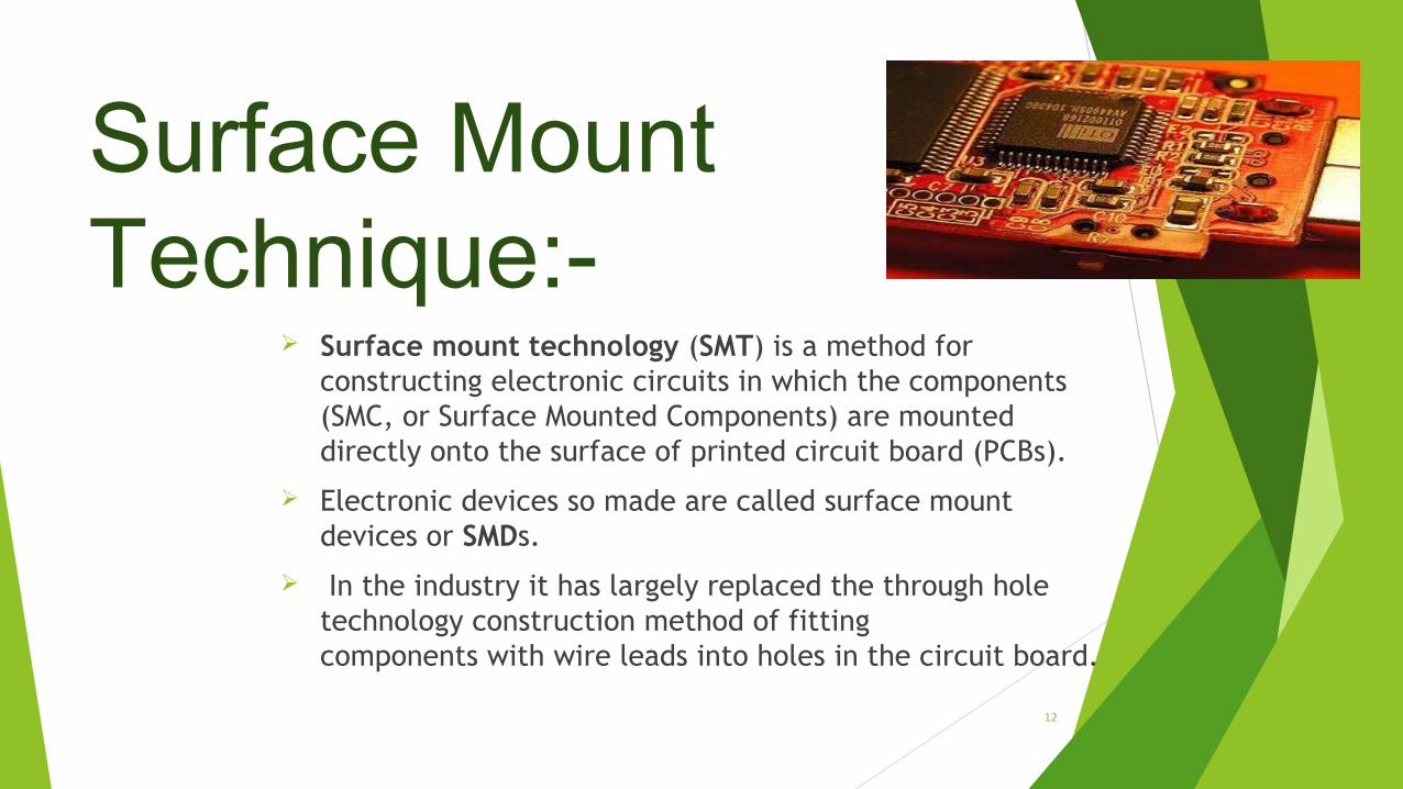
Surface Mount Technique:-
Surface mount technology (SMT) is a method for constructing electronic circuits in which the components (SMC, or Surface Mounted Components) are mounted directly onto the surface of printed circuit board (PCBs).
Electronic devices so made are called surface mount devices or SMDs.
In the industry it has largely replaced the through hole technology construction method of fitting components with wire leads into holes in the circuit board.
12
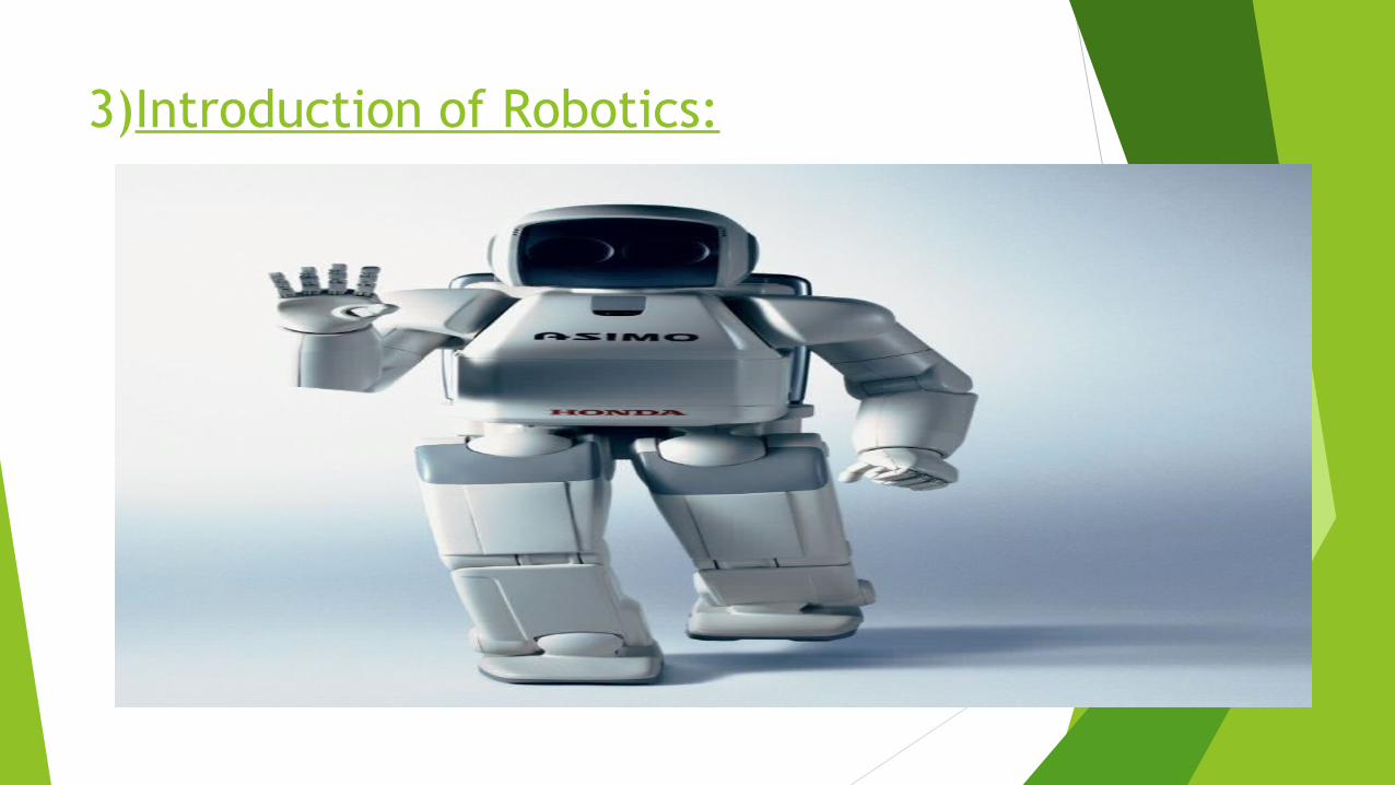
3)Introduction of Robotics:
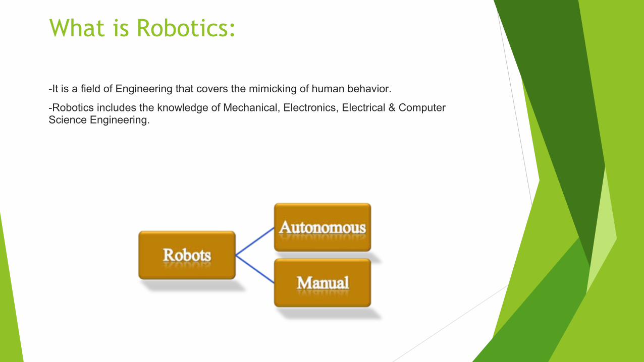
What is Robotics:
• -It is a field of Engineering that covers the mimicking of human behavior.
• -Robotics includes the knowledge of Mechanical, Electronics, Electrical & Computer Science Engineering.
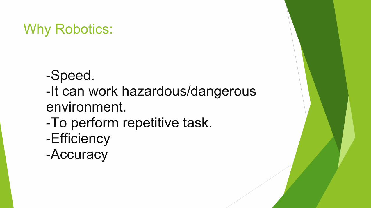
Why Robotics:
• -Speed.• -It can work hazardous/dangerous
environment.• -To perform repetitive task.• -Efficiency• -Accuracy
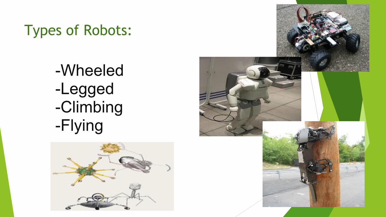
Types of Robots:
• -Wheeled• -Legged• -Climbing• -Flying
Power Supply:
• -Suitable power supply is needed to run the motors and associated circuitry
• -Typical power requirement ranges from 3V to 24V DC• 220V AC supply must be modified to suit the needs of our
machine• -Batteries can also be used to run robots• -Robots are driven by different motors :-
oDC MotorsoStepper Motors oServo Motors
REFERENCE
1.http://www.omegaelectronics.net/profile.asp2.http://electronics.howstuffworks.com/robot.htm3.http://engineering-ed.org/Robotics/documents4.http://html.alldatasheet.com/html

Queries???