Embed Size (px)
Citation preview

LOW POWER HIGH SPEED VEDIC MULTIPLIER USING REVERSIBLE LOGIC GATES: A REVIEW
1M.Anitha 2A.Rajani 3N.Pushpalatha M.Tech (DECS) Student, Assistant professor, Assistant professor
Department of ECE, AITS Annamacharya Institute of Technology and Sciences, Tirupati, India-517520
[email protected] [email protected]
Abstract-- Multipliers design is difficulty and very important in DSP (Digital Signal Processing) systems. It requires more hardware resources and processing time. Multipliers can perform multiplication and addition operations. Real-time signal processing requires high speed and high throughput. Vedic mathematics is one of the algorithms, it having different sutras to perform multiplication in easy way. Urdhva Tiryagbhyam Vedic multiplier is one multiplier that consumes low power, high speed by using reversible logic, which is always a key to achieve a high performance digital signal processing system. In this paper we have to increase the performance of the previous design. Total reversible logic implementation cost is reduced by using proposed method. Multipliers are very important in FFT (Fast Fourier Transforms), Nano Technology, Embedded Systems. By using reversible logic number of garbage outputs, constant inputs, quantum computing is reduced. In order to achieve low power designs Quantum computing and reversible circuits are used. Urdhva Tiryagbhyam Vedic multiplier implementation using reversible logic can be done by Xilinx software using Verilog HDL language. Keywords:- Reversible Logic, Urdhva Tiryagbhyam, TRLIC (Total Reversible Logic Implementation Cost).
I.INTRODUCTION The Sanskrit word Veda is derived from the
root Vid, meaning to know without limit. Vedic mathematics is one of most ancient method to perform mathematical calculations in simple way. It can perform large arithmetic operations to simple mind calculations. The Vedic mathematics having 16 different sutras introduced by Jagadguru swami Sri Bhakti Krishna Tirtha Maharaja, from that Urdhva Tiryagbhyam Vedic multiplier is one type of multiplier which performs crosswise and vertical operations between the two numbers. This Sutra was traditionally used in ancient India for the multiplication of two decimal numbers in relatively less time and useful in digital hardware.
With the advancement in the VLSI Technology, there is an ever increasing demand for the multiplication. Multiplication in DSP is omnipresent in almost every engineering discipline.
In DSP Faster additions and multiplication operations are very important and Multiplication is the most basic and frequently used operations in a CPU (Central Processing Unit). Multiplication is an operation performs multiplication between two binary numbers. Multiplication operations are also important for other complex operations such as convolution, Discrete Fourier Transform (DFT), Fast Fourier Transforms (FFT), etc. DSP engineers are awaited for new method and hardware implementation for the multiplication. For the multiplication DSP engineer has to concentrate on power dissipation and speed. There is a relation between power and speed. The reversible logic computation which takes zero power dissipation. So reversible logic delay is reduced .The reversible Urdhva Tiryagbhyam multiplier has been proposed. The paper is organized as follows: The section II gives the information about reversible logic along with the conventional combinational logic. Section III explains the Urdhva Tiryagbhyam Vedic multiplier algorithm. The section IV describes the Urdhva Tiryagbhyam multiplier using conventional logic. Section V compares the proposed design and draws a conclusion claiming the versatility of reversible Urdhva Tiryagbhyam multiplier.
II. REVERSIBLE LOGIC A. REVERSIBLE LOGIC CIRCUITS
Irreversible circuits (conventional logic
circuits) loosing one bit of information and generates heat by the second law of thermo dynamics. The irreversible logic information dissipates (KTln2) joules of heat energy, where K is Boltzmann's constant and T is the absolute temperature. The reversible logic circuits do not dissipate energy as much as irreversible circuits. The irreversible circuits mapping between input and output is many- to-one (number of inputs=single output).Thus, energy dissipation and the number of bits lost during computation are in direct prapotion. Threshold
INTERNATIONAL CONFERENCE ON CIVIL AND MECHANICAL ENGINEERING, ICCME-2014
INTERNATIONAL ASSOCIATION OF ENGINEERING & TECHNOLOGY FOR SKILL DEVELOPMENT www.iaetsd.in28
ISBN:378-26-138420-0234

voltage and power supply applied for the circuit at that time energy consumption is reduced. In 1973, Bennett, proved that in order to avoid kTln2 joules of energy dissipation for a circuit it must be built from reversible circuits.
In Reversible logic circuits the mapping between input and output is one-to-one mapping (number of inputs=number of outputs). In reversible circuits the input data can uniquely recovered from output data .By using of this technique there is no information lost. In order to achieve low power designs Quantum computing and reversible circuits are used.
B. REVERSIBLE LOGIC GATES:
The reversible logic gates are n-input and n-output logic gates. Reversible logic is similar to the convention logic but reversible logic circuits are constructing by reversible logic gates. We have different reversible logic gates are present for the Urdhva Tiryagbhyam Vedic multiplier. NOT GATE: 1X1 NOT Gate performs complement output of present input as shown in fig(1) and gives zero quantum cost.
Fig(1): Reversible NOT gate
FEYNMAN GATE: 2X2 Feynman Gate mainly used for fan-out purposes. It performs complementing and XOR operations are shown in fig(2) . It is also called as CNOT gate. The quantum cost of Feynman gate is one.
Fig(2) :Reversible Feynman gate
PERES GATE: 3X3 Peres gate performs AND, XOR, complementing operations are shown in fig (3). The quantum cost of Peres gate is four.
Fig(3):Reversible Peres gate
NFT GATE: 3X3 NFT gate performs AND, XOR, complementing operation and its quantum implementation is as shown in the fig(4). The quantum cost of NFT gate is five.
Fig(4):Reversible NFT gate HNG GATE: 4X4 HNG GATE Performs full adder operation as shown in fig(5) and provide minimum quantum cost. The quantum cost is six.
Fig(5):Reversible HNG gate BVPPG GATE: 5X5 BVPPG Gate performs AND, XOR, complementing operation and its quantum implementation is as shown in the fig(6). The quantum cost of BVPPG gate is ten.
Fig(6):Reversible BVPPG gate
Important parameters of reversible logic: The most important parameters of the reversible logic 1. Minimized Constant inputs (CI): By using reversible logic the number of inputs that are to be maintained constant at either 0 or 1 in order to synthesize the given logical function. 2. Minimize the garbage: This garbage referred as number of outputs which are not used in the synthesis of a required function are very essential, without reversibility we can’t achieved. 3. Minimize the width of the circuit: In reversible logic one output given one time as the input of
INTERNATIONAL CONFERENCE ON CIVIL AND MECHANICAL ENGINEERING, ICCME-2014
INTERNATIONAL ASSOCIATION OF ENGINEERING & TECHNOLOGY FOR SKILL DEVELOPMENT www.iaetsd.in29
ISBN:378-26-138420-0235
another gate .so the width of the circuit is reduced by number of additional inputs. 4. Minimize the total number of gates: Based on number of gates usage the delay of the circuit is reduced. Here we are using less number of gates for circuit implementation. 5. Quantum cost (QC): Quantum cost depends on the cost of the circuit in terms of the cost of a primitive gate. It is calculated knowing the number of primitive reversible logic gates (1X1 or 2X2) required to realize the circuit. 6. Total Reversible Logic Implementation Cost (TRLIC): In a reversible logic circuit TRLIC calculated as number of garbage outputs, quantum cost, constant inputs and number of Reversible logic gates .
TRLIC=∑ (NG+CI+GO+QC)…. (1)
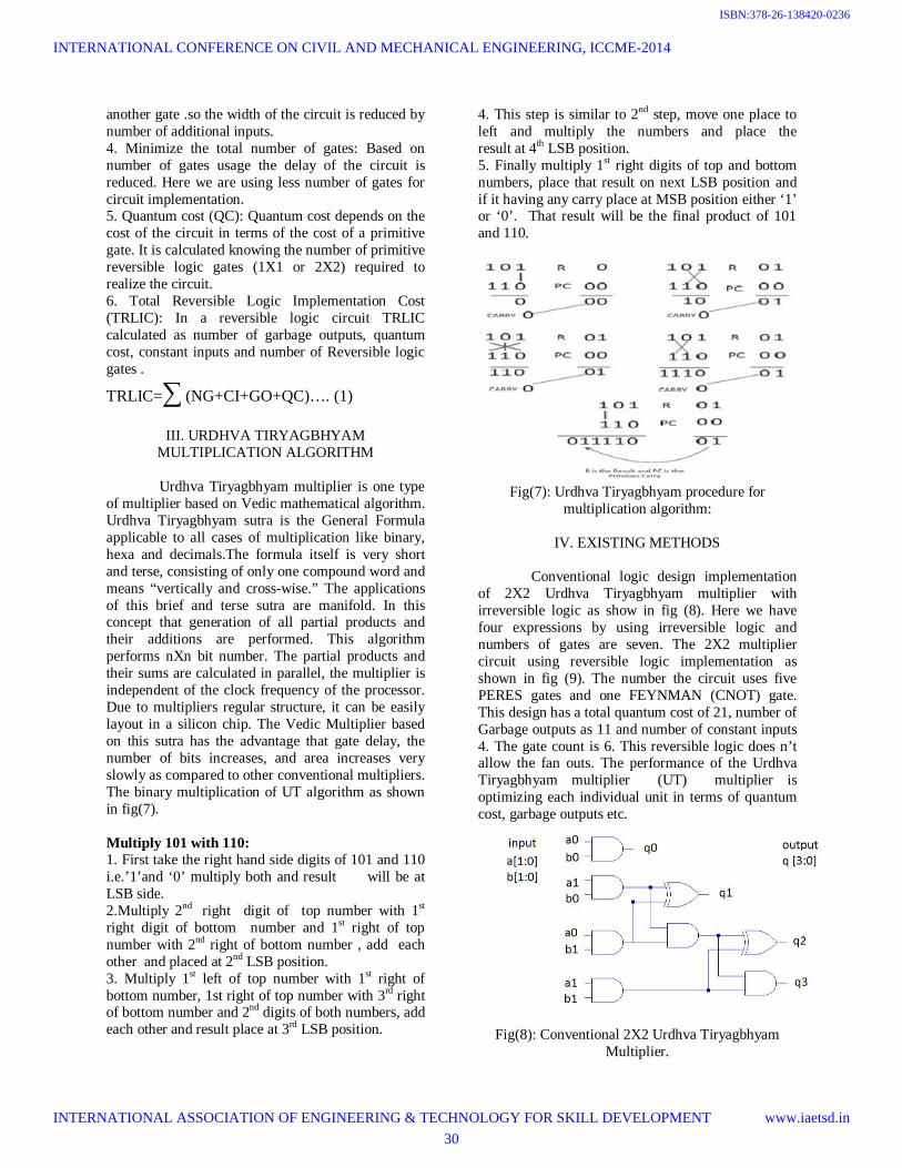
III. URDHVA TIRYAGBHYAM MULTIPLICATION ALGORITHM
Urdhva Tiryagbhyam multiplier is one type
of multiplier based on Vedic mathematical algorithm. Urdhva Tiryagbhyam sutra is the General Formula applicable to all cases of multiplication like binary, hexa and decimals.The formula itself is very short and terse, consisting of only one compound word and means “vertically and cross-wise.” The applications of this brief and terse sutra are manifold. In this concept that generation of all partial products and their additions are performed. This algorithm performs nXn bit number. The partial products and their sums are calculated in parallel, the multiplier is independent of the clock frequency of the processor. Due to multipliers regular structure, it can be easily layout in a silicon chip. The Vedic Multiplier based on this sutra has the advantage that gate delay, the number of bits increases, and area increases very slowly as compared to other conventional multipliers. The binary multiplication of UT algorithm as shown in fig(7). Multiply 101 with 110: 1. First take the right hand side digits of 101 and 110 i.e.’1’and ‘0’ multiply both and result will be at LSB side. 2.Multiply 2nd right digit of top number with 1st right digit of bottom number and 1st right of top number with 2nd right of bottom number , add each other and placed at 2nd LSB position. 3. Multiply 1st left of top number with 1st right of bottom number, 1st right of top number with 3rd right of bottom number and 2nd digits of both numbers, add each other and result place at 3rd LSB position.
4. This step is similar to 2nd step, move one place to left and multiply the numbers and place the result at 4th LSB position. 5. Finally multiply 1st right digits of top and bottom numbers, place that result on next LSB position and if it having any carry place at MSB position either ‘1’ or ‘0’. That result will be the final product of 101 and 110.
Fig(7): Urdhva Tiryagbhyam procedure for
multiplication algorithm:
IV. EXISTING METHODS Conventional logic design implementation
of 2X2 Urdhva Tiryagbhyam multiplier with irreversible logic as show in fig (8). Here we have four expressions by using irreversible logic and numbers of gates are seven. The 2X2 multiplier circuit using reversible logic implementation as shown in fig (9). The number the circuit uses five PERES gates and one FEYNMAN (CNOT) gate. This design has a total quantum cost of 21, number of Garbage outputs as 11 and number of constant inputs 4. The gate count is 6. This reversible logic does n’t allow the fan outs. The performance of the Urdhva Tiryagbhyam multiplier (UT) multiplier is optimizing each individual unit in terms of quantum cost, garbage outputs etc.
Fig(8): Conventional 2X2 Urdhva Tiryagbhyam Multiplier.
INTERNATIONAL CONFERENCE ON CIVIL AND MECHANICAL ENGINEERING, ICCME-2014
INTERNATIONAL ASSOCIATION OF ENGINEERING & TECHNOLOGY FOR SKILL DEVELOPMENT www.iaetsd.in30
ISBN:378-26-138420-0236
A.2X2 URDHVA TIRYAKBHYAM MULTIPLIER:
The design expressions of multiplier can be logically modified, so as to optimize the design. This optimized design makes use of on BVPPG, three Peres gates and a single FEYNMAN gate. The design implementation can be optimized using reversible logic, so the constraints are fan-outs. Other being loops not permitted. This means that the reversible logic circuit with multiple numbers of same inputs is not allowed. In this optimized design One way out is to use a separate fan out generator or to build a circuit that inherently takes care of fan outs using the reversible logic gates used. This optimized design has a quantum cost of 23, number of garbage outputs as 5, number of gates 5 and the number of constant inputs is 5.
Fig(9): Design of 2X2 UT multiplier using reversible logic
Fig(10): Improved Design of 2X2 UT multiplier using reversible logic -1
The next optimized design also considers the
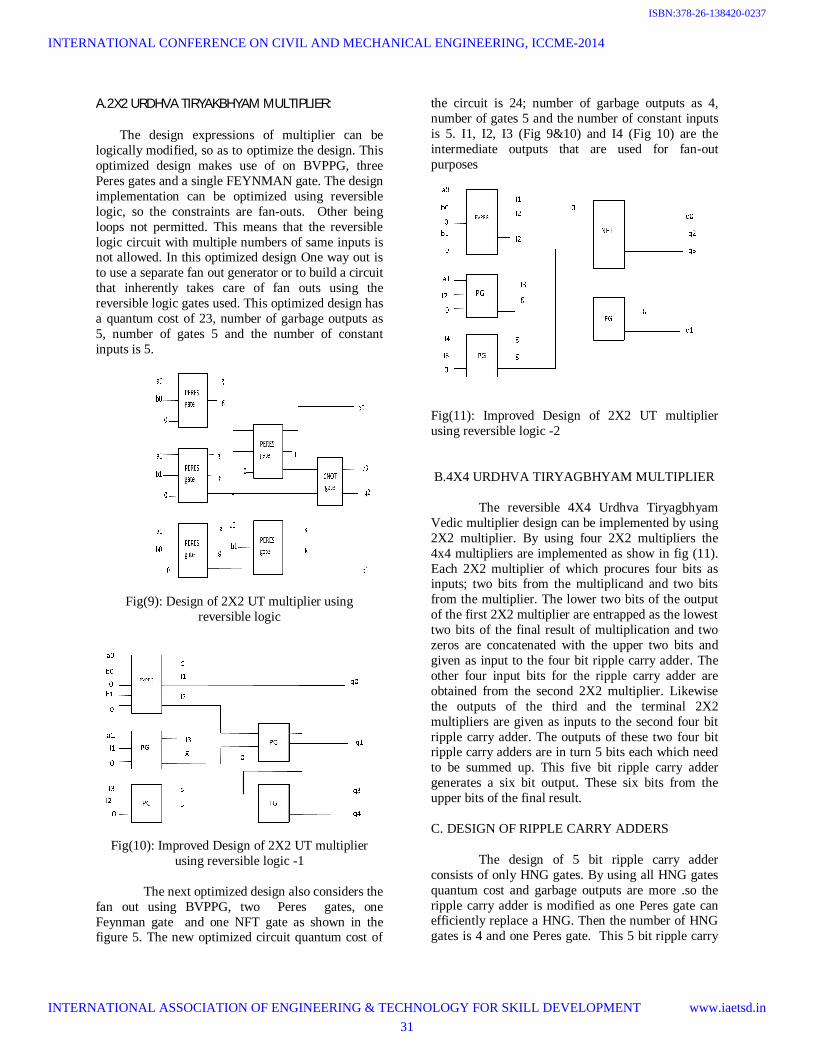
fan out using BVPPG, two Peres gates, one Feynman gate and one NFT gate as shown in the figure 5. The new optimized circuit quantum cost of
the circuit is 24; number of garbage outputs as 4, number of gates 5 and the number of constant inputs is 5. I1, I2, I3 (Fig 9&10) and I4 (Fig 10) are the intermediate outputs that are used for fan-out purposes
Fig(11): Improved Design of 2X2 UT multiplier using reversible logic -2 B.4X4 URDHVA TIRYAGBHYAM MULTIPLIER
The reversible 4X4 Urdhva Tiryagbhyam Vedic multiplier design can be implemented by using 2X2 multiplier. By using four 2X2 multipliers the 4x4 multipliers are implemented as show in fig (11). Each 2X2 multiplier of which procures four bits as inputs; two bits from the multiplicand and two bits from the multiplier. The lower two bits of the output of the first 2X2 multiplier are entrapped as the lowest two bits of the final result of multiplication and two zeros are concatenated with the upper two bits and given as input to the four bit ripple carry adder. The other four input bits for the ripple carry adder are obtained from the second 2X2 multiplier. Likewise the outputs of the third and the terminal 2X2 multipliers are given as inputs to the second four bit ripple carry adder. The outputs of these two four bit ripple carry adders are in turn 5 bits each which need to be summed up. This five bit ripple carry adder generates a six bit output. These six bits from the upper bits of the final result. C. DESIGN OF RIPPLE CARRY ADDERS
The design of 5 bit ripple carry adder consists of only HNG gates. By using all HNG gates quantum cost and garbage outputs are more .so the ripple carry adder is modified as one Peres gate can efficiently replace a HNG. Then the number of HNG gates is 4 and one Peres gate. This 5 bit ripple carry
INTERNATIONAL CONFERENCE ON CIVIL AND MECHANICAL ENGINEERING, ICCME-2014
INTERNATIONAL ASSOCIATION OF ENGINEERING & TECHNOLOGY FOR SKILL DEVELOPMENT www.iaetsd.in31
ISBN:378-26-138420-0237

adder is used in the second stage of the 4X4 Urdhva Tiryagbhyam Multiplier. Since for any ripple carry adder the input carry for the first full adder is zero, this implicitly means the first adder is a half adder. Thus a Peres gate HNG. This cut down the quantum cost by two for any ripple carry adder and the garbage output by one. The Constant inputs and the gate count remain constant. The 4X4 UT multiplier structure is as shown in figure (12).
Fig(11):5-Bit ipple carry adder
Fig(12):4-Bit ripple carry adder
V. RESULTS AND COMPARISONS
The design of the Urdhva Tiryagbhyam
multiplier reversible 2x2 and 4x4 multipliers is logically verified using XILINX 9.2i and MODELSIM. The simulation results are as shown in figures 10 and 11 respectively. The following are the important design constraints for any reversible logic circuits.
1. Quantum cost of Reversible logic circuit should be minimum. 2. Number of garbage outputs of Reversible logic circuit should be minimum. 3. Number of constant inputs of Reversible logic circuit should be minimum.
4. Number of reversible gates of Reversible logic circuit should be minimum. Total reversible logic implementation cost calculated as summing of all constraints and based on above constraints the total reversible logic implementation cost is reduced. The 4X4 Vedic multiplier using reversible logic compared with another multipliers as shown in table 1. The 4x4 multipliers are take care of fan outs also. So the quantum cost of 2x2 UT multipliers quantum cost is increased compare to previous designs.
Fig(14):Block diagram of 4X4 UT multiplier
Fig(15):Output waveform for 2X2 Multiplier using Conventional logic .
INTERNATIONAL CONFERENCE ON CIVIL AND MECHANICAL ENGINEERING, ICCME-2014
INTERNATIONAL ASSOCIATION OF ENGINEERING & TECHNOLOGY FOR SKILL DEVELOPMENT www.iaetsd.in32
ISBN:378-26-138420-0238

CONCLUSIONS The main aim of UT algorithm is mainly to
design a low power and high speed multipliers using reversible logic gates. This is the optimized design as compared to conventional multiplier. The efficiency of reversible logic circuit is realized in terms of number of gates, quantum cost, constant inputs, and garbage outputs. If these parameters are less the
circuit is efficient. By reducing these parameters the TRLIC is reduced and also lower TRLIC implicitly means lower the quantum cost, hence lower the delay and vice versa. Besides combining the design criterion that fan-out must be generated with the reversible logic. The further optimization of the circuit in terms of high speed and low power as future work.
Table (1): Comparisons of Existing, implemented methods of 2x2 Multiplier and 4x4 Multiplier ACKNOWLEDGMENTS We would like to thank our Parents and Teachers who have been constantly supporting all our works.
REFERENCES [1] Swami Bharati Krsna Tirtha, Vedic Mathematics. Delhi: Motilal Banarsidass publishers 1965. [2]VedicMathematics: http://www.hinduism.co.za/vedic.html. [3] R. Landauer,"Irreversibility and Heat Generation in the Computational Process", IBM Journal of Research and Development, 5, pp.183-191, 1961. [4] C.H. Bennett, "Logical reversibility of Computation", IBM J. Research and Development, pp.525-532, November
[8] E. Fredkin and T. Toffoli,"Conservative Logic", Int'l 1 Theoretical Physics Vo121, pp.219-253, 1982. [9]. Reversible logic gates http://www.reversible logic gates.com [10].http://multipliers using reversible logic and implementation. [11] Rakshith Saligram and Rakshith T.R. "Novel Code Converter Employing Reversible Logic", International Journal of Computer Applications (IJCA),August2012. [12] M. Haghparast et al. , "Design of a Novel Reversible Multiplier Circuit using HNG Gate in Nanotechnology," in World Applied Science Journal, Vol. 3, No. 6, pp. 974-978, 2008.
[5] Thapliyal, H., M.B. Srinivas and H.R. Arabnia, 2005, A Reversible Version of 4x4 Bit Array Multiplier with Minimum Gates and Garbage Outputs, Int. Conf. Embedded System, Applications (ESA'05), Las Vegas, USA, pp: 106 114. [6] M. S. Islam et al. , "Realization of Reversible Multiplier Circuit," in Information Tech. 1, Vol. 8, No. 2, pp. 117-121, 2005.
[7] H. R. Bhagyalakshmi, M. K. Venkatesha, “An Improved Design of a Multiplier using Reversible Logic Gates,” IJEST, Vol. 2, No. 8, 2010.
[13] G Ganesh Kumarand V Charishma, Design of high speed vedic multiplier using vedic mathematics techniques, ltn'l J. of Scientific and Research Publications, Vol. 2 Issue 3 March 2012
Multiplier design Number of gates
Constant inputs Garbage outputs
Quantum cost TRLIC
4X4 UT multiplier using reversible logic
34
2
Reduced Reduced
reduced
2X2 UT multiplier using Conventional logic
11
4
11
21
47
Improved Design-1 of 2X2 UT multiplier
5
5
5
23
38
Improved Design-2 of 2X2 UT multiplier
5
5
4
24
38
INTERNATIONAL CONFERENCE ON CIVIL AND MECHANICAL ENGINEERING, ICCME-2014
INTERNATIONAL ASSOCIATION OF ENGINEERING & TECHNOLOGY FOR SKILL DEVELOPMENT www.iaetsd.in33
ISBN:378-26-138420-0239