Embed Size (px)
Citation preview
COURSE SUBJECT
ELECTROMAGNETIC SHIELDING
OFFERED By
Prof.Dr. Mustfa Merdan
Submitted by
Khalid Saeed Al-Badri
1
T.C
SÜLEMAN DEMİREL UNIVERSITY
FEN BİLİMLERİ ENSTİTÜSÜ
Mühendislik fakültesi
ELEKTRONİK VE HABERLEŞME MÜHENDİSLİĞİ
COURSE SUBJECT
ELECTROMAGNETIC
SHIELDING
COURSE OFFERED By
Prof. Dr. Mustafa MERDAN
ELECTROMAGNETIC SHIELDING SINGLE
AND MULTIPLE SHIELDING LAYERS
USING SHIELDING EFFECTIVENESS
DEPENDING ON IMPEDANCE METHOD
Submitted by MSc. Student
Badri -Khalid Saeed Lateef Al
Student No. 1330145002
2
ELECTROMAGNETIC SHIELDING SINGLE
AND MULTIPLE SHIELDING LAYERS
USING SHIELDING EFFECTIVENESS
DEPENDING ON IMPEDANCE METHOD
Submitted by MSc. Student
Khalid S. Al-Badri

3
I
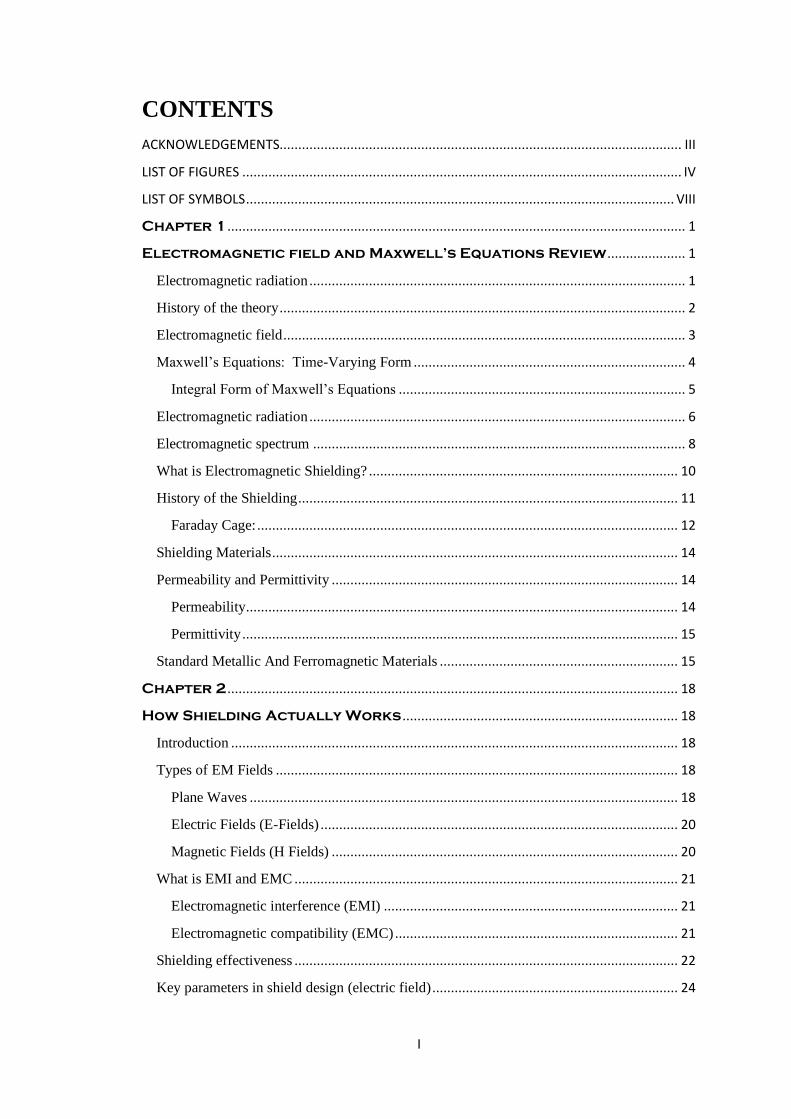
CONTENTS
ACKNOWLEDGEMENTS............................................................................................................ III
LIST OF FIGURES ...................................................................................................................... IV
LIST OF SYMBOLS ................................................................................................................... VIII
Chapter 1 ........................................................................................................................... 1
Electromagnetic field and Maxwell’s Equations Review ..................... 1
Electromagnetic radiation ..................................................................................................... 1
History of the theory ............................................................................................................. 2
Electromagnetic field ............................................................................................................ 3
Maxwell’s Equations: Time-Varying Form ......................................................................... 4
Integral Form of Maxwell’s Equations ............................................................................. 5
Electromagnetic radiation ..................................................................................................... 6
Electromagnetic spectrum .................................................................................................... 8
What is Electromagnetic Shielding? ................................................................................... 10
History of the Shielding ...................................................................................................... 11
Faraday Cage: ................................................................................................................. 12
Shielding Materials ............................................................................................................. 14
Permeability and Permittivity ............................................................................................. 14
Permeability.................................................................................................................... 14
Permittivity ..................................................................................................................... 15
Standard Metallic And Ferromagnetic Materials ................................................................ 15
Chapter 2 ......................................................................................................................... 18
How Shielding Actually Works .......................................................................... 18
Introduction ........................................................................................................................ 18
Types of EM Fields ............................................................................................................ 18
Plane Waves ................................................................................................................... 18
Electric Fields (E-Fields) ................................................................................................ 20
Magnetic Fields (H Fields) ............................................................................................. 20
What is EMI and EMC ....................................................................................................... 21
Electromagnetic interference (EMI) ............................................................................... 21
Electromagnetic compatibility (EMC) ............................................................................ 21
Shielding effectiveness ....................................................................................................... 22
Key parameters in shield design (electric field) .................................................................. 24
II
Skin Depth ...................................................................................................................... 24
Chapter 3 ......................................................................................................................... 28
Effectiveness of Single and Malty Layers Shielding ............................ 28
Introduction ........................................................................................................................ 28
Plane Wave Propagation ..................................................................................................... 28
NEAR FIELDS AND FAR FIELDS .................................................................................. 30
Reflection and Refraction at Plane Interface between Two Media: Oblique Incidence . 34
Single Dielectric Slab ......................................................................................................... 36
Absorption .......................................................................................................................... 37
Internal Reflection .............................................................................................................. 38
Case Study (single Slab) ..................................................................................................... 39
Numerical Example ............................................................................................................ 46
Multilayer Structures .......................................................................................................... 48
Two Dielectric Layer Slabs Structure ............................................................................. 48
More Than Two Dielectric Layer Slabs Structure .......................................................... 50
Absorber Materials ............................................................................................................. 52
Microwave Absorber Materials .......................................................................................... 55
Resonant Absorbers ............................................................................................................ 57
Dallenbach Tuned Layer Absorbers ............................................................................... 58
Salisbury Screens............................................................................................................ 60
Jaumann Layers .............................................................................................................. 61
Graded Dielectric Absorbers: Impedance Matching ........................................................... 63
Pyramidal Absorbers ...................................................................................................... 63
Tapered Loading Absorbers............................................................................................ 65
Matching Layer Absorbers ............................................................................................. 66
Cavity Damping Absorbers ................................................................................................ 67
Anechoic Chambers ............................................................................................................ 69
Absorber Materials Used in Anechoic Chambers ............................................................... 70
Metamaterial Shielding....................................................................................................... 72
Metamaterials Introduction ............................................................................................. 72
Shielding With Metamaterial .......................................................................................... 74
References .............................................................................................................................. 80
III
ACKNOWLEDGEMENTS
I should present my private thanks to Prof. Dr. Mustafa MERDAN, for his excellent help, guidance, and encouragement me with an excellent atmosphere. And I should present many thanks to my family father, mother, and my brothers. Also I present greet thanks to my wife and child
Khalid SAEED AL-BADRI Isparta, 2015
IV
LIST OF FIGURES FIGURE 1. THE MAGNETISM IS ULTIMATELY CAUSED BY MOVING ELECTRIC CHARGES OR
CURRENT, WHEN HE OBSERVED A MAGNETIC COMPASS NEEDLE TO REACT TO A
CURRENT FLOWING THROUGH A WIRE PLACED NEAR IT ...................................... 1
FIGURE 2. JAMES CLERK MAXWELL'S 1873 ......................................................... 2
FIGURE 3. AN ELECTRIC CURRENT IN A WIRE CREATES A CIRCULAR MAGNETIC FIELD
AROUND THE WIRE, ITS DIRECTION (CLOCKWISE OR COUNTER-CLOCKWISE)
DEPENDING ON THAT OF THE CURRENT .......................................................... 3
FIGURE 4. AN ELECTROMAGNETIC FIELD (ALSO EMF OR EM FIELD) IS A PHYSICAL FIELD
PRODUCED BY ELECTRICALLY CHARGED OBJECTS ............................................... 4
FIGURE 5. THE ELECTROMAGNETIC PLANE WAVE. .................................................. 7
FIGURE 6 ..................................................................................................... 9
FIGURE 7. THE PURPOSE OF THE SHIELD IS TO PROTECT THE INNER DEVICE
FROM IMPINGING ELECTRIC FIELDS AND THUS LESSEN THE EXTENT OF
THE MAGNETIC FIELD. AND PREVENT THE OUTSIDE FROM RADIATION OF
DEVICE. ............................................................................................. 11
FIGURE 8. MICHAEL FARADAY LIVED FROM 1791—1867, AND WAS AN ENGLISH
SCIENTIST. ........................................................................................... 12
FIGURE 9. THE FARADAY CAGE ....................................................................... 13
FIGURE 10. (A) AN DIAGRAM OF A PLAIN WAVE ,E ELECTRIC FIELD H MAGNETIC FIELD .. 19
FIGURE 11. EXAMPLE EXAMINE THE SHIELDING EFFECTIVENESS (10) ....................... 22
FIGURE 12. THE INCIDENT AND THE REFLECTION OF FIELD ..................................... 23
FIGURE 13. PHYSICAL EXPLANATION OF SKIN EFFECT ........................................... 25
FIGURE 14. THIN SHIELD ............................................................................... 26
FIGURE 15. EDDY CURRENTS (ALSO CALLED FOUCAULT CURRENTS) ARE CIRCULAR
ELECTRIC CURRENTS INDUCED WITHIN CONDUCTORS BY A CHANGING MAGNETIC FIELD
IN THE CONDUCTOR, DUE TO FARADAY'S LAW OF INDUCTION. EDDY CURRENTS FLOW
IN CLOSED LOOPS WITHIN CONDUCTORS, IN PLANES PERPENDICULAR TO THE
MAGNETIC FIELD. THEY CAN BE INDUCED WITHIN NEARBY STATIONARY CONDUCTORS
BY A TIME-VARYING MAGNETIC FIELD CREATED BY AN AC ELECTROMAGNET OR
TRANSFORMER, FOR EXAMPLE, OR BY RELATIVE MOTION BETWEEN A MAGNET AND A
NEARBY CONDUCTOR. THE MAGNITUDE OF THE CURRENT IN A GIVEN LOOP IS
PROPORTIONAL TO THE STRENGTH OF THE MAGNETIC FIELD, THE AREA OF THE LOOP,
AND THE RATE OF CHANGE OF FLUX, AND INVERSELY PROPORTIONAL TO THE
RESISTIVITY OF THE MATERIAL. .................................................................. 27
V
FIGURE 16. E PLANE PERPENDICULAR TO THE VECTOR Β IS SEEN FROM ITS SIDE APPEARING
AS A LINE P-W. THE DOT PRODUCT NΒ · R IS THE PROJECTION OF THE RADIAL VECTOR
R ALONG THE NORMAL TO THE PLANE AND WILL HAVE THE CONSTANT VALUE OM FOR
ALL POINTS ON THE PLANE. THE EQUATION Β · R = CONSTANT IS THE CHARACTERISTIC
PROPERTY OF A PLANE PERPENDICULAR TO THE DIRECTION OF PROPAGATION Β. .... 29
FIGURE 17. THE UNIT VECTOR NΒ ALONG Β AND Η IS THE WAVE IMPEDANCE IN THE
PROPAGATION MEDIUM. ......................................................................... 30
FIGURE 18. THE SPACE SURROUNDING A SOURCE OF RADIATION CAN BE DIVIDED INTO
TWO REGIONS, THE NEAR FIELD AND THE FAR FIELD. THE TRANSITION FROM NEAR TO
FAR FIELD OCCURS AT A DISTANCE OF L/2 . (23) ......................................... 31
FIGURE 19. WAVE IMPEDANCE DEPENDS ON THE DISTANCE FROM THE SOURCE. ......... 32
FIGURE 20. TWO MEDIA WITH ELECTRICAL PROPERTIES 1AND 1 IN MEDIUM
1, AND2 AND 2 IN MEDIUM 2. HERE A PLANE WAVE INCIDENT ANGLE
i ON A BOUNDARY BETWEEN THE TWO MEDIA WILL BE PARTIALLY
TRANSMITTED INTO AND PARTIALLY REFLECTED AT THE DIELECTRIC
SURFACE. THE TRANSMITTED WAVE IS REFLECTED INTO THE SECOND
MEDIUM, SO ITS DIRECTION OF PROPAGATION IS DIFFERENT FROM THE
INCIDENCE WAVE. ............................................................................. 34
FIGURE 21. SINGLE DIELECTRIC SLAB, LET L1 BE THE WIDTH OF THE SLAB,
K1 = Ω/C1 THE PROPAGATION WAVENUMBER, AND Λ1 = 2Π/K1 THE
CORRESPONDING WAVELENGTH WITHIN THE SLAB. WE HAVE Λ1 =
Λ0/N1, WHERE Λ0 IS THE FREE-SPACE WAVELENGTH AND N1 THE
REFRACTIVE INDEX OF THE SLAB. WE ASSUME THE INCIDENT FIELD IS
FROM THE LEFT MEDIUM ΗA, AND THUS, IN MEDIUM ΗB THERE IS ONLY A
FORWARD WAVE. .............................................................................. 36
FIGURE 22. PLANE WAVE INCIDENT ON A SHIELDING MATERIAL EINC IS E INCIDENT AND HINC
IS H INCIDENT, EFOR IS E FORWARD AND HFOR
IS H FORWARD, EREV IS E REVERSE AND
HREV IS H REVERSE, ETRAN
IS E TRANSMITTED AND HTRANS IS H TRANSMITTED, Μ
PERMEABILITY OF MATERIAL Ε PERMITTIVITY OF MATERIAL SLAB, Σ CONDUCTIVITY OF
MATERIAL SLAB, Μ0 PERMEABILITY OF FREE SPACE Ε0 PERMITTIVITY OF FREE SPACE, T
THICKNESS OF MATERIAL SLAB. .................................................................. 40
VI
FIGURE 23 FUNCTION OF PLANE WAVE INCIDENT ON A SHIELDING MATERIAL AT INTERFACE
WITH Z=0 THE INTERFACE#2 WITH Z=T, EINC IS E INCIDENT AND HINC
IS H INCIDENT,
EFOR IS E FORWARD AND HFOR
IS H FORWARD, EREV IS E REVERSE AND HREV
IS H
REVERSE, ETRAN IS E TRANSMITTED AND HTRANS
IS H TRANSMITTED, Μ PERMEABILITY OF
MATERIAL Ε PERMITTIVITY OF MATERIAL SLAB, Σ CONDUCTIVITY OF MATERIAL SLAB,
Μ0 PERMEABILITY OF FREE SPACE Ε0 PERMITTIVITY OF FREE SPACE, T THICKNESS OF
MATERIAL SLAB. .................................................................................... 43
FIGURE 24. SINGLE DIELECTRIC SLAB WHERE Ρ,Τ AND Ρ’, Τ’ ARE THE
ELEMENTARY REFLECTION AND TRANSMISSION COEFFICIENTS FROM THE
LEFT AND FROM THE RIGHT OF THE INTERFACE. (13) ........................... 48
FIGURE 25. TWO DIELECTRIC SLABS (13) .......................................................... 49
FIGURE 26. MULTILAYER DIELECTRIC SLAB STRUCTURE. ........................................ 51
FIGURE 27. RESONANT ABSORBERS. DALLENBACH LAYER , SALISBURY
SCREEN , JAUMANN LAYERS (8) ........................................................ 57
FIGURE 28. CALCULATED REFLECTIVITY PROFILES OF A SINGLE LAYER
DALLENBACH ABSORBER AS A FUNCTION OF ABSORBER THICKNESS.
BLUE (1 MM), RED (1.4 MM), BLACK (2 MM), GREEN (3.3MM) AND PINK
(7.6 MM). .......................................................................................... 59
FIGURE 29. 10 GHZ SALISBURY SCREENS MADE USING EEONTEX FABRICS. THE POSITION
AND DEPTH OF THE LOSS PEAK WILL VARY SLIGHTLY DEPENDING ON THE SURFACE
RESISTIVITY AND THICKNESS OF THE FABRIC. EEONTEX CONDUCTIVE FABRIC IS USED IN
SALISBURY SCREEN CONFIGURATIONS IN GROUND PENETRATING RADARS ............. 60
FIGURE 30. AVERAGE OPTIMIZED SHEET RESISTANCES AS A FUNCTION OF INCIDENT ANGLE
FOR A FOUR LAYER JAUMANN ABSORBER OPTIMIZED FOR MAXIMUM BANDWIDTH
BELOW –20 DB. SPACER THICKNESS IS ADJUSTED AT EACH INCIDENT ANGLE
ACCORDING TO EQUATION 19. LOW RESISTANCE SET CORRESPOND TO SHEET
NEAREST THE PEC AND HIGHEST RESISTANCE SET CORRESPONDS TO SHEET NEXT TO
AIR. UNCERTAINTY BARS INDICATE RESISTANCE RANGES THAT PRODUCED THE SAME
BANDWIDTH. SPACER PERMITTIVITY = 1.1. .................................................. 62
FIGURE 31. GRADED DIELECTRIC ABSORBERS BY IMPEDANCE MATCHING.
PYRAMIDAL ABSORBER, TAPED LOADING ABSORBER AND, MATCHING
LAYER ABSORBER .............................................................................. 64
FIGURE 32. THIS CLASS OF ABSORBER HAS BEEN DEVELOPED SPECIFICALLY FOR RADIATED
EMISSION TEST CHAMBERS. IT IS ALSO USEFUL IN OTHER APPLICATIONS SUCH AS
RADIATED SUSCEPTIBILITY. GIVE GOOD REFLECTIVITY PERFORMANCE IN THE CRITICAL
LOW-FREQUENCY RANGE (FROM 30 MHZ UP) OF EMC/EMI TEST CHAMBERS.
VII
HOWEVER, THE ABSORBER STILL PERFORMS MORE THAN ADEQUATELY AT HIGHER
FREQUENCIES UP TO AT LEAST 18 GHZ. ...................................................... 65
FIGURE 33. TRANSFER MATRIX REPRESENTATION FOR A SINGLE LAYER AND A GENERIC
THREE-LAYER STRUCTURE. ....................................................................... 67
FIGURE 34. IN THE ABOVE CLIC ACCELERATING CELL,
\CITEGRUDIEV2009POSSIBLE THE FOUR RADIAL RECTANGULAR
WAVEGUIDES (TERMINATED BY ELECTROMAGNETIC ABSORBERS)
STRONGLY DAMP HOMS; THE CUTOFF FREQUENCY OF EACH
WAVEGUIDE IS SLIGHTLY ABOVE THE ACCELERATING MODE FREQUENCY
AND WELL BELOW THE LOWEST DIPOLE FREQUENCY. .......................... 68
FIGURE 35. LARGE ANECHOIC CHAMBERS SUITABLE FOR 10.0M AND
BEYOND MEASURING DISTANCE ARE AVAILABLE AS CUSTOMISED
FACILITIES. PLANNING AN ANECHOIC CHAMBER CAN BE DONE IN
CONJUNCTION WITH ARCHITECTS AND ENGINEERS IN ORDER TO ENSURE
AN OPTIMUM FACILITY....................................................................... 70
FIGURE 36. METAMATERIAL STRUCTURES................................................ 73
FIGURE 37. (A) METAMATERIAL WIRE-MEDIUM SCREEN; (B) TRANSVERSE VIEW WITH
GEOMETRICAL ....................................................................................... 75
FIGURE 38. COMPARISON BETWEEN HOMOGENIZED AND FULL-WAVE MOM
RESULTS FOR THE SE OF A LOSSLESS WM SCREEN IN VACUUM AS A
FUNCTION OF THE NORMALIZED ABSCISSA X/D IN THE PLANE Y = 0, AT
THE FREQUENCY F = 100 MHZ. THE WM SCREEN HAS THE FOLLOWING
PARAMETERS: N = 4, D = 100 MM, AND R0 = 0.1 MM. ........................... 77
FIGURE 39. SKETCH OF A METAMATERIAL DOUBLE WM SCREEN. ............................ 78
VIII
LIST OF SYMBOLS
B Magnetic flux density C capacitance c Speed of light in free space Cpul Capacitance per unit length D Electric flux density E Electric field intensity H Magnetic field intensity Wave vector L self-inductance M Magnetic current density vector/meter2 R Resistance S Pointing vector γ Complex propagation constant ε Permittivity ε eff Effective relative permittivity ε0 Permittivity of free space 8.854 × 10⁻¹²
farad/meter εr Relative permittivity Η Intrinsic impedance η0 Intrinsic Impedance For Free Space
=120 =377 Ω λ0 Free-space wavelength λg Guided wavelength λg Guided wavelength μ Permeability μ0 Permeability Of Free Space 4π × 10−7
Henry/Meter. μr Relative permeability ν Speed of light in medium ρe Electric charge density in coulombs/meter3 ρm Magnetic charge density in webers/meter3. σ Electric conductivity

IX
1
Chapter 1
Electromagnetic field and
Maxwell’s Equations Review
Electromagnetic radiation Electromagnetism is the study of the electromagnetic force
which is a type of physical interaction that occurs between
electrically charged particles. The electromagnetic force usually
manifests as electromagnetic fields, such as electric fields,
magnetic fields and light. The electromagnetic force is one of
the four fundamental interactions in nature. The other three are
the strong interaction, the weak interaction, and gravitation (1).
The electromagnetic force plays a major role in determining the
internal properties of most objects encountered in daily life.
Ordinary matter takes its form as a result of intermolecular
forces between individual molecules in matter. Electrons are
bound by electromagnetic wave mechanics into orbitals around
atomic nuclei to form atoms, which are the building blocks of
molecules.
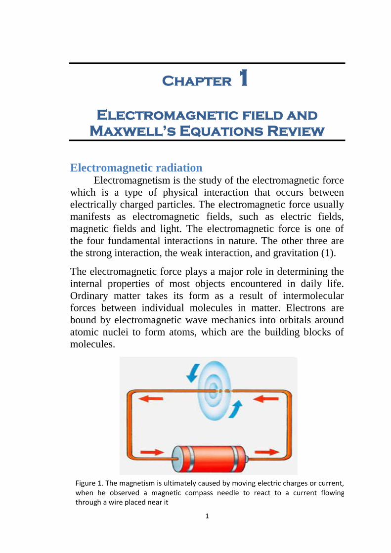
Figure 1. The magnetism is ultimately caused by moving electric charges or current, when he observed a magnetic compass needle to react to a current flowing through a wire placed near it
2
This governs the processes involved in chemistry, which arise
from interactions between the electrons of neighboring atoms,
which are in turn determined by the interaction between
electromagnetic force and the momentum of the electrons. There
are numerous mathematical descriptions of the electromagnetic
field. In classical electrodynamics, electric fields are described
as electric potential and electric current in Ohm's law, magnetic
fields are associated with electromagnetic induction and
magnetism, and Maxwell's equations describe how electric and
magnetic fields are generated and altered by each other and by
charges and currents (2).
The theoretical implications of electromagnetism, in particular
the establishment of the speed of light based on properties of the
"medium" of propagation (permeability and permittivity), led to
the development of special relativity by Albert Einstein in 1905.
Although electromagnetism is considered one of the four
fundamental forces, at high energy the weak force and
electromagnetism are unified. In the history of the universe,
during the quark epoch, the electroweak force split into the
electromagnetic and weak forces.
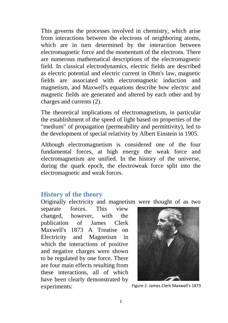
History of the theory Originally electricity and magnetism were thought of as two
separate forces. This view
changed, however, with the
publication of James Clerk
Maxwell's 1873 A Treatise on
Electricity and Magnetism in
which the interactions of positive
and negative charges were shown
to be regulated by one force. There
are four main effects resulting from
these interactions, all of which
have been clearly demonstrated by
experiments: Figure 2. James Clerk Maxwell's 1873
3
1. Electric charges attract or repel one another with a force
inversely proportional to the square of the distance
between them: unlike charges attract, like ones repel.
2. Magnetic poles (or states of polarization at individual
points) attract or repel one another in a similar way and
always come in pairs: every north pole is yoked to a south
pole.
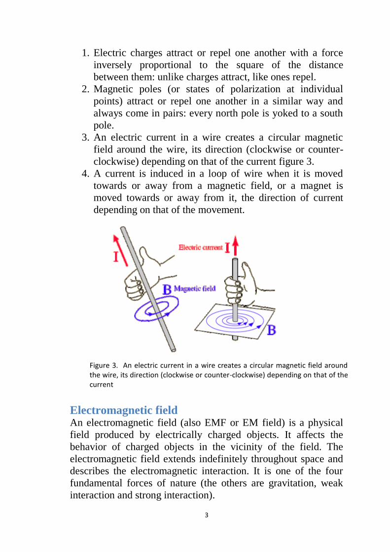
3. An electric current in a wire creates a circular magnetic
field around the wire, its direction (clockwise or counter-
clockwise) depending on that of the current figure 3.
4. A current is induced in a loop of wire when it is moved
towards or away from a magnetic field, or a magnet is
moved towards or away from it, the direction of current
depending on that of the movement.
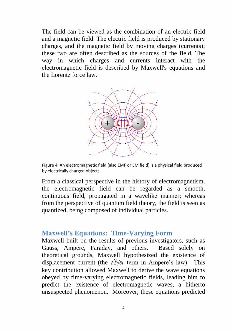
Electromagnetic field An electromagnetic field (also EMF or EM field) is a physical
field produced by electrically charged objects. It affects the
behavior of charged objects in the vicinity of the field. The
electromagnetic field extends indefinitely throughout space and
describes the electromagnetic interaction. It is one of the four
fundamental forces of nature (the others are gravitation, weak
interaction and strong interaction).
Figure 3. An electric current in a wire creates a circular magnetic field around the wire, its direction (clockwise or counter-clockwise) depending on that of the current
4
The field can be viewed as the combination of an electric field
and a magnetic field. The electric field is produced by stationary
charges, and the magnetic field by moving charges (currents);
these two are often described as the sources of the field. The
way in which charges and currents interact with the
electromagnetic field is described by Maxwell's equations and
the Lorentz force law.
From a classical perspective in the history of electromagnetism,
the electromagnetic field can be regarded as a smooth,
continuous field, propagated in a wavelike manner; whereas
from the perspective of quantum field theory, the field is seen as
quantized, being composed of individual particles.
Maxwell’s Equations: Time-Varying Form Maxwell built on the results of previous investigators, such as
Gauss, Ampere, Faraday, and others. Based solely on
theoretical grounds, Maxwell hypothesized the existence of
displacement current (the Dur
t term in Ampere’s law). This
key contribution allowed Maxwell to derive the wave equations
obeyed by time-varying electromagnetic fields, leading him to
predict the existence of electromagnetic waves, a hitherto
unsuspected phenomenon. Moreover, these equations predicted
Figure 4. An electromagnetic field (also EMF or EM field) is a physical field produced by electrically charged objects
5
that the hypothesized electromagnetic waves should propagate
with a velocity that is equal to the then-familiar value of the
speed of light. This, in turn, led Maxwell to assert that light is
an electromagnetic phenomenon. A dozen years later, Oliver
Heaviside cast Maxwell’s equations in their now-familiar vector
form, and a full seventeen years after Maxwell’s publication,
Heinrich Hertz performed the first experiments to validate
Maxwell’s theory. Maxwell’s original work stands to this day as
one of the prime examples of success of the predictive powers of
mathematical physics (3).
Maxwell’s Equations (general differential)
E B
t [1. a]
D ˜ [1. b]
H J D
t [1. c]
B 0 [1. d]
Where:
D= Electric flux density = 0E
E= Electric field in Volts/meter
B= Magnetic flux density = 0H
H= Magnetic field in Amps/meter
0= Free space permittivity= 8.85 x 10⁻¹²
0= Free space permeability= 4 x 10⁻⁷
Integral Form of Maxwell’s Equations
Most introductory books present Maxwell’s equations one at a time from an historical perspective. We find it convenient here to use an “axiomatic” approach, and present them all at once. We begin with the most general case: the integral form of
6
Maxwell’s equations for general time-varying fields in any medium. The time-varying electromagnetic source and field quantities are mathematically related by the following equations:
E C dl
B
t ds
S [1.2 a]
D S ds dv
V [1.2 b]
H C dl J ds
S D
t ds
S [1.2 c]
B S ds 0 [1.2 d]
Electromagnetic radiation
Electromagnetic radiation (EM radiation or EMR) is a form of
radiant energy released by certain electromagnetic processes.
Visible light is one type of electromagnetic radiation, other
familiar forms are invisible electromagnetic radiations such as
X-rays and radio waves.
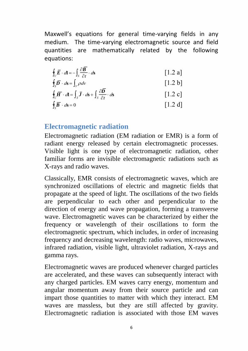
Classically, EMR consists of electromagnetic waves, which are
synchronized oscillations of electric and magnetic fields that
propagate at the speed of light. The oscillations of the two fields
are perpendicular to each other and perpendicular to the
direction of energy and wave propagation, forming a transverse
wave. Electromagnetic waves can be characterized by either the
frequency or wavelength of their oscillations to form the
electromagnetic spectrum, which includes, in order of increasing
frequency and decreasing wavelength: radio waves, microwaves,
infrared radiation, visible light, ultraviolet radiation, X-rays and
gamma rays.
Electromagnetic waves are produced whenever charged particles
are accelerated, and these waves can subsequently interact with
any charged particles. EM waves carry energy, momentum and
angular momentum away from their source particle and can
impart those quantities to matter with which they interact. EM
waves are massless, but they are still affected by gravity.
Electromagnetic radiation is associated with those EM waves
7
that are free to propagate themselves ("radiate") without the
continuing influence of the moving charges that produced them,
because they have achieved sufficient distance from those
charges. Thus, EMR is sometimes referred to as the far field. In
this jargon, the near field refers to EM fields near the charges
and current that directly produced them, as (for example) with
simple magnets, electromagnetic induction and static electricity
phenomena.
In the quantum theory of electromagnetism, EMR consists of
photons, the elementary particles responsible for all
electromagnetic interactions. Quantum effects provide additional
sources of EMR, such as the transition of electrons to lower
energy levels in an atom and black-body radiation. The energy
of an individual photon is quantized and is greater for photons of
higher frequency. This relationship is given by Planck's equation
E=hν,
where E is the energy per photon, ν is the frequency of the
photon, and h is Planck's constant. A single gamma ray photon,
for example, might carry ~100,000 times the energy of a single
photon of visible light.
The effects of EMR upon biological systems (and also to many
other chemical systems, under standard conditions) depend both
upon the radiation's power and its frequency. For EMR of visible
frequencies or lower (i.e., radio, microwave, infrared), the
damage done to cells and other materials is determined mainly
by power and caused primarily by heating effects from the
combined energy transfer of many photons. By contrast, for
Figure 5. The Electromagnetic plane wave.
8
ultraviolet and higher frequencies (i.e., X-rays and gamma rays),
chemical materials and living cells can be further damaged
beyond that done by simple heating, since individual photons of
such high frequency have enough energy to cause direct
molecular damage.
Electromagnetic spectrum
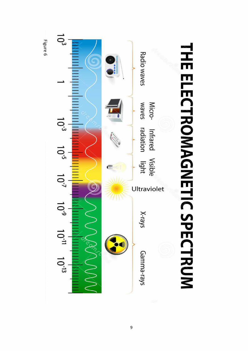
The electromagnetic spectrum is the range of all possible
frequencies of electromagnetic radiation. The "electromagnetic
spectrum" of an object has a different meaning, and is instead
the characteristic distribution of electromagnetic radiation
emitted or absorbed by that particular object.
The electromagnetic spectrum extends from below the low
frequencies used for modern radio communication to gamma
radiation at the short-wavelength (high-frequency) end, thereby
covering wavelengths from thousands of kilometers down to a
fraction of the size of an atom. The limit for long wavelengths is
the size of the universe itself, while it is thought that the short
wavelength limit is in the vicinity of the Planck length (4). Until
the middle of last century it was believed by most physicists that
this spectrum was infinite and continuous.
Most parts of the electromagnetic spectrum are used in science
for spectroscopic and other probing interactions, as ways to
study and characterize matter (5). In addition, radiation from
various parts of the spectrum has found many other uses for
communications and manufacturing (see electromagnetic
radiation for more applications).
9
Figure 6
10
What is Electromagnetic Shielding?
Electromagnetic shielding is designed to limit the influence of
electromagnetic fields and radiation on a device or object. The
process uses a barrier made from conductive material containing
electric charges of either positive or negative properties at the
subatomic particle level. Usually, this material is used to
separate the electrical components on the inside of the device
from the outside world. Cables also utilize the concept to
separate wires from outside environments. When used to block
radio frequencies, it is known as RF shielding.
The exact purpose of this shielding is to protect devices from the
coupling effect, the transfer of one form of energy to a device
that uses a different form. This is commonly caused by radio
waves, electrostatic fields, and the full spectrum of
electromagnetic radiation. The full level of protection is based
on the amount of reduction to the electric and magnetic fields.
This depends on the size, shape and orientation of the shielding.
No matter the standards in place, however, shielding cannot
protect against low-frequency magnetic fields. (6)
A variety of materials can be used as electromagnetic shielding
to protect an electrical device. Examples include ionized gas in
the form of plasma, metal foam with gas-filled pores, or simply
sheet metal. In order for holes within the shielding to be present,
they must be considerably smaller than any wavelength from the
electromagnetic field. If the shielding contains any openings
larger than the wavelength, it cannot effectively prevent the
device from becoming compromised.
Household devices often use a different shielding method due to
the likelihood of exposure to electromagnetic fields. Plastic
enclosures usually use some sort of metallic ink consisting of
copper or nickel in a small particular state. This material can be
sprayed onto the enclosure, producing a conductive layer of
metal that acts as protection. The main reason this layer works is
due to its close proximity to the grounding of the device.
11
Many common day-to-day items contain electromagnetic
shielding. One of the most common examples of this is the
microwave oven found within most kitchens in the United
States. With the metal housing working in unison with the
screen on the window, a Faraday cage is created. While some
visible light is able to pass through the window screen, waves of
other frequencies cannot.
History of the Shielding
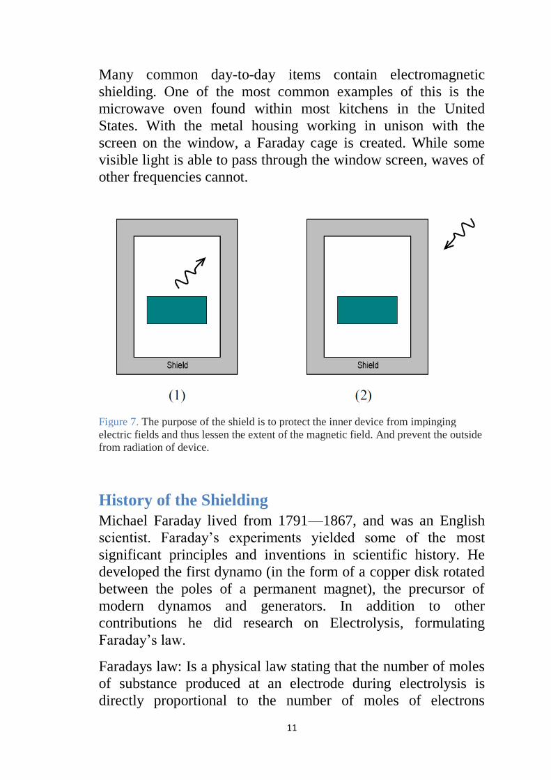
Michael Faraday lived from 1791—1867, and was an English
scientist. Faraday’s experiments yielded some of the most
significant principles and inventions in scientific history. He
developed the first dynamo (in the form of a copper disk rotated
between the poles of a permanent magnet), the precursor of
modern dynamos and generators. In addition to other
contributions he did research on Electrolysis, formulating
Faraday’s law.
Faradays law: Is a physical law stating that the number of moles
of substance produced at an electrode during electrolysis is
directly proportional to the number of moles of electrons
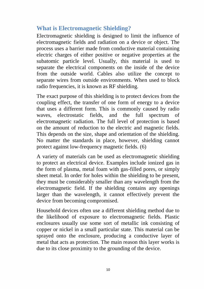
Figure 7. The purpose of the shield is to protect the inner device from impinging
electric fields and thus lessen the extent of the magnetic field. And prevent the outside
from radiation of device.
12
transferred at that electrode; the law is named for Michael
Faraday, who formulated it in 1834. The amount of electric
charge carried by one mole of electrons (6.02 x 10²³ electrons)
is called the faraday and is equal to 96,500 coulombs. The
number of faradays required to produce one mole of substance at
an electrode depends upon the way in which the substance is
oxidized or reduced.
Faraday Cage:
The Faraday cage was originally designed to demonstrate the
principles of static electricity, and thus allow the user to
investigate and manipulate the electrostatic phenomena.
Generally, a Faraday cage consists of an Iron mesh or Copper
mesh completely surrounding a square wooden housing or
cylinder. The Faraday cage originally proved that static
electricity can be controlled within an ungrounded cage that is
bonded to the structure in a continuous 360 degree manner (7).
Figure 8. Michael Faraday lived from 1791—1867, and was an English scientist.
13
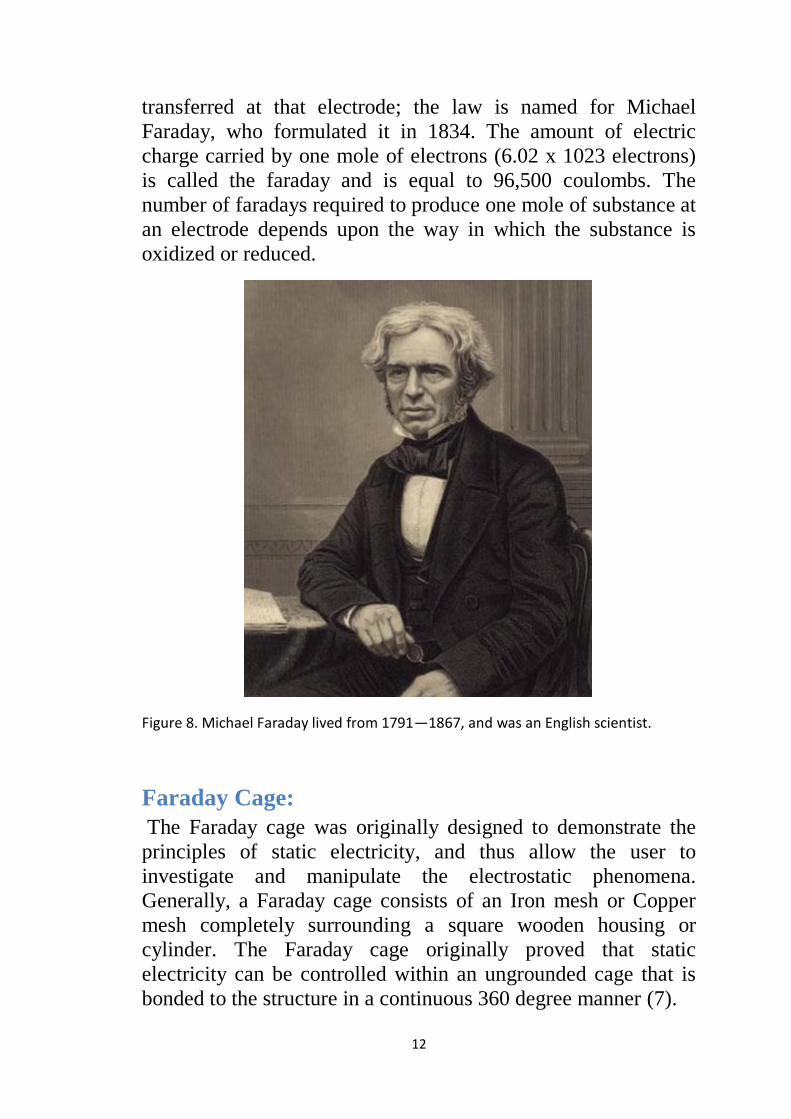
A Faraday cage operates because an external static electrical
field causes the electric charges within the cage's conducting
material to be distributed such that they cancel the field's effect
in the cage's interior. This phenomenon is used, for example, to
protect electronic equipment from lightning strikes and
electrostatic discharges.
Faraday cages cannot block static or slowly varying magnetic
fields, such as the Earth's magnetic field (a compass will still
work inside). To a large degree, though, they shield the interior
from external electromagnetic radiation if the conductor is thick
Figure 9. The Faraday cage
14
enough and any holes are significantly smaller than the
wavelength of the radiation. For example, certain computer
forensic test procedures of electronic systems that require an
environment free of electromagnetic interference can be carried
out within a screened room. These rooms are spaces that are
completely enclosed by one or more layers of a fine metal mesh
or perforated sheet metal. The metal layers are grounded to
dissipate any electric currents generated from external or internal
electromagnetic fields, and thus they block a large amount of the
electromagnetic interference. See also electromagnetic shielding.
The reception or transmission of radio waves, a form of
electromagnetic radiation, to or from an antenna within a
Faraday cage is heavily attenuated or blocked by the cage.
Shielding Materials
Today, because the synthesis of new materials is a very active
field of research and industrial development, the arsenal of
materials available for the realization of shielding structures is
always increasing. This chapter provides a review of the
properties of materials whose technology is mature enough that
they may be considered almost on the shelf. Materials that are
still ongoing development or whose present costs discourage
widespread use are considered in the last section, with the
caution that can be inferred when a situation is destined to
change over time.
Permeability and Permittivity
Permeability
A material’s permeability, μ, also called magnetic permeability,
is a constant of proportionality that exists between magnetic
induction (B) and magnetic field intensity (H). That is, B = μH.
This constant is equal to approximately 1.257 × 10⁻⁶
H/m in free
space (a vacuum), which is symbolized μo. The relative
15
permeability of materials is defined as μr = μ/μo. Materials with a
μr < 1, are called diamagnetic. When 1 < μr < 10, the materials
are called paramagnetic; when μr > 10, the materials are called
ferromagnetic. The permeability of some materials changes with
variation of temperature, intensity, and frequency of the applied
magnetic field. Certain ferromagnetics, especially powdered or
laminated iron, steel, or nickel alloys, have μr that can range up
to about 1,000,000. When a paramagnetic or ferromagnetic core
is inserted into a coil, the inductance is multiplied by μr
compared with the inductance of the same coil with an air core.
This effect is useful in the design of transformers and chokes for
alternating currents (AC), audio frequencies (AF), and radio
frequencies (RF) (8).
Permittivity
Permittivity, ε, also called electric permittivity, is a constant of
proportionality that exists between electric displacement (D) and
electric field intensity (E): D = εE. The vacuum permittivity is
ε0 = 1/(c2μ0) ≈ 8.85 × 10
-12 farad per meter (F/m), where c is the
speed of light and μ0 is the permeability of vacuum. The linear
permittivity of a homogeneous material is usually given relative
to that of vacuum, as a relative permittivity εr: εr = ε/εo. When εr
is greater than 1, these substances are generally called dielectric
materials, or dielectrics, such as glass, paper, mica, various
ceramics, polyethylene, and certain metal oxides. A high
permittivity tends to reduce any electric field present. For
instance, the capacitance of a capacitor can be raised by
increasing the permittivity of the dielectric material. Dielectrics
are generally used in capacitors and transmission lines in
filtering EMI by AC, AF, and RF (8).
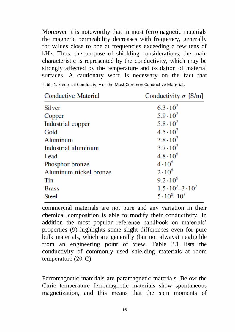
Standard Metallic And Ferromagnetic Materials
Most shielding structures are fabricated by means of standard
(i.e., nonmagnetic), conductive materials or by means of
ferromagnetic materials, which are often preferred for their
mechanical properties rather than their ferromagnetic behavior.
16
Moreover it is noteworthy that in most ferromagnetic materials
the magnetic permeability decreases with frequency, generally
for values close to one at frequencies exceeding a few tens of
kHz. Thus, the purpose of shielding considerations, the main
characteristic is represented by the conductivity, which may be
strongly affected by the temperature and oxidation of material
surfaces. A cautionary word is necessary on the fact that
commercial materials are not pure and any variation in their
chemical composition is able to modify their conductivity. In
addition the most popular reference handbook on materials’
properties (9) highlights some slight differences even for pure
bulk materials, which are generally (but not always) negligible
from an engineering point of view. Table 2.1 lists the
conductivity of commonly used shielding materials at room
temperature (20 C).
Ferromagnetic materials are paramagnetic materials. Below the
Curie temperature ferromagnetic materials show spontaneous
magnetization, and this means that the spin moments of
Table 1. Electrical Conductivity of the Most Common Conductive Materials
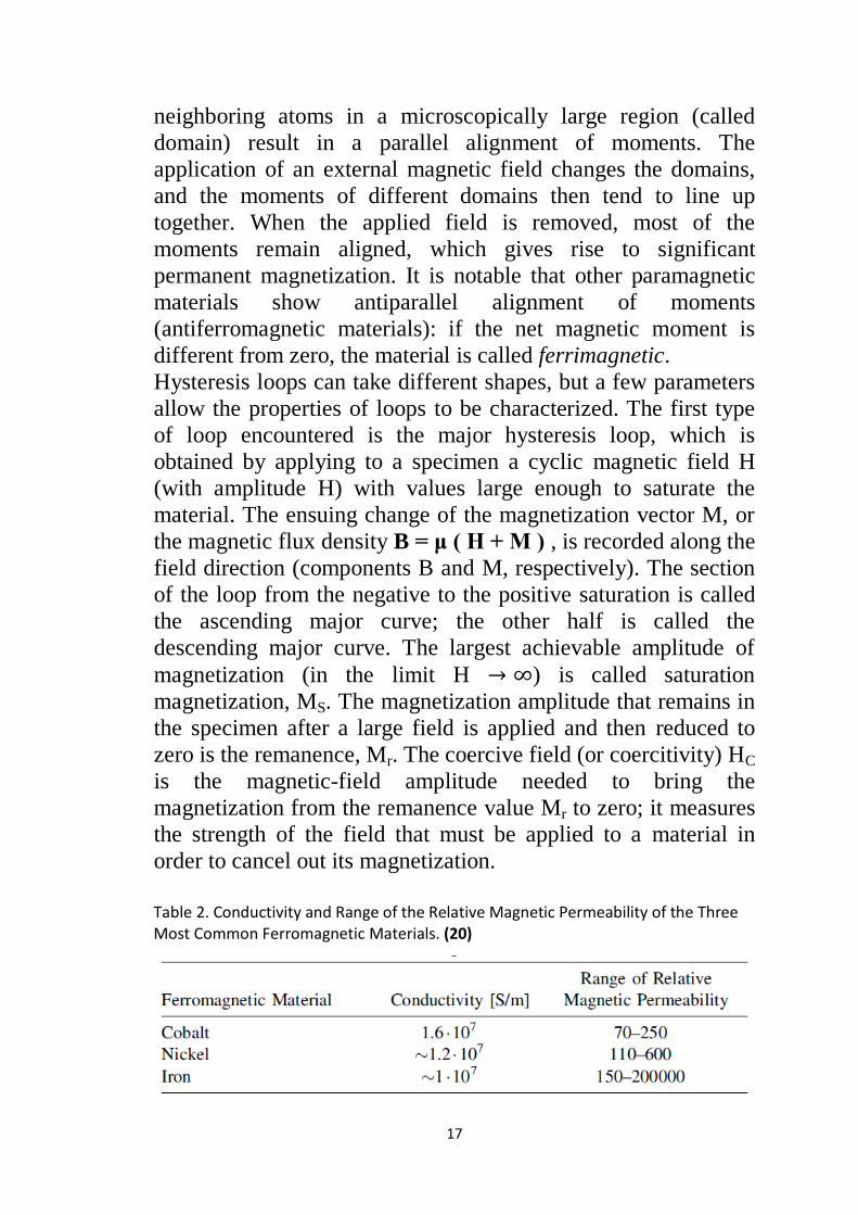
17
neighboring atoms in a microscopically large region (called
domain) result in a parallel alignment of moments. The
application of an external magnetic field changes the domains,
and the moments of different domains then tend to line up
together. When the applied field is removed, most of the
moments remain aligned, which gives rise to significant
permanent magnetization. It is notable that other paramagnetic
materials show antiparallel alignment of moments
(antiferromagnetic materials): if the net magnetic moment is
different from zero, the material is called ferrimagnetic.
Hysteresis loops can take different shapes, but a few parameters
allow the properties of loops to be characterized. The first type
of loop encountered is the major hysteresis loop, which is
obtained by applying to a specimen a cyclic magnetic field H
(with amplitude H) with values large enough to saturate the
material. The ensuing change of the magnetization vector M, or
the magnetic flux density B = μ ( H + M ) , is recorded along the
field direction (components B and M, respectively). The section
of the loop from the negative to the positive saturation is called
the ascending major curve; the other half is called the
descending major curve. The largest achievable amplitude of
magnetization (in the limit H ) is called saturation
magnetization, MS. The magnetization amplitude that remains in
the specimen after a large field is applied and then reduced to
zero is the remanence, Mr. The coercive field (or coercitivity) HC
is the magnetic-field amplitude needed to bring the
magnetization from the remanence value Mr to zero; it measures
the strength of the field that must be applied to a material in
order to cancel out its magnetization.
Table 2. Conductivity and Range of the Relative Magnetic Permeability of the Three Most Common Ferromagnetic Materials. (20)
18
Chapter 2
How Shielding Actually Works
Introduction
In chapter one I give brief introduction about shielding and
history, in this chapter I will discuss shielding in detail. The
important things and we must every time remember the purpose
of shielding are:
1. prevent the electronic devices inside the shield from
radiating emissions efficiently and/or
2. prevent the electromagnetic fields external to the device
from coupling efficiently to the electronics inside the
shield.
Types of EM Fields
In analyzing shielding it is helpful to consider the three types of
fields that occur. These different field types explain why the
same shield can behave differently under different operating
conditions.
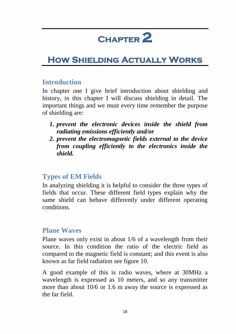
Plane Waves
Plane waves only exist in about 1/6 of a wavelength from their
source. In this condition the ratio of the electric field as
compared to the magnetic field is constant; and this event is also
known as far field radiation see figure 10.
A good example of this is radio waves, where at 30MHz a
wavelength is expressed as 10 meters, and so any transmitter
more than about 10/6 or 1.6 m away the source is expressed as
the far field.
19
Figure 10. (a) An diagram of a plain wave ,E electric field H magnetic field
(b) In electromagnetic radiation (such as microwaves from an antenna, shown here) the term
applies only to the parts of the electromagnetic field that radiate into infinite space and
decrease in intensity by aninverse-square law of power, so that the total radiation energy that
crosses through an imaginary spherical surface is the same, no matter how far away from the
antenna the spherical surface is drawn. Electromagnetic radiation thus includes thefar
field part of the electromagnetic field around a transmitter. A part of the "near-field" close to
the transmitter, forms part of the changingelectromagnetic field, but does not count as
electromagnetic radiation.
20
Electric Fields (E-Fields)
If the energy field is less than 1/6 of a wavelength from a high
impedance source, then the wave impedance is known as near
field source; and thus a capacitive energy dominates the field
during the near field effect, and this is because of the higher
wave impedances, thus the EM loss tends to be greater. This is
why it is possible to do more effective shielding from these
impinging electric fields.
A simpler way of looking at this effect is to understand that the
culprit electric fields produce voltages onto the victim circuitry.
For instance, if you suspect that a given analog interconnect is
producing an EMI event, then try disconnecting the wiring from
the circuit driving the line, and then short the signal pair
together; any voltage differential should be shorted out and the
input should quiet down, confirming that the electric field
produced was the culprit.
Magnetic Fields (H Fields)
If you are too close to a low impedance source, or a current
source, then a near field energy source is produced; but what
differs in this case, is that the inductive energy predominates.
Reflection losses are much less effective here due to lower wave
impedances and this effect continues as you drop in frequency;
So, this is the main reason why shielding becomes less effective
against low frequency magnetic fields, and why at this point in
your design balanced circuits of twist pair wires are so
important.
Another way of looking at this effect is that magnetic fields
produce currents over and onto their victim circuits. If you
suspect that a given analog interconnect is magnetic field, then
try disconnecting the wiring from the circuit driving the line and
leaving the signal pair open; any current flowing should be
stopped, this will confirm magnetic field coupling. The
application of MU-Metal to cover transformer windings will
cancel magnetic field disturbances in most cases.
21
What is EMI and EMC
Electromagnetic interference (EMI)
EMI is an unwanted disturbance that affects an electrical circuit
due to electromagnetic radiation emitted from an external
source. The disturbance may interrupt, obstruct, or otherwise
degrade or limit the effective performance of the circuit. The
source may be any object, artificial or natural, that carries
rapidly changing electrical currents, such as an electrical circuit,
the Sun or the Northern lights.
EMI can be induced intentionally for radio jamming, as in some
forms of electronic warfare, or unintentionally, as a result of
spurious emissions and responses, intermodulation products, and
the like. It frequently affects the reception of AM radio in urban
areas. It can also affect cell phone, FM radio and television
reception, although to a lesser extent.
Electromagnetic compatibility (EMC)
EMC is the branch of electrical sciences which studies the
unintentional generation, propagation and reception of
electromagnetic energy with reference to the unwanted effects
(Electromagnetic Interference, or EMI) that such energy may
induce. The goal of EMC is the correct operation, in the same
electromagnetic environment, of different equipment which uses
electromagnetic phenomena, and the avoidance of any
interference effects. In order to achieve this, EMC pursues two
different kinds of issues. Emission issues are related to the
unwanted generation of electromagnetic energy by some source,
and to the countermeasures which should be taken in order to
reduce such generation and to avoid the escape of any remaining
energies into the external environment. Susceptibility or
immunity issues, in contrast, refer to the correct operation of
electrical equipment, referred to as the victim, in the presence of
unplanned electromagnetic disturbances. Interference, or noise,
mitigation and hence electromagnetic compatibility is achieved
22
primarily by addressing both emission and susceptibility issues,
i.e., quieting the sources of interference and hardening the
potential victims. The coupling path between source and victim
may also be separately addressed to increase its attenuation.
Shielding effectiveness
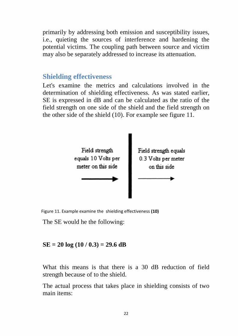
Let's examine the metrics and calculations involved in the
determination of shielding effectiveness. As was stated earlier,
SE is expressed in dB and can be calculated as the ratio of the
field strength on one side of the shield and the field strength on
the other side of the shield (10). For example see figure 11.
The SE would he the following:
SE = 20 log (10 / 0.3) = 29.6 dB
What this means is that there is a 30 dB reduction of field
strength because of to the shield.
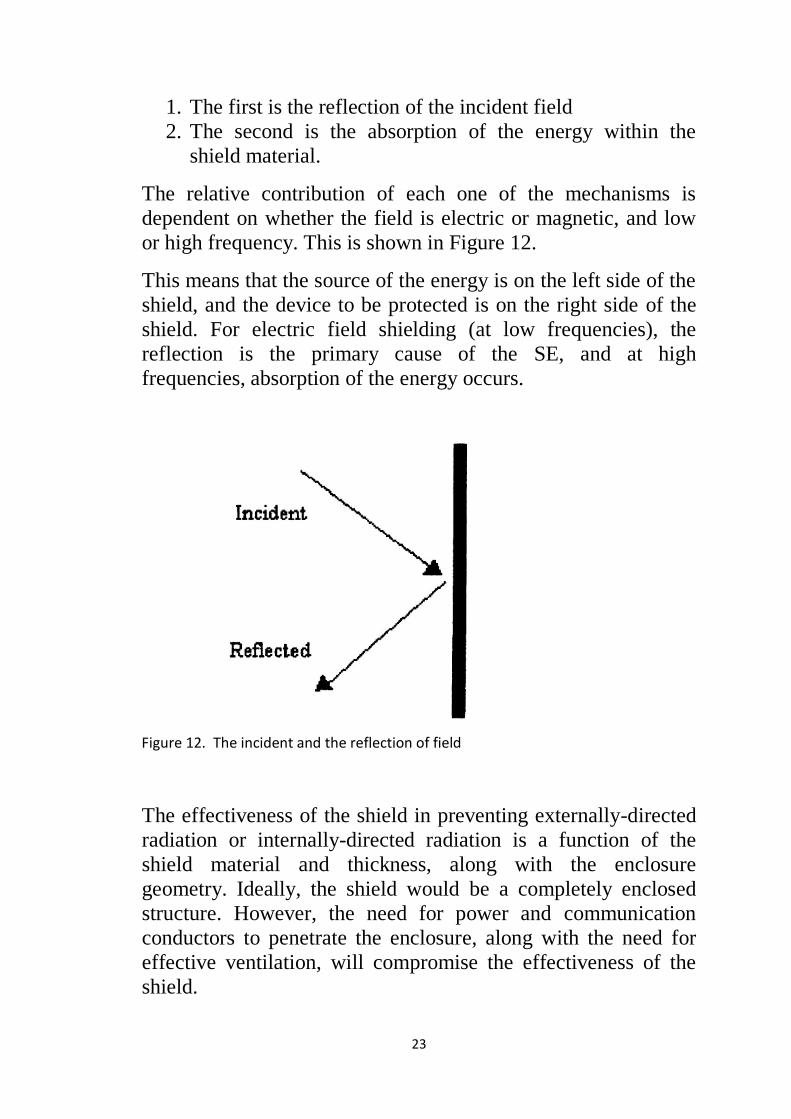
The actual process that takes place in shielding consists of two
main items:
Figure 11. Example examine the shielding effectiveness (10)
23
1. The first is the reflection of the incident field
2. The second is the absorption of the energy within the
shield material.
The relative contribution of each one of the mechanisms is
dependent on whether the field is electric or magnetic, and low
or high frequency. This is shown in Figure 12.
This means that the source of the energy is on the left side of the
shield, and the device to be protected is on the right side of the
shield. For electric field shielding (at low frequencies), the
reflection is the primary cause of the SE, and at high
frequencies, absorption of the energy occurs.
The effectiveness of the shield in preventing externally-directed
radiation or internally-directed radiation is a function of the
shield material and thickness, along with the enclosure
geometry. Ideally, the shield would be a completely enclosed
structure. However, the need for power and communication
conductors to penetrate the enclosure, along with the need for
effective ventilation, will compromise the effectiveness of the
shield.
Figure 12. The incident and the reflection of field
24
The shielding effectiveness is equivalent to that of insertion loss
in microwave circuits where the insertion loss of a given
component is typically defined as the ratio of the signal obtained
without the component in the circuit to the signal obtained with
the component in the circuit.
Key parameters in shield design (electric field)
Important parameters include the thickness of the material
sometimes known as the barrier thickness. It is important to
know what this is with respect to the skin depth at the particular
frequency of concern. If the thickness of the material is equal to
or much greater than the skin depth, then there is attenuation
within the material. If the thickness is equal to or less than the
skin depth, then the primary source of the SE is the reflection at
the interface between the field and the material.
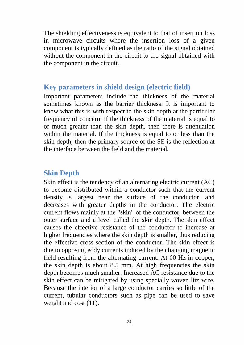
Skin Depth
Skin effect is the tendency of an alternating electric current (AC)
to become distributed within a conductor such that the current
density is largest near the surface of the conductor, and
decreases with greater depths in the conductor. The electric
current flows mainly at the "skin" of the conductor, between the
outer surface and a level called the skin depth. The skin effect
causes the effective resistance of the conductor to increase at
higher frequencies where the skin depth is smaller, thus reducing
the effective cross-section of the conductor. The skin effect is
due to opposing eddy currents induced by the changing magnetic
field resulting from the alternating current. At 60 Hz in copper,
the skin depth is about 8.5 mm. At high frequencies the skin
depth becomes much smaller. Increased AC resistance due to the
skin effect can be mitigated by using specially woven litz wire.
Because the interior of a large conductor carries so little of the
current, tubular conductors such as pipe can be used to save
weight and cost (11).
25
t
BE
EJ
t
DJH
Figure 13. Physical Explanation of Skin Effect
Then to find the skin depth:
2
where is the angular frequency of the fields and is the
conductor conductivity. See figure 14, represent thin shield.
It turns out that the thickness is important to the magnetic H
field shielding capability of a material. This is because of the
attenuation that takes place as the H field is passing through the
material. Attenuation occurs because the magnetic field induces
current in the material (a conductor), and these currents flow in a
circular pattern. This pattern is similar to those seen in water,
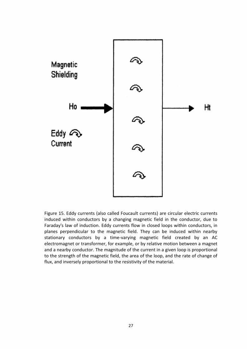
and are called Eddy currents. See Figure 15.
Another aspect is that these circulating currents also produce
heat, due to the I2R losses (this is an easy way to tell if a
transformer is working is by feeling if it's warm!)
The difficulty with shields is that they must be constructed and
maintained to ensure their integrity. If there are openings in the
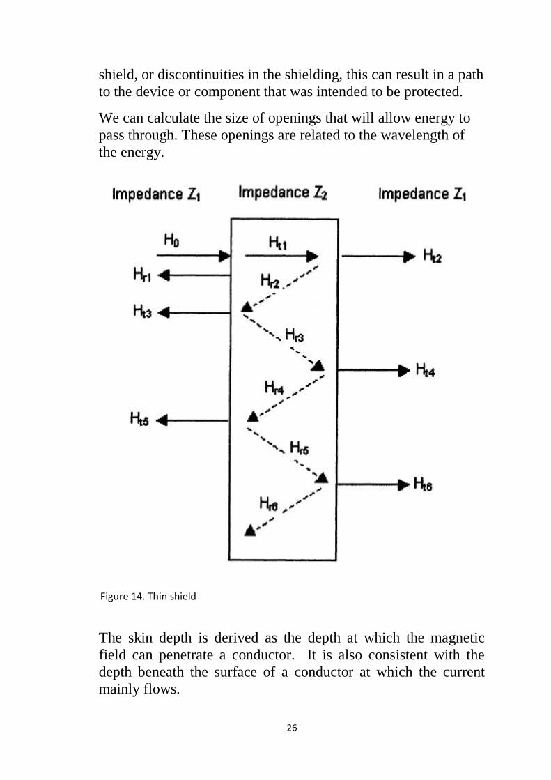
26
shield, or discontinuities in the shielding, this can result in a path
to the device or component that was intended to be protected.
We can calculate the size of openings that will allow energy to
pass through. These openings are related to the wavelength of
the energy.
The skin depth is derived as the depth at which the magnetic
field can penetrate a conductor. It is also consistent with the
depth beneath the surface of a conductor at which the current
mainly flows.
Figure 14. Thin shield
27
Figure 15. Eddy currents (also called Foucault currents) are circular electric currents induced within conductors by a changing magnetic field in the conductor, due to Faraday's law of induction. Eddy currents flow in closed loops within conductors, in planes perpendicular to the magnetic field. They can be induced within nearby stationary conductors by a time-varying magnetic field created by an AC electromagnet or transformer, for example, or by relative motion between a magnet and a nearby conductor. The magnitude of the current in a given loop is proportional to the strength of the magnetic field, the area of the loop, and the rate of change of flux, and inversely proportional to the resistivity of the material.
28
Chapter 3
Effectiveness of Single and
Malty Layers Shielding
Introduction
In this chapter I well discuses two important factors that mast be
noted when design good shielding the two factors are:
1. Reflection from surface layer
2. Absorption of layer.
Then I return to discuss the above factors for malty layers slab.
Plane Wave Propagation
In chapter two I give brief introduction about plane wave, in this
chapter I will discuss in detail.
Plane waves are not normally incident, so now we must consider
the general problem of a plane wave propagating along a
specified axis that is arbitrarily relative to a rectangular
coordinate system. The most convenient way is in terms of the
direction cosines of the uniform plane wave, the equiphase
surfaces are planes perpendicular to the direction of propagation.
Definitions:
uniform planes – a free space plane wave at an infinite
distance from the generator, having constant amplitude electric
and magnetic field vectors over the equiphase surfaces.
equiphase surface – any surface in a wave over which the
field vectors of a particular instant have either 0° or 180° phase
difference.
29
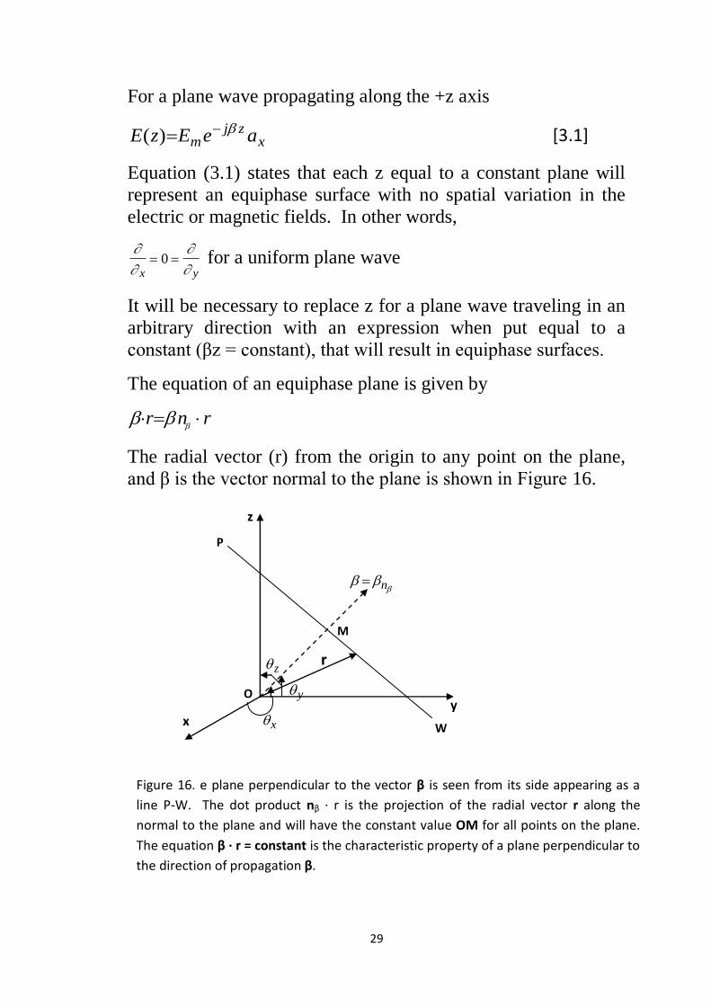
For a plane wave propagating along the +z axis
xzj
m aeEzE )( [3.1]
Equation (3.1) states that each z equal to a constant plane will
represent an equiphase surface with no spatial variation in the
electric or magnetic fields. In other words,
x y
0 for a uniform plane wave
It will be necessary to replace z for a plane wave traveling in an
arbitrary direction with an expression when put equal to a
constant (βz = constant), that will result in equiphase surfaces.
The equation of an equiphase plane is given by
rnr
The radial vector (r) from the origin to any point on the plane,
and β is the vector normal to the plane is shown in Figure 16.
x y
z
P
W
r
x
y
z
O
M
n
Figure 16. e plane perpendicular to the vector β is seen from its side appearing as a
line P-W. The dot product nβ · r is the projection of the radial vector r along the
normal to the plane and will have the constant value OM for all points on the plane.
The equation β · r = constant is the characteristic property of a plane perpendicular to
the direction of propagation β.
30
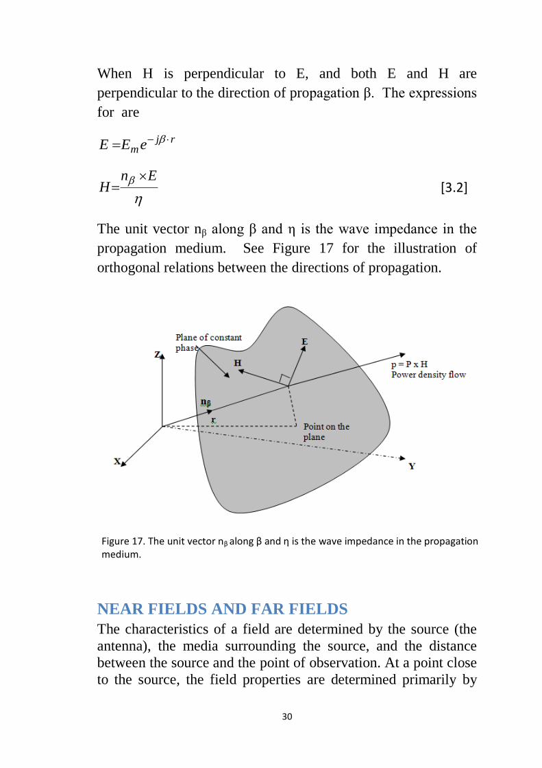
When H is perpendicular to E, and both E and H are
perpendicular to the direction of propagation β. The expressions
for are
rjmeEE
EnH
[3.2]
The unit vector nβ along β and η is the wave impedance in the
propagation medium. See Figure 17 for the illustration of
orthogonal relations between the directions of propagation.
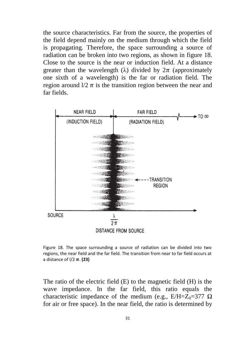
NEAR FIELDS AND FAR FIELDS
The characteristics of a field are determined by the source (the
antenna), the media surrounding the source, and the distance
between the source and the point of observation. At a point close
to the source, the field properties are determined primarily by
Figure 17. The unit vector nβ along β and η is the wave impedance in the propagation medium.
31
the source characteristics. Far from the source, the properties of
the field depend mainly on the medium through which the field
is propagating. Therefore, the space surrounding a source of
radiation can be broken into two regions, as shown in figure 18.
Close to the source is the near or induction field. At a distance
greater than the wavelength (λ) divided by 2 (approximately
one sixth of a wavelength) is the far or radiation field. The
region around l/2 is the transition region between the near and
far fields.
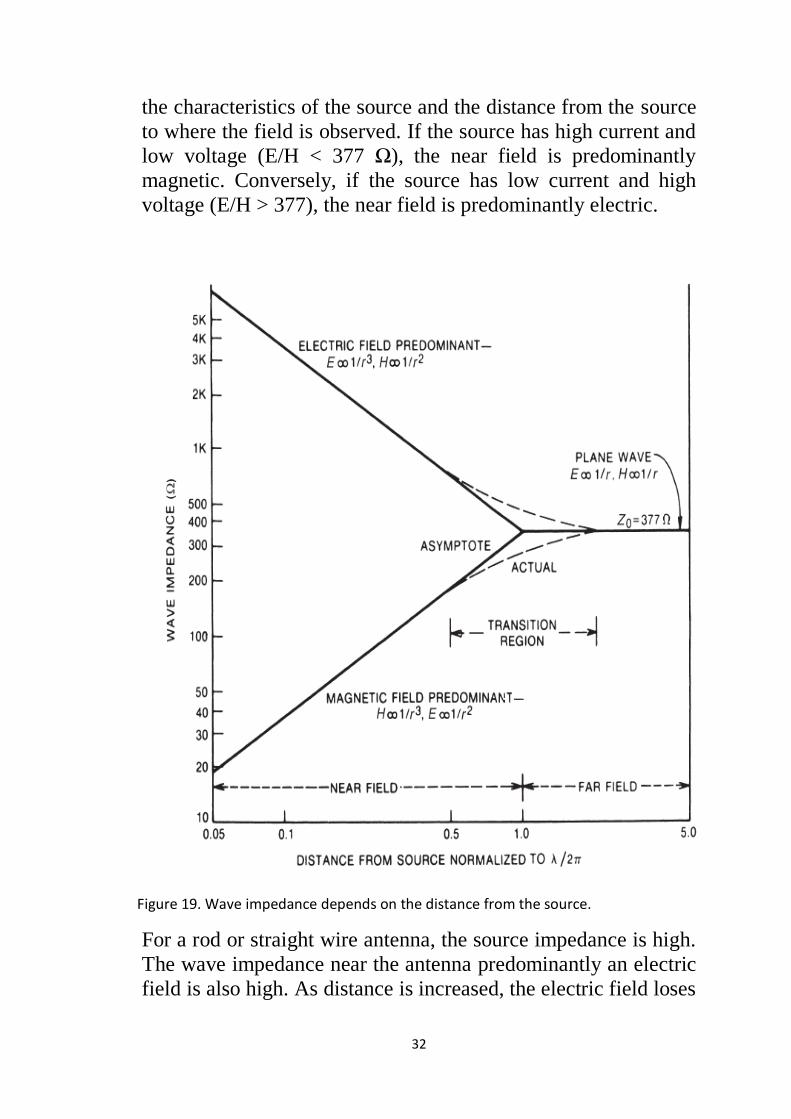
The ratio of the electric field (E) to the magnetic field (H) is the
wave impedance. In the far field, this ratio equals the
characteristic impedance of the medium (e.g., E/H=Z0=377 Ω
for air or free space). In the near field, the ratio is determined by
Figure 18. The space surrounding a source of radiation can be divided into two regions, the near field and the far field. The transition from near to far field occurs at a distance of l/2 𝝅. (23)
32
the characteristics of the source and the distance from the source
to where the field is observed. If the source has high current and
low voltage (E/H < 377 Ω), the near field is predominantly
magnetic. Conversely, if the source has low current and high
voltage (E/H > 377), the near field is predominantly electric.
For a rod or straight wire antenna, the source impedance is high.
The wave impedance near the antenna predominantly an electric
field is also high. As distance is increased, the electric field loses
Figure 19. Wave impedance depends on the distance from the source.
33
some of its intensity as it generates a complementary magnetic
field. In the near field, the electric field attenuates at a rate of
(1/r)3, whereas the magnetic field attenuates at a rate of (1/r)
2.
Thus, the wave impedance from a straight wire antenna
decreases with distance and asymptotically approaches the
impedance of free space in the far field, as shown in Figure 19.
For a predominantly magnetic field—such as produced by a loop
antenna the wave impedance near the antenna is low. As the
distance from the source increases, the magnetic field attenuates
at a rate of (1/r)3 and the electric field attenuates at a rate of
(1/r)2. The wave impedance therefore increases with distance
and approaches that of free space at a distance of l/2 . In the far
field, both the electric and magnetic fields attenuate at a rate of
1/r. In the near field the electric and magnetic fields must be
considered separately, because the ratio of the two is not
constant. In the far field, however, they combine to form a plane
wave having an impedance of 377 Ω. Therefore, when plane
waves are discussed, they are assumed to be in the far field.
When individual electric and magnetic fields are discussed, they
are assumed to be in the near field.
34
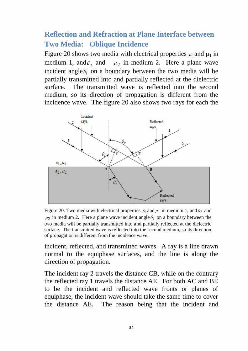
Reflection and Refraction at Plane Interface between
Two Media: Oblique Incidence
Figure 20 shows two media with electrical properties 1 and μ1 in
medium 1, and2
and 2 in medium 2. Here a plane wave
incident anglei on a boundary between the two media will be
partially transmitted into and partially reflected at the dielectric
surface. The transmitted wave is reflected into the second
medium, so its direction of propagation is different from the
incidence wave. The figure 20 also shows two rays for each the
incident, reflected, and transmitted waves. A ray is a line drawn
normal to the equiphase surfaces, and the line is along the
direction of propagation.
The incident ray 2 travels the distance CB, while on the contrary
the reflected ray 1 travels the distance AE. For both AC and BE
to be the incident and reflected wave fronts or planes of
equiphase, the incident wave should take the same time to cover
the distance AE. The reason being that the incident and
Figure 20. Two media with electrical properties and in medium 1, and and
in medium 2. Here a plane wave incident angle on a boundary between the
two media will be partially transmitted into and partially reflected at the dielectric
surface. The transmitted wave is reflected into the second medium, so its direction
of propagation is different from the incidence wave.
35
reflected wave rays are located in the same medium, therefore
their velocities will be equal,
AEnCBn 12 [3.3]
Or we can rewrite equation in this form:
ri ABAB sinsin
Where the n1 and n2 are the refractive index of medium one and
medium two, and the magnitude of the velocity n1 in medium 1
is:
111 n
And in medium 2:
221 n
Also,
i
i
ABAD
ABCB
sin
sin
Therefore,
11
22
sin
sin
t
i
AD
CB
For most dielectrics 12
Therefore,
211
2
sin
sin
t
i [3.4]
Equation [3.4] is known as Snell’s Law of Refraction.
36
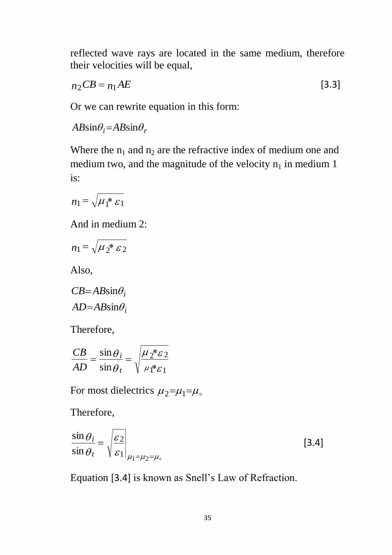
Single Dielectric Slab
Multiple interface problems can be handled in a straightforward
way with the help of the matching and propagation matrices. For
example, Figure 21 shows a two-interface problem with a
dielectric slab η1 separating the semi-infinite media ηa and ηb.
Let ρ1, ρ2 be the elementary reflection coefficients from the left
sides of the two interfaces, and let τ1, τ2 be the corresponding
transmission coefficients:
Figure 21. Single dielectric slab, Let l1 be the width of the slab, k1 = ω/c1 the
propagation wavenumber, and λ1 = 2π/k1 the corresponding wavelength within
the slab. We have λ1 = λ0/n1, where λ0 is the free-space wavelength and n1 the
refractive index of the slab. We assume the incident field is from the left medium
ηa, and thus, in medium ηb there is only a forward wave.
37
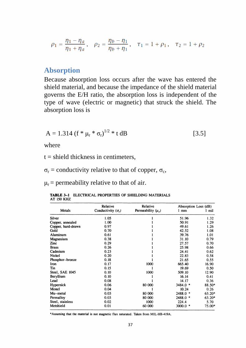
Absorption
Because absorption loss occurs after the wave has entered the
shield material, and because the impedance of the shield material
governs the E/H ratio, the absorption loss is independent of the
type of wave (electric or magnetic) that struck the shield. The
absorption loss is
A = 1.314 (f * μr * σr)1/2
* t dB [3.5]
where
t = shield thickness in centimeters,
σr = conductivity relative to that of copper, σc,
μr = permeability relative to that of air.
38
Table 3-1 gives the values of σr , μr and A for various metals.
Values of μr >> 1 for shield materials are only obtained up to
several hundred kilohertz. Beyond 500 kHz, μr = 1 for the
materials listed in the table . The last columns of the table give
the absorption loss at 150 kHz for both 1 mm and 1 mil (0.001
in.) thick sheets for the listed materials. The absorption loss for
other thicknesses can be calculated by simply multiplying by the
shield thickness in millimeters or mils (12).
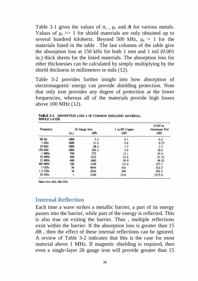
Table 3-2 provides further insight into how absorption of
electromagnetic energy can provide shielding protection. Note
that only iron provides any degree of protection at the lower
frequencies, whereas all of the materials provide high losses
above 100 MHz (12).
Internal Reflection
Each time a wave strikes a metallic barrier, a part of its energy
passes into the barrier, while part of the energy is reflected. This
is also true on exiting the barrier. Thus , multiple reflections
exist within the barrier. If the absorption loss is greater than 15
dB , then the effect of these internal reflections can be ignored.
A review of Table 3-2 indicates that this is the case for most
material above 1 MHz. If magnetic shielding is required, then
even a single-layer 26 gauge iron will provide greater than 15
39
dB of absorption loss down to 1 kHz. Thus, for practical
purposes, only the reflection and absorption losses need be
calculated in most shielding situations.
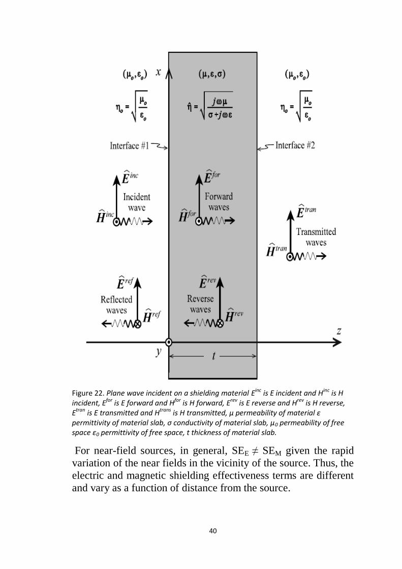
Case Study (single Slab)
The shielding effectiveness of a given shield is actually a
function of the distance from the incident wave source (near-
field sources and far-field sources). The source is initially
assumed to be a far-field source such that the incident wave can
be approximated by a normally-incident uniform plane wave. As
the incident wave encounters interface #1at z = 0, a portion of
the wave is reflected away from the interface, while the
remainder of the wave is transmitted into the metal, and is
attenuated as the wave travels through the metal. A portion of
forward wave in the metal is reflected from interface #2 at z = t
producing a reverse wave, while the remainder of the wave is
transmitted into the air region (z > t). The reflection/
transmission process at the two interfaces produces, in theory, an
infinite number of reflected, forward, reverse and transmitted
wave components.
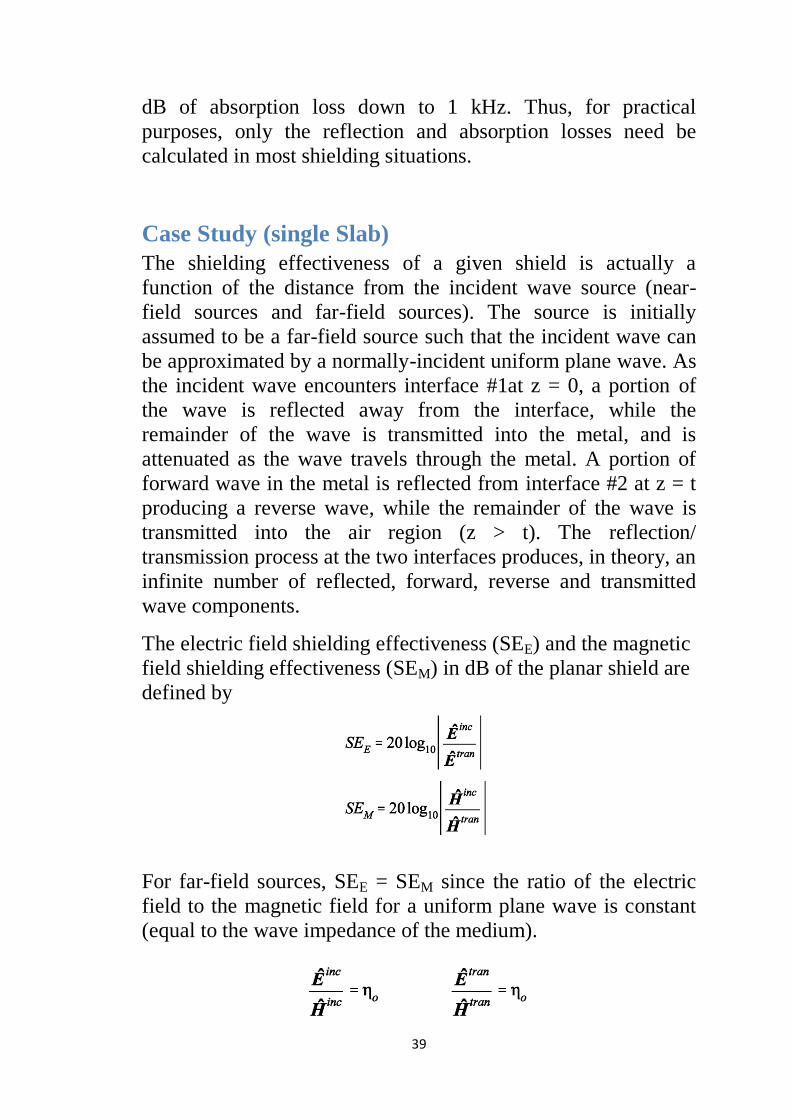
The electric field shielding effectiveness (SEE) and the magnetic
field shielding effectiveness (SEM) in dB of the planar shield are
defined by
For far-field sources, SEE = SEM since the ratio of the electric
field to the magnetic field for a uniform plane wave is constant
(equal to the wave impedance of the medium).
40
For near-field sources, in general, SEE ≠ SEM given the rapid
variation of the near fields in the vicinity of the source. Thus, the
electric and magnetic shielding effectiveness terms are different
and vary as a function of distance from the source.
Figure 22. Plane wave incident on a shielding material Einc is E incident and Hinc is H incident, Efor is E forward and Hfor is H forward, Erev is E reverse and Hrev is H reverse, Etran is E transmitted and Htrans is H transmitted, μ permeability of material ε permittivity of material slab, σ conductivity of material slab, μ0 permeability of free space ε0 permittivity of free space, t thickness of material slab.
41
The shielding effectiveness of the planar shield is governed by
three distinct mechanisms involving the interaction of the
incident wave with the air/conductor interfaces and the
conducting medium of the shield. These mechanisms are:
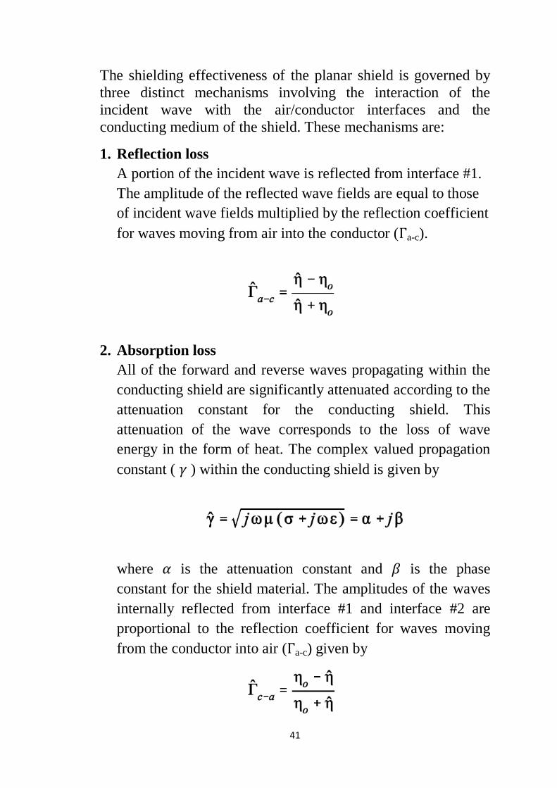
1. Reflection loss
A portion of the incident wave is reflected from interface #1.
The amplitude of the reflected wave fields are equal to those
of incident wave fields multiplied by the reflection coefficient
for waves moving from air into the conductor ( a-c).
2. Absorption loss
All of the forward and reverse waves propagating within the
conducting shield are significantly attenuated according to the
attenuation constant for the conducting shield. This
attenuation of the wave corresponds to the loss of wave
energy in the form of heat. The complex valued propagation
constant ( ) within the conducting shield is given by
where is the attenuation constant and is the phase
constant for the shield material. The amplitudes of the waves
internally reflected from interface #1 and interface #2 are
proportional to the reflection coefficient for waves moving
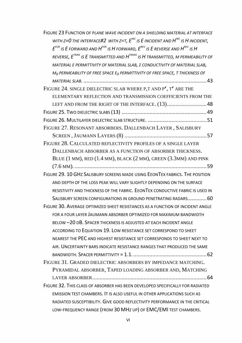
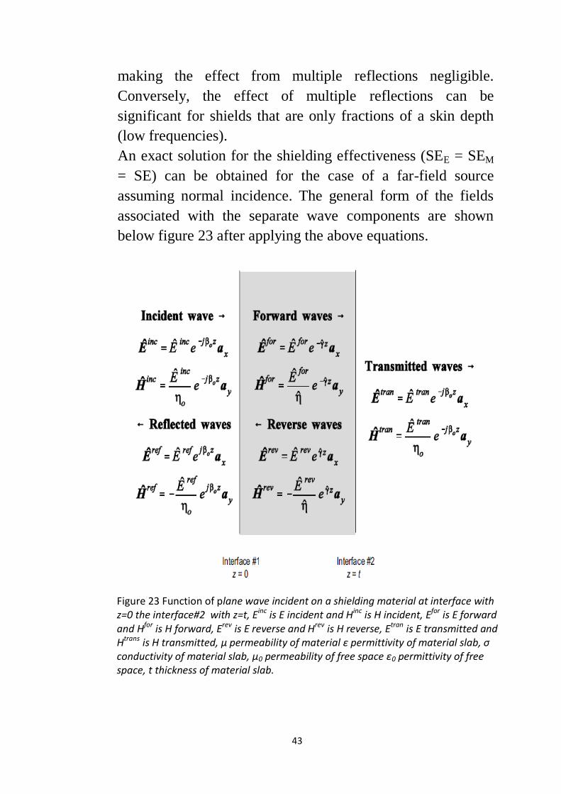
from the conductor into air ( a-c) given by
42
For good conductors, the attenuation constant can be
approximated by the inverse of the skin depth ( ).
The thickness of the shield relative to the skin depth (which is
a function of frequency) dictates how significantly the wave
is attenuated as it propagates through the shield.
3. Multiple reflections
A portion of each of the forward waves within the planar
shield is transmitted into the air region (z > t). The
transmitted fields used in the SE calculations are the vector
sum of the fields associated with these forward waves.
Likewise, a portion of each of the reverse waves within the
planar shield is transmitted into the air region (z < 0). The
reverse waves transmitted out of the planar shield represent
additional losses which enhance the shielding effectiveness
value. Both of these transmitted waves are proportional to the
transmission coefficient for waves moving from the
conductor to air ( a-c).
The significance of the multiple reflections is related to the
thickness of the planar shield relative to the skin depth. If the
shield is several skin depths thick, there is significant
attenuation as the initial wave progresses across the shield,
43
making the effect from multiple reflections negligible.
Conversely, the effect of multiple reflections can be
significant for shields that are only fractions of a skin depth
(low frequencies).
An exact solution for the shielding effectiveness (SEE = SEM
= SE) can be obtained for the case of a far-field source
assuming normal incidence. The general form of the fields
associated with the separate wave components are shown
below figure 23 after applying the above equations.
Figure 23 Function of plane wave incident on a shielding material at interface with z=0 the interface#2 with z=t, Einc is E incident and Hinc is H incident, Efor is E forward and Hfor is H forward, Erev is E reverse and Hrev is H reverse, Etran is E transmitted and Htrans is H transmitted, μ permeability of material ε permittivity of material slab, σ conductivity of material slab, μ0 permeability of free space ε0 permittivity of free space, t thickness of material slab.
44
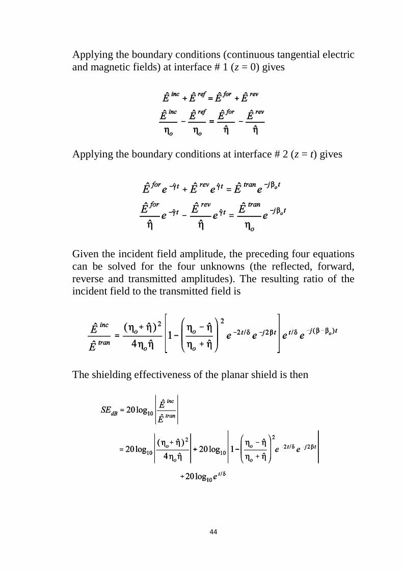
Applying the boundary conditions (continuous tangential electric
and magnetic fields) at interface # 1 (z = 0) gives
Applying the boundary conditions at interface # 2 (z = t) gives
Given the incident field amplitude, the preceding four equations
can be solved for the four unknowns (the reflected, forward,
reverse and transmitted amplitudes). The resulting ratio of the
incident field to the transmitted field is
The shielding effectiveness of the planar shield is then
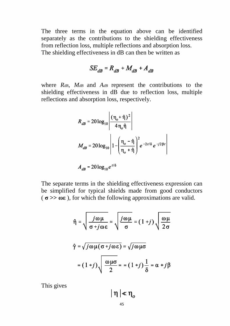
45
The three terms in the equation above can be identified
separately as the contributions to the shielding effectiveness
from reflection loss, multiple reflections and absorption loss.
The shielding effectiveness in dB can then be written as
where RdB, MdB and AdB represent the contributions to the
shielding effectiveness in dB due to reflection loss, multiple
reflections and absorption loss, respectively.
The separate terms in the shielding effectiveness expression can
be simplified for typical shields made from good conductors
( σ >> ωε ), for which the following approximations are valid.
This gives
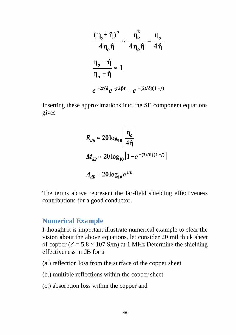
46
Inserting these approximations into the SE component equations
gives
The terms above represent the far-field shielding effectiveness
contributions for a good conductor.
Numerical Example
I thought it is important illustrate numerical example to clear the
vision about the above equations, let consider 20 mil thick sheet
of copper ( = 5.8 × 10⁷ S/m) at 1 MHz Determine the shielding
effectiveness in dB for a
(a.) reflection loss from the surface of the copper sheet
(b.) multiple reflections within the copper sheet
(c.) absorption loss within the copper and
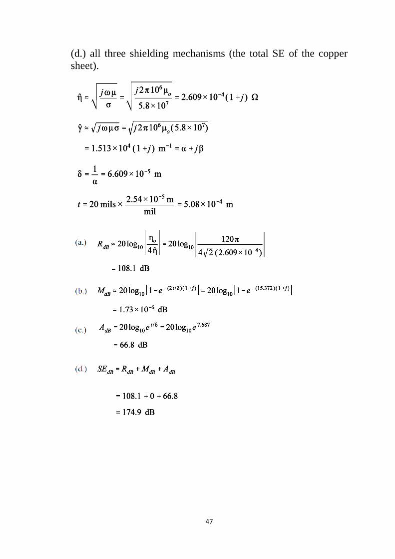
47
(d.) all three shielding mechanisms (the total SE of the copper
sheet).
48
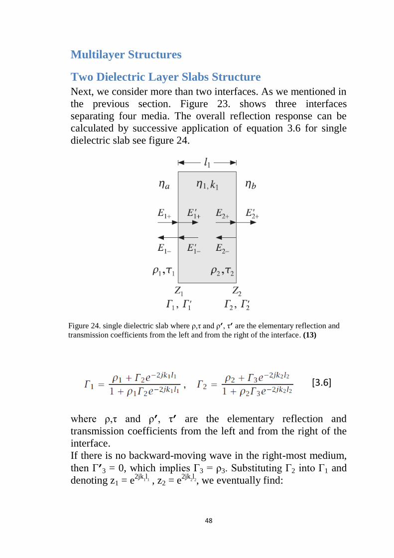
Multilayer Structures
Two Dielectric Layer Slabs Structure
Next, we consider more than two interfaces. As we mentioned in
the previous section. Figure 23. shows three interfaces
separating four media. The overall reflection response can be
calculated by successive application of equation 3.6 for single
dielectric slab see figure 24.
where ρ,τ and ρ’, τ’ are the elementary reflection and
transmission coefficients from the left and from the right of the
interface.
If there is no backward-moving wave in the right-most medium,
then Γ’3 = 0, which implies Γ3 = ρ3. Substituting Γ2 into Γ1 and
denoting z1 = e2jk
1l1 , z2 = e
2jk2l2, we eventually find:
Figure 24. single dielectric slab where ρ,τ and ρ’, τ’ are the elementary reflection and
transmission coefficients from the left and from the right of the interface. (13)
[3.6]
49
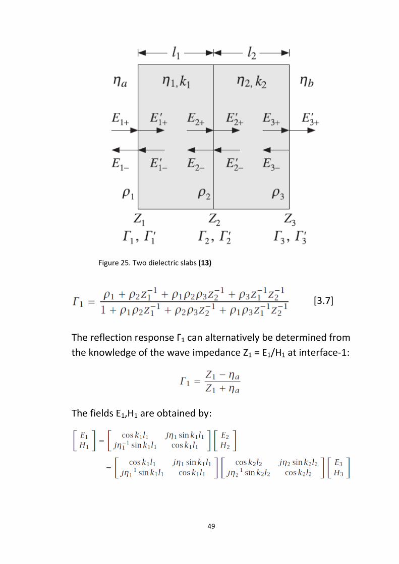
The reflection response Γ1 can alternatively be determined from
the knowledge of the wave impedance Z1 = E1/H1 at interface-1:
The fields E1,H1 are obtained by:
Figure 25. Two dielectric slabs (13)
[3.7]
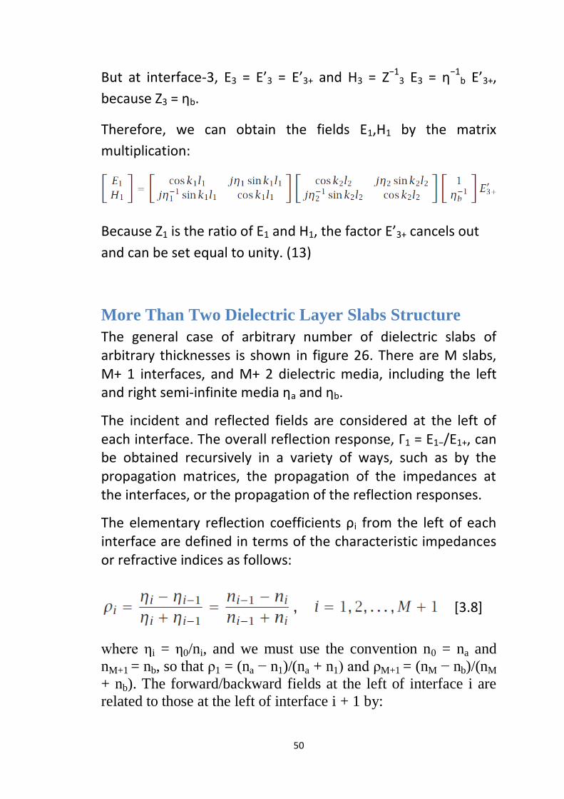
50
But at interface-3, E3 = E’3 = E’3+ and H3 = Z−13 E3 = η−1
b E’3+,
because Z3 = ηb.
Therefore, we can obtain the fields E1,H1 by the matrix
multiplication:
Because Z1 is the ratio of E1 and H1, the factor E’3+ cancels out
and can be set equal to unity. (13)
More Than Two Dielectric Layer Slabs Structure
The general case of arbitrary number of dielectric slabs of arbitrary thicknesses is shown in figure 26. There are M slabs, M+ 1 interfaces, and M+ 2 dielectric media, including the left and right semi-infinite media ηa and ηb.
The incident and reflected fields are considered at the left of each interface. The overall reflection response, Γ1 = E1−/E1+, can be obtained recursively in a variety of ways, such as by the propagation matrices, the propagation of the impedances at the interfaces, or the propagation of the reflection responses.
The elementary reflection coefficients ρi from the left of each interface are defined in terms of the characteristic impedances or refractive indices as follows:
where ηi = η0/ni, and we must use the convention n0 = na and
nM+1 = nb, so that ρ1 = (na − n1)/(na + n1) and ρM+1 = (nM − nb)/(nM
+ nb). The forward/backward fields at the left of interface i are
related to those at the left of interface i + 1 by:
[3.8]
51
Figure 26. M
ultilayer d
ielectric slab stru
cture.
52
where τi = 1+ρi and kili is the phase thickness of the ith slab, which can be expressed in terms of its optical thickness nili and the operating free-space wavelength by kili = 2π(nili)/λ. Assuming no backward waves in the right-most medium, these recursions are initialized at the (M + 1)st interface as follows:
It follows that the reflection responses Γi = Ei−/Ei+ will satisfy
the recursions:
Absorber Materials
The increasing demands of electromagnetic compatibility
(EMC) for electronic devices with various electromagnetic
environments have greatly augmented the number of
applications, which require electromagnetic interference (EMI)
absorbing materials in frequencies ranging from the kilohertz to
gigahertz of micrometer and millimeter waves. Conventional
conductive shielding materials, such as metal gaskets,
conductive foams, and board-level shields, become less effective
at increased frequency range. EMI absorbing materials differ
from conductive materials. Rather than harnessing, capturing,
and grounding the EMI energy, absorber materials are designed
to attenuate and absorb electromagnetic energy and convert the
absorbed energy into heat. In fact, the design for absorbers has
been incorporated with different loss mechanisms over wide
bandwidths.
53
Therefore, absorbers come with:
1. many different shapes and
2. many different structures from:
a. thick pyramidal structures to
b. single coatings and
c. multilayer materials.
In practical applications, electromagnetic absorbers are generally
categorized as:
1. those that absorb propagated microwave energy in empty
space or a vacuum, termed free space absorbers; and
2. those that absorb standing waves, which exist inside
waveguides, coaxial lines, and other closed volumes where
microwave radiation exists.
These absorbers are called load absorbers, cavity damping
absorbers, or bulk loss absorbers.
A free space absorber is generally characterized as resonant at a
particular frequency or narrow range of frequencies, as the
material absorbs best when it is a quarter-wavelength thick.
However, an absorber for a cavity resonance application needs
broadband, which depends on parameters including high
magnetic and/or dielectric loss over a broad range of
frequencies. Some materials work better in the low frequency
range, whereas others work better at high frequency range. The
most effective absorbers for cavity resonance damping are
magnetically loaded with high permittivity and permeability
materials. Materials with only dielectric properties can also be
used for cavity resonance absorbers. They are less effective than
magnetic absorbers due to the property of the electric field going
to zero on a conducting wall while the magnetic field is going to
maximum (14) . In designing absorber materials, the following
equation can be used to evaluate how relative parameters affect
the absorption capability of the material (15):
A = ½ σ E2 + ½ ω ε0 εR E
2 + ½ ω μ0 μR H
2 [3.9]
54
Where: A (W/m3) is the electromagnetic energy absorbed per unit volume; E (V/m) is the electric field strength of the incident electromagnetic radiation; H (A/m) is the magnetic field strength of the incident electromagnetic radiation; ς (S/m) is the conductivity of the material; ω (sec-1) is the angular speed of the electromagnetic wave, which is equal to 2 πf; ( f is the frequency) ε0 (F/m) is the dielectric permittivity of the vacuum: 8.854 × 10⁻¹² (F/m); εR is the complex permittivity of the material; μ0 (A/m) is the magnetic permeability of the vacuum: 1.2566 × 10⁻⁶ (A/m); and μR is the complex permeability of the material. From Equation 3.9, attenuation and absorption of microwave energy in an absorber material basically rely on the conductivity, dielectric loss, and/or magnetic loss of the absorber material. Dielectric loss is characterized as the imaginary component of the complex permittivity and acts on the electric field. Magnetic loss is characterized as the imaginary component of the permeability and acts on the magnetic field. Specifically, microwave absorbers use dielectric loss to absorb the electric field portion of an electromagnetic wave, using carbon and other electrically conductive or capacitive particles in many cases as loading to create the proper complex permittivity. However, these materials have the potential to cause short circuits in some applications where the absorbers are located near radio frequency circuits. On the other hand, microwave absorbers employ magnetic loss by filling with magnetic fillers including special irons and ferrites. In general, dielectric-loss microwave absorbers are usually thicker due to their smaller real and imaginary parts of
55
the permittivity. Magnetic-loss microwave absorbers are physically thinner due to their higher real parts of both the permittivity and permeability. A favorable property of the magnetic microwave absorbers is that they are insulators at direct current (DC) with volume resistivities >108 Ω-cm. This property allows their use inside microwave circuit modules near or in contact with circuits (16). This chapter will give a brief review of typical absorbers and absorbing materials, including microwave absorber materials, anechoic chambers, dielectric absorbing materials, and electromagnetic absorbers, as well as absorbing materials selection and absorber applications (8).
Microwave Absorber Materials
The application of microwave absorbing materials is growing in the electronic industries, in which communication technologies at microwave frequencies have driven the development and utilization of absorbers and frequency selective surfaces. Microwave absorbers are typically designed for reflectivity minimization by alternating shape, structure, and the permittivity (ε) and permeability (μ) of existing materials to allow absorption of microwave EMI energy at discrete or broadband frequencies. There are three conditions that can minimize the EMI reflection from a surface. When an electromagnetic wave, propagating through a free space with impedance of Z0, happens upon a semi-infinite dielectric or magnetic dielectric material boundary of impedance ZM, a partial reflection occurs. The reflection coefficient at the interface can be expressed as (17).:
R = (ZM – Z0)/(ZM + Z0) The reflection coefficient falls to zero when ZM = Z0, or, in other words, the material in the layer is impedance matched to the
56
incident medium. This is the first condition that can minimize the reflection coefficient. The intrinsic impedance of free space is given by Z0 = (μ0/ε0)1/2 ≈ 377 ohms. where μ0 and ε0 are permeability and permittivity of the free space, respectively. Thus a material with an impedance of 377 ohms will not reflect microwaves if the incident medium is free space. Then R = (ZM/Z0 – 1)/(ZM/Z0 + 1) This gives the second condition that results in a minimum reflection coefficient when the electric permittivity and the magnetic permeability are equal. The nominal intrinsic impedance is ZM/Z0 = (μR/εR)1/2 where εR = (εr – í εi )/ε0 and μR = (μr – í μi )/μ0; εr and εi are the real and imaginary parts of the permittivity, respectively; and μr and í μi are the real and imaginary parts of the permeability, respectively. If the incident medium is free space, and both the real and imaginary parts of the permittivity and permeability are equal, that is, μR = εR, the reflectivity coefficient would be zero. The third condition is the attenuation of the wave as it propagates into an absorbing medium. The power of the wave decays exponentially with distance, x, by the factor e-αx. Here α is the attenuation constant of the material and can be expressed as (18) :
α = – (μ0 ε0)1/2 ω (a2 + b2)1/4 sin [(1/2) tan-1 (–a/b)] where a = (εr μr – εi μi ) and b = (εr μi – εi μr ). To get a large amount of attenuation in a small thickness, α must be large, which implies that εr, μi, εi, and μi must be large. Therefore, the absorbing material must be lossy so that the EMI energy can be dissipated within the material and not reflected
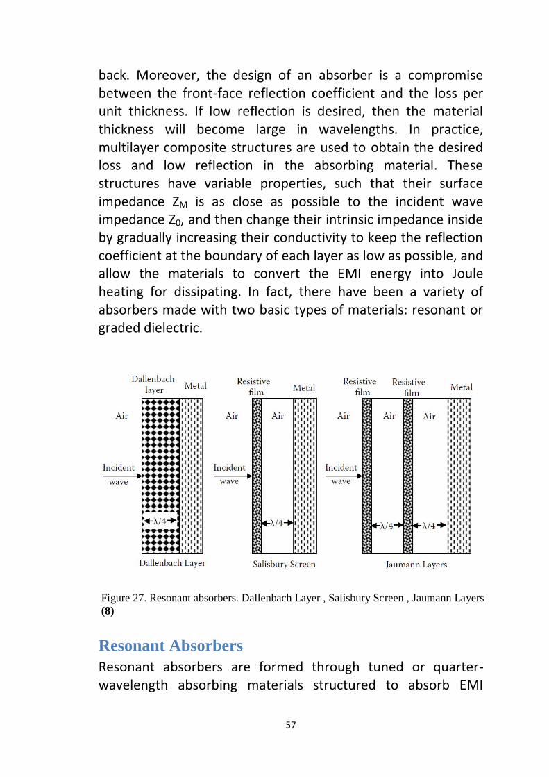
57
back. Moreover, the design of an absorber is a compromise between the front-face reflection coefficient and the loss per unit thickness. If low reflection is desired, then the material thickness will become large in wavelengths. In practice, multilayer composite structures are used to obtain the desired loss and low reflection in the absorbing material. These structures have variable properties, such that their surface impedance ZM is as close as possible to the incident wave impedance Z0, and then change their intrinsic impedance inside by gradually increasing their conductivity to keep the reflection coefficient at the boundary of each layer as low as possible, and allow the materials to convert the EMI energy into Joule heating for dissipating. In fact, there have been a variety of absorbers made with two basic types of materials: resonant or graded dielectric.
Resonant Absorbers
Resonant absorbers are formed through tuned or quarter-wavelength absorbing materials structured to absorb EMI
Figure 27. Resonant absorbers. Dallenbach Layer , Salisbury Screen , Jaumann Layers
(8)
58
energy at multiple frequencies. Resonant materials generally include Dallenbach layers, Salisbury screens, and Jaumann layers, as illustrated in Figure 27 from (8). In resonant absorbers, the material is thin and the impedance is not matched between incident and absorbing media so that not all EMI energy is absorbed. Therefore, both reflection and transmission of EMI wave will occur at the first interface. And then the reflected wave will undergo a phase reversal of π, while the transmitted wave travels through the absorbing medium and is reflected from a metal backing. This second reflection also results in a phase reversal of π before the wave propagates back to the incident medium. If the optical distance traveled by the transmitted wave is an even multiple of half wavelengths, then the two reflected waves will be out of phase and destructively interface. Moreover, if the magnitude of the two reflected wave is equal, then the total reflected intensity is zero. These resonant or tuned microwave absorbers usually exhibit high magnetic loss (permeability) or high dielectric loss (permittivity) with a quarter-wavelength of electrical thickness at the designed frequency. These absorbers require mounting on a ground plane or electrically conductive surface to achieve cancellation of the reflected EMI energy occurring at the front with the reflection occurring at the rear surface of the absorber. The phase of these two reflections is 180° or π apart due to the electrical thickness of a quarter wavelengths, resulting in cancellation of the two reflections.
Dallenbach Tuned Layer Absorbers
The Dallenbach layer is a layer of homogeneous lossy material placed on a conducting substrate. The thickness, permittivity, and permeability can be adjusted so that the reflectivity is minimized for a desired wavelength. The Dallenbach layer relies on destructive interference of the waves reflected from the first and second interfaces. To obtain a minimum reflectivity, the
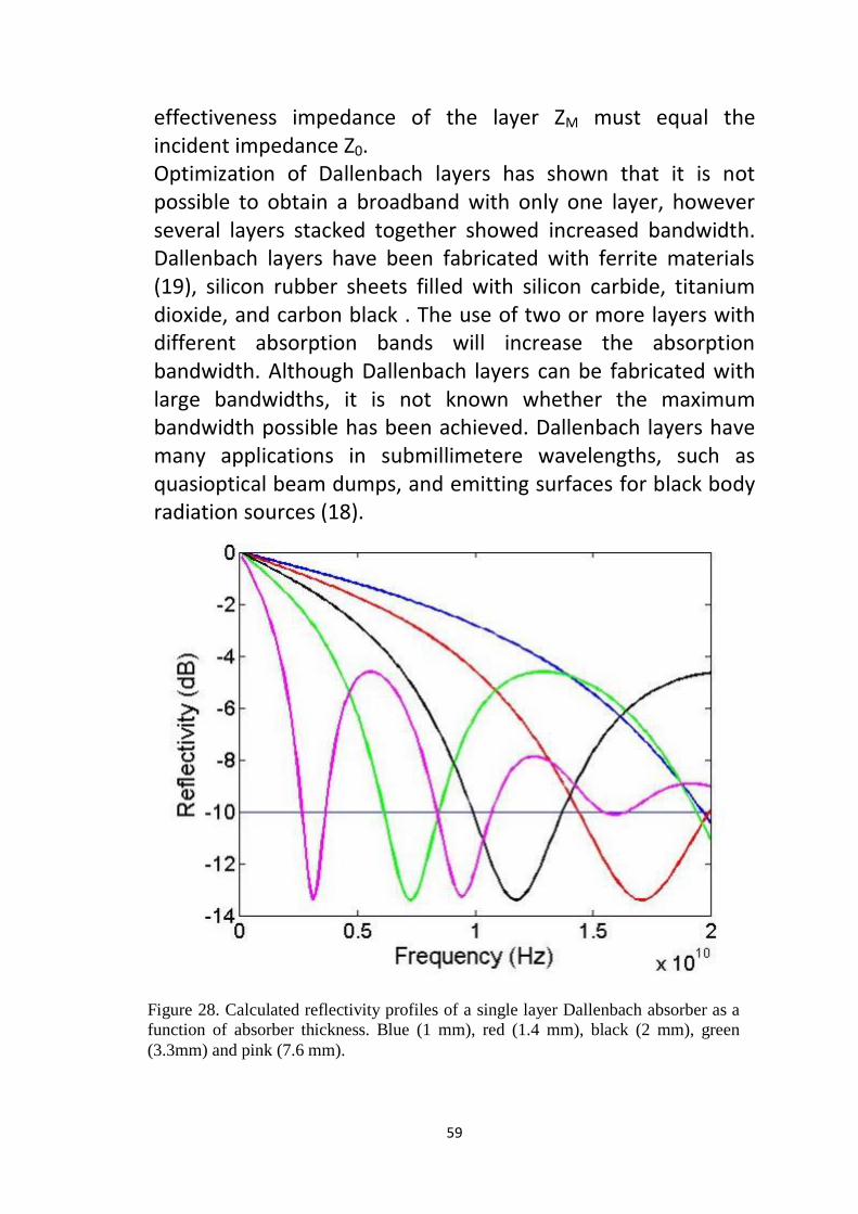
59
effectiveness impedance of the layer ZM must equal the incident impedance Z0. Optimization of Dallenbach layers has shown that it is not possible to obtain a broadband with only one layer, however several layers stacked together showed increased bandwidth. Dallenbach layers have been fabricated with ferrite materials (19), silicon rubber sheets filled with silicon carbide, titanium dioxide, and carbon black . The use of two or more layers with different absorption bands will increase the absorption bandwidth. Although Dallenbach layers can be fabricated with large bandwidths, it is not known whether the maximum bandwidth possible has been achieved. Dallenbach layers have many applications in submillimetere wavelengths, such as quasioptical beam dumps, and emitting surfaces for black body radiation sources (18).
Figure 28. Calculated reflectivity profiles of a single layer Dallenbach absorber as a
function of absorber thickness. Blue (1 mm), red (1.4 mm), black (2 mm), green
(3.3mm) and pink (7.6 mm).
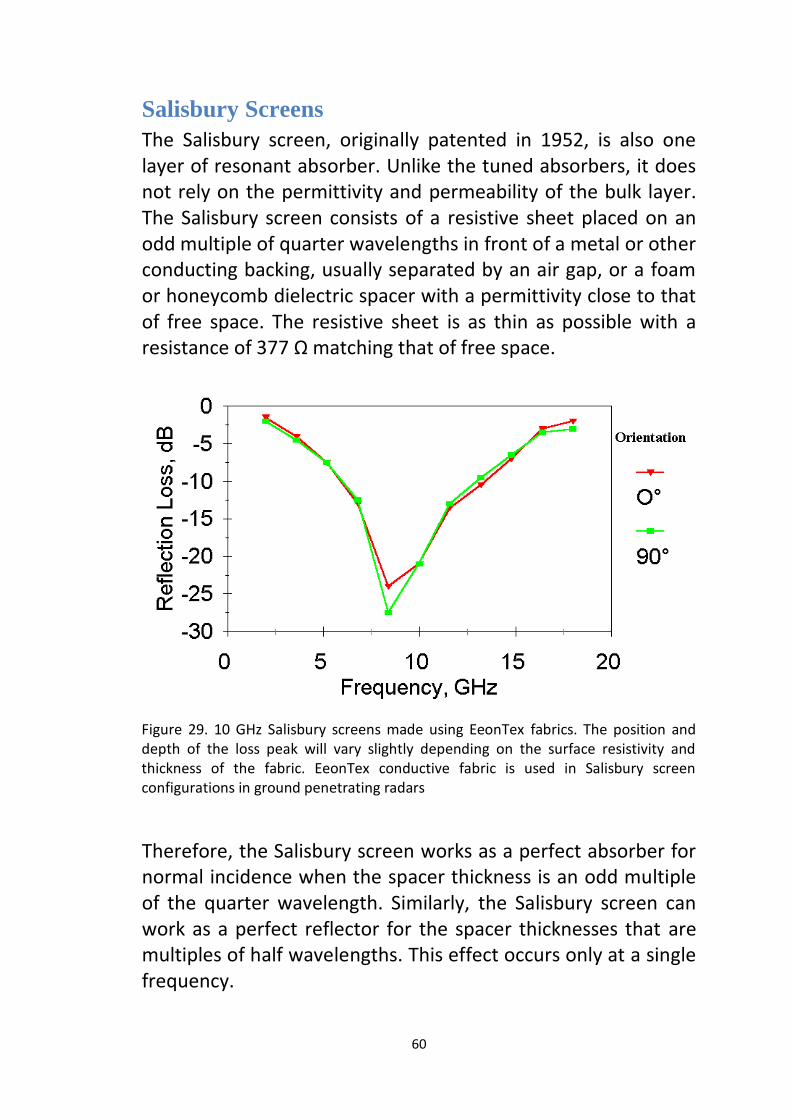
60
Salisbury Screens
The Salisbury screen, originally patented in 1952, is also one layer of resonant absorber. Unlike the tuned absorbers, it does not rely on the permittivity and permeability of the bulk layer. The Salisbury screen consists of a resistive sheet placed on an odd multiple of quarter wavelengths in front of a metal or other conducting backing, usually separated by an air gap, or a foam or honeycomb dielectric spacer with a permittivity close to that of free space. The resistive sheet is as thin as possible with a resistance of 377 Ω matching that of free space.
Therefore, the Salisbury screen works as a perfect absorber for normal incidence when the spacer thickness is an odd multiple of the quarter wavelength. Similarly, the Salisbury screen can work as a perfect reflector for the spacer thicknesses that are multiples of half wavelengths. This effect occurs only at a single frequency.
Figure 29. 10 GHz Salisbury screens made using EeonTex fabrics. The position and depth of the loss peak will vary slightly depending on the surface resistivity and thickness of the fabric. EeonTex conductive fabric is used in Salisbury screen configurations in ground penetrating radars
61
For this reason, Salisbury screens in their pure form have found little practical usage (18). Salisbury screens have been designed and fabricated in several ways. The initial patented structures were made of canvas on plywood frames with a colloidal graphite coating on the canvas. Conducting polymers and several other strategies have been used. The thickness of the optimal Salisbury screen can be calculated when the sheet resistance is equal to the impedance of free space Z0. The thickness of the resistivity sheet for optimum absorption has an inverse relationship to the sheet conductivity. The bandwidth of Salisbury screen can be maximized given the maximum acceptable reflectivity. The optimum sheet resistance was calculated to be 377 Ω for the lowest reflectivity, while the optimum resistance, Rs, for a given reflectivity limit is given by: Rs = Z0(1 – Γcutoff)/(1 + Γcutoff) where Γcutoff is the maximum acceptable reflectivity. Analytically, the bandwidth decreases with increasing permittivity of the spacing layer.
Jaumann Layers
Jaumann layers are a modification of the Salisbury screen that increase its bandwidth with multiple, thin, resistive layers separated with spacers on top of the metal backing . The cost of the increased bandwidth is the increased thickness of the absorber. The resistivity of the layers vary from high at the front face to low at the back. Resistive layers have been formulated using carbon powder (25 wt %) loaded phenol-formaldehyde, cellulose, or polyvinyl acetate binder with polyethylene foams as spacers. Silk screening resistive layers have produced better control of thickness and resistance. A six-layer Jaumann device is capable
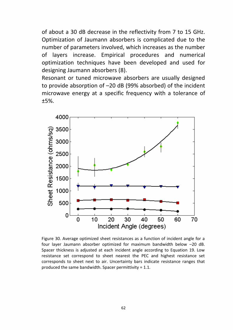
62
of about a 30 dB decrease in the reflectivity from 7 to 15 GHz. Optimization of Jaumann absorbers is complicated due to the number of parameters involved, which increases as the number of layers increase. Empirical procedures and numerical optimization techniques have been developed and used for designing Jaumann absorbers (8). Resonant or tuned microwave absorbers are usually designed to provide absorption of –20 dB (99% absorbed) of the incident microwave energy at a specific frequency with a tolerance of ±5%.
Figure 30. Average optimized sheet resistances as a function of incident angle for a four layer Jaumann absorber optimized for maximum bandwidth below –20 dB. Spacer thickness is adjusted at each incident angle according to Equation 19. Low resistance set correspond to sheet nearest the PEC and highest resistance set corresponds to sheet next to air. Uncertainty bars indicate resistance ranges that produced the same bandwidth. Spacer permittivity = 1.1.
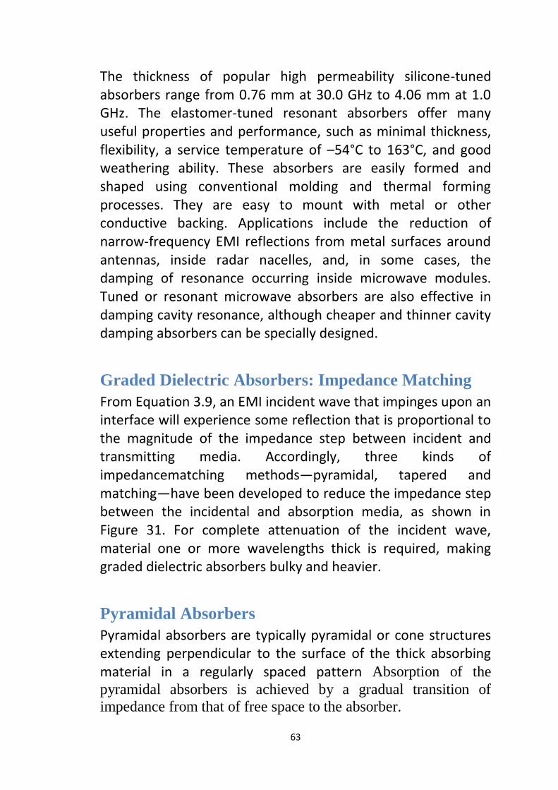
63
The thickness of popular high permeability silicone-tuned absorbers range from 0.76 mm at 30.0 GHz to 4.06 mm at 1.0 GHz. The elastomer-tuned resonant absorbers offer many useful properties and performance, such as minimal thickness, flexibility, a service temperature of –54°C to 163°C, and good weathering ability. These absorbers are easily formed and shaped using conventional molding and thermal forming processes. They are easy to mount with metal or other conductive backing. Applications include the reduction of narrow-frequency EMI reflections from metal surfaces around antennas, inside radar nacelles, and, in some cases, the damping of resonance occurring inside microwave modules. Tuned or resonant microwave absorbers are also effective in damping cavity resonance, although cheaper and thinner cavity damping absorbers can be specially designed.
Graded Dielectric Absorbers: Impedance Matching
From Equation 3.9, an EMI incident wave that impinges upon an interface will experience some reflection that is proportional to the magnitude of the impedance step between incident and transmitting media. Accordingly, three kinds of impedancematching methods—pyramidal, tapered and matching—have been developed to reduce the impedance step between the incidental and absorption media, as shown in Figure 31. For complete attenuation of the incident wave, material one or more wavelengths thick is required, making graded dielectric absorbers bulky and heavier.
Pyramidal Absorbers
Pyramidal absorbers are typically pyramidal or cone structures extending perpendicular to the surface of the thick absorbing material in a regularly spaced pattern Absorption of the
pyramidal absorbers is achieved by a gradual transition of
impedance from that of free space to the absorber.
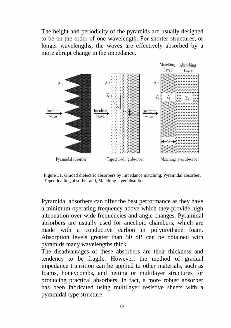
64
The height and periodicity of the pyramids are usually designed
to be on the order of one wavelength. For shorter structures, or
longer wavelengths, the waves are effectively absorbed by a
more abrupt change in the impedance.
Pyramidal absorbers can offer the best performance as they have
a minimum operating frequency above which they provide high
attenuation over wide frequencies and angle changes. Pyramidal
absorbers are usually used for anechoic chambers, which are
made with a conductive carbon in polyurethane foam.
Absorption levels greater than 50 dB can be obtained with
pyramids many wavelengths thick.
The disadvantages of these absorbers are their thickness and
tendency to be fragile. However, the method of gradual
impedance transition can be applied to other materials, such as
foams, honeycombs, and netting or multilayer structures for
producing practical absorbers. In fact, a more robust absorber
has been fabricated using multilayer resistive sheets with a
pyramidal type structure.
Figure 31. Graded dielectric absorbers by impedance matching. Pyramidal absorber,
Taped loading absorber and, Matching layer absorber
65
Tapered Loading Absorbers
The tapered loading absorber is typically a slab made with a
mixture of low loss material and lossy material. The lossy
component is homogeneously dispersed parallel to the incident
surface, with a gradient perpendicular to the surface and
increasing into the slab . One type of tapered loading material
consists of open-cell foam or plastic net, dipped or sprayed with
lossy material from one side, or allowed to drain and dry (8).
It is hard to reproducibly fabricate a gradient in this manner.
Another type is composed of homogeneous layers with increased
loading of lossy material in the direction of EMI propagation.
The advantage of these materials is that they are thinner
than the pyramidal absorbers.
Figure 32. This class of absorber has been developed specifically for radiated emission test chambers. It is also useful in other applications such as radiated susceptibility. Give good reflectivity performance in the critical low-frequency range (from 30 MHz up) of EMC/EMI test chambers. However, the absorber still performs more than adequately at higher frequencies up to at least 18 GHz.
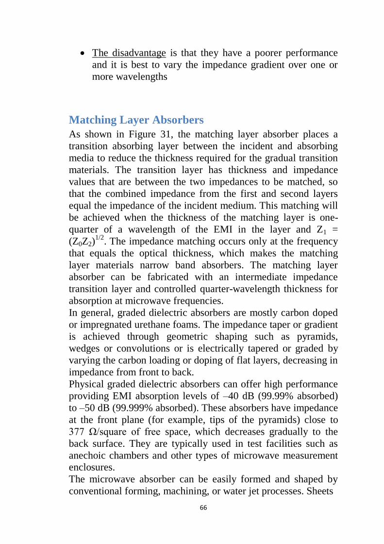
66
The disadvantage is that they have a poorer performance
and it is best to vary the impedance gradient over one or
more wavelengths
Matching Layer Absorbers
As shown in Figure 31, the matching layer absorber places a
transition absorbing layer between the incident and absorbing
media to reduce the thickness required for the gradual transition
materials. The transition layer has thickness and impedance
values that are between the two impedances to be matched, so
that the combined impedance from the first and second layers
equal the impedance of the incident medium. This matching will
be achieved when the thickness of the matching layer is one-
quarter of a wavelength of the EMI in the layer and Z1 =
(Z0Z2)1/2
. The impedance matching occurs only at the frequency
that equals the optical thickness, which makes the matching
layer materials narrow band absorbers. The matching layer
absorber can be fabricated with an intermediate impedance
transition layer and controlled quarter-wavelength thickness for
absorption at microwave frequencies.
In general, graded dielectric absorbers are mostly carbon doped
or impregnated urethane foams. The impedance taper or gradient
is achieved through geometric shaping such as pyramids,
wedges or convolutions or is electrically tapered or graded by
varying the carbon loading or doping of flat layers, decreasing in
impedance from front to back.
Physical graded dielectric absorbers can offer high performance
providing EMI absorption levels of –40 dB (99.99% absorbed)
to –50 dB (99.999% absorbed). These absorbers have impedance
at the front plane (for example, tips of the pyramids) close to
377 Ω/square of free space, which decreases gradually to the
back surface. They are typically used in test facilities such as
anechoic chambers and other types of microwave measurement
enclosures.
The microwave absorber can be easily formed and shaped by
conventional forming, machining, or water jet processes. Sheets
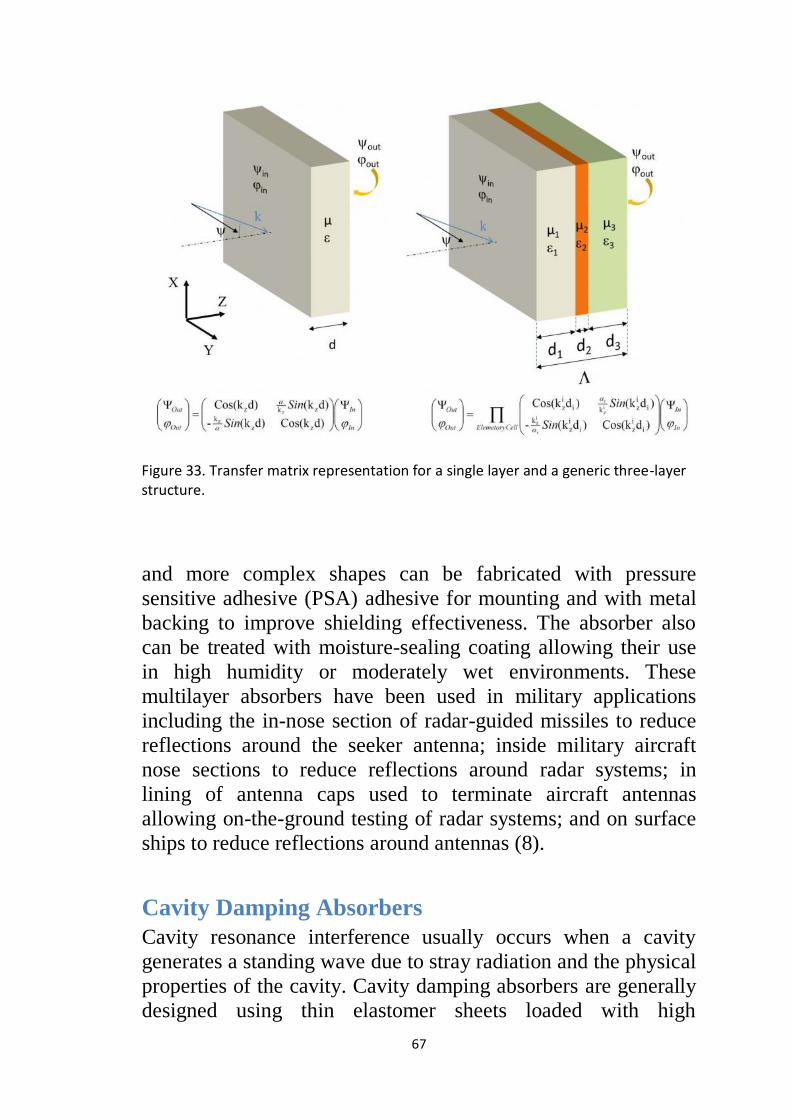
67
and more complex shapes can be fabricated with pressure
sensitive adhesive (PSA) adhesive for mounting and with metal
backing to improve shielding effectiveness. The absorber also
can be treated with moisture-sealing coating allowing their use
in high humidity or moderately wet environments. These
multilayer absorbers have been used in military applications
including the in-nose section of radar-guided missiles to reduce
reflections around the seeker antenna; inside military aircraft
nose sections to reduce reflections around radar systems; in
lining of antenna caps used to terminate aircraft antennas
allowing on-the-ground testing of radar systems; and on surface
ships to reduce reflections around antennas (8).
Cavity Damping Absorbers
Cavity resonance interference usually occurs when a cavity
generates a standing wave due to stray radiation and the physical
properties of the cavity. Cavity damping absorbers are generally
designed using thin elastomer sheets loaded with high
Figure 33. Transfer matrix representation for a single layer and a generic three-layer structure.
68
permeability materials providing broad frequency magnetic loss
properties. Other absorbers, such as resonant or tuned absorbers,
may also be good for cavity damping but may not be the best
selection based on cost and weight. High-permeability cavity
damping absorbers can be formed and shaped using a
conventional forming tool, razor blade, water jet, or laser
cutting, ranging in thickness from 0.25 mm to 1.0 mm. Silicone
is commonly used for the binder material due to its flexibility,
service temperature of –54°C to 163°C, power handling of 0.2
W/cm2, low outgassing, and availability with a high performance
peel-and-stick pressure-sensitive adhesive (8).
Figure 34. In the above CLIC accelerating cell, \citegrudiev2009possible the four radial rectangular waveguides (terminated by electromagnetic absorbers) strongly
damp HOMs; the cutoff frequency of each waveguide is slightly above the
accelerating mode frequency and well below the lowest dipole frequency.
69
Cavity resonance problems are frequently met when the circuit
board is integrated with the shielded cavity or chassis, due partly
to increased circuit function, and reduction in the physical size
of microwave circuit board in metallic shielding housings.
Microwave cavities have certain frequencies that oscillate. The
interference energy can be attenuated when lossy magnetic or
dielectric materials are installed into the cavity. Specific cavity
damping can be theoretically selected through complex
resonance modeling. Optimized magnetic loss materials are
frequently utilized for reducing microwave cavity resonance
because these materials, like iron-loaded silicone, offer thin,
nonconductive characteristics without the risk of shorting the
circuit board. Comparatively, dielectric loss materials, such as
latex-coated elastomer foam structures, are usually thicker but
cost less than magnetic loss materials.
However, if environmental conditions allow and if the thickness
can be tolerated, this foam structure can be a viable option. Both
dielectric loss and magnetic loss materials are effective for
reducing cavity resonance (14).
Most cavity damping absorber materials are applied to the cover
of the microwave module. In multiple-cavity modules, twenty to
fifty cavities can be in a module. Some cavities have no
microwave circuitry, while others with house microwave
circuitry require cavity damping absorbers. A mold-in-place
process can be used to apply the cavity damping absorber to the
resonant cavities of multiple-cavity housing.
Anechoic Chambers
The anechoic chamber is an radio frequency (RF)-shielded room
mainly consisting of an antenna system and RF absorber
materials installed on the four walls, ceiling, and possibly the
floor. The design of an anechoic chamber is basically established
for performing EMC measurements according to a variety of
different published EMC standards, involving many different
fields of application, such as consumer electronics, automotive,
aerospace, military, medical, and telecommunications. Anechoic
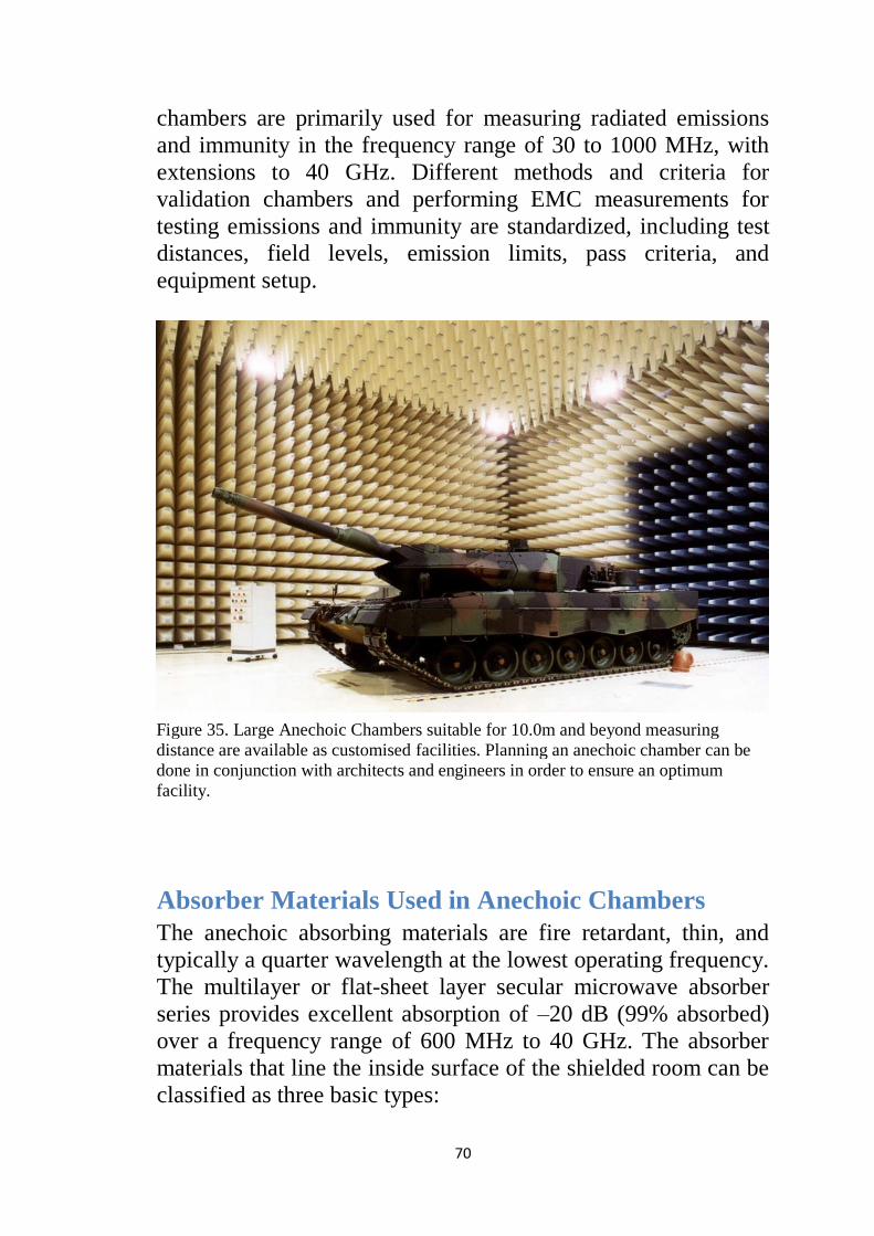
70
chambers are primarily used for measuring radiated emissions
and immunity in the frequency range of 30 to 1000 MHz, with
extensions to 40 GHz. Different methods and criteria for
validation chambers and performing EMC measurements for
testing emissions and immunity are standardized, including test
distances, field levels, emission limits, pass criteria, and
equipment setup.
Absorber Materials Used in Anechoic Chambers
The anechoic absorbing materials are fire retardant, thin, and
typically a quarter wavelength at the lowest operating frequency.
The multilayer or flat-sheet layer secular microwave absorber
series provides excellent absorption of –20 dB (99% absorbed)
over a frequency range of 600 MHz to 40 GHz. The absorber
materials that line the inside surface of the shielded room can be
classified as three basic types:
Figure 35. Large Anechoic Chambers suitable for 10.0m and beyond measuring
distance are available as customised facilities. Planning an anechoic chamber can be
done in conjunction with architects and engineers in order to ensure an optimum
facility.
71
1. Electric loss pyramidal absorber. This is the preferred
technology for high frequencies with a range of 100 MHz
to 18 GHz. The losses are provided by carbon loading of a
pyramid structure.
2. Magnetic loss ferrite tile. This is the preferred technology
for low frequencies with a range of 30 to 1000 MHz.
Ferrite tile, 5 to 6 mm, provides the magnetic losses, and is
used in combination with hybrid foam to form a united
absorber. The disadvantage of this material is that it is
heavy and cannot be used for high frequencies.
3. Electric and magnetic loss hybrid absorber. This is
preferred technology for broadband EMC testing generally
with a frequency range of 30 MHz to 18 GHz. Specially
formulated hybrid pyramid foam has good matching with
ferrite tile at the bottom. However, its performance is not
as good as electric loss pyramid of equal size at high
frequencies.
Anechoic chambers are generally different upon their
application and can be divided into the following groups:
a) partially lined room—the surfaces are not fully covered
with absorbers;
b) semi-anechoic room—the walls and ceiling are covered
with absorbers whereas the floor is a metal reflecting
ground plane; and
c) fully anechoic room—all surfaces are covered with
absorbers. The most common type of chamber will be a
compact or full 3 m type.
The compact chamber offers the advantage of being able to fit
into the majority of buildings due to their limited height of 3 m.
The full 3 m and larger chambers will be part of a dedicated
building purposely built in many cases to house the chamber. In
parallel with the transient nature of some markets like telecoms,
most of these chambers offer the flexibility of being removable
or modified to a different size if the requirements of the testing
72
change or the company move to a different location. The life
cycle of the products has increased together with the quality of
some of the key maintenance items like shielded doors. Types of
measurements conducted in these anechoic chambers include
attenuation measurements, radar cross-section, EMI emissions,
susceptibility and compatibility, and target simulation.
Metamaterial Shielding
Metamaterials Introduction
Artificial materials are composite structures consisting of
inclusions periodically embedded in a host matrix. When the
size of the inclusions and the spatial periods are small compared
with the wavelength of the EM field generated by a source, such
artificial materials can be homogenized; that is, they can be
described as homogeneous materials with effective constitutive
parameters that depend on the geometrical and physical
properties of the inclusions and of the host medium, and on
how the inclusions are placed in the host matrix. If the
homogenized artificial materials present EM properties that
conventional materials do not possess, they are also called
metamaterials. Other artificial materials based on periodic
structures, such as electromagnetic-band-gap (EBG) structured
materials and complex surfaces (e.g., high-impedance ground
planes and artificial magnetic conductors), involve distances and
dimensions of the order of the wavelength or more; they are
strongly inhomogeneous and need to be described by the
periodicmedia formalism.
The most popular class of metamaterials includes structures for
which the values of the (effective) permittivity and permeability
are simultaneously negative, as considered in. A material having
this property can be used to obtain a series of surprising effects,
such as backward-wave propagation in the material, a negative
index of refraction, or a reversed Doppler effect. The most
famous application suggests the possibility of fabricating a
superlens providing spatial resolution beyond the diffraction
limit. Up to now there is not a common terminology used to
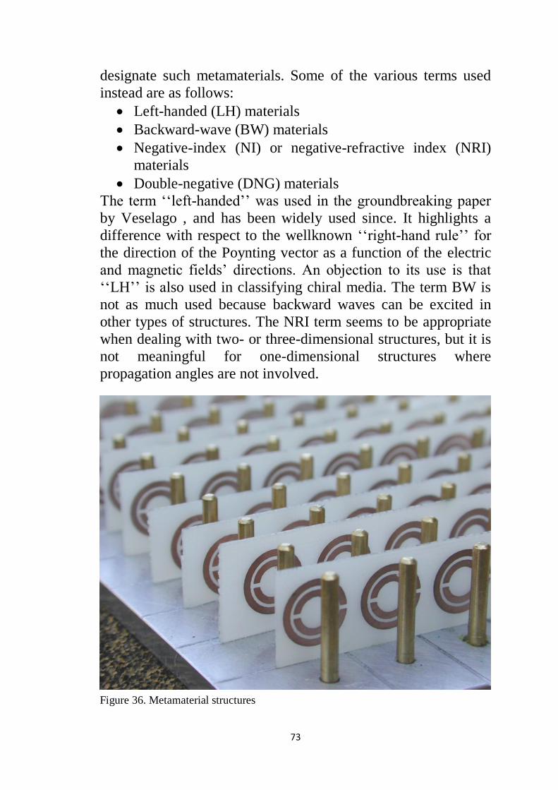
73
designate such metamaterials. Some of the various terms used
instead are as follows:
Left-handed (LH) materials
Backward-wave (BW) materials
Negative-index (NI) or negative-refractive index (NRI)
materials
Double-negative (DNG) materials
The term ‘‘left-handed’’ was used in the groundbreaking paper
by Veselago , and has been widely used since. It highlights a
difference with respect to the wellknown ‘‘right-hand rule’’ for
the direction of the Poynting vector as a function of the electric
and magnetic fields’ directions. An objection to its use is that
‘‘LH’’ is also used in classifying chiral media. The term BW is
not as much used because backward waves can be excited in
other types of structures. The NRI term seems to be appropriate
when dealing with two- or three-dimensional structures, but it is
not meaningful for one-dimensional structures where
propagation angles are not involved.
Figure 36. Metamaterial structures
74
The terms above represent in each case a property resulting from
a wave propagating within the metamaterial structure. The term
DNG is instead a consequence of the properties of the (effective)
constitutive parameters of the material itself (whose permittivity
and permeability have both negative values). For ordinary
materials these values are both positive, with the noticeable
exception represented by ferrimagnetic materials (although
usually negative values of the permeability occur in a very
narrow band) and plasma. Moreover the reason behind the
acronym DNG can be used to define double-positive (DPS) or
single-negative (SNG) materials, as only-ε-negative (ENG) and
only-μ-negative (MNG) (20).
Many metamaterial structures have been designed and fabricated
over the last few years, and their performances have been
verified by measurements. However, this topic is still relatively
new and in so rapid development that any attempt at giving
limits of applicability, quantitative orders of magnitude of the
characteristic parameters, and so forth, is prone to be surpassed
by new discoveries, technologies, or applications.
Shielding With Metamaterial
The issue of invisibility by means of metamaterial coatings has
continued to be studied, and a large number of papers are being
published on this topic . Invisibility means that an object is made
nearly transparent to an external observer; that is, its scattering
cross section is dramatically reduced, at least in a narrow
frequency range. Much effort is directed toward the design of
metamaterial structures that operate as cloaks of invisibility in
the microwave and in the optical frequency range. Different
ideas and techniques are being tried. On one hand, the use of
anisotropic and/or inhomogeneous metamaterials has seemed to
allow for a control of field distribution (21). That is to roughly
say, the EM field is swept around the coated scatterer, and it
appears as if it had passed there through an empty volume of
space; experimental results are already available. On the other
hand, similar effects have been theoretically predicted using
isotropic and homogeneous metamaterials as coatings (21). In
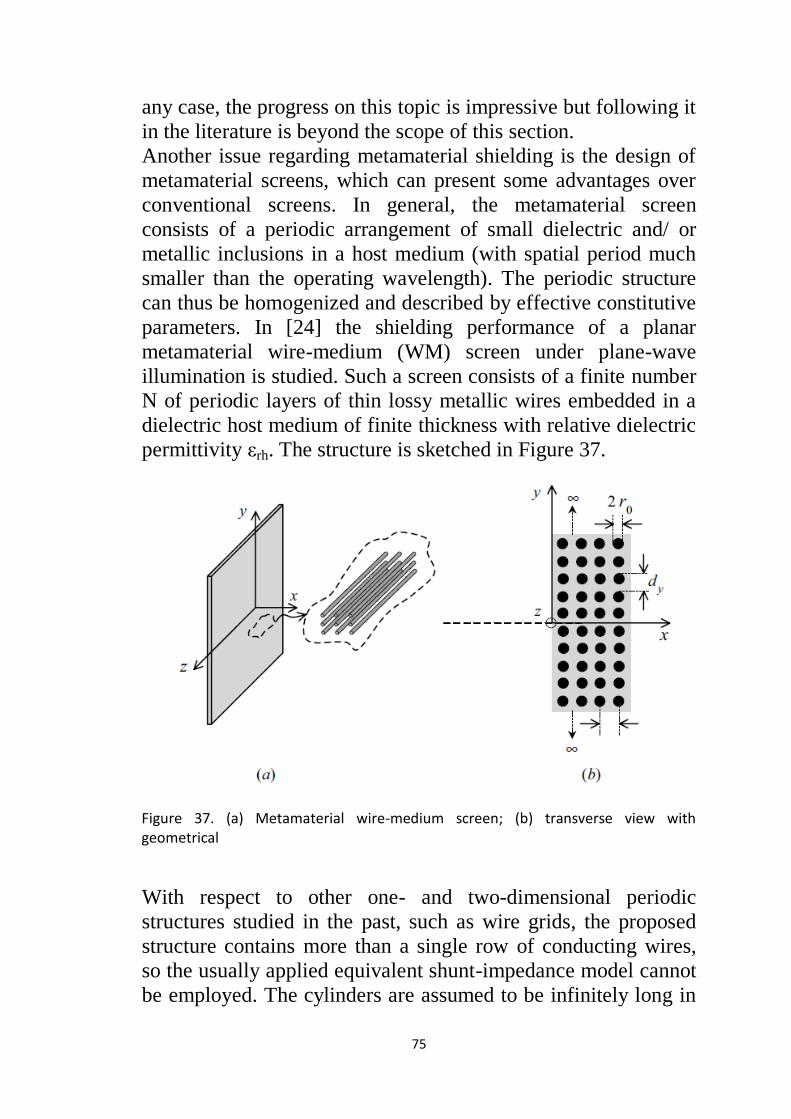
75
any case, the progress on this topic is impressive but following it
in the literature is beyond the scope of this section.
Another issue regarding metamaterial shielding is the design of
metamaterial screens, which can present some advantages over
conventional screens. In general, the metamaterial screen
consists of a periodic arrangement of small dielectric and/ or
metallic inclusions in a host medium (with spatial period much
smaller than the operating wavelength). The periodic structure
can thus be homogenized and described by effective constitutive
parameters. In [24] the shielding performance of a planar
metamaterial wire-medium (WM) screen under plane-wave
illumination is studied. Such a screen consists of a finite number
N of periodic layers of thin lossy metallic wires embedded in a
dielectric host medium of finite thickness with relative dielectric
permittivity εrh. The structure is sketched in Figure 37.
With respect to other one- and two-dimensional periodic
structures studied in the past, such as wire grids, the proposed
structure contains more than a single row of conducting wires,
so the usually applied equivalent shunt-impedance model cannot
be employed. The cylinders are assumed to be infinitely long in
Figure 37. (a) Metamaterial wire-medium screen; (b) transverse view with geometrical
76
the z direction; the spatial period along the y direction is dy, and
the diameter of the cylinders is 2r0. The distance dx between
each row of cylinders is assumed to be equal to the spatial
period, meaning dx = dy = d. The main assumption that has to be
made in order to correctly perform a homogenization of the
periodic structure consists in considering the spatial period d
suitably smaller than the operating wavelength λ0. In such a case
it can be shown that the periodic structure can be represented
from the effective-medium-theory viewpoint as a homogeneous
nonmagnetic medium characterized by an effective diagonal
permittivity tensor.
The two elements of such a tensor corresponding to directions
orthogonal to the wires (εxx and εyy) are simply equal to the
dielectric permittivity of the host medium, whereas the
remaining element εzz is characterized by both temporal and
spatial dispersion.
However, the propagation of EM waves with an electric field
polarized along the wire direction z is unaffected by the
anisotropy and the spatial dispersion. The medium can thus be
represented by a simple scalar frequency-dependent
permittivity, whose behavior resembles that of a cold
nonmagnetized collisionless plasma:
where fp/( εrh )
0.5 is the plasma frequency at which the effective
permittivity of the wire medium is equal to zero. The frequency
fp mainly depends on the geometrical parameters of the
structure. In the limit of small radius (i.e., r0 << d), there results
Finally, in the homogenization process a finite thickness heff has
to be associated to the homogeneous slab equivalent to the
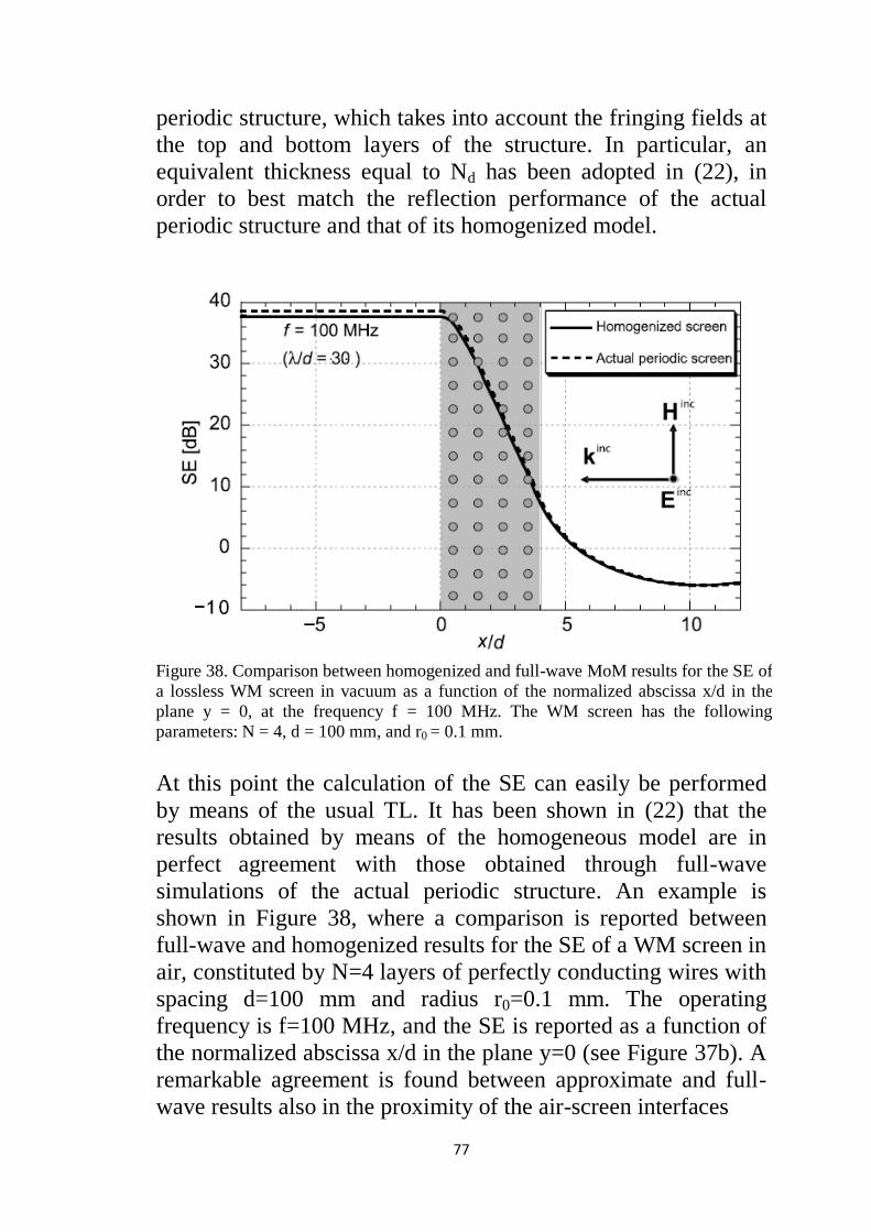
77
periodic structure, which takes into account the fringing fields at
the top and bottom layers of the structure. In particular, an
equivalent thickness equal to Nd has been adopted in (22), in
order to best match the reflection performance of the actual
periodic structure and that of its homogenized model.
At this point the calculation of the SE can easily be performed
by means of the usual TL. It has been shown in (22) that the
results obtained by means of the homogeneous model are in
perfect agreement with those obtained through full-wave
simulations of the actual periodic structure. An example is
shown in Figure 38, where a comparison is reported between
full-wave and homogenized results for the SE of a WM screen in
air, constituted by N=4 layers of perfectly conducting wires with
spacing d=100 mm and radius r0=0.1 mm. The operating
frequency is f=100 MHz, and the SE is reported as a function of
the normalized abscissa x/d in the plane y=0 (see Figure 37b). A
remarkable agreement is found between approximate and full-
wave results also in the proximity of the air-screen interfaces
Figure 38. Comparison between homogenized and full-wave MoM results for the SE of
a lossless WM screen in vacuum as a function of the normalized abscissa x/d in the
plane y = 0, at the frequency f = 100 MHz. The WM screen has the following
parameters: N = 4, d = 100 mm, and r0 = 0.1 mm.
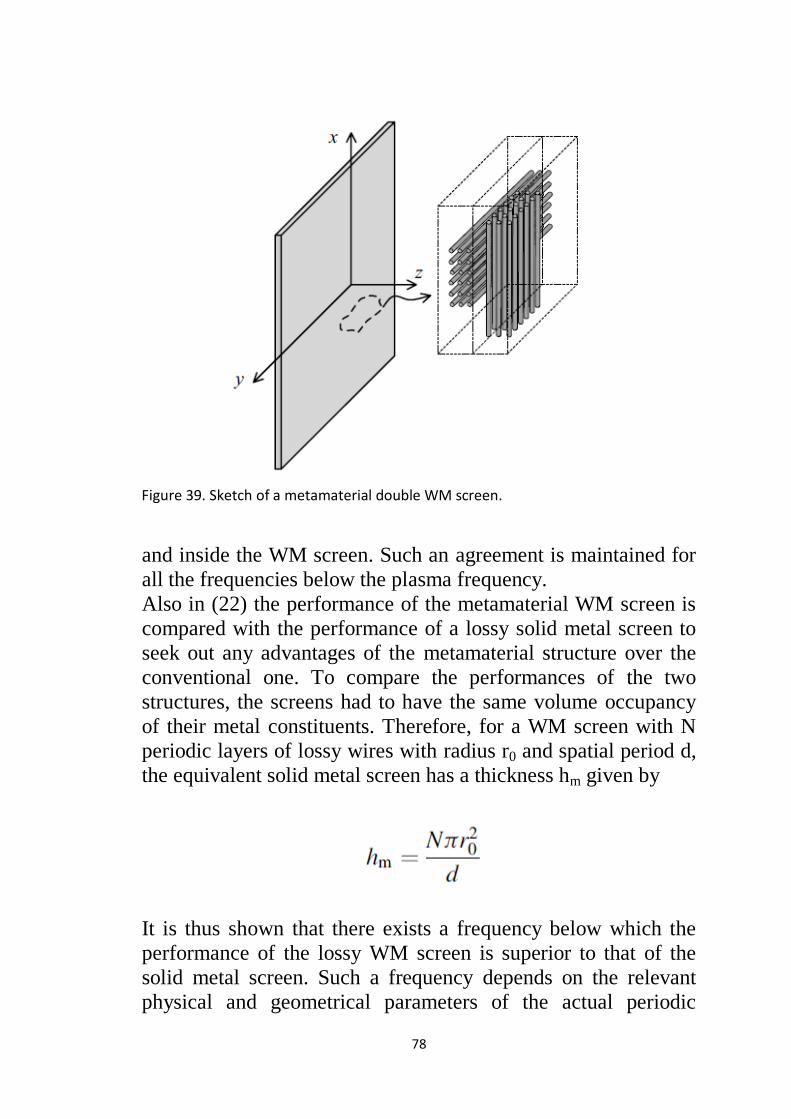
78
and inside the WM screen. Such an agreement is maintained for
all the frequencies below the plasma frequency.
Also in (22) the performance of the metamaterial WM screen is
compared with the performance of a lossy solid metal screen to
seek out any advantages of the metamaterial structure over the
conventional one. To compare the performances of the two
structures, the screens had to have the same volume occupancy
of their metal constituents. Therefore, for a WM screen with N
periodic layers of lossy wires with radius r0 and spatial period d,
the equivalent solid metal screen has a thickness hm given by
It is thus shown that there exists a frequency below which the
performance of the lossy WM screen is superior to that of the
solid metal screen. Such a frequency depends on the relevant
physical and geometrical parameters of the actual periodic
Figure 39. Sketch of a metamaterial double WM screen.
79
structure, and it can be estimated in planning an effective design
for the WM screen. Furthermore a dramatically different
behavior of the SE is observed as a function of frequency in the
solid and WM screens. In particular, while the SE monotonically
increases with the frequency for the solid screen, it first
increases and then decreases in the WM case, thus showing a
possibly desirable selective property. It is speculated that, by
suitably modifying the internal geometry of the metamaterial,
such frequency selectivity can be controlled and possibly further
enhanced.
On the other hand, the considered WM screen was observed to
be completely transparent to waves with the electric field
orthogonal to the wires. For this reason, to enhance its
effectiveness against arbitrarily polarized plane waves, a second
WM screen was introduced in (22), with wires orthogonal to
those of the first screen (as shown in Figure 39), and this setup
was studied under normal incidence. The analysis of single- or
double-layer WM screens illuminated by arbitrarily polarized
plane waves at oblique incidence nevertheless requires a more
sophisticated description of the equivalent homogenized
metamaterial and a considerably more involved transmission-
line model. So work is still in progress, as well as an analysis of
other planar metamaterial screens based on different inclusions.
80
References
1. Ravaioli, Fawwaz T. Ulaby, Eric Michielssen, Umberto (2010).
Fundamentals of applied electromagnetics (6th ed.). Boston: Prentice
Hall.
2. http://en.wikipedia.org/wiki/Electromagnetism#cite_note-1.
3. J. C. Maxwell, A Treatise on Electricity and Magnetism, Dover, New
York, 1954.
4. Bakshi, U. A. and Godse, A. P. (2009). Basic Electronics Engineering.
Technical Publications.
5. John C. Pfeiffer, Principles of Electrical Grounding, 2001.
6.http://www.wisegeek.org/what-is-electromagnetic-
shielding.htm#didyouknowout.
7. http://www.4emi.com/shielding-actually-works/.
8. Xingcun Colin Tong, Advanced Materials and Design for
Electromagnetic Interference Shielding, 2009 by Taylor & Francis Group,
LLC, CRC Press is an imprint of Taylor & Francis Group, an Informa
business, International Standard Book Number-13: 978-1-4200-73.
9. P. S. Neelakanta. Handbook of Electromagnetic Materials: Monolithic
and Composite Versions and their Applications. Boca Raton: CRC Press,
1995.
10. Terence Rybak, Mark Steffka, Automotive Electromagnetic
Compatibility (Emc) , Kluwer Academic Publishers, New York, Boston,
Dordrecht, London, Moscow, 2004, Ebook Isbn: 1-4020-7783-1, Print
Isbn: 1-4020-7713-0.
11. http://en.wikipedia.org/wiki/Skin_effect.
12. Leland H. Hemming, Architectural Electromagnetic Shielding
Handbook A Design and Specification Guide, IEEE PRESS, 445 Hoes
Lane, PO Box 1331, Piscataway, NJ 08855-1331.
81
13. Sophocles J. Orfanidis, Electromagnetic Waves and Antennas, is a
registered trademark of The MathWorks, Inc.
14. Dixon, P. 2004, May. Dampening cavity resonance using absorber
material. RF Design, pp. 16–20. http://rfdesign.com/mag/0405rfdf1.pdf.
15. http://www.sony.net/Products/SC-HP/cx_news/vol25/pdf/emcstw.pdf,
Sony. 2008. Sony’s electromagnetic wave absorber reduces EMC and
SAR problem.
16. Gear, J. T. 2004, August. Microwave absorbers manage military
electronics RF interference. RF Design, pp. 6–9.
http://rfdesign.com/mag/08deff1.pdf.
17. Chatterton, P. A., and M. A. Houlden. 1992. EMC Electromagnetic
Theory to Practical Design. Hoboken, NJ: John Wiley & Sons.
18. Saville, P. 2005. A review of optimisation techniques for layered
radar absorbing materials(Technical memorandum 2005-003). Defence
R&D Canada. http://pubs.drdc.gc.ca/ PDFS/unc57/p523186.pdf.
19. Mayer, F. 1999. High frequency broadband absorption structures. US
Patent 5,872,534.
20. Salvatore Celozzi, Rodolfo Araneo , Giampiero Lovat ,
Electromagnetic Shielding, Wiley Series In Microwave And Optical
Engineering, 2008, ISBN 978-0-470-05536-6.
21. J. B. Pendry, D. Schurig, and D. R. Smith.‘‘Controlling
electromagnetic fields.’’ Science, vol. 312, pp. 1780–1782, Jun. 2006.
22. G. Lovat, P. Burghignoli, and S. Celozzi.‘‘Shielding properties of a
metamaterial wire-medium screen.’’ IEEE Trans. Electromagn. Compat.,
vol. 50, no. 1, pp. 80–88, Feb. 2008.
23. Henry W. Ott, Electromagnetic Compatibility Engineering , 2009 by
John Wiley & Sons, Inc., ISBN 978-0-470-18930-6.


![downloads.spj.sciencemag.org · Web view[4]X. Shui, and D. Chung, "Nickel filament polymer-matrix composites with low surface impedance and high electromagnetic interference shielding](https://img.pdfslide.us/doc/110x75/613de84d2809574f586e4347/web-view-4x-shui-and-d-chung-nickel-filament-polymer-matrix-composites.jpg)