Embed Size (px)
Citation preview

1
Introduction
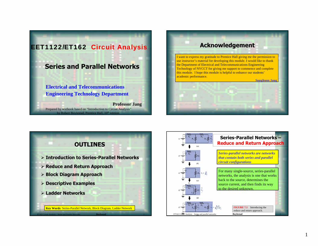
EET1122/ET162 Circuit Analysis
Electrical and Telecommunications Engineering Technology Department
Professor JangPrepared by textbook based on “Introduction to Circuit Analysis”
by Robert Boylestad, Prentice Hall, 10th edition.
AcknowledgementAcknowledgement
I want to express my gratitude to Prentice Hall giving me the permission to use instructor’s material for developing this module. I would like to thank the Department of Electrical and Telecommunications Engineering Technology of NYCCT for giving me support to commence and complete this module. I hope this module is helpful to enhance our students’ academic performance.
Sunghoon Jang
OUTLINESOUTLINESIntroduction to Electrical Engineering
A Brief History
Units of Measurement
Systems of Units
Operation of a Scientific Calculator
Significant Figures
ET162 Circuit Analysis – Introduction Boylestad 2
Key Words: Electrical Engineering, Units, Powers, Calculator
Introduction – The Electrical/Electronics Engineering
The growing sensitivity to the technologies on Wall Street is clear evidence that the electrical/electronics industry is one that will have a sweeping impact on future development in a wide range of areas that affect our life style, general health, and capabilities.
• Semiconductor Device
• Analog & Digital Signal Processing
• Telecommunications
• Biomedical Engineering
• Fiber Optics & Opto-Electronics
• Integrated Circuit (IC)
Figure 1.1 Computer chip on finger. (Courtesy of Intel Corp.)
ET162 Circuit Analysis – Introduction Boylestad 3
2
Introduction – A Brief History
FIGURE 1.2FIGURE 1.2 Time charts: (a) Time charts: (a) longlong--range; (b) expandedrange; (b) expanded..
ET162 Circuit Analysis – Introduction Boylestad 4
Units of Measurement
The numerical value substituted into an equation must haveThe unit of measurement specified by the equation
1 mi = 5280 ft4000 ft = 0.7576 mi1 min = 0.0167 h
Examples
hmihmi
tdv /73.45
0167.07576.0 ===
ET162 Circuit Analysis – Introduction Boylestad 5
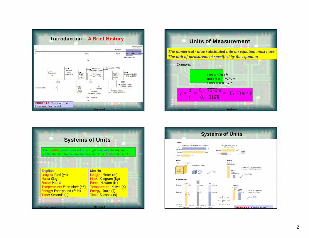
Systems of Units
EnglishLength: Yard (yd)Mass: SlugForce: PoundTemperature: Fahrenheit (°F)Energy: Foot-pound (ft-lb)Time: Seconds (s)
MetricLength: Meter (m)Mass: Kilogram (kg)Force: Newton (N)Temperature: Kelvin (K)Energy: Joule (J)Time: Seconds (s)
The English system is based on a single standard, the metric is subdivided into two interrelated standards: the MKS and the CGS.
ET162 Circuit Analysis – Introduction Boylestad 6
Systems of Units
FIGURE 1.3FIGURE 1.3 Comparison of Comparison of
3
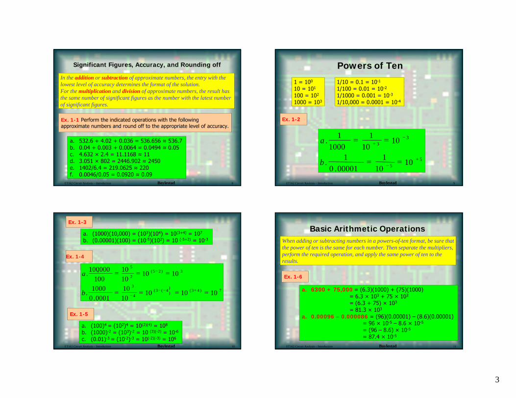
Significant Figures, Accuracy, and Rounding off
Ex. 1-1 Perform the indicated operations with the following approximate numbers and round off to the appropriate level of accuracy.
a. 532.6 + 4.02 + 0.036 = 536.656 ≈ 536.7b. 0.04 + 0.003 + 0.0064 = 0.0494 ≈ 0.05c. 4.632 × 2.4 = 11.1168 ≈ 11d. 3.051 × 802 = 2446.902 ≈ 2450e. 1402/6.4 = 219.0625 ≈ 220f. 0.0046/0.05 = 0.0920 ≈ 0.09
In the addition or subtraction of approximate numbers, the entry with the lowest level of accuracy determines the format of the solution.For the multiplication and division of approximate numbers, the result has the same number of significant figures as the number with the latest number of significant figures.
ET162 Circuit Analysis – Introduction Boylestad 8
Powers of Ten
1 = 100
10 = 101
100 = 102
1000 = 103
1/10 = 0.1 = 10-1
1/100 = 0.01 = 10-2
1/1000 = 0.001 = 10-3
1/10,000 = 0.0001 = 10-4
ET162 Circuit Analysis – Introduction Boylestad 9
Ex. 1-2
55
33
1010
100001.0
1.
1010
11000
1.
+−
−+
==
==
b
a
Ex. 1-3
a. (1000)(10,000) = (103)(104) = 10(3+4) = 107
b. (0.00001)(100) = (10-5)(102) = 10 (-5+2) = 10-3
Ex. 1-5
a. (100)4 = (102)4 = 10(2)(4) = 108
b. (1000)-2 = (103)-2 = 10 (3)(-2) = 10-6
c. (0.01)-3 = (10-2)-3 = 10(-2)(-3) = 106
ET162 Circuit Analysis – Introduction Boylestad 10
Ex. 1-4
7)43())4(3(
4
3
3)25(2
5
1010101010
0001.01000.
10101010
100000,100.
====
===
+−−−
−
b
a
Basic Arithmetic OperationsWhen adding or subtracting numbers in a powers-of-ten format, be sure that the power of ten is the same for each number. Then separate the multipliers, perform the required operation, and apply the same power of ten to the results.
Ex. 1-6
a. 6300 + 75,000 = (6.3)(1000) + (75)(1000)= 6.3 × 10³ + 75 × 103
= (6.3 + 75) × 103
= 81.3 × 10³
a. 0.00096 – 0.000086 = (96)(0.00001) – (8.6)(0.00001)= 96 × 10-5 – 8.6 × 10-5
= (96 – 8.6) × 10-5
= 87.4 × 10⁻⁵
ET162 Circuit Analysis – Introduction Boylestad 11
4
Ex. 1-7 a. (0.0002)(0.000007) = [(2)(0.0001)] [(7)(0.000001)]= (2 × 10⁻⁴)(7 × 10⁻⁶)= (2)(7) × (10-4)(10-6)= 14 × 10-10
a. (340,000)(0.00061) = (3.4 × 10⁵)(61 × 10-5)= (3.4)(61) × (105)(10-5)= 207.4 × 100
= 207.4
Ex. 1-9 a. (0.00003)3 = (3 × 10⁻⁵)3 = (3 × 10⁻⁵)3 = (3)3 × 10-15
b. (90,800,000)2 = (9.08 × 10⁷)2 = (9.08)2 × (107)2
= 82.4464 × 10¹⁴
ET162 Circuit Analysis – Introduction Boylestad 12
Ex. 1-8
128
4
8
4
23
5
3
5
1031.51010
1369
10131069
00000013.0000,690.
105.231010
247
1021047
002.000047.0.
×=⎟⎟⎠
⎞⎜⎜⎝
⎛×⎟⎠⎞
⎜⎝⎛=
××
=
×=⎟⎟⎠
⎞⎜⎜⎝
⎛×⎟⎠⎞
⎜⎝⎛=
××
=
−−
−−
−
−
−
b
a
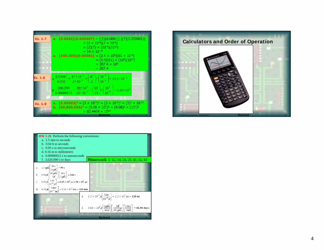
Calculators and Order of Operation
ET162 Circuit Analysis – Introduction Boylestad 13
HW 1-26 Perform the following conversions:a. 1.5 min to secondsb. 0.04 h to secondsc. 0.05 s to microsecondsd. 0.16 m to millimeterse. 0.00000012 s to nanosecondsf. 3,620,000 s to days Homework 1: 12, 14, 24, 26, 41, 42, 43
ET162 Circuit Analysis – Introduction Boylestad 14
1
Current and Voltage
Electrical and Telecommunications Engineering Technology Department
Professor Jang
EET1122/ET162 Circuit Analysis
Prepared by textbook based on “Introduction to Circuit Analysis”by Robert Boylestad, Prentice Hall, 10th edition.
OUTLINESOUTLINES
ET162 Circuit Analysis –Current and Voltage Boylestad 2
Resistance and Conductance
Ohmmeters
Current and Voltage
Ammeters and Voltmeters
Key Words: Resistance, Ohmmeter, Current, Voltage, Ammeter, Voltmeter
Introduction to Resistance
Figure 1.1 Resistance symbol and notation.
The flow of charge through any material encounters an opposing force similar in many aspect to mechanical friction. This opposition, due to the collisions between electrons and other atoms in the material, which converts electrical energy into another form of energy such as heat, is called the resistance of the material. The unit of measurement of resistance is the ohm (Ω).
ET162 Circuit Analysis –Current and Voltage Boylestad 3
FIGURE 1.2 Factors affecting the resistance of a conductor.
At a fixed temperature of 20°C (room temperature), the resistance is related to the other three factor by
ρ : resistivity of the sample (CM-ohms/ft at T=20°C)l : the length of the sample (feet)A : cross-sectional area of the sample (circular mils (CM))
(ohms, Ω)R lA
=ρ
ET162 Circuit Analysis –Current and Voltage Boylestad 4
2
Resistance: Circular Wires
FIGURE 1.3 Cases in which R2 > R1. For each case, all remaining parameters that control the resistance level are the same.
For two wires of the same physical size at the same temperature,
• the higher the resistivity (ρ), the more the resistance
• the longer the length of a conductor, the more the resistance
• the smaller the area of a conductor, the more the resistance
• the higher the temperature of a conductor, the more the resistance
ET162 Circuit Analysis –Current and Voltage Boylestad 5
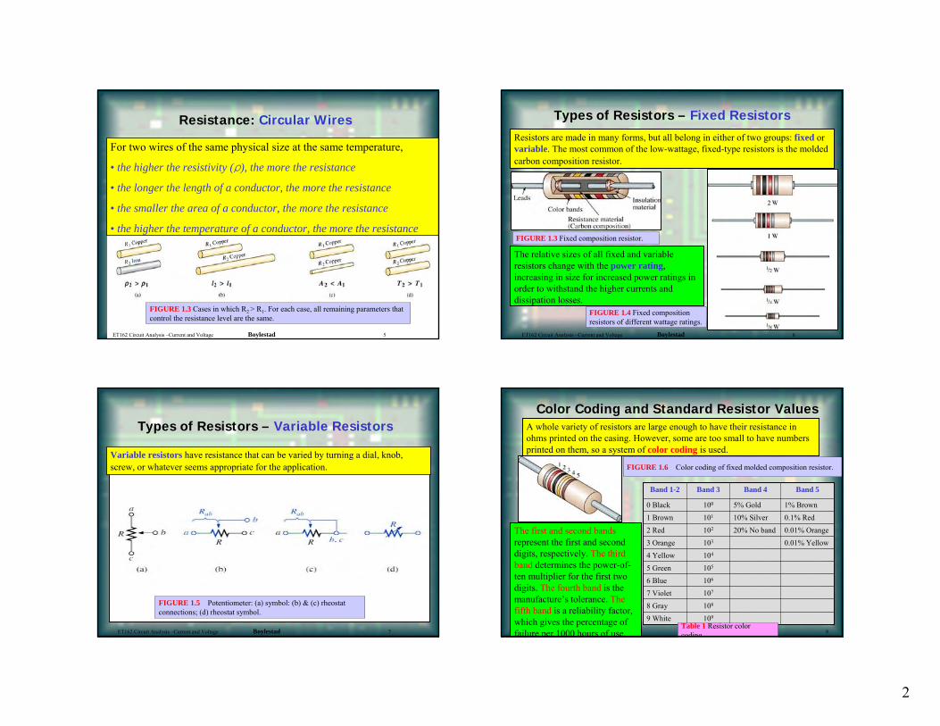
Types of Resistors – Fixed ResistorsResistors are made in many forms, but all belong in either of two groups: fixed or variable. The most common of the low-wattage, fixed-type resistors is the molded carbon composition resistor.
FIGURE 1.3 Fixed composition resistor.
FIGURE 1.4 Fixed composition resistors of different wattage ratings.
The relative sizes of all fixed and variable resistors change with the power rating, increasing in size for increased power ratings in order to withstand the higher currents and dissipation losses.
ET162 Circuit Analysis –Current and Voltage Boylestad 6
Types of Resistors – Variable Resistors
Variable resistors have resistance that can be varied by turning a dial, knob, screw, or whatever seems appropriate for the application.
FIGURE 1.5 Potentiometer: (a) symbol: (b) & (c) rheostat connections; (d) rheostat symbol.
ET162 Circuit Analysis –Current and Voltage Boylestad 7
Color Coding and Standard Resistor ValuesA whole variety of resistors are large enough to have their resistance in ohms printed on the casing. However, some are too small to have numbers printed on them, so a system of color coding is used.
ET162 Circuit Analysis – Voltage and Current Boylestad 8
FIGURE 1.6 Color coding of fixed molded composition resistor.
The first and second bandsrepresent the first and second digits, respectively. The third band determines the power-of-ten multiplier for the first two digits. The fourth band is the manufacture’s tolerance. The fifth band is a reliability factor, which gives the percentage of failure per 1000 hours of use.
1099 White1088 Gray1077 Violet1066 Blue1055 Green1044 Yellow
0.01% Yellow1033 Orange0.01% Orange20% No band1022 Red0.1% Red10% Silver1011 Brown1% Brown5% Gold1000 Black
Band 5Band 4Band 3Band 1-2
Table 1 Resistor color coding.
3
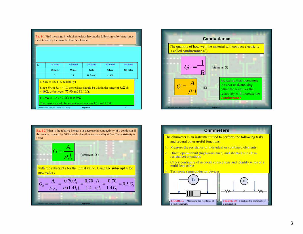
Ex. 1-1 Find the range in which a resistor having the following color bands must exist to satisfy the manufacturer’s tolerance:
a.
±10%10–1 = 0.193
No colorSilverGoldWhiteOrange
5th Band4th Band3rd Band2nd Band1st Bandb.
a. 82Ω± 5% (1% reliability)
Since 5% of 82 = 4.10, the resistor should be within the range of 82Ω±4.10Ω, or between 77.90 and 86.10Ω.
b. 3.9Ω ± 10% = 3.9Ω± 0.39Ω
The resistor should be somewhere between 3.51 and 4.29Ω.ET162 Circuit Analysis –Current and Voltage Boylestad 9
Conductance
The quantity of how well the material will conduct electricity is called conductance (S).
(siemens, S)GR
= 1
Indicating that increasing the area or decreasingeither the length or theresistivity will increase theConductance.
(S)G Al
=⋅ρ
ET162 Circuit Analysis –Current and Voltage Boylestad 10
Ex. 1-2 What is the relative increase or decrease in conductivity of a conductor if the area is reduced by 30% and the length is increased by 40%? The resistivity is fixed.
ii
i
lAGρ
=
with the subscript i for the initial value. Using the subscript n for new value :
iiii
i
ii
i
nn
nn G
GlA
lA
lAG 5.0
4.170.0
4.170.0
)4.1(70.0
=====ρρρ
ET162 Circuit Analysis –Current and Voltage Boylestad 11
(siemens, S)
OhmmetersThe ohmmeter is an instrument used to perform the following tasks
and several other useful functions.1. Measure the resistance of individual or combined elements2. Direct open-circuit (high-resistance) and short-circuit (low-
resistance) situations3. Check continuity of network connections and identify wires of a
multi-lead cable4. Test some semiconductor devices
FIGURE 1.8 Checking the continuity of a connection.
FIGURE 1.7 Measuring the resistance of a single element.
4
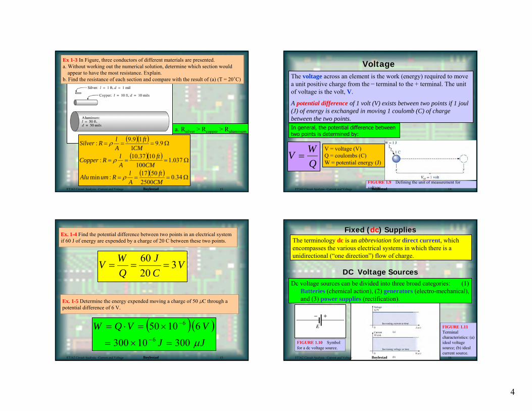
Ex 1-3 In Figure, three conductors of different materials are presented.a. Without working out the numerical solution, determine which section would
appear to have the most resistance. Explain.b. Find the resistance of each section and compare with the result of (a) (T = 20°C)
a. Rsilver > Rcopper > Raluminum
( )( )
( )( )
( )( )Ω===
Ω===
Ω===
34.02500
5017:min
037.1100
1037.10:
9.91
19.9:
CMft
AlRumAlu
CMft
AlRCopper
CMft
AlRSilver
ρ
ρ
ρ
ET162 Circuit Analysis –Current and Voltage Boylestad 13
VoltageThe voltage across an element is the work (energy) required to move a unit positive charge from the terminal to the + terminal. The unit of voltage is the volt, V.
A potential difference of 1 volt (V) exists between two points if 1 joul(J) of energy is exchanged in moving 1 coulomb (C) of charge between the two points.
FIGURE 1.9 Defining the unit of measurement for voltage.
In general, the potential difference between two points is determined by:
V = voltage (V)Q = coulombs (C)W = potential energy (J)
ET162 Circuit Analysis –Current and Voltage Boylestad 14
V WQ
=
Ex. 1-4 Find the potential difference between two points in an electrical system if 60 J of energy are expended by a charge of 20 C between these two points.
VCJ
QWV 3
2060
===
( )( )JJVVQW
µ3001030061050
6
6
=×=
×=⋅=−
−
Ex. 1-5 Determine the energy expended moving a charge of 50 μC through a potential difference of 6 V.
ET162 Circuit Analysis –Current and Voltage Boylestad 15
The terminology dc is an abbreviation for direct current, which encompasses the various electrical systems in which there is a unidirectional (“one direction”) flow of charge.
DC Voltage SourcesDc voltage sources can be divided into three broad categories: (1)
Batteries (chemical action), (2) generators (electro-mechanical), and (3) power supplies (rectification).
FIGURE 1.10 Symbol for a dc voltage source.
FIGURE 1.11Terminal characteristics: (a) ideal voltage source; (b) ideal current source.
Fixed (dc) Supplies
ET162 Circuit Analysis –Current and Voltage Boylestad 16
5
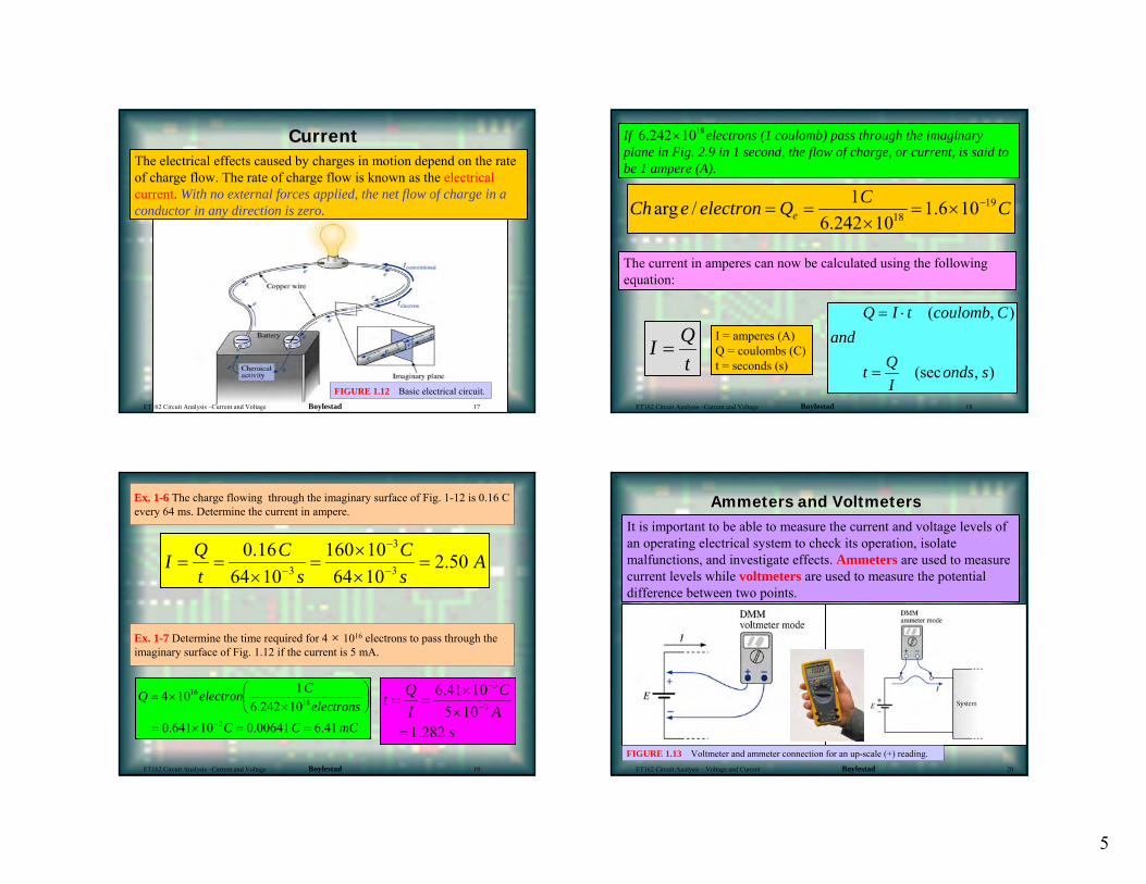
Current
FIGURE 1.12 Basic electrical circuit.
The electrical effects caused by charges in motion depend on the rate of charge flow. The rate of charge flow is known as the electrical current. With no external forces applied, the net flow of charge in a conductor in any direction is zero.
ET162 Circuit Analysis –Current and Voltage Boylestad 17
If electrons (1 coulomb) pass through the imaginary plane in Fig. 2.9 in 1 second, the flow of charge, or current, is said to be 1 ampere (A).
1810242.6 ×
CCQelectroneCh e19
18 106.110242.6
1/arg −×=×
==
tQI =
The current in amperes can now be calculated using the followingequation:
I = amperes (A)Q = coulombs (C)t = seconds (s) ),(sec
),(
sondsIQt
andCcoulombtIQ
=
⋅=
ET162 Circuit Analysis –Current and Voltage Boylestad 18
Ex. 1-6 The charge flowing through the imaginary surface of Fig. 1-12 is 0.16 C every 64 ms. Determine the current in ampere.
AsC
sC
tQI 50.2
106410160
106416.0
3
3
3 =××
=×
== −
−
−
mCCCelectrons
CelectronQ
41.600641.010641.010242.61104
2
1816
==×=
⎟⎠⎞
⎜⎝⎛
××=
−
Ex. 1-7 Determine the time required for 4 × 10¹⁶ electrons to pass through the imaginary surface of Fig. 1.12 if the current is 5 mA.
sAC
IQt
282.1105
1041.63
3
=××
== −
−
ET162 Circuit Analysis –Current and Voltage Boylestad 19
Ammeters and VoltmetersIt is important to be able to measure the current and voltage levels of an operating electrical system to check its operation, isolate malfunctions, and investigate effects. Ammeters are used to measure current levels while voltmeters are used to measure the potential difference between two points.
FIGURE 1.13 Voltmeter and ammeter connection for an up-scale (+) reading.ET162 Circuit Analysis – Voltage and Current Boylestad 20
1
Ohm’s Law
EET1122/ET162 Circuit Analysis
Electrical and Telecommunications Engineering Technology Department
Professor JangPrepared by textbook based on “Introduction to Circuit Analysis”
by Robert Boylestad, Prentice Hall, 10th edition.
AcknowledgementAcknowledgement
I want to express my gratitude to Prentice Hall giving me the permission to use instructor’s material for developing this module. I would like to thank the Department of Electrical and Telecommunications Engineering Technology of NYCCT for giving me support to commence and complete this module. I hope this module is helpful to enhance our students’ academic performance.
Sunghoon Jang
OUTLINESOUTLINES
Introduction to Ohm’s Law
Power
Plotting Ohm’s Law
ET162 Circuit Analysis – Ohm’s Law Boylestad 2
Key Words: Ohm’s Law, Current, Voltage, Power
Introduction to Ohm’s Law
Figure 4.1 Basic Circuit.
Ohm’s law clearly reveals that a fixed resistance, the greater the voltage across a resistor, the more the current, the more the resistance for the same voltage, the less the current.
V
RI
),(
),(
),(
Ω=
=
=
ohmsIER
VvoltsRIE
AamperesREI
ET162 Circuit Analysis – Ohm’s Law Boylestad 3
2
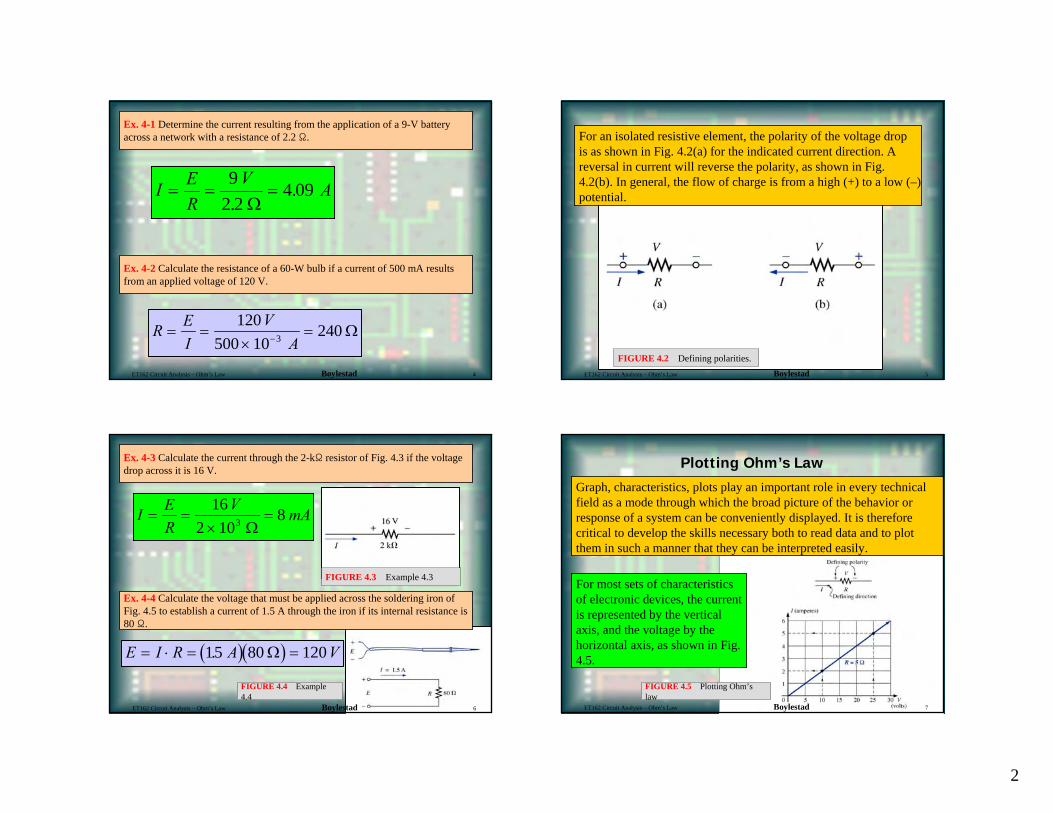
Ex. 4-1 Determine the current resulting from the application of a 9-V battery across a network with a resistance of 2.2 Ω.
I ER
VA= = =
92 2
4 09.
.Ω
Ex. 4-2 Calculate the resistance of a 60-W bulb if a current of 500 mA results from an applied voltage of 120 V.
R EI
VA
= =×
=−
120500 10
2403 Ω
ET162 Circuit Analysis – Ohm’s Law Boylestad 4
For an isolated resistive element, the polarity of the voltage drop is as shown in Fig. 4.2(a) for the indicated current direction. A reversal in current will reverse the polarity, as shown in Fig. 4.2(b). In general, the flow of charge is from a high (+) to a low (–) potential.
FIGURE 4.2 Defining polarities.ET162 Circuit Analysis – Ohm’s Law Boylestad 5
I ER
VmA= =
×=
162 10
83 Ω
Ex. 4-3 Calculate the current through the 2-kΩ resistor of Fig. 4.3 if the voltage drop across it is 16 V.
Ex. 4-4 Calculate the voltage that must be applied across the soldering iron of Fig. 4.5 to establish a current of 1.5 A through the iron if its internal resistance is 80 Ω.
( )( )E I R A V= ⋅ = =15 80 120. Ω
FIGURE 4.3 Example 4.3
FIGURE 4.4 Example 4.4
ET162 Circuit Analysis – Ohm’s Law Boylestad 6
Plotting Ohm’s LawGraph, characteristics, plots play an important role in every technical field as a mode through which the broad picture of the behavior or response of a system can be conveniently displayed. It is therefore critical to develop the skills necessary both to read data and to plot them in such a manner that they can be interpreted easily.
For most sets of characteristics of electronic devices, the current is represented by the vertical axis, and the voltage by the horizontal axis, as shown in Fig. 4.5.
FIGURE 4.5 Plotting Ohm’s law
ET162 Circuit Analysis – Ohm’s Law Boylestad 7
3
R VIdc =
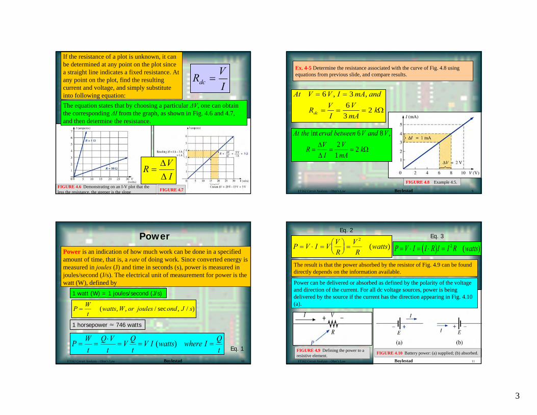
If the resistance of a plot is unknown, it can be determined at any point on the plot since a straight line indicates a fixed resistance. At any point on the plot, find the resulting current and voltage, and simply substitute into following equation:The equation states that by choosing a particular ∆V, one can obtain the corresponding ∆I from the graph, as shown in Fig. 4.6 and 4.7, and then determine the resistance.
FIGURE 4.6 Demonstrating on an I-V plot that the less the resistance, the steeper is the slope FIGURE 4.7
RVI
=∆∆
FIGURE 4.8 Example 4.5.
Ex. 4-5 Determine the resistance associated with the curve of Fig. 4.8 using equations from previous slide, and compare results.
At V V I mA and
R VI
VmA
kdc
= =
= = =
6 36
32
, ,
Ω
At the erval between V and V
R VI
VmA
k
int ,6 82
12= = =
∆∆
Ω
ET162 Circuit Analysis – Ohm’s Law Boylestad 9
Power
P Wt
watts W or joules ond J s= ( , , / sec , / )
Power is an indication of how much work can be done in a specified amount of time, that is, a rate of doing work. Since converted energy is measured in joules (J) and time in seconds (s), power is measured in joules/second (J/s). The electrical unit of measurement for power is the watt (W), defined by
1 watt (W) = 1 joules/second (J/s)
1 horsepower ≈ 746 watts
P Wt
Q Vt
V Qt
V I watts where I Qt
= =⋅
= = =( )Eq. 1
ET162 Circuit Analysis – Ohm’s Law Boylestad 10
FIGURE 4.9 Defining the power to a resistive element.
P V I V VR
VR
watts= ⋅ = ⎛⎝⎜
⎞⎠⎟=
2
( ) ( )P V I I R I I R watts= ⋅ = ⋅ = 2 ( )
Eq. 2Eq. 3
The result is that the power absorbed by the resistor of Fig. 4.9 can be found directly depends on the information available.
Power can be delivered or absorbed as defined by the polarity of the voltage and direction of the current. For all dc voltage sources, power is being delivered by the source if the current has the direction appearing in Fig. 4.10 (a).
FIGURE 4.10 Battery power: (a) supplied; (b) absorbed.
ET162 Circuit Analysis – Ohm’s Law Boylestad 11
4
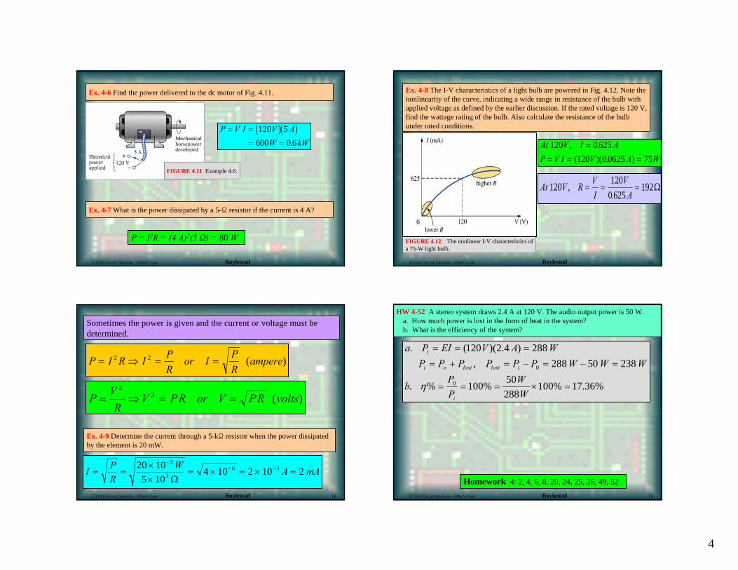
Ex. 4-6 Find the power delivered to the dc motor of Fig. 4.11.
( )( )P V I V AW kW
= =
= =
120 5600 0 6.
FIGURE 4.11 Example 4.6.
Ex. 4-7 What is the power dissipated by a 5-Ω resistor if the current is 4 A?
P = I2R = (4 A)2(5 Ω) = 80 W
ET162 Circuit Analysis – Ohm’s Law Boylestad 12
FIGURE 4.12 The nonlinear I-V characteristics of a 75-W light bulb.
Ex. 4-8 The I-V characteristics of a light bulb are powered in Fig. 4.12. Note thenonlinearity of the curve, indicating a wide range in resistance of the bulb with applied voltage as defined by the earlier discussion. If the rated voltage is 120 V, find the wattage rating of the bulb. Also calculate the resistance of the bulb under rated conditions.
At V I AP V I V A W
120 0 625120 0 0625 75
, .( )( . )
== = =
At V R VI
VA
120 1200 625
192,.
= = = Ω
ET162 Circuit Analysis – Ohm’s Law Boylestad 13
Sometimes the power is given and the current or voltage must be determined.
P I R I PR
or I PR
ampere= ⇒ = =2 2 ( )
P VR
V PR or V PR volts= ⇒ = =2
2 ( )
Ex. 4-9 Determine the current through a 5-kΩ resistor when the power dissipated by the element is 20 mW.
I PR
WA mA= =
××
= × = × =−
− −20 105 10
4 10 2 10 23
36 3
ΩET162 Circuit Analysis – Ohm’s Law Boylestad 14
HW 4-52 A stereo system draws 2.4 A at 120 V. The audio output power is 50 W.a. How much power is lost in the form of heat in the system?b. What is the efficiency of the system?
Homework 4: 2, 4, 6, 8, 20, 24, 25, 26, 49, 52
%36.17%10028850%100%.
23850288,288)4.2)(120(.
0
0
=×===
=−=−=+====
WW
PP
b
WWWPPPPPPWAVEIPa
i
ilostlostoi
i
η
ET162 Circuit Analysis – Ohm’s Law Boylestad 15
1
Series Circuits
EET1122/ET162 Circuit Analysis
Electrical and Telecommunications Engineering Technology Department
Professor JangPrepared by textbook based on “Introduction to Circuit Analysis”
by Robert Boylestad, Prentice Hall, 10th edition.
AcknowledgementAcknowledgement
I want to express my gratitude to Prentice Hall giving me the permission to use instructor’s material for developing this module. I would like to thank the Department of Electrical and Telecommunications Engineering Technology of NYCCT for giving me support to commence and complete this module. I hope this module is helpful to enhance our students’ academic performance.
Sunghoon Jang
OUTLINESOUTLINESIntroduction to Series Circuits
ET162 Circuit Analysis – Series Circuits Boylestad 2
Kirchhoff’s Voltage Law
Interchanging Series Elements
Ideal dc Voltage Sources vs. Non-ideal Sources
Voltage Divider Rule
Series Circuits – Notation
Voltage Regulation
Key Words: Series Circuit, Kirchhoff’s Voltage Law, Voltage Divider Rule
Series Circuits - Introduction
Two types of current are available to the consumer today. One is direct current (dc), in which ideally the flow of charge (current) does not change in magnitude with time. The other is sinusoidal alternating current (ac), in which the flow of charge is continually changing in magnitude with time.
FIGURE 5.1 Introducing the basic components of an electric circuit.
V (volt) = E (volt)
ET162 Circuit Analysis – Series Circuits Boylestad 3
2
ET162 Circuit Analysis – Ohm’s Law and Series Current Floyd 4
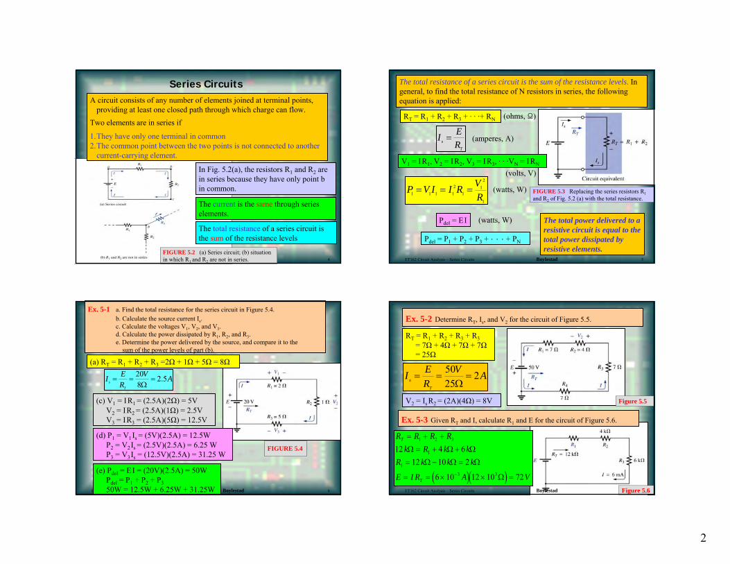
Series CircuitsA circuit consists of any number of elements joined at terminal points,
providing at least one closed path through which charge can flow.Two elements are in series if
1.They have only one terminal in common2.The common point between the two points is not connected to another
current-carrying element.
FIGURE 5.2 (a) Series circuit; (b) situation in which R1 and R2 are not in series.
The current is the same through series elements.
The total resistance of a series circuit is the sum of the resistance levels
In Fig. 5.2(a), the resistors R1 and R2 are in series because they have only point b in common.
T
s REI =
1
21
12
1111 RVRIIVP ===
The total resistance of a series circuit is the sum of the resistance levels. In general, to find the total resistance of N resistors in series, the following equation is applied:
RT = R1 + R2 + R3 + · · ·+ RN
(amperes, A)
Pdel = EI
Pdel = P1 + P2 + P3 + · · · + PN
The total power delivered to a resistive circuit is equal to the total power dissipated by resistive elements.
V1 = IR1, V2 = IR2, V3 = IR3, · · ·VN = IRN
(volts, V)
(ohms, Ω)
FIGURE 5.3 Replacing the series resistors R1and R2 of Fig. 5.2 (a) with the total resistance.
(watts, W)
(watts, W)
ET162 Circuit Analysis – Series Circuits Boylestad 5
ET162 Circuit Analysis – Ohm’s Law and Series Current Boylestad 6
AVREI
T
s 5.2820
=Ω
==
Ex. 5-1 a. Find the total resistance for the series circuit in Figure 5.4.b. Calculate the source current Is.c. Calculate the voltages V1, V2, and V3.d. Calculate the power dissipated by R1, R2, and R3.e. Determine the power delivered by the source, and compare it to the
sum of the power levels of part (b).
(a) RT = R1 + R2 + R3 =2Ω + 1Ω + 5Ω = 8Ω
(c) V1 = IR1 = (2.5A)(2Ω) = 5VV2 = IR2 = (2.5A)(1Ω) = 2.5VV3 = IR3 = (2.5A)(5Ω) = 12.5V
(d) P1 = V1Is = (5V)(2.5A) = 12.5WP2 = V2Is = (2.5V)(2.5A) = 6.25 WP3 = V3Is = (12.5V)(2.5A) = 31.25 W
(e) Pdel = EI = (20V)(2.5A) = 50WPdel = P1 + P2 + P350W = 12.5W + 6.25W + 31.25W
FIGURE 5.4
Ex. 5-2 Determine RT, Is, and V2 for the circuit of Figure 5.5.
AVREI
T
s 22550
=Ω
==
RT = R1 + R2 + R3 + R3= 7Ω + 4Ω + 7Ω + 7Ω= 25Ω
V2 = Is R2 = (2A)(4Ω) = 8V Figure 5.5
Ex. 5-3 Given RT and I, calculate R1 and E for the circuit of Figure 5.6.
( )( )
R R R Rk R k k
R k k k
E I R A V
T
T
= + += + +
= − =
= = × × =−
1 2 3
1
1
3 3
12 4 612 10 2
6 10 12 10 72
Ω Ω ΩΩ Ω Ω
ΩFigure 5.6ET162 Circuit Analysis – Series Circuits Boylestad
3
ET = E1 + E2 + E3 = 10V + 6V + 2V = 18V
ET = E2 + E3 – E1 = 9V +3V – 4V = 8V
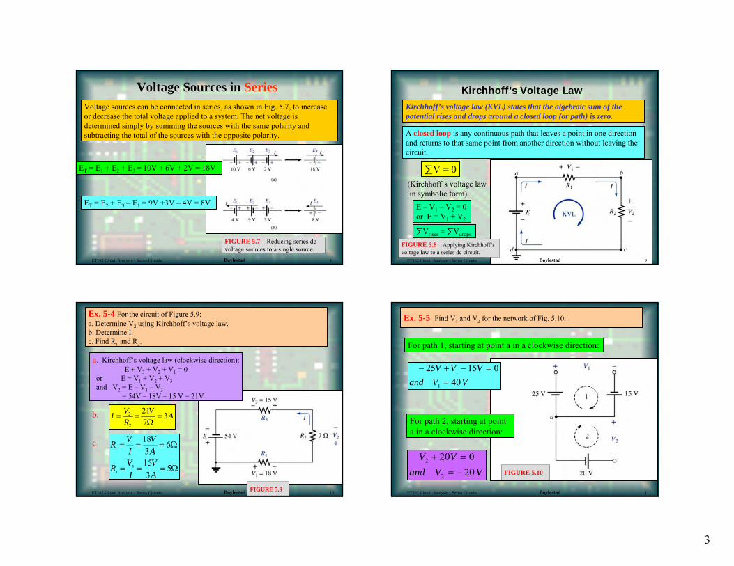
FIGURE 5.7 Reducing series dc voltage sources to a single source.
Voltage Sources in SeriesVoltage sources can be connected in series, as shown in Fig. 5.7, to increase or decrease the total voltage applied to a system. The net voltage is determined simply by summing the sources with the same polarity and subtracting the total of the sources with the opposite polarity.
ET162 Circuit Analysis – Series Circuits Boylestad 8
Kirchhoff’s Voltage LawKirchhoff’s voltage law (KVL) states that the algebraic sum of the potential rises and drops around a closed loop (or path) is zero.
A closed loop is any continuous path that leaves a point in one direction and returns to that same point from another direction without leaving the circuit.
∑V = 0(Kirchhoff’s voltage lawin symbolic form)
FIGURE 5.8 Applying Kirchhoff’s voltage law to a series dc circuit.
E – V1 – V2 = 0or E = V1 + V2
∑Vrises = ∑Vdrops
ET162 Circuit Analysis – Series Circuits Boylestad 9
Ex. 5-4 For the circuit of Figure 5.9:a. Determine V2 using Kirchhoff’s voltage law.b. Determine I.c. Find R1 and R2.
b. AVRVI 3
721
2
2 =Ω
==
Ω===
Ω===
53
15
63
18
33
11
AV
IVR
AV
IVRc.
a. Kirchhoff’s voltage law (clockwise direction):– E + V3 + V2 + V1 = 0
or E = V1 + V2 + V3and V2 = E – V1 – V3
= 54V – 18V – 15 V = 21V
FIGURE 5.9ET162 Circuit Analysis – Series Circuits Boylestad 10
Ex. 5-5 Find V1 and V2 for the network of Fig. 5.10.
− + − ==
25 15 040
1
1
V V Vand V V
For path 1, starting at point a in a clockwise direction:
For path 2, starting at point a in a clockwise direction:
V Vand V V
2
2
20 020
+ == − FIGURE 5.10
ET162 Circuit Analysis – Series Circuits Boylestad 11
4
− + + − ==
60 40 30 050
V V V Vand V V
x
x
Ex. 5-6 Using Kirchhoff’s voltage law, determine the unknown voltage for the network of Fig. 5.11.
6 14 2 018
V V V Vand V V
x
x
+ + − == −
FIGURE 5.11
ET162 Circuit Analysis – Series Circuits Boylestad 12
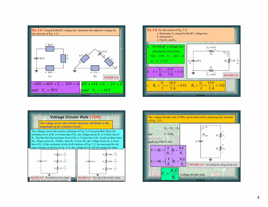
Ex. 5-8 For the circuit of Fig. 5.12.a. Determine V2 using Kirchhoff’s voltage law.b. Determine I.c. Find R1 and R3.
a Kirchhoff s voltage lawclockwise directionV V V V
or V V
. '( ):
54 15 18 021
2
2
− − − ==
b I VR
V A. = = =2
2
217
3Ω
c R VI
VA
R VI
VA
. 11
3318
36 15
35= = = = = =Ω Ω
FIGURE 5.12
ET162 Circuit Analysis – Series Circuits Boylestad 13
Voltage Divider Rule (VDR)The voltage across the resistive elements will divide as the magnitude of the resistance levels.
FIGURE 5.13 Revealing how the voltage will divide across series resistive elements.
FIGURE 5.14 The ratio of the resistive values determines the voltage division of a series dc circuit.
The voltages across the resistive elements of Fig. 5.13 are provided. Since the resistance level of R1 is 6 times that of R3, the voltage across R1 is 6 times that of R3. The fact that the resistance level of R2 is 3 times that of R1 results in three times the voltage across R2. Finally, since R1 is twice R2, the voltage across R1 is twice that of R2. If the resistance levels of all resistors of Fig. 5.13 are increased by the same amount, as shown in Fig. 5.14, the voltage levels will all remain the same.
The voltage divider rule (VDR) can be derived by analyzing the network of Fig. 5.15.
TT
TT
RERR
REIRV
RERR
REIRV
2222
1111
=⎟⎟⎠
⎞⎜⎜⎝
⎛==
=⎟⎟⎠
⎞⎜⎜⎝
⎛==
T
xx R
ERV =
RT = R1 + R2
and I = E/RT
Applying Ohm’s law:
(voltage divider rule)
FIGURE 5.15 Developing the voltage divider rule.
ET162 Circuit Analysis – Series Circuits Boylestad 15
5
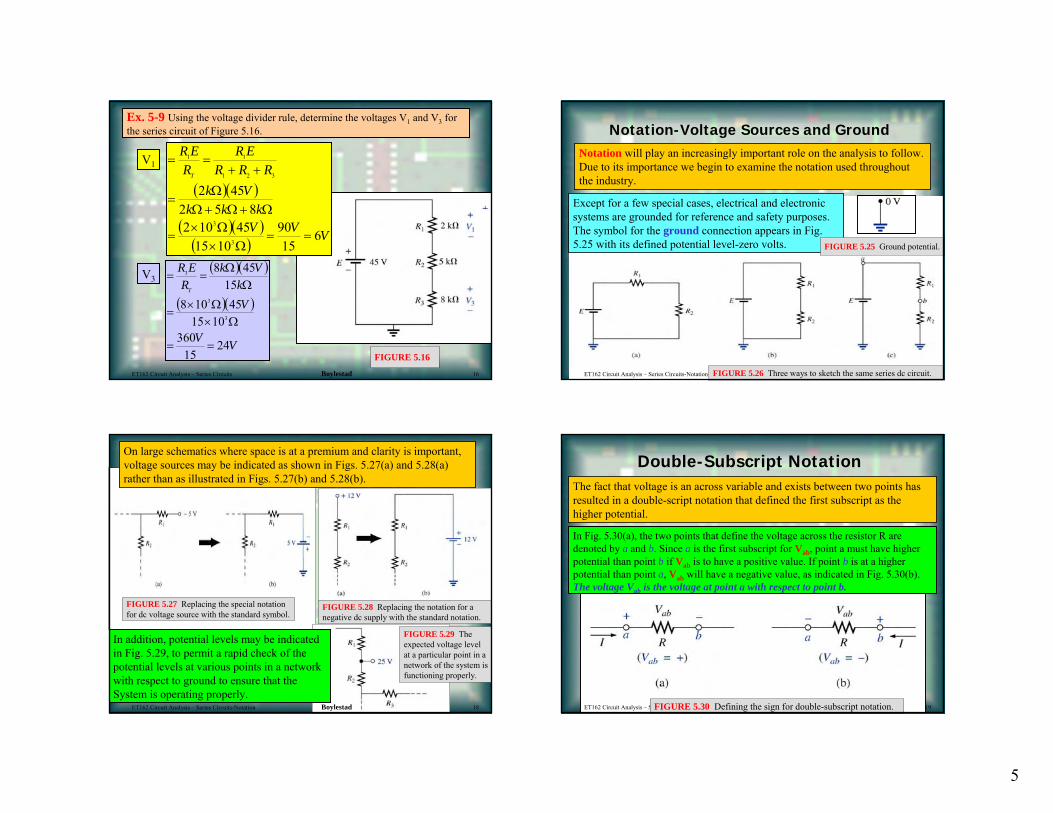
Ex. 5-9 Using the voltage divider rule, determine the voltages V1 and V3 for the series circuit of Figure 5.16.
( )( )
( )( )( ) VVV
kkkVk
RRRER
RERT
615
901015
45102852
452
3
3
321
11
==Ω×
Ω×=
Ω+Ω+ΩΩ
=
++==
( )( )
( )( )
VV
Vk
VkR
ERT
2415
3601015
4510815
458
3
3
3
==
Ω×Ω×=
ΩΩ
==
V1
V3
FIGURE 5.16
ET162 Circuit Analysis – Series Circuits Boylestad 16
Notation-Voltage Sources and GroundNotation will play an increasingly important role on the analysis to follow. Due to its importance we begin to examine the notation used throughout the industry.
Except for a few special cases, electrical and electronic systems are grounded for reference and safety purposes. The symbol for the ground connection appears in Fig. 5.25 with its defined potential level-zero volts. FIGURE 5.25 Ground potential.
ET162 Circuit Analysis – Series Circuits-Notation Boylestad 2FIGURE 5.26 Three ways to sketch the same series dc circuit.
FIGURE 5.27 Replacing the special notation for dc voltage source with the standard symbol.
On large schematics where space is at a premium and clarity is important, voltage sources may be indicated as shown in Figs. 5.27(a) and 5.28(a) rather than as illustrated in Figs. 5.27(b) and 5.28(b).
FIGURE 5.28 Replacing the notation for a negative dc supply with the standard notation.
In addition, potential levels may be indicatedin Fig. 5.29, to permit a rapid check of the potential levels at various points in a networkwith respect to ground to ensure that the System is operating properly.
FIGURE 5.29 The expected voltage level at a particular point in a network of the system is functioning properly.
ET162 Circuit Analysis – Series Circuits-Notation Boylestad 18
Double-Subscript NotationThe fact that voltage is an across variable and exists between two points has resulted in a double-script notation that defined the first subscript as the higher potential.
In Fig. 5.30(a), the two points that define the voltage across the resistor R are denoted by a and b. Since a is the first subscript for Vab, point a must have higher potential than point b if Vab is to have a positive value. If point b is at a higher potential than point a, Vab will have a negative value, as indicated in Fig. 5.30(b). The voltage Vab is the voltage at point a with respect to point b.
ET162 Circuit Analysis – Series Circuits-Notation Floyd 19FIGURE 5.30 Defining the sign for double-subscript notation.
6
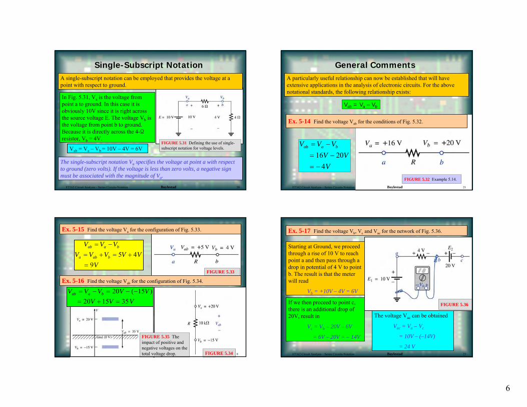
Single-Subscript Notation
In Fig. 5.31, Va is the voltage from point a to ground. In this case it is obviously 10V since it is right across the source voltage E. The voltage Vb is the voltage from point b to ground. Because it is directly across the 4-Ωresistor, Vb = 4V.
A single-subscript notation can be employed that provides the voltage at a point with respect to ground.
FIGURE 5.31 Defining the use of single-subscript notation for voltage levels.
The single-subscript notation Va specifies the voltage at point a with respect to ground (zero volts). If the voltage is less than zero volts, a negative sign must be associated with the magnitude of Va.
Vab = Va – Vb = 10V – 4V = 6V
ET162 Circuit Analysis – Series Circuits-Notation Boylestad 20
FIGURE 5.32 Example 5.14.
General CommentsA particularly useful relationship can now be established that will have extensive applications in the analysis of electronic circuits. For the above notational standards, the following relationship exists:
Vab = Va – Vb
Ex. 5-14 Find the voltage Vab for the conditions of Fig. 5.32.
V V VV VV
ab a b= −= −= −
16 204
ET162 Circuit Analysis – Series Circuits-Notation Boylestad 21
FIGURE 5.34
Ex. 5-15 Find the voltage Va for the configuration of Fig. 5.33.
V V VV V V V V
V
ab a b
a ab b
= −= + = +=
5 49
V V V V VV V V
ab a b= − = − −= + =
20 1520 15 35
( )Ex. 5-16 Find the voltage Vab for the configuration of Fig. 5.34.
FIGURE 5.33
Floyd 8
FIGURE 5.35 The impact of positive and negative voltages on the total voltage drop.
Ex. 5-17 Find the voltage Vb, Vc and Vac for the network of Fig. 5.36.
Starting at Ground, we proceed through a rise of 10 V to reach point a and then pass through a drop in potential of 4 V to point b. The result is that the meter will read
Vb = +10V – 4V = 6V
FIGURE 5.36If we then proceed to point c, there is an additional drop of 20V, result in
Vc = Vb – 20V – 6V
= 6V – 20V = – 14V
The voltage Vac can be obtained
Vac = Va – Vc
= 10V – (–14V)
= 24 VET162 Circuit Analysis – Series Circuits-Notation Boylestad 23
7
I E ER
V V V A
and V V V V V VT
ab cb c
=+
=+
= =
= = − = −
1 2 19 3545
5445
12
30 24 19Ω Ω
.
ET162 Circuit Analysis – Series Circuits Floyd 24
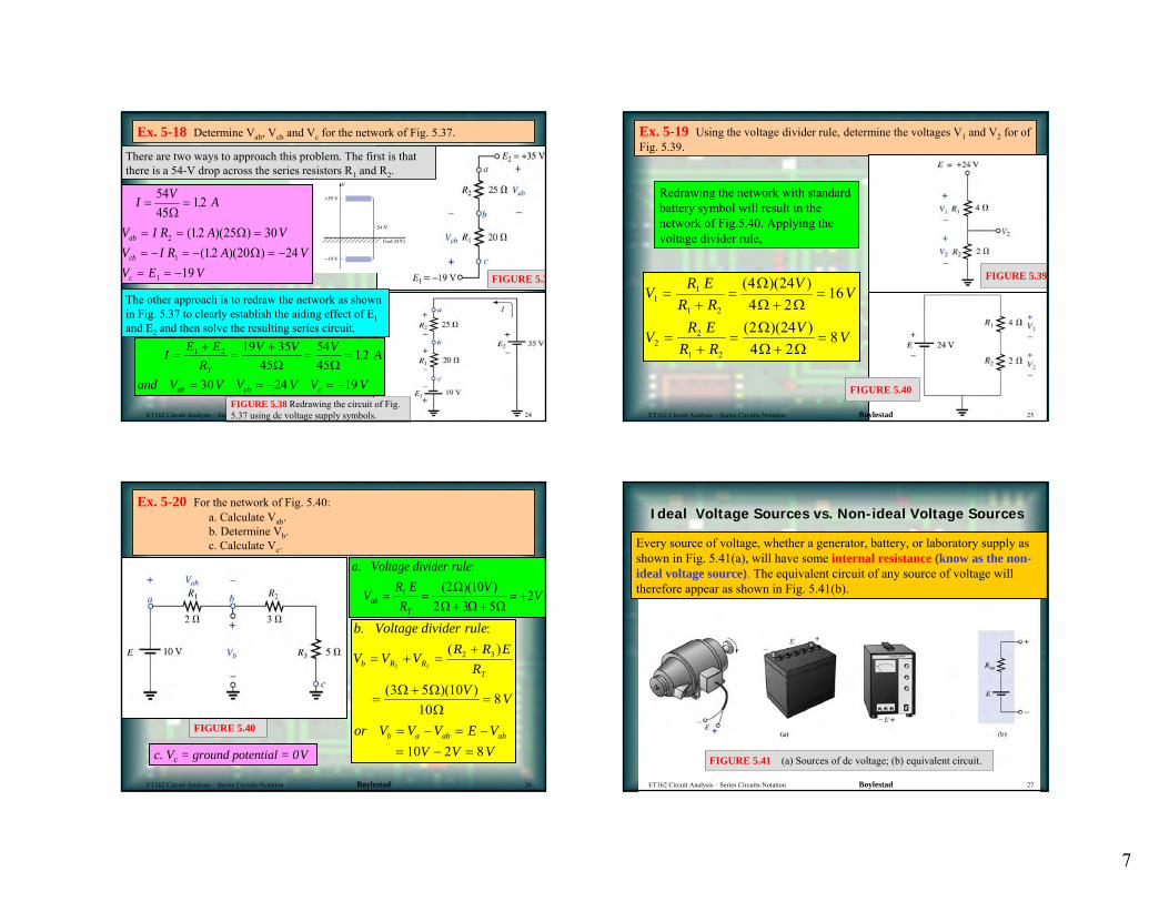
Ex. 5-18 Determine Vab, Vcb and Vc for the network of Fig. 5.37.
FIGURE 5.38 Redrawing the circuit of Fig. 5.37 using dc voltage supply symbols.
IV
A
V I R A VV I R A VV E V
ab
cb
c
= =
= = == − = − = −= = −
5445
12
12 25 3012 20 24
19
2
1
1
ΩΩ
Ω
.
( . )( )( . )( )
The other approach is to redraw the network as shown in Fig. 5.37 to clearly establish the aiding effect of E1and E2 and then solve the resulting series circuit.
There are two ways to approach this problem. The first is that there is a 54-V drop across the series resistors R1 and R2.
FIGURE 5.3
Redrawing the network with standard battery symbol will result in the network of Fig.5.40. Applying the voltage divider rule,
FIGURE 5.40
Ex. 5-19 Using the voltage divider rule, determine the voltages V1 and V2 for of Fig. 5.39.
VR E
R RV
V
VR E
R RV
V
11
1 2
22
1 2
4 244 2
16
2 244 2
8
=+
=+
=
=+
=+
=
( )( )
( )( )
ΩΩ ΩΩΩ Ω
FIGURE 5.39
ET162 Circuit Analysis – Series Circuits-Notation Boylestad 25
FIGURE 5.40
Ex. 5-20 For the network of Fig. 5.40:a. Calculate Vab.b. Determine Vb.c. Calculate Vc.
a Voltage divider rule
VR ER
VVab
T
. :( )( )
= =+ +
= +1 2 102 3 5
2Ω
Ω Ω Ω
b Voltage divider rule
V V VR R E
RV
V
or V V V E VV V V
b R RT
b a ab ab
. :( )
( )( )
= + =+
=+
=
= − = −= − =
2 3
2 3
3 5 1010
8
10 2 8
Ω ΩΩ
c. Vc = ground potential = 0V
ET162 Circuit Analysis – Series Circuits-Notation Boylestad 26
Every source of voltage, whether a generator, battery, or laboratory supply as shown in Fig. 5.41(a), will have some internal resistance (know as the non-ideal voltage source). The equivalent circuit of any source of voltage will therefore appear as shown in Fig. 5.41(b).
FIGURE 5.41 (a) Sources of dc voltage; (b) equivalent circuit.
Ideal Voltage Sources vs. Non-ideal Voltage Sources
ET162 Circuit Analysis – Series Circuits-Notation Boylestad 27
8
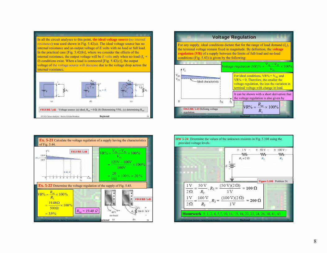
In all the circuit analyses to this point, the ideal voltage source (no internal resistance) was used shown in Fig. 5.42(a). The ideal voltage source has no internal resistance and an output voltage of E volts with no load or full load. In the practical case [Fig. 5.42(b)], where we consider the effects of the internal resistance, the output voltage will be E volts only when no-load (IL = 0) conditions exist. When a load is connected [Fig. 5.42(c)], the output voltage of the voltage source will decrease due to the voltage drop across the internal resistance.
FIGURE 5.42 Voltage source: (a) ideal, Rint = 0 Ω; (b) Determining VNL; (c) determining Rint.
ET162 Circuit Analysis – Series Circuits-Notation Boylestad 28
Voltage regulation VR V VV
NL FL
FL
( )% =−
×100%
VR RRL
% int= ×100%FIGURE 5.43 Defining voltage regulation.
Voltage Regulation
For any supply, ideal conditions dictate that for the range of load demand (IL), the terminal voltage remain fixed in magnitude. By definition, the voltage regulation (VR) of a supply between the limits of full-load and no-load conditions (Fig. 5.43) is given by the following:
For ideal conditions, VR% = VNL and VR% = 0. Therefore, the smaller the voltage regulation, the less the variation in terminal voltage with change in load.
It can be shown with a short derivation that the voltage regulation is also given by
ET162 Circuit Analysis – Series Circuits-Notation Boylestad 29
Ex. 5-21 Calculate the voltage regulation of a supply having the characteristics of Fig. 5.44.
VR V VVV V
V
NL FL
FL
% %
%
% %
=−
×
=−
×
= × =
100
120 100100
100
20100
100 20
VR RRL
% %
.%
. %
int= ×
= ×
=
100
19 48500
100
39
ΩΩ
FIGURE 5.44
FIGURE 5.45
Ex. 5-22 Determine the voltage regulation of the supply of Fig. 5.45.
Rint = 19.48 Ω
ET162 Circuit Analysis – Series Circuits-Notation Boylestad 30
HW 5-24 Determine the values of the unknown resistors in Fig. 5.108 using the provided voltage levels.
Homework 5: 1, 2, 4, 5,7, 10, 11, 15, 16, 22, 23, 24, 26, 30, 41, 43
Figure 5.108 Problem 24.
ET162 Circuit Analysis – Series Circuits-Notation Boylestad 31
1
Parallel Circuits
EET1122/ET162 Circuit Analysis
Electrical and Telecommunications Engineering Technology Department
Professor JangPrepared by textbook based on “Introduction to Circuit Analysis”
by Robert Boylestad, Prentice Hall, 10th edition.
OUTLINESOUTLINES
Introduction to Parallel circuits analysis
Parallel Elements
Total Conductance and Resistance
Parallel circuits analysis and measurements
ET162 Circuit Analysis – Parallel Circuits Boylestad 2
Kirchhoff’s Current Law
Current Divider Rule
Voltage Sources in Parallel
Key Words: Parallel Circuit, Kirchhoff’s Current Law, Current Divider Rule, Voltage Source
ET162 Circuit Analysis – Parallel Circuits Boylestad 3
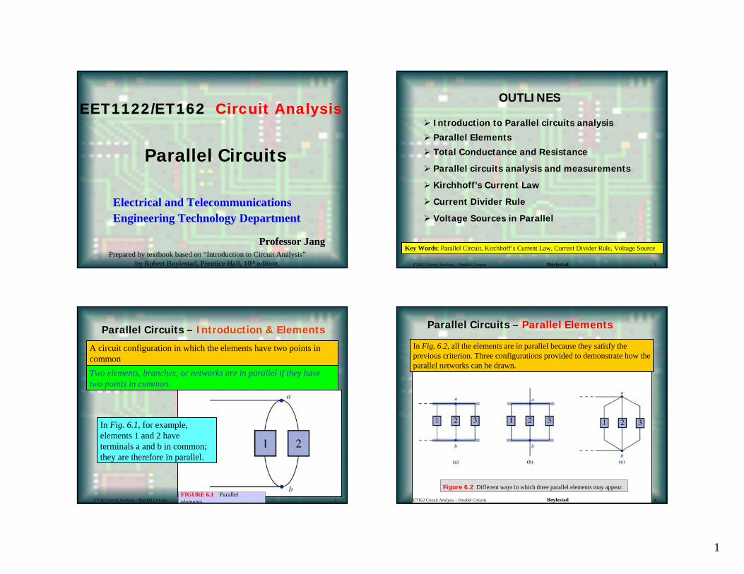
Parallel Circuits – Introduction & Elements
A circuit configuration in which the elements have two points incommonTwo elements, branches, or networks are in parallel if they havetwo points in common.
FIGURE 6.1 Parallel elements.
In Fig. 6.1, for example, elements 1 and 2 have terminals a and b in common; they are therefore in parallel.
Parallel Circuits – Parallel Elements
In Fig. 6.2, all the elements are in parallel because they satisfy the previous criterion. Three configurations provided to demonstrate how the parallel networks can be drawn.
Figure 6.2 Different ways in which three parallel elements may appear.
ET162 Circuit Analysis – Parallel Circuits Boylestad 4
2
Parallel Circuits – Parallel Elements
In Fig. 6.3, elements 1 and 2 are in parallel because they have terminals aand b in common. The parallel combination of 1 and 2 is then in series with element 3 due to the common terminal point b.
In Fig. 6.4, elements 1 and 2 are in series due to the common point a, but the series combination of 1 and 2 is in parallel with elements 3 as defined by the common terminal connections at a and b.
Figure 6.3 Network in which 1 and 2 are in parallel and 3 is in series with the parallel combination of 1 and 2.
Figure 6.4 Network in which 1 and 2 are in series and 3 is in parallel.
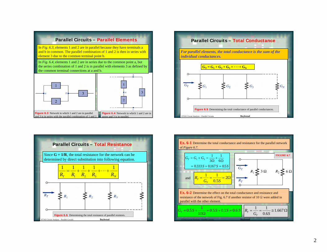
Parallel Circuits – Total Conductance
For parallel elements, the total conductance is the sum of the individual conductances.
GT = G1 + G2 + G3 + · · · + GN
Figure 6.5 Determining the total conductance of parallel conductances.
ET162 Circuit Analysis – Parallel Circuits Boylestad 6
Parallel Circuits – Total Resistance
Since G = 1/R, the total resistance for the network can be determined by direct substitution into following equation.
Figure 6.6 Determining the total resistance of parallel resistors.
NT RRRRR11111
321
+⋅⋅⋅+++=
ET162 Circuit Analysis – Parallel Circuits Boylestad 7
Ω=== 25.011
SGR
TT
Ex. 6-1 Determine the total conductance and resistance for the parallel network of Figure 6.7.
and
Ex. 6-2 Determine the effect on the total conductance and resistance andresistance of the network of Fig. 6.7 if another resistor of 10 Ω were added in parallel with the other element.
SSSSGT 6.01.05.010
15.0 =+=Ω
+= Ω≅== 667.16.011
SGR
TT
FIGURE 6.7G G G
S S S
T = + = +
= + =
1 21
31
60 333 0167 05
Ω Ω. . .
ET162 Circuit Analysis – Parallel Circuits Boylestad 8
3
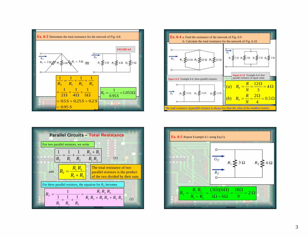
Ex. 6-3 Determine the total resistance for the network of Fig. 6.8.
FIGURE 6.8
Ω== 053.195.01
SRT
1 1 1 1
12
14
15
05 0 25 0 20 95
1 2 2R R R R
S S SS
T
= + +
= + +
= + +=
Ω Ω Ω. . ..
ET162 Circuit Analysis – Parallel Circuits Boylestad 9
Ex. 6-4 a. Find the resistance of the network of Fig. 6.9.b. Calculate the total resistance for the network of Fig. 6.10.
Figure 6.9 Example 6-4: three parallel resistorsFigure 6.10 Example 6-4: four parallel resistors of equal value.
Ω=Ω
==
Ω=Ω
==
5.04
2)(
43
12)(
NRRb
NRRa
T
T
The total resistance of parallel resistors is always less than the value of the smallest resistor.
Parallel Circuits – Total Resistance
21
12
21
111RRRR
RRRT
+=+=
For two parallel resistors, we write
21
21
RRRRRT +
=and
For three parallel resistors, the equation for RT becomes
The total resistance of two parallel resistors is the product of the two divided by their sum.
R
R R R
R R RR R R R R RT =
+ +=
+ +1
1 1 1
1 2 3
1 2 3
1 2 1 3 2 3
(1)
(2)
ET162 Circuit Analysis – Parallel Circuits Boylestad 11
Ex. 6-5 Repeat Example 6.1 using Eq.(1).
R R RR RT =
+=
+= =1 2
1 2
3 63 6
189
2( )( )Ω ΩΩ Ω
ΩΩ
ET162 Circuit Analysis – Parallel Circuits Boylestad 12
4
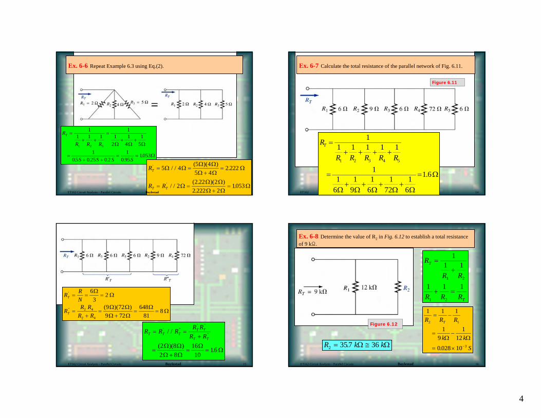
Ex. 6-6 Repeat Example 6.3 using Eq.(2).
R
R R R
S S S S
T =+ +
=+ +
=+ +
= =
11 1 1
11
21
41
51
05 0 25 0 21
0 951053
1 2 3 Ω Ω Ω
Ω. . . .
.
R
R R
T
T T
'
'
/ /(5 )( )
.
/ /( . )( ).
.
= =+
=
= =+
=
5 44
5 42 222
22 22 2
2 222 21053
Ω ΩΩ ΩΩ Ω
Ω
ΩΩ ΩΩ Ω
ΩET162 Circuit Analysis – Parallel Circuits Boylestad
Ex. 6-7 Calculate the total resistance of the parallel network of Fig. 6.11.
Figure 6.11
Ω=
Ω+
Ω+
Ω+
Ω+
Ω
=
++++=
6.1
61
721
61
91
61
1
111111
54321 RRRRR
RT
ET162 14
R RN
R R RR R
T
T
'
'' ( )( )
= = =
=+
=+
= =
63
2
9 729 72
64881
82 4
2 4
ΩΩ
Ω ΩΩ Ω
ΩΩ
R R RR R
R RT T TT T
T T
= =+
=+
= =
' ''' ''
' ''/ /
( )(8 ).
22 8
1610
16Ω ΩΩ Ω
ΩΩ
ET162 Circuit Analysis – Parallel Circuits Boylestad 15
Ex. 6-8 Determine the value of R2 in Fig. 6.12 to establish a total resistance of 9 kΩ.
Figure 6.12
R
R R
R R R
T
T
=+
+ =
11 1
1 1 11 2
1 2
1 1 1
19
112
0 028 10
2 1
3
R R R
k kS
T
= −
= −
= × −
Ω Ω
.R k k2 357 36= ≅. Ω Ω
ET162 Circuit Analysis – Parallel Circuits Boylestad 16
5
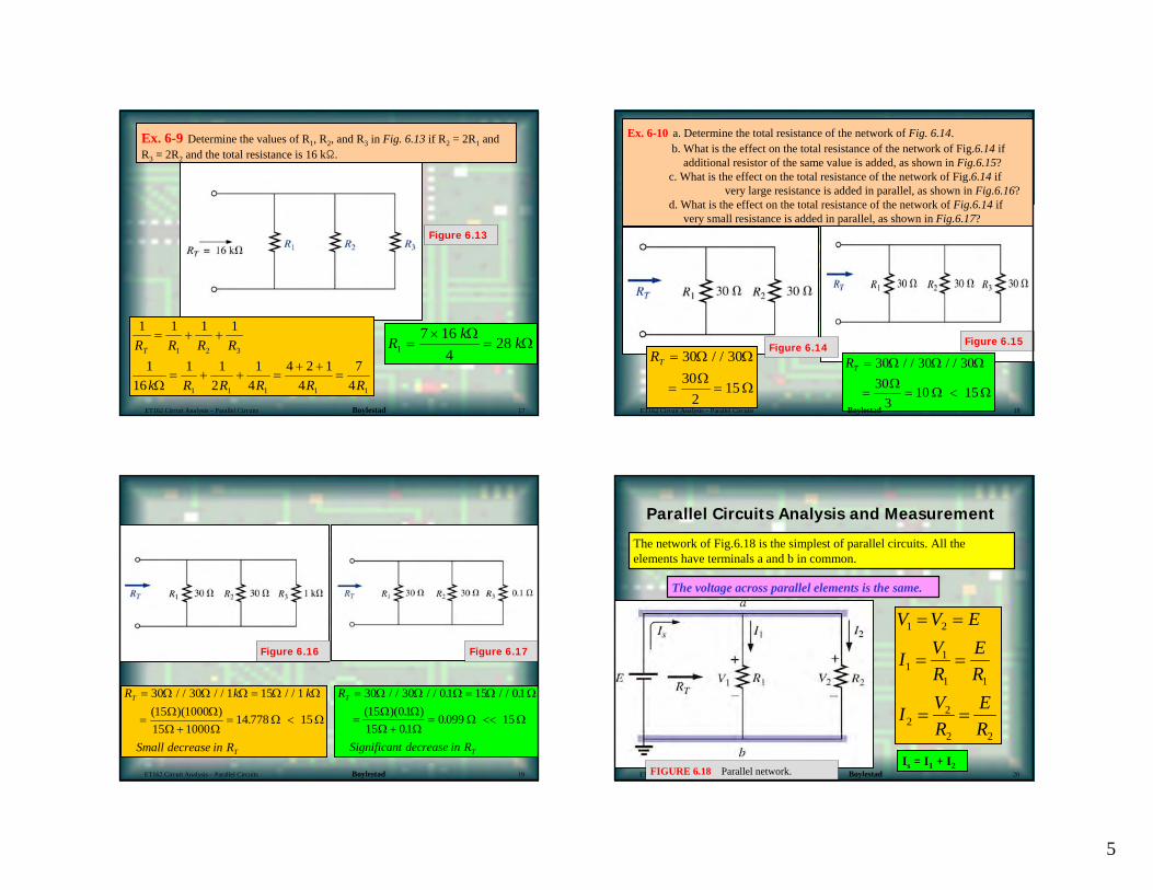
Ex. 6-9 Determine the values of R1, R2, and R3 in Fig. 6.13 if R2 = 2R1 and R3 = 2R2 and the total resistance is 16 kΩ.
1 1 1 1
116
1 12
14
4 2 14
74
1 2 3
1 1 1 1 1
R R R R
k R R R R R
T
= + +
= + + =+ +
=Ω
Rk
k17 16
428=
×=
ΩΩ
Figure 6.13
ET162 Circuit Analysis – Parallel Circuits Boylestad 17
RT =
= =
30 3030
215
Ω ΩΩ
Ω
/ /
Ex. 6-10 a. Determine the total resistance of the network of Fig. 6.14.b. What is the effect on the total resistance of the network of Fig.6.14 if
additional resistor of the same value is added, as shown in Fig.6.15?c. What is the effect on the total resistance of the network of Fig.6.14 if
very large resistance is added in parallel, as shown in Fig.6.16?d. What is the effect on the total resistance of the network of Fig.6.14 if
very small resistance is added in parallel, as shown in Fig.6.17?
RT =
= = <
30 30 3030
310 15
Ω Ω ΩΩ
Ω Ω
/ / / /Figure 6.14 Figure 6.15
ET162 Circuit Analysis – Parallel Circuits Boylestad 18
R k k
Small decrease in R
T
T
= =
=+
= <
30 30 1 15 115 100015 1000
14 778 15
Ω Ω Ω Ω ΩΩ ΩΩ Ω
Ω Ω
/ / / / / /( )( )
.
R
Significant decrease in R
T
T
= =
=+
= <<
30 30 01 15 0115 0115 01
0 099 15
Ω Ω Ω Ω ΩΩ ΩΩ Ω
Ω Ω
/ / / / . / / .( )( . )
..
Figure 6.16 Figure 6.17
ET162 Circuit Analysis – Parallel Circuits Boylestad 19 ET162 Circuit Analysis – Parallel Circuits II Boylestad 20
Parallel Circuits Analysis and Measurement
The network of Fig.6.18 is the simplest of parallel circuits. All the elements have terminals a and b in common.
FIGURE 6.18 Parallel network.
The voltage across parallel elements is the same.
22
22
11
11
21
RE
RVI
RE
RVI
EVV
==
==
==
Is = I1 + I2
6
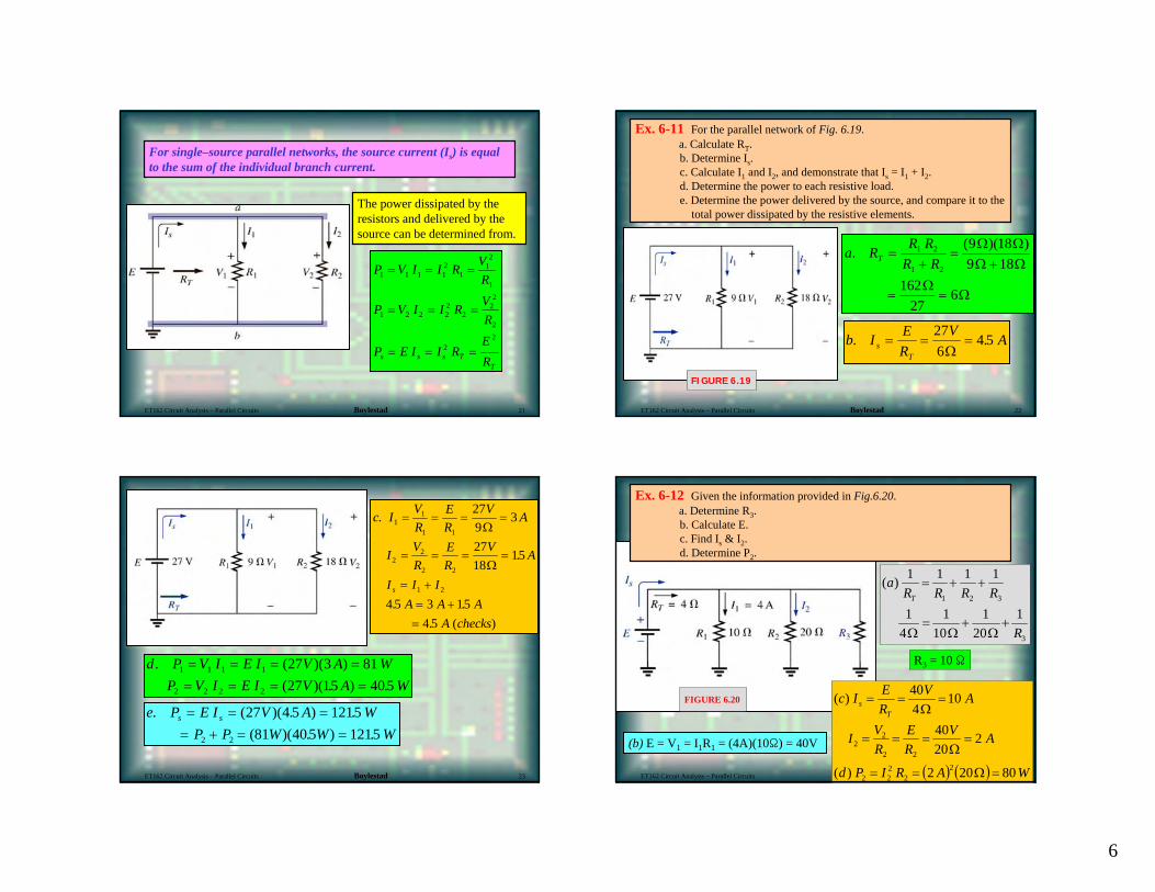
For single–source parallel networks, the source current (Is) is equal to the sum of the individual branch current.
P V I I RVR
P V I I RVR
P E I I RERs s s T
T
1 1 1 12
112
1
1 2 2 22
222
2
22
= = =
= = =
= = =
The power dissipated by the resistors and delivered by the source can be determined from.
ET162 Circuit Analysis – Parallel Circuits Boylestad 21
Ex. 6-11 For the parallel network of Fig. 6.19.a. Calculate RT.b. Determine Is.c. Calculate I1 and I2, and demonstrate that Is = I1 + I2.d. Determine the power to each resistive load.e. Determine the power delivered by the source, and compare it to the
total power dissipated by the resistive elements.
a RR R
R RT.( )( )
=+
=+
= =
1 2
1 2
9 189 18
16227
6
Ω ΩΩ Ω
ΩΩ
FIGURE 6.19
b I ER
VAs
T
. .= = =276
4 5Ω
ET162 Circuit Analysis – Parallel Circuits Boylestad 22
c IVR
ER
VA
IVR
ER
VA
I I IA A A
A checks
s
.
.
. .. ( )
11
1 1
22
2 2
1 2
279
3
2718
15
4 5 3 154 5
= = = =
= = = =
= += +=
Ω
Ω
d P V I E I V A WP V I E I V A W
. ( )( )( )( . ) .
1 1 1 1
2 2 2 2
27 3 8127 15 405
= = = == = = =
e P E I V A WP P W W W
s s. ( )( . ) .(81 )( . ) .
= = == + = =
27 4 5 1215405 12152 2
ET162 Circuit Analysis – Parallel Circuits Boylestad 23 ET162 Circuit Analysis – Parallel Circuits Boylestad 2
FIGURE 6.20
Ex. 6-12 Given the information provided in Fig.6.20.a. Determine R3.b. Calculate E.c. Find Is & I2.d. Determine P2.
3
321
120
110
141
1111)(
R
RRRRa
T
+Ω
+Ω
=Ω
++=
R3 = 10 Ω
(b) E = V1 = I1R1 = (4A)(10Ω) = 40V
( ) ( ) WARIPd
AVRE
RVI
AVREIc
Ts
80202)(
22040
10440)(
22
222
22
22
=Ω==
=Ω
===
=Ω
==
7
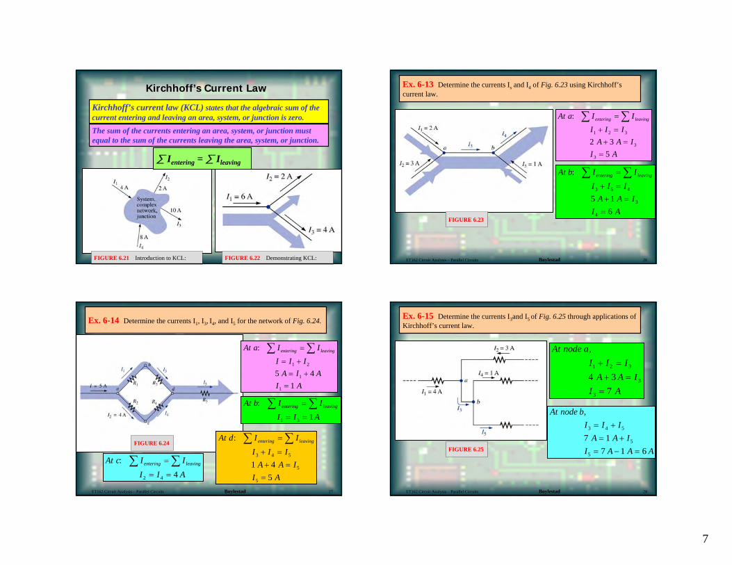
KirchhoffKirchhoff’’ss Current LawCurrent Law
∑ Ientering = ∑ Ileaving
Kirchhoff’s current law (KCL) states that the algebraic sum of the current entering and leaving an area, system, or junction is zero.
FIGURE 6.21 Introduction to KCL:
The sum of the currents entering an area, system, or junction must equal to the sum of the currents leaving the area, system, or junction.
FIGURE 6.22 Demonstrating KCL:
Ex. 6-13 Determine the currents Is and I4 of Fig. 6.23 using Kirchhoff’scurrent law.
At a I I
I I IA A I
I A
entering leaving: ∑ ∑=+ =+ ==
1 2 3
3
3
2 35
At b I I
I I IA A I
I A
entering leaving: ∑ ∑=+ =+ ==
3 5 4
3
4
5 16
FIGURE 6.23
ET162 Circuit Analysis – Parallel Circuits Boylestad 26
Ex. 6-14 Determine the currents I1, I3, I4, and I5 for the network of Fig. 6.24.
At d I I
I I IA A I
I A
entering leaving: ∑ ∑=+ =+ ==
3 4 5
5
5
1 45
At b I I
I I Aentering leaving: ∑ ∑== =1 3 1
At a I I
I I IA I A
I A
entering leaving: ∑ ∑== += +
=
1 2
1
1
5 41
At c I I
I I Aentering leaving: ∑ ∑== =2 4 4
FIGURE 6.24
ET162 Circuit Analysis – Parallel Circuits Boylestad 27
Ex. 6-15 Determine the currents I3and I5 of Fig. 6.25 through applications ofKirchhoff’s current law.
At node aI I I
A A II A
,
1 2 3
3
3
4 37
+ =+ ==
At node bI I I
A A II A A A
,
3 4 5
5
5
7 17 1 6
= += +
= − =FIGURE 6.25
ET162 Circuit Analysis – Parallel Circuits Boylestad 28
8
FIGURE 6.26
Ex. 6-16 Find the magnitude and direction of the currents I3, I4, I6, and I7 for the network of Fig.6.26.
I7 = I1 = 10 AI3 = 2 AI4 = 4 AI6 = 2 A
ET162 Circuit Analysis – Parallel Circuits Boylestad 29
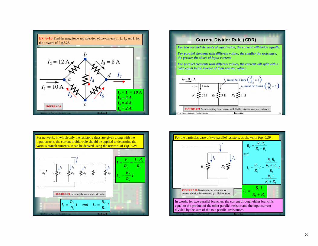
Current Divider Rule (CDR)For two parallel elements of equal value, the current will divide equally.
For parallel elements with different values, the smaller the resistance, the greater the share of input current.
For parallel elements with different values, the current will split with a ratio equal to the inverse of their resistor values.
FIGURE 6.27 Demonstrating how current will divide between unequal resistors.ET162 Circuit Analysis – Parallel Circuits Boylestad 30
I VR
I RR
I RR
I
T
x x
T
xT
x
= =
=
IRR
I and IRR
IT T1
12
2
= =
FIGURE 6.28 Deriving the current divider rule.
For networks in which only the resistor values are given along with the input current, the current divider rule should be applied to determine the various branch currents. It can be derived using the network of Fig. 6.28.
ET162 Circuit Analysis – Parallel Circuits Boylestad 31
RR R
R Rand
I RR
I
R RR R
RI
R IR R
T
T
=+
= =+
=+
1 2
1 2
11
1 2
1 2
1
2
1 2
For the particular case of two parallel resistors, as shown in Fig. 6.29.
I R IR R2
1
1 2
=+
In words, for two parallel branches, the current through either branch is equal to the product of the other parallel resistor and the input current divided by the sum of the two parallel resistances.
FIGURE 6.29 Developing an equation for current division between two parallel resistors.
ET162 Circuit Analysis – Parallel Circuits II Boylestad 32
9
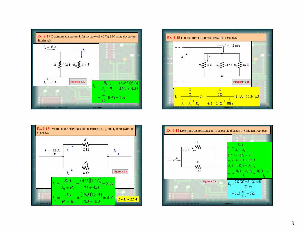
Ex. 6-17 Determine the current I2 for the network of Fig.6.30 using the current divider rule.
IR I
R Rk A
k k
A A
s2
1
1 2
4 64 8
412
6 2
=+
=+
= =
( )( )
( )
ΩΩ Ω
FIGURE 6.30
ET162 Circuit Analysis – Parallel Circuits Boylestad 33
Ex. 6-18 Find the current I1 for the network of Fig.6.31.
FIGURE 6.31
mAmAI
RRR
RI T 54.3042
481
241
61
61
111
1
321
11 =
Ω+
Ω+
Ω
Ω=++
=
ET162 Circuit Analysis – Parallel Circuits Boylestad 34
ET162 Circuit Analysis – Parallel Circuits II Floyd 35
Figure 6.32
Ex. 6-19 Determine the magnitude of the currents I1, I2, and I3 for network of Fig. 6.32.
( )( )
( )( ) AARRIRI
AARRIRI
442
122
842
124
21
12
21
21
=Ω+Ω
Ω=
+=
=Ω+Ω
Ω=
+=
I = I3 = 12 A
Ex. 6-19 Determine the resistance R1 to effect the division of current in Fig. 6.33.
RmA mA
mA17 27 21
21
7 621
2
=−
= ⎛⎝⎜
⎞⎠⎟=
Ω
Ω Ω
( )
IR I
R RR R I R I
R I R I R IR I R I R I
R R I R II
R I II
12
1 2
1 2 1 2
1 1 2 1 2
1 1 2 2 1
12 2 1
1
2 1
1
=+
+ =+ == −
=−
=−
( )
( )
Figure 6.32
ET162 Circuit Analysis – Parallel Circuits Boylestad 36
10
ET162 Circuit Analysis – Parallel Circuits II Floyd 37
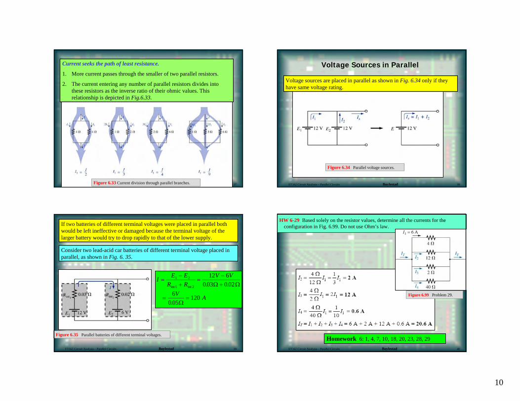
Current seeks the path of least resistance.
1. More current passes through the smaller of two parallel resistors.
2. The current entering any number of parallel resistors divides into these resistors as the inverse ratio of their ohmic values. This relationship is depicted in Fig.6.33.
Figure 6.33 Current division through parallel branches.
Voltage Sources in Parallel
Voltage sources are placed in parallel as shown in Fig. 6.34 only if they have same voltage rating.
Figure 6.34 Parallel voltage sources.
ET162 Circuit Analysis – Parallel Circuits Boylestad 38
If two batteries of different terminal voltages were placed in parallel both would be left ineffective or damaged because the terminal voltage of the larger battery would try to drop rapidly to that of the lower supply.
Consider two lead-acid car batteries of different terminal voltage placed in parallel, as shown in Fig. 6. 35.
IE E
R RV V
VA
=−+
=−+
= =
1 2
1 2
12 60 03 0 02
60 05
120
int int . .
.
Ω Ω
Ω
Figure 6.35 Parallel batteries of different terminal voltages.
ET162 Circuit Analysis – Parallel Circuits Boylestad 39
HW 6-29 Based solely on the resistor values, determine all the currents for the configuration in Fig. 6.99. Do not use Ohm’s law.
Homework 6: 1, 4, 7, 10, 18, 20, 23, 28, 29
Figure 6.99 Problem 29.
ET162 Circuit Analysis – Parallel Circuits Boylestad 40
1
Series and Parallel Networks
EET1122/ET162 Circuit Analysis
Electrical and Telecommunications Engineering Technology Department
Professor JangPrepared by textbook based on “Introduction to Circuit Analysis”
by Robert Boylestad, Prentice Hall, 10th edition.
AcknowledgementAcknowledgement
I want to express my gratitude to Prentice Hall giving me the permission to use instructor’s material for developing this module. I would like to thank the Department of Electrical and Telecommunications Engineering Technology of NYCCT for giving me support to commence and complete this module. I hope this module is helpful to enhance our students’academic performance.
Sunghoon Jang
OUTLINESOUTLINES
Introduction to Series-Parallel Networks
Reduce and Return Approach
Block Diagram Approach
Descriptive Examples
Ladder Networks
ET162 Circuit Analysis – Series and Parallel Networks Boylestad 2
Key Words: Series-Parallel Network, Block Diagram, Ladder Network FIGURE 7.1 Introducing the reduce and return approach.
Series-Parallel Networks –Reduce and Return Approach
Series-parallel networks are networks that contain both series and parallel circuit configurations
For many single-source, series-parallel networks, the analysis is one that works back to the source, determines the source current, and then finds its way to the desired unknown.
ET162 Circuit Analysis – Series and parallel networks Boylestad 3
2
FIGURE 7.2 Introducing the block diagram approach.
Series-Parallel NetworksBlock Diagram Approach
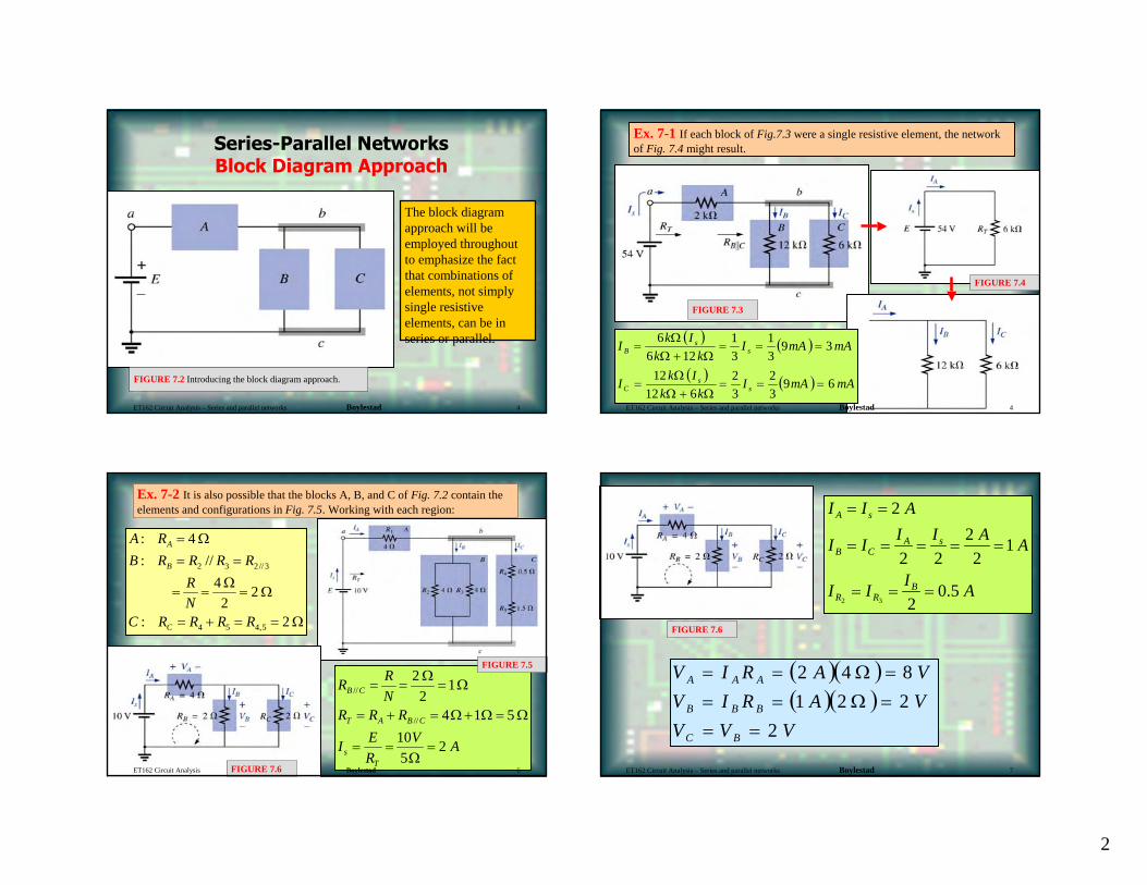
The block diagram approach will be employed throughout to emphasize the fact that combinations of elements, not simply single resistive elements, can be in series or parallel.
ET162 Circuit Analysis – Series and parallel networks Boylestad 4
FIGURE 7.3
Ex. 7-1 If each block of Fig.7.3 were a single resistive element, the network of Fig. 7.4 might result.
( ) ( )
( ) ( ) mAmAIkk
IkI
mAmAIkk
IkI
ss
C
ss
B
6932
32
61212
3931
31
1266
===Ω+Ω
Ω=
===Ω+Ω
Ω=
FIGURE 7.4
ET162 Circuit Analysis – Series and parallel networks Boylestad 4
AVREI
RRRNRR
Ts
CBAT
CB
2510
514
12
2
//
//
=Ω
==
Ω=Ω+Ω=+=
Ω=Ω
==
Ex. 7-2 It is also possible that the blocks A, B, and C of Fig. 7.2 contain the elements and configurations in Fig. 7.5. Working with each region:
Ω==+=
Ω=Ω
==
==Ω=
2:
22
4//:
4:
5,454
3//232
RRRRCNR
RRRRBRA
C
B
A
FIGURE 7.5
FIGURE 7.6ET162 Circuit Analysis Boylestad 6
AIII
AAIIII
AII
BRR
sACB
sA
5.02
12
222
2
32===
=====
==
( )( )( )( )
VVVVARIVVARIV
BC
BBB
AAA
2221842
===Ω===Ω==
ET162 Circuit Analysis – Series and parallel networks Boylestad 7
FIGURE 7.6
3
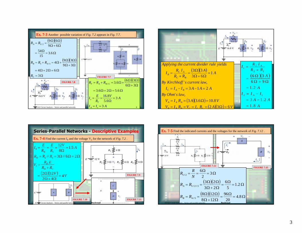
Ex. 7-3 Another possible variation of Fig. 7.2 appears in Fig. 7.7.
( )( )
( )( )
Ω=Ω=Ω+Ω=
Ω+ΩΩΩ
+Ω=+=
Ω=Ω
=
Ω+ΩΩΩ
==
3624
39394
6.315
546969
5//43
2//1
C
B
A
R
RRR
RR
( )( )
AII
AVREI
RRR
sA
Ts
CBAT
3
36.58.16
6.526.336366.3//
==
=Ω
==
Ω=Ω+Ω=Ω+ΩΩΩ
+Ω=+=
FIGURE 7.7
FIGURE 7.8
ET162 Circuit Analysis – Series and parallel networks 8
( )( )
( )( )( )( ) VARIVRIV
VARIVlawsOhmBy
AAAIIIlawcurrentsKirchhoffBy
AARR
IRI
yieldsruledividercurrenttheApplying
CCCBBB
AAA
BAC
BC
ACB
6328.106.33
,'213,'
16333
=Ω=====Ω==
=−=−=
=Ω+Ω
Ω=
+= ( )( )
AAA
IIIA
ARR
IRI
A
A
8.12.13
2.19636
12
12
21
=−=−=
=Ω+Ω
Ω=
+=
Series-Parallel Networks - Descriptive Examples
Ex. 7-4 Find the current I4 and the voltage V2 for the network of Fig. 7.2 .
( )( ) VVRRERV
RRR
AVRE
REI
CD
D
D
B
442
122
26//3//
5.1812
2
32
44
=Ω+Ω
Ω=
+=
Ω=ΩΩ==
=Ω
===
FIGURE 7.9
FIGURE 7.10 FIGURE 7.11ET162 Circuit Analysis – Series and parallel networks Boylestad 10
Ex. 7-5 Find the indicated currents and the voltages for the network of Fig. 7.12 .
FIGURE 7.13
( )( )
( )( )Ω=
Ω=
Ω+ΩΩΩ
==
Ω=Ω
=Ω+ΩΩΩ
==
Ω=Ω
==
8.420
96128128
2.15
62323
32
6
5//4
3//2//1
2//1
RR
RR
NRR
B
A
FIGURE 7.12
ET162 Circuit Analysis – Series and parallel networks Boylestad 11
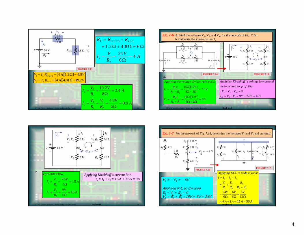
4
ET162 Circuit Analysis – Series and parallel networks Boylestad 12
AVREI
RRR
Ts
T
4624
68.42.15//43//2//1
=Ω
==
Ω=Ω+Ω=+=
( )( )( )( ) VARIV
VARIV
s
s
2.198.448.42.14
5//42
3//2//11
=Ω===Ω==
FIGURE 7.13
AVRV
RVI
AVRVI
8.068.4
4.28
2.19
2
1
2
22
4
54
=Ω
===
=Ω
==
Ex. 7-6 a. Find the voltages V1, V2, and Vab for the network of Fig. 7.14.b. Calculate the source current Is.
( )( )
( )( )
Applying the voltage divider rule yields
VR E
R RV
V
VR E
R RV
V
11
1 2
33
3 4
5 125 3
7 5
6 126 2
9
=+
=+
=
=+
=+
=
ΩΩ Ω
ΩΩ Ω
.
Applying Kirchhoff s voltage law aroundthe indicated loop of Fig
V V VV V V V V V
ab
ab
'.
. .− + − =
= − = − =1 3
3 1
09 7 5 15
FIGURE 7.14a.
FIGURE 7.15
ET162 Circuit Analysis – Series and parallel networks Boylestad 13
b. By Ohm s law
IVR
VA
I VR
V A
' ,.
.
.
11
1
33
3
7 55
15
96
15
= = =
= = =
Ω
Ω
Applying Kirchhoff’s current law,Is = I1 + I3 = 1.5A + 1.5A = 3A
ET162 Circuit Analysis – Series and parallel networks Boylestad 14
Ex. 7-7 For the network of Fig. 7.16, determine the voltages V1 and V2 and current I.
FIGURE 7.17FIGURE 7.16
V2 = – E1 = – 6V
Applying KVL to the loopE1 – V1 + E2 = 0V1 = E2 + E1 =18V + 6V = 24V
Applying KCL to node a yieldsI I I I
VR
ER
ER R
V V V
A A A A
= + +
= + ++
= + +
= + + =
1 2 3
1
1
1
4
1
2 3
246
66
612
4 1 05 55Ω Ω Ω
. .ET162 Circuit Analysis – Series and parallel networks Boylestad 15
5
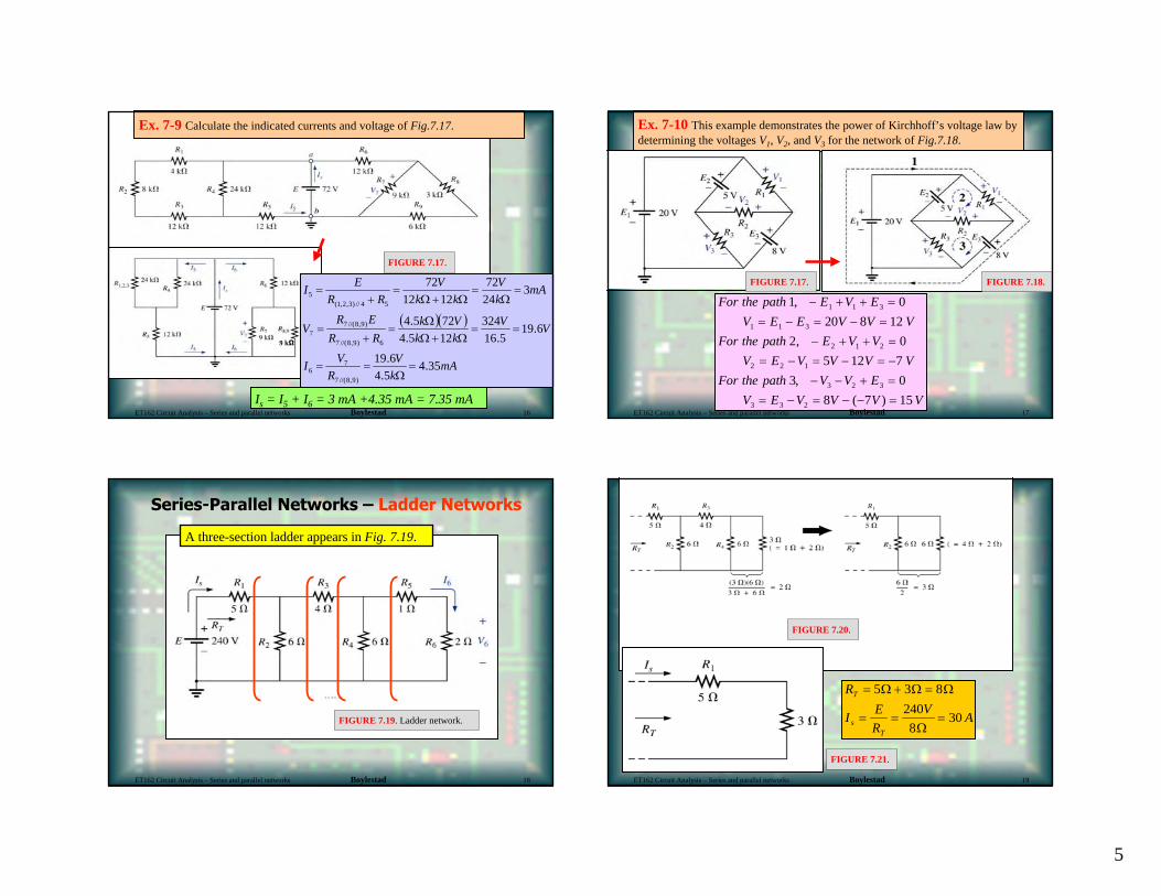
Ex. 7-9 Calculate the indicated currents and voltage of Fig.7.17.
FIGURE 7.17.
( )( )
mAkV
RVI
VVkkVk
RRER
V
mAkV
kkV
RREI
35.45.46.19
6.195.16
324125.4725.4
32472
121272
)9,8//(7
76
6)9,8//(7
)9,8//(77
54//)3,2,1(5
=Ω
==
==Ω+Ω
Ω=
+=
=Ω
=Ω+Ω
=+
=
Is = I5 + I6 = 3 mA +4.35 mA = 7.35 mA
9 kΩ
ET162 Circuit Analysis – Series and parallel networks Boylestad 16
Ex. 7-10 This example demonstrates the power of Kirchhoff’s voltage law by determining the voltages V1, V2, and V3 for the network of Fig.7.18.
FIGURE 7.17.
For the path E V EV E E V V V
For the path E V VV E V V V V
For the path V V EV E V V V V
1 020 8 12
2 05 12 7
3 08 7 15
1 1 3
1 1 3
2 1 2
2 2 1
3 2 3
3 3 2
,
,
,( )
− + + == − = − =
− + + == − = − = −
− − + == − = − − =
FIGURE 7.18.
ET162 Circuit Analysis – Series and parallel networks Boylestad 17
Series-Parallel Networks – Ladder Networks
A three-section ladder appears in Fig. 7.19.
FIGURE 7.19. Ladder network.
ET162 Circuit Analysis – Series and parallel networks Boylestad 18
R
I ER
VA
T
sT
= + =
= = =
5 3 82408
30
Ω Ω Ω
Ω
FIGURE 7.20.
FIGURE 7.21.
ET162 Circuit Analysis – Series and parallel networks Boylestad 19
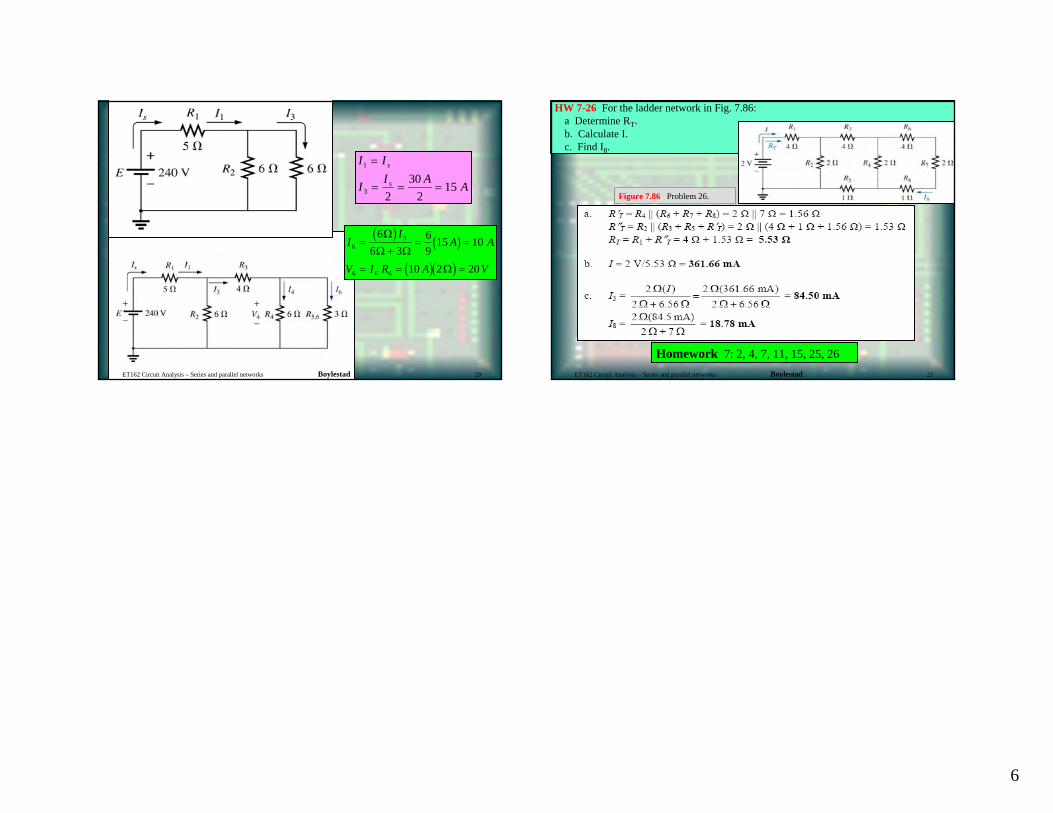
6
I I
I I A A
s
s
1
3 230
215
=
= = =
( ) ( )
( )( )
II
A A
V I R A V
63
6 6 6
66 3
69
15 10
10 2 20
=+
= =
= = =
ΩΩ Ω
Ω
ET162 Circuit Analysis – Series and parallel networks Boylestad 20
HW 7-26 For the ladder network in Fig. 7.86:a Determine RT.b. Calculate I.c. Find I8.
Homework 7: 2, 4, 7, 11, 15, 25, 26
Figure 7.86 Problem 26.
ET162 Circuit Analysis – Series and parallel networks Boylestad 21

1
Methods of Analysis
EET/1122/ET162 Circuit Analysis
Electrical and Telecommunications Engineering Technology Department
Professor JangPrepared by textbook based on “Introduction to Circuit Analysis”
by Robert Boylestad, Prentice Hall, 10th edition.
AcknowledgementAcknowledgement
I want to express my gratitude to Prentice Hall giving me the permission to use instructor’s material for developing this module. I would like to thank the Department of Electrical and Telecommunications Engineering Technology of NYCCT for giving me support to commence and complete this module. I hope this module is helpful to enhance our students’ academic performance.
Sunghoon Jang
OUTLINESOUTLINES
Introduction to Method AnalysisCurrent Sources
Source Conversions
Current Sources in SeriesBranch Current Analysis
Mesh & Super Mesh Analysis
Nodal & Super Nodal Analysis
ET162 Circuit Analysis – Methods of Analysis Boylestad 2
Key Words: Current Source, Source Conversion, Branch Current, Mesh Analysis, Nodal Analysis
The circuits described in the previous chapters had only one source or two or more sources in series or parallel present. The step-by-step procedure outlined in those chapters cannot be applied if the sources are not in series or parallel.
Methods of analysis have been developed that allow us to approach, in a systematic manner, a network with any number of sources in any arrangement. Branch-current analysis, mesh analysis, and nodal analysis will be discussed in detail in this chapter.
ET162 Circuit Analysis – Methods of Analysis Boylestad 3
Introduction to Methods of Analysis
2
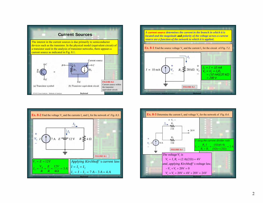
FIGURE 8.1Current source within the transistor equivalent circuit.
Current Sources
The interest in the current sources is due primarily to semiconductor devices such as the transistor. In the physical model (equivalent circuit) of a transistor used in the analysis of transistor networks, there appears a current source as indicated in Fig. 8.1.
ET162 Circuit Analysis – Methods of Analysis Boylestad 4
Ex. 8-1 Find the source voltage Vs and the current I1 for the circuit of Fig. 7.2.
FIGURE 8.2
A current source determines the current in the branch in which it is located and the magnitude and polarity of the voltage across a current source are a function of the network to which it is applied.
I1 = I = 10 mAVs = V1 = I1R1
= (10 mA)(20 kΩ)= 200 V
ET162 Circuit Analysis – Methods of Analysis Boylestad 5
V E V
I VR
ER
V A
s
R
= =
= = = =
12124
32 Ω
Ex. 8-2 Find the voltage Vs and the currents I1 and I2 for the network of Fig. 8.3.
FIGURE 8.3
Applying Kirchhoff s current lawI I II I I A A A
' := += − = − =
1 2
1 2 7 3 4ET162 Circuit Analysis – Methods of Analysis Boylestad 6
U g the current divider rule
IR I
R RA
A
sin :( )( )
( ) ( )12
2 1
1 61 2
2=+
=+
=ΩΩ Ω
Ex. 8-3 Determine the current I1 and voltage Vs for the network of Fig. 8.4.
FIGURE 8.4
The voltage V isV I R A V
and applying Kirchhoff s voltage lawV V V
V V V V V Vs
s
1
1 1 1
1
1
2 2 4
20 020 4 20 24
= = =
− + + == + = + =
( )( ), ' ,
Ω
ET162 Circuit Analysis – Methods of Analysis Boylestad 7
3
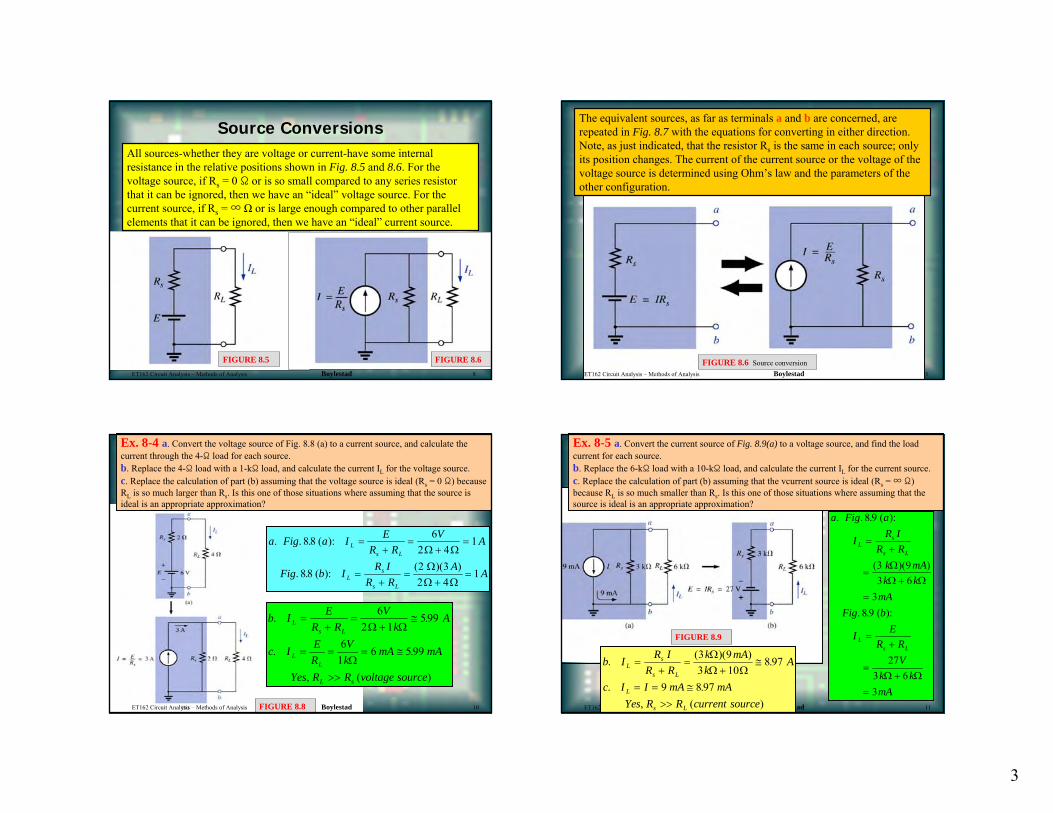
Source Conversions
FIGURE 8.6FIGURE 8.5
All sources-whether they are voltage or current-have some internal resistance in the relative positions shown in Fig. 8.5 and 8.6. For the voltage source, if Rs = 0 Ω or is so small compared to any series resistor that it can be ignored, then we have an “ideal” voltage source. For the current source, if Rs = ∞ Ω or is large enough compared to other parallel elements that it can be ignored, then we have an “ideal” current source.
ET162 Circuit Analysis – Methods of Analysis Boylestad 8
The equivalent sources, as far as terminals a and b are concerned, are repeated in Fig. 8.7 with the equations for converting in either direction. Note, as just indicated, that the resistor Rs is the same in each source; only its position changes. The current of the current source or the voltage of the voltage source is determined using Ohm’s law and the parameters of the other configuration.
FIGURE 8.6 Source conversionET162 Circuit Analysis – Methods of Analysis Boylestad 3
a Fig a I ER R
VA
Fig b I R IR R
A A
Ls L
Ls
s L
. . . ( ):
. . ( ): ( )( )
886
2 41
88 2 32 4
1
=+
=+
=
=+
=+
=
Ω ΩΩΩ Ω
Ex. 8-4 a. Convert the voltage source of Fig. 8.8 (a) to a current source, and calculate the current through the 4-Ω load for each source.b. Replace the 4-Ω load with a 1-kΩ load, and calculate the current IL for the voltage source.c. Replace the calculation of part (b) assuming that the voltage source is ideal (Rs = 0 Ω) because RL is so much larger than Rs. Is this one of those situations where assuming that the source is ideal is an appropriate approximation?
FIGURE 8.8
b I ER R
Vk
A
c I ER
Vk
mA mA
Yes R R voltage source
Ls L
LL
L s
. .
. .
, ( )
=+
=+
≅
= = = ≅
>>
62 1
599
61
6 599
Ω Ω
Ω
ET162 Circuit Analysis – Methods of Analysis Boylestad 10 ET162 Circuit Analysis – Methods of Analysis Boylestad 11
a Fig a
IR I
R Rk mAk k
mAFig b
I ER R
Vk kmA
Ls
s L
Ls L
. . . ( ):
( )( )
. . ( ):
8 9
3 93 6
38 9
273 63
=+
=+
=
=+
=+
=
ΩΩ Ω
Ω Ω
Ex. 8-5 a. Convert the current source of Fig. 8.9(a) to a voltage source, and find the load current for each source.b. Replace the 6-kΩ load with a 10-kΩ load, and calculate the current IL for the current source.c. Replace the calculation of part (b) assuming that the vcurrent source is ideal (Rs = ∞Ω) because RL is so much smaller than Rs. Is this one of those situations where assuming that the source is ideal is an appropriate approximation?
b I R IR R
k mAk
A
c I I mA mAYes R R current source
Ls
s L
L
s L
. ( )( ) .
. ., ( )
=+
=+
≅
= = ≅>>
3 93 10
8 97
9 8 97
ΩΩ Ω
FIGURE 8.9
4
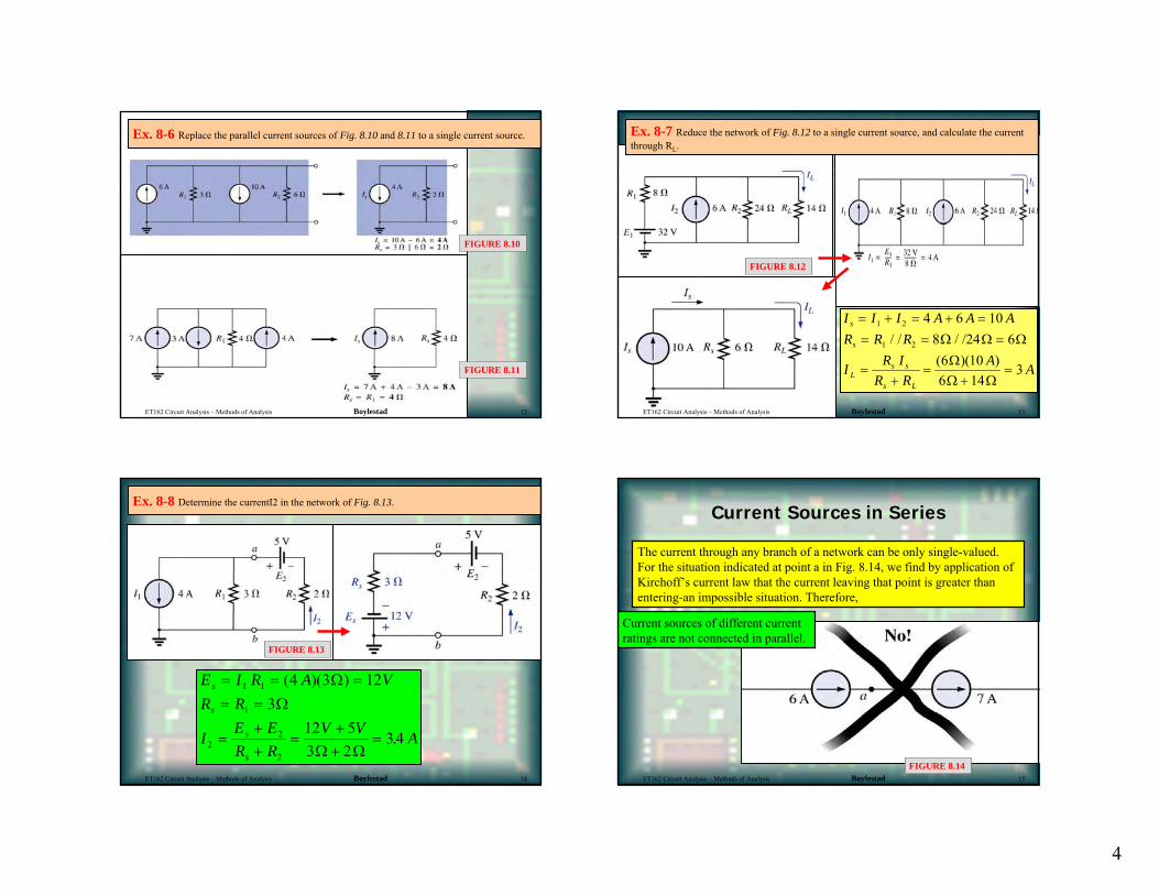
Ex. 8-6 Replace the parallel current sources of Fig. 8.10 and 8.11 to a single current source.
FIGURE 8.11
FIGURE 8.10
ET162 Circuit Analysis – Methods of Analysis Boylestad 12
FIGURE 8.12
Ex. 8-7 Reduce the network of Fig. 8.12 to a single current source, and calculate the current through RL.
I I I A A AR R R
I R IR R
A A
s
s
Ls s
s L
= + = + == = =
=+
=+
=
1 2
1 2
4 6 108 6
6 106 14
3
/ / / /24( )( )Ω Ω ΩΩΩ Ω
ET162 Circuit Analysis – Methods of Analysis Boylestad 13
Ex. 8-8 Determine the currentI2 in the network of Fig. 8.13.
FIGURE 8.13
E I R A VR R
IE ER R
V VA
s
s
s
s
= = == =
=++
=++
=
1 1
1
22
2
4 3 123
12 53 2
34
( )( )
.
ΩΩ
Ω Ω
ET162 Circuit Analysis – Methods of Analysis Boylestad 14
Current Sources in Series
The current through any branch of a network can be only single-valued. For the situation indicated at point a in Fig. 8.14, we find by application of Kirchoff’s current law that the current leaving that point is greater thanentering-an impossible situation. Therefore,
Current sources of different current ratings are not connected in parallel.
FIGURE 8.14ET162 Circuit Analysis – Methods of Analysis Boylestad 15
5
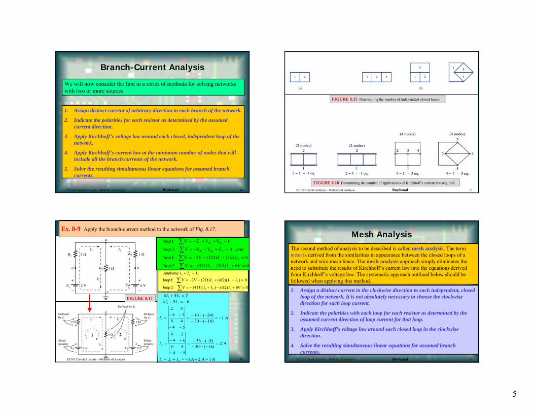
Branch-Current Analysis
We will now consider the first in a series of methods for solving networks with two or more sources.
1. Assign distinct current of arbitrary direction to each branch of the network.
2. Indicate the polarities for each resistor as determined by the assumed current direction.
3. Apply Kirchhoff’s voltage law around each closed, independent loop of the network.
4. Apply Kirchhoff’s current law at the minimum number of nodes that will include all the branch currents of the network.
5. Solve the resulting simultaneous linear equations for assumed branch currents.
ET162 Circuit Analysis – Methods of Analysis Boylestad 16
FIGURE 8.15 Determining the number of independent closed loops.
FIGURE 8.16 Determining the number of applications of Kirchhoff’s current law required.
ET162 Circuit Analysis – Methods of Analysis Boylestad 17
loop V E V V
loop V V V E and
loop V V I I
loop V I I V
R R
R R
1 0
2 0
1 2 2 4 0
2 4 1 6 0
1
2
1 3
3 2
1 3
3 2
:
:
: ( ) ( )
: ( ) ( )
∑∑∑∑
= − + + =
= − − + =
= − + + =
= − − + =
Ω Ω
Ω Ω
Ex. 8-9 Apply the branch-current method to the network of Fig. 8.17.
FIGURE 8.17
Applying I I I
loop V V I I I
loop V I I I V
1 2 3
1 1 2
1 2 2
1 2 2 4 0
2 4 1 6 0
+ =
= − + + + =
= − + − + =
∑∑
: ( ) ( )( )
: ( )( ) ( )
Ω Ω
Ω Ω
6 4 24 5 6
2 46 5
6 44 5
10 2430 16
1
6 24 6
6 44 5
36 830 16
2
1 2 1
1 2
1 2
1
2
3 1 2
I II I
I A
I A
I I I A A A
+ =− − = −
=− −
− −
=− − −− − −
= −
=− −
− −
=− − −− − −
=
= + = − + =
( )( )
( )( )
ET162 Circuit Analysis – Methods of Analysis 18
Mesh AnalysisThe second method of analysis to be described is called mesh analysis. The term mesh is derived from the similarities in appearance between the closed loops of a network and wire mesh fence. The mesh-analysis approach simply eliminates the need to substitute the results of Kirchhoff’s current law into the equations derived from Kirchhoff’s voltage law. The systematic approach outlined below should be followed when applying this method.
1. Assign a distinct current in the clockwise direction to each independent, closed loop of the network. It is not absolutely necessary to choose the clockwise direction for each loop current.
2. Indicate the polarities with each loop for each resistor as determined by the assumed current direction of loop current for that loop.
3. Apply Kirchhoff’s voltage law around each closed loop in the clockwise direction.
4. Solve the resulting simultaneous linear equations for assumed branch currents.
ET162 Circuit Analysis – Methods of Analysis Boylestad 19
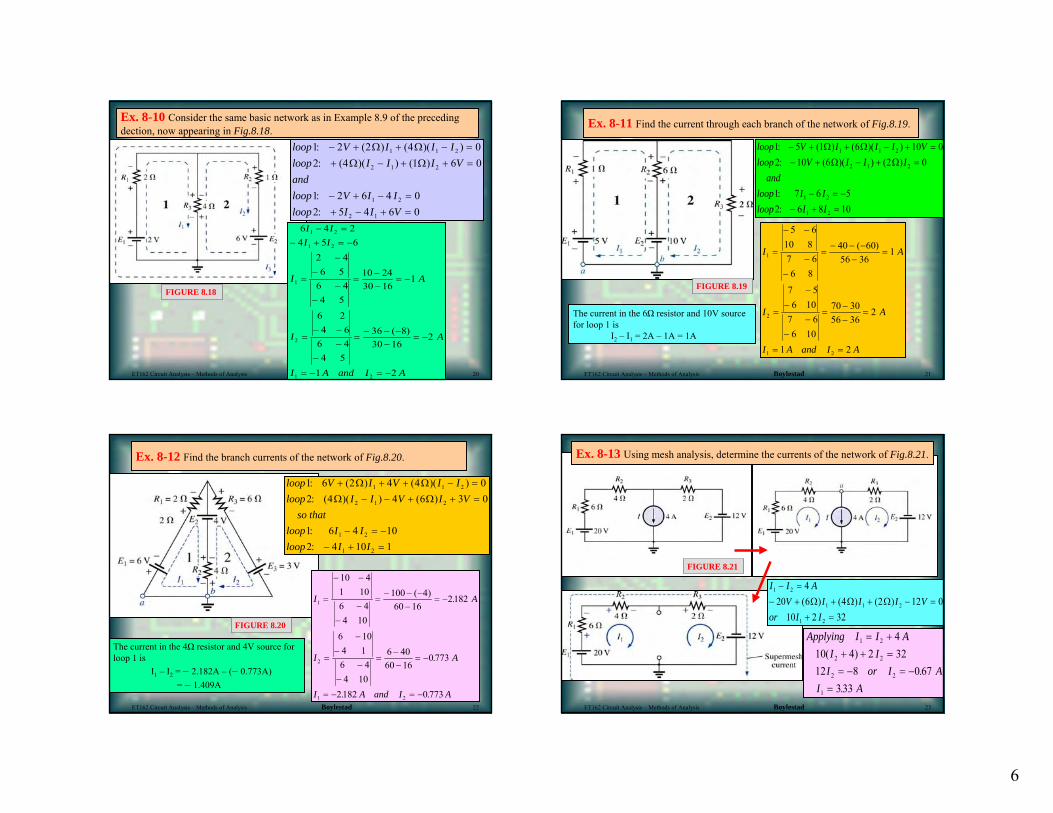
6
loop V I I Iloop I I I Vandloop V I Iloop I I V
1 2 2 4 02 4 1 6 0
1 2 6 4 02 5 4 6 0
1 1 2
2 1 2
1 2
2 1
: ( ) ( )( ): ( )( ) ( )
::
− + + − =+ − + + =
− + − =+ − + =
Ω ΩΩ Ω
Ex. 8-10 Consider the same basic network as in Example 8.9 of the preceding dection, now appearing in Fig.8.18.
ET162 Circuit Analysis – Methods of Analysis Boylestad 20
FIGURE 8.18
6 4 24 5 6
2 46 5
6 44 5
10 2430 16
1
6 24 6
6 44 5
36 830 16
2
1 2
1 2
1 2
1
2
1 2
I II I
I A
I A
I A and I A
− =− + = −
=
−−
−−
=−−
= −
=− −
−−
=− − −
−= −
= − = −
( )
Ex. 8-11 Find the current through each branch of the network of Fig.8.19.
loop V I I I Vloop V I I I
andloop I Iloop I I
1 5 1 6 10 02 10 6 2 0
1 7 6 52 6 8 10
1 1 2
2 1 2
1 2
1 2
: ( ) ( )( ): ( )( ) ( )
::
− + + − + =− + − + =
− = −− + =
Ω ΩΩ Ω
I A
I A
I A and I A
1
2
1 2
5 610 87 66 8
40 6056 36
1
7 56 10
7 66 10
70 3056 36
2
1 2
=
− −
−−
=− − −
−=
=
−−
−−
=−−
=
= =
( )
FIGURE 8.19
The current in the 6Ω resistor and 10V source for loop 1 is
I2 – I1 = 2A – 1A = 1A
ET162 Circuit Analysis – Methods of Analysis Boylestad 21
Ex. 8-12 Find the branch currents of the network of Fig.8.20.
loop V I V I Iloop I I V I V
so thatloop I Iloop I I
1 6 2 4 4 02 4 4 6 3 0
1 6 4 102 4 10 1
1 1 2
2 1 2
1 2
1 2
: ( ) ( )( ): ( )( ) ( )
::
+ + + − =− − + + =
− = −− + =
Ω ΩΩ Ω
I A
I A
I A and I A
1
2
1 2
10 41 106 44 10
100 460 16
2182
6 104 16 44 10
6 4060 16
0 773
2182 0 773
=
− −
−−
=− − −
−= −
=
−−
−−
=−−
= −
= − = −
( ) .
.
. .
FIGURE 8.20
The current in the 4Ω resistor and 4V source for loop 1 is
I1 – I2 = – 2.182A – (– 0.773A)= – 1.409A
ET162 Circuit Analysis – Methods of Analysis Boylestad 22
Applying I I AI I
I or I AI A
1 2
2 2
2 2
1
410 4 2 3212 8 0 67
333
= ++ + == − = −
=
( ).
.
Ex. 8-13 Using mesh analysis, determine the currents of the network of Fig.8.21.
FIGURE 8.21
I I AV I I I V
or I I
1 2
1 1 2
1 2
420 6 4 2 12 0
10 2 32
− =− + + + − =
+ =( ) ( ) ( )Ω Ω Ω
ET162 Circuit Analysis – Methods of Analysis Boylestad 23
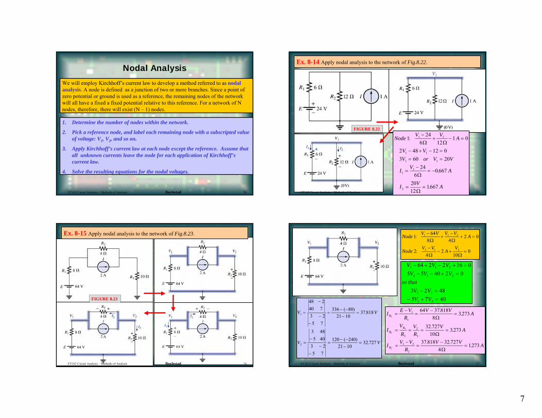
7
Nodal Analysis
We will employ Kirchhoff’s current law to develop a method referred to as nodal analysis. A node is defined as a junction of two or more branches. Since a point of zero potential or ground is used as a reference, the remaining nodes of the network will all have a fixed a fixed potential relative to this reference. For a network of N nodes, therefore, there will exist (N – 1) nodes.
1. Determine the number of nodes within the network.
2. Pick a reference node, and label each remaining node with a subscripted value of voltage: V1, V2, and so on.
3. Apply Kirchhoff’s current law at each node except the reference. Assume that all unknown currents leave the node for each application of Kirchhoff’scurrent law.
4. Solve the resulting equations for the nodal voltages.
ET162 Circuit Analysis – Methods of Analysis Boylestad 24
Ex. 8-14 Apply nodal analysis to the network of Fig.8.22.
FIGURE 8.22
NodeV V
A
V VV or V V
I V A
I V A
124
6 121 0
2 48 12 03 60 20
246
0 667
2012
1667
1 1
1 1
1 1
11
2
:
.
.
−+ − =
− + − == =
=−
= −
= =
Ω Ω
Ω
ΩET162 Circuit Analysis – Methods of Analysis 25
Ex. 8-15 Apply nodal analysis to the network of Fig.8.23.
FIGURE 8.23
ET162 Circuit Analysis – Methods of Analysis Boylestad 26
NodeV V V V
A
NodeV V
AV
164
8 42 0
24
210
0
1 1 2
2 1 2
:
:
−+
−+ =
−− + =
Ω Ω
Ω Ω
V V VV V V
so thatV VV V
1 1 2
2 1 2
1 2
1 2
64 2 2 16 05 5 40 2 0
3 2 485 7 40
− + − + =− − + =
− =− + =
V V
V V
1
2
48 240 73 25 7
336 8021 10
37 818
3 485 40
3 25 7
120 24021 10
32 727
=
−
−−
=− −−
=
=−
−−
=− −−
=
( ) .
( ) .
IE V
RV V
A
IVR
VR
V A
I V VR
V V A
R
RR
R
1`
3
3
2
1
1
3
2
3
1 2
2
64 37 8188
3273
32 72710
3273
37 818 32 7274
1273
=−
=−
=
= = = =
=−
=−
=
..
. .
. . .
`
`
Ω
Ω
Ω
ET162 Circuit Analysis – Methods of Analysis Boylestad 27
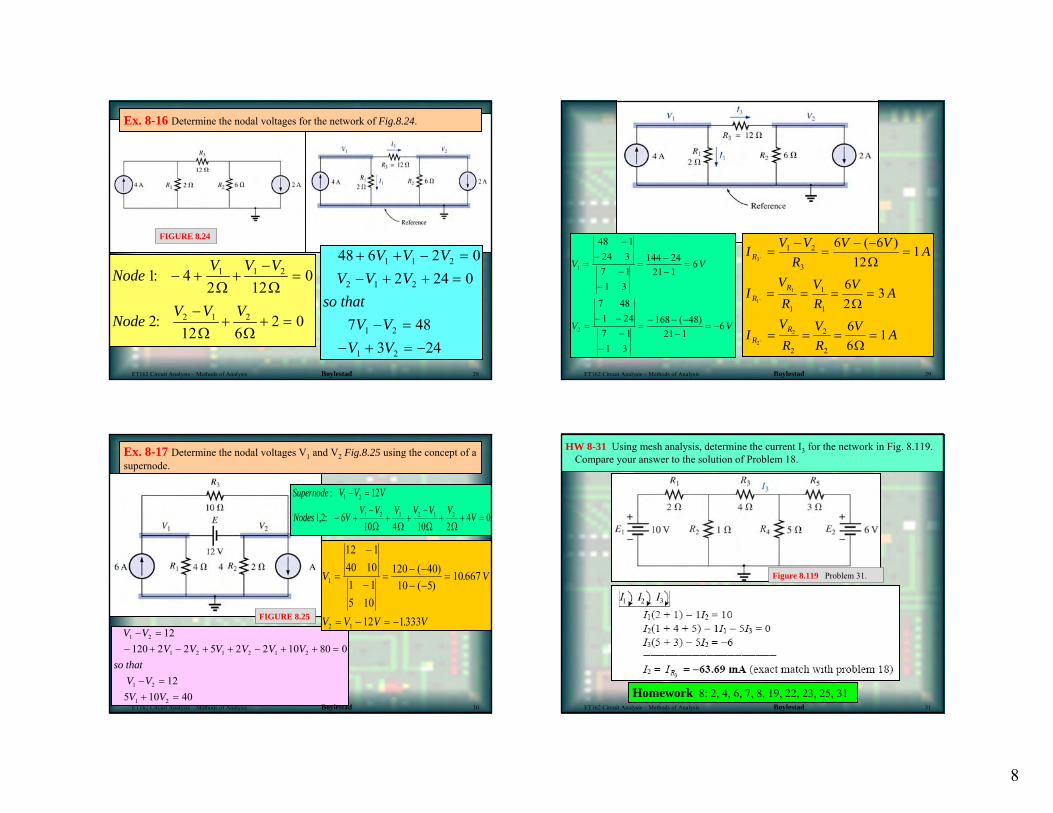
8
NodeV V V
NodeV V V
1 42 12
0
212 6
2 0
1 1 2
2 1 2
:
:
− + +−
=
−+ + =
Ω Ω
Ω Ω
FIGURE 8.24
Ex. 8-16 Determine the nodal voltages for the network of Fig.8.24.
48 6 2 02 24 0
7 483 24
1 1 2
2 1 2
1 2
1 2
+ + − =− + + =
− =− + = −
V V VV V V
so thatV V
V VET162 Circuit Analysis – Methods of Analysis Boylestad 28
V V
V V
1
2
48 124 37 11 3
144 2421 1
6
7 481 247 11 3
168 4821 1
6
=
−−
−−
=−−
=
=− −
−−
=− − −
−= −
( )
I V VR
V V A
IVR
VR
V A
IVR
VR
V A
R
RR
RR
3
1`
1
2
2
1 2
3
1
1
1
2
2
2
6 612
1
62
3
66
1
`
`
( )=
−=
− −=
= = = =
= = = =
Ω
Ω
Ω
ET162 Circuit Analysis – Methods of Analysis Boylestad 29
Ex. 8-17 Determine the nodal voltages V1 and V2 Fig.8.25 using the concept of a supernode.
Supernode V V V
Nodes V V V V V V V V
:
, :
1 2
1 2 1 2 1 2
12
1 2 610 4 10 2
4 0
− =
− +−
+ +−
+ + =Ω Ω Ω Ω
V VV V V V V V
so thatV VV V
1 2
1 2 1 2 1 2
1 2
1 2
12120 2 2 5 2 2 10 80 0
125 10 40
− =− + − + + − + + =
− =+ =
FIGURE 8.25
V V
V V V V
1
2 1
12 140 101 15 10
120 4010 5
10 667
12 1333
=
−
−=
− −− −
=
= − = −
( )( )
.
.
ET162 Circuit Analysis – Methods of Analysis Boylestad 30
HW 8-31 Using mesh analysis, determine the current I3 for the network in Fig. 8.119. Compare your answer to the solution of Problem 18.
Homework 8: 2, 4, 6, 7, 8, 19, 22, 23, 25, 31
Figure 8.119 Problem 31.
ET162 Circuit Analysis – Methods of Analysis Boylestad 31

1
Methods of Analysis
EET1122/ET162 Circuit Analysis
Electrical and Telecommunications Engineering Technology Department
Professor JangPrepared by textbook based on “Introduction to Circuit Analysis”
by Robert Boylestad, Prentice Hall, 10th edition.
AcknowledgementAcknowledgement
I want to express my gratitude to Prentice Hall giving me the permission to use instructor’s material for developing this module. I would like to thank the Department of Electrical and Telecommunications Engineering Technology of NYCCT for giving me support to commence and complete this module. I hope this module is helpful to enhance our students’ academic performance.
Sunghoon Jang
OUTLINESOUTLINES
Introduction to Network Theorems
Superposition
Thevenin’s Theorem
Norton’s Theorem
Maximum Power Transfer Theorem
ET162 Circuit Analysis – Network Theorems Boylestad 2
Key Words: Network Theorem, Superposition, Thevenin, Norton, Maximum Power
This chapter will introduce the important fundamental theorems of network analysis. Included are the superposition,Thevenin’s, Norton’s, and maximum power transfer theorems. We will consider a number of areas of application for each. A through understanding of each theorems will be applied repeatedly in the material to follow.
Introduction to Network Theorems
ET162 Circuit Analysis – Network Theorems Boylestad 3
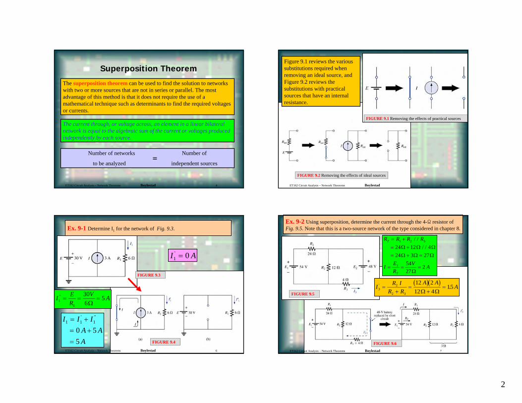
2
Superposition Theorem
The superposition theorem can be used to find the solution to networks with two or more sources that are not in series or parallel. The most advantage of this method is that it does not require the use of a mathematical technique such as determinants to find the required voltages or currents.
The current through, or voltage across, an element in a linear bilateral network is equal to the algebraic sum of the current or voltages produced independently by each source.
Number of networks Number of
to be analyzed independent sources=
ET162 Circuit Analysis – Network Theorems Boylestad 4
FIGURE 9.2 Removing the effects of ideal sources
Figure 9.1 reviews the various substitutions required when removing an ideal source, and Figure 9.2 reviews the substitutions with practical sources that have an internal resistance.
FIGURE 9.1 Removing the effects of practical sources
ET162 Circuit Analysis – Network Theorems Boylestad 5
I ER
V A11
306
5'' = = =Ω
I I IA AA
1 1 1
0 55
= += +=
' ''
Ex. 9-1 Determine I1 for the network of Fig. 9.3.
FIGURE 9.3
FIGURE 9.4
I A1 0' =
ET162 Circuit Analysis – Network Theorems Boylestad 6
R R R R
I ER
V A
T
T
= += += + =
= = =
1 2 3
1
24 12 424 3 27
5427
2
/ // /Ω Ω Ω
Ω Ω Ω
Ω
Ex. 9-2 Using superposition, determine the current through the 4-Ω resistor of Fig. 9.5. Note that this is a two-source network of the type considered in chapter 8.
FIGURE 9.5
FIGURE 9.6
( )( )I R I
R RA A
A32
2 3
12 212 4
15' .=+
=+
=Ω Ω
ET162 Circuit Analysis – Network Theorems Boylestad 7
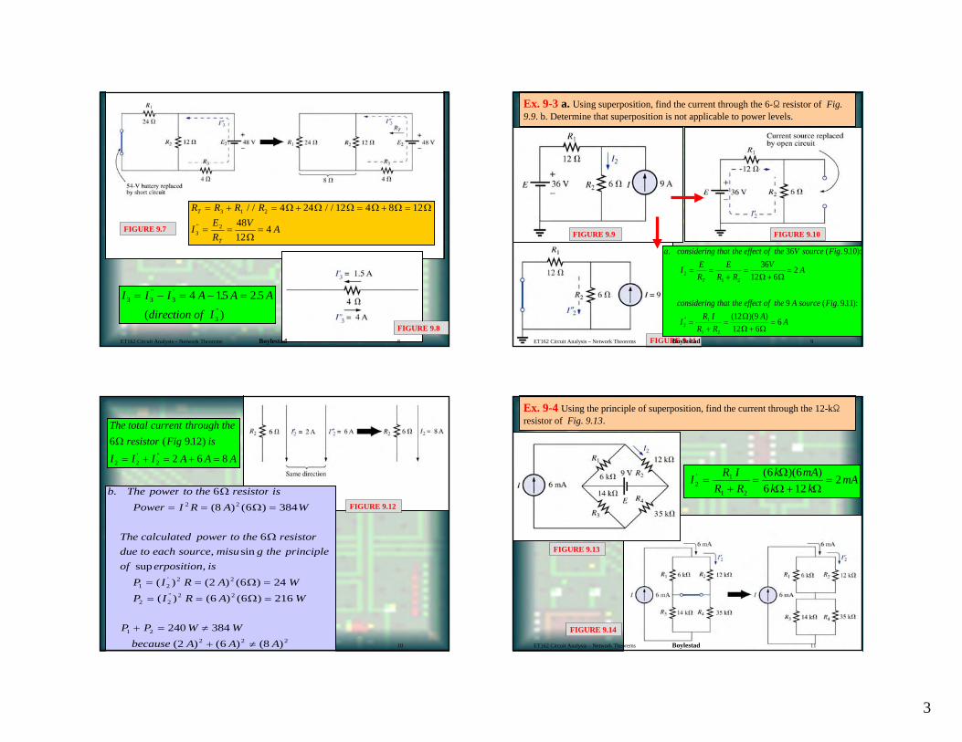
3
R R R R
I ER
V A
T
T
= + = + = + =
= = =
3 1 2
32
4 24 12 4 8 124812
4
/ / / /
''
Ω Ω Ω Ω Ω Ω
Ω
I I I A A Adirection of I
3 3 3
3
4 15 2 5= − = − ='' '
''
. .( )
FIGURE 9.7
FIGURE 9.8ET162 Circuit Analysis – Network Theorems Boylestad 8
Ex. 9-3 a. Using superposition, find the current through the 6-Ω resistor of Fig. 9.9. b. Determine that superposition is not applicable to power levels.
FIGURE 9.9
FIGURE 9.11
FIGURE 9.10
a considering that the effect of the V source Fig
I ER
ER R
VA
considering that the effect of the A source Fig
IR I
R RA
A
T
. ( . . ):
( . . ):( )( )
'
''
36 91036
12 62
9 91112 912 6
6
21 2
21
1 2
= =+
=+
=
=+
=+
=
Ω Ω
ΩΩ Ω
ET162 Circuit Analysis – Network Theorems Boylestad 9
The total current through theresistor Fig is
I I I A A A6 912
2 6 82 2 2
Ω ( . )' ''= + = + =
FIGURE 9.12
ET162 Circuit Analysis – Network Theorems 10
b The power to the resistor isPower I R A W
The calculated power to the resistordue to each source misu g the principleof erposition is
P I R A WP I R A W
P P W Wbecause A A A
.(8 ) ( )
, sinsup ,
( ) ( ) ( )( ) ( ) ( )
( ) ( ) (8 )
'
''
66 384
6
2 6 246 6 216
240 3842 6
2 2
1 22 2
2 22 2
1 22 2 2
Ω
Ω
Ω
Ω
Ω
= = =
= = =
= = =
+ = ≠
+ ≠
FIGURE 9.13
Ex. 9-4 Using the principle of superposition, find the current through the 12-kΩresistor of Fig. 9.13.
FIGURE 9.14
I R IR R
k mAk k
mA21
1 2
6 66 12
2' ( )( )=
+=
+=
ΩΩ Ω
ET162 Circuit Analysis – Network Theorems Boylestad 11
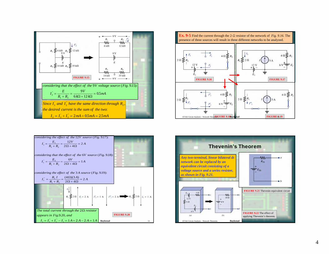
4
considering that the effect of the V voltage source Fig
I ER R
Vk k
mA
9 9159
6 12052
1 2
( . . ):
.'' =+
=+
=Ω Ω
12
FIGURE 9.15
Since I and I have the same direction through Rthe desired current is the sum of the two
I I I mA mA mA
2 2 2
2 2 2 2 05 2 5
' ''
' ''
,:
. .= + = + =
FIGURE 9.16
Ex. 9-5 Find the current through the 2-Ω resistor of the network of Fig. 9.16. The presence of three sources will result in three different networks to be analyzed.
FIGURE 9.18 FIGURE 9.19
FIGURE 9.17
ET162 Circuit Analysis – Network Theorems Boylestad 13
ET162 Circuit Analysis – Methods of Analysis Boylestad 14
FIGURE 9.20
considering the effect of the V source Fig
IE
R RV
A
considering that the effect of the V source Fig
IE
R RV
A
considering the effect of the A source Fig
I R IR R
A A
12 91712
2 42
6 9186
2 41
3 9194 32 4
2
11
1 2
12
1 2
12
1 2
( . . ):
( . . ):
( . . ):( )( )
'
''
'''
=+
=+
=
=+
=+
=
=+
=+
=
Ω Ω
Ω Ω
ΩΩ Ω
The total current through the resistorappears in Fig and
I I I I A A A A
29 20
1 2 2 11 1 1 1
Ω. . ,
'' ''' '= + − = + − =
Thevenin’s Theorem
FIGURE 9.21 Thevenin equivalent circuit
Any two-terminal, linear bilateral dc network can be replaced by an equivalent circuit consisting of a voltage source and a series resistor, as shown in Fig. 9.21.
FIGURE 9.22 The effect of applying Thevenin’s theorem.
ET162 Circuit Analysis – Network Theorems Boylestad 15
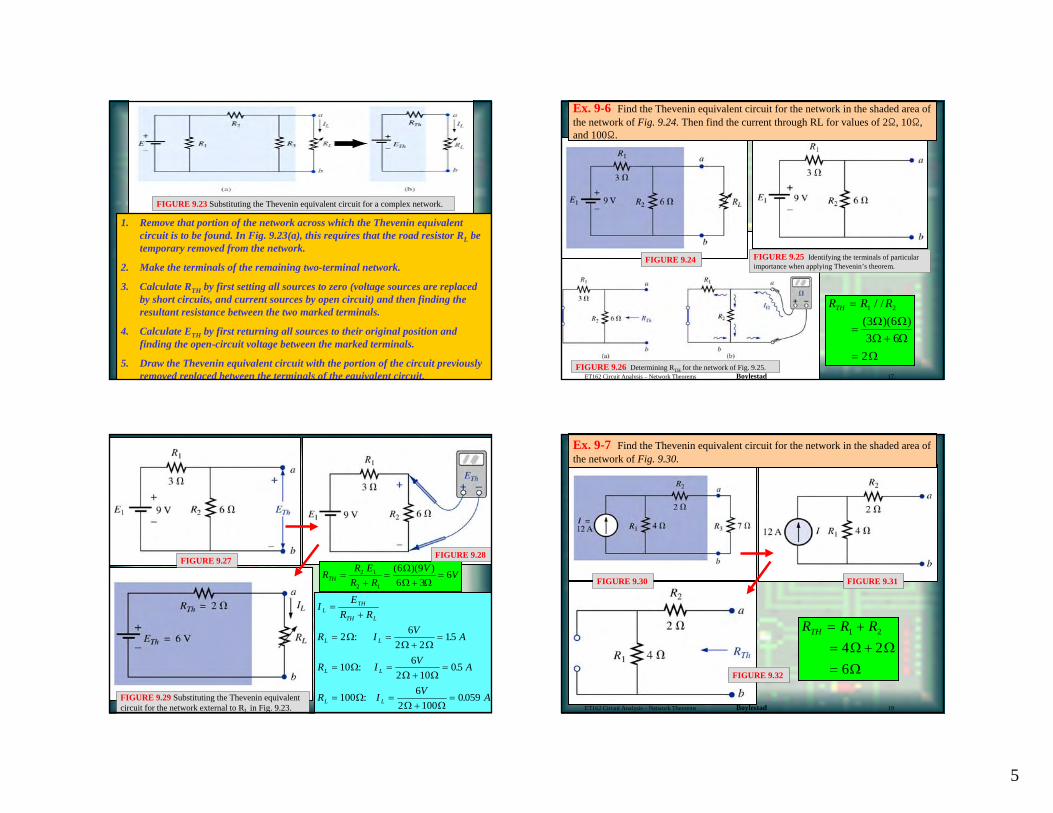
5
ET162 Circuit Analysis – Methods of Analysis Boylestad 16
FIGURE 9.23 Substituting the Thevenin equivalent circuit for a complex network.
1. Remove that portion of the network across which the Thevenin equivalent circuit is to be found. In Fig. 9.23(a), this requires that the road resistor RL be temporary removed from the network.
2. Make the terminals of the remaining two-terminal network.
3. Calculate RTH by first setting all sources to zero (voltage sources are replaced by short circuits, and current sources by open circuit) and then finding the resultant resistance between the two marked terminals.
4. Calculate ETH by first returning all sources to their original position and finding the open-circuit voltage between the marked terminals.
5. Draw the Thevenin equivalent circuit with the portion of the circuit previously removed replaced between the terminals of the equivalent circuit.
Ex. 9-6 Find the Thevenin equivalent circuit for the network in the shaded area of the network of Fig. 9.24. Then find the current through RL for values of 2Ω, 10Ω, and 100Ω.
FIGURE 9.24 FIGURE 9.25 Identifying the terminals of particular importance when applying Thevenin’s theorem.
R R RTH =
=+
=
1 2
3 63 6
2
/ /( )( )Ω ΩΩ ΩΩ
FIGURE 9.26 Determining RTH for the network of Fig. 9.25.ET162 Circuit Analysis – Network Theorems Boylestad 17
18
IE
R R
R IV
A
R IV
A
R IV
A
LTH
TH L
L L
L L
L L
=+
= =+
=
= =+
=
= =+
=
26
2 215
106
2 1005
1006
2 1000 059
ΩΩ Ω
ΩΩ Ω
ΩΩ Ω
: .
: .
: .
FIGURE 9.27
R R ER R
V VTH =+
=+
=2 1
2 1
6 96 3
6( )( )ΩΩ Ω
FIGURE 9.29 Substituting the Thevenin equivalent circuit for the network external to RL in Fig. 9.23.
FIGURE 9.28
Ex. 9-7 Find the Thevenin equivalent circuit for the network in the shaded area of the network of Fig. 9.30.
R R RTH = += +=
1 2
4 26Ω ΩΩ
FIGURE 9.30 FIGURE 9.31
FIGURE 9.32
ET162 Circuit Analysis – Network Theorems Boylestad 19
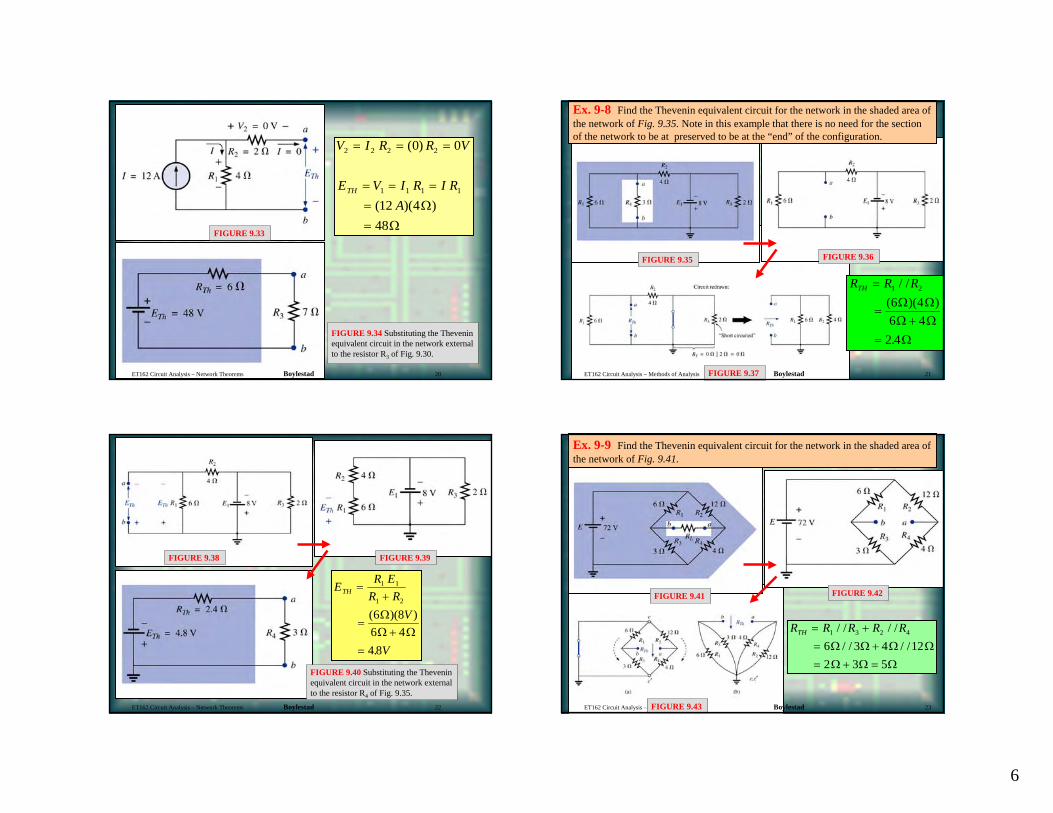
6
FIGURE 9.33
FIGURE 9.34 Substituting the Theveninequivalent circuit in the network external to the resistor R3 of Fig. 9.30.
V I R R V
E V I R I RA
TH
2 2 2 2
1 1 1 1
0 0
12 448
= = =
= = ===
( )
( )( )ΩΩ
ET162 Circuit Analysis – Network Theorems Boylestad 20 ET162 Circuit Analysis – Methods of Analysis Boylestad 21
FIGURE 9.35
Ex. 9-8 Find the Thevenin equivalent circuit for the network in the shaded area of the network of Fig. 9.35. Note in this example that there is no need for the section of the network to be at preserved to be at the “end” of the configuration.
R R RTH =
=+
=
1 2
6 46 4
2 4
/ /( )( )
.
Ω ΩΩ ΩΩ
FIGURE 9.37
FIGURE 9.36
FIGURE 9.38
E R ER R
V
V
TH =+
=+
=
1 1
1 2
66 44 8
( )(8 )
.
ΩΩ Ω
FIGURE 9.40 Substituting the Theveninequivalent circuit in the network external to the resistor R4 of Fig. 9.35.
FIGURE 9.39
ET162 Circuit Analysis – Network Theorems Boylestad 22 ET162 Circuit Analysis – Methods of Analysis Boylestad 23
Ex. 9-9 Find the Thevenin equivalent circuit for the network in the shaded area of the network of Fig. 9.41.
R R R R RTH = += += + =
1 3 2 4
6 3 4 122 3 5
/ / / // / / /Ω Ω Ω Ω
Ω Ω Ω
FIGURE 9.43
FIGURE 9.42FIGURE 9.41
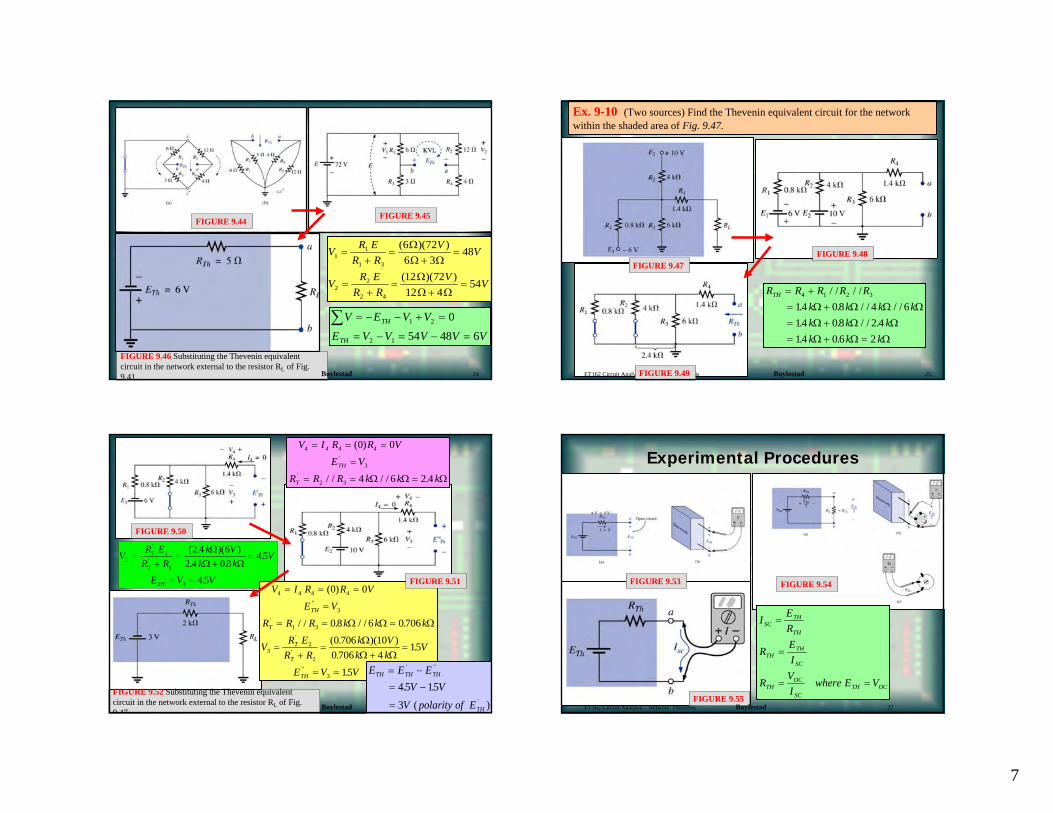
7
V R ER R
V V
VR E
R RV
V
11
1 3
22
2 4
6 726 3
48
12 7212 4
54
=+
=+
=
=+
=+
=
( )( )
( )( )
ΩΩ ΩΩΩ Ω
V E V V
E V V V V VTH
TH
∑ = − − + =
= − = − =1 2
2 1
0
54 48 6FIGURE 9.46 Substituting the Thevenin equivalent circuit in the network external to the resistor RL of Fig. 9.41.
FIGURE 9.45FIGURE 9.44
Boylestad 24 ET162 Circuit Analysis – Methods of Analysis Boylestad 25
FIGURE 9.47
Ex. 9-10 (Two sources) Find the Thevenin equivalent circuit for the network within the shaded area of Fig. 9.47.
R R R R Rk k k kk k kk k k
TH = += += += + =
4 1 2 3
14 08 4 614 08 2 414 0 6 2
/ / / /. . / / / /. . / / .. .
Ω Ω Ω ΩΩ Ω ΩΩ Ω Ω
FIGURE 9.48
FIGURE 9.49
ET162 Circuit Analysis – Methods of Analysis Boylestad 26
FIGURE 9.52 Substituting the Thevenin equivalent circuit in the network external to the resistor RL of Fig. 9 47
V I R R VE V
R R R k k kTH
T
4 4 4 4
3
2 3
0 0
4 6 2 4
= = =
=
= = =
( )
/ / / / .
'
' Ω Ω Ω
VR E
R Rk V
k kV
E V V
T
T
TH
31
1
3
2 4 62 4 08
4 5
4 5
=+
=+
=
= =
'
'
'
( . )( ). .
.
.
ΩΩ Ω
V I R R VE V
R R R k k k
V R ER R
k Vk k
V
E V V
TH
T
T
T
TH
4 4 4 4
3
1 3
32
2
3
0 0
08 6 0 7060 706 100 706 4
15
15
= = =
=
= = =
=+
=+
=
= =
( )
/ / . / / .( . )( )
..
.
''
'
'
'
''
Ω Ω Ω
ΩΩ Ω
E E EV V
V polarity of E
TH TH TH
TH
= −= −
=
' ''
'
. .( )
4 5 153
FIGURE 9.51
FIGURE 9.50
Experimental Procedures
IER
R EI
RVI
where E V
SCTH
TH
THTH
SC
THOC
SCTH OC
=
=
= =
FIGURE 9.53 FIGURE 9.54
FIGURE 9.55ET162 Circuit Analysis – Network Theorems Boylestad 27
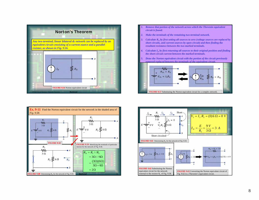
8
Norton’s Theorem
Any two-terminal, linear bilateral dc network can be replaced by an equivalent circuit consisting of a current source and a parallelresistor, as shown in Fig. 9.56.
FIGURE 9.56 Norton equivalent circuit
ET162 Circuit Analysis – Network Theorems Boylestad 28
1. Remove that portion of the network across which the Thevenin equivalent circuit is found.
2. Make the terminals of the remaining two-terminal network.
3. Calculate RN by first setting all sources to zero (voltage sources are replaced by short circuits, and current sources by open circuit) and then finding the resultant resistance between the two marked terminals.
4. Calculate IN by first returning all sources to their original position and finding the short-circuit current between the marked terminals.
5. Draw the Norton equivalent circuit with the portion of the circuit previously removed replaced between the terminals of the equivalent circuit.
FIGURE 9.57 Substituting the Norton equivalent circuit for a complex network. 29
Ex. 9-11 Find the Norton equivalent circuit for the network in the shaded area of Fig. 9.58.
FIGURE 9.59 Identifying the terminals of particular interest for the network of Fig. 9.58.
FIGURE 9.58
FIGURE 9.60 Determining RN for the network of Fig. 9.59.
R R RN ==
=+
=
1 2
3 63 63 6
2
/ // /
( )( )Ω ΩΩ ΩΩ ΩΩ
Boylestad 30
V I R V
I ER
V AN
2 2 2
1
0 6 0
93
3
= = =
= = =
( ) Ω
Ω
FIGURE 9.61 Determining RN for the network of Fig. 9.59.
FIGURE 9.62 Substituting the Norton equivalent circuit for the network external to the resistor RL of Fig. 9.58.
FIGURE 9.63 Converting the Norton equivalent circuit of Fig. 9.62 to a Thevenin’s equivalent circuit.
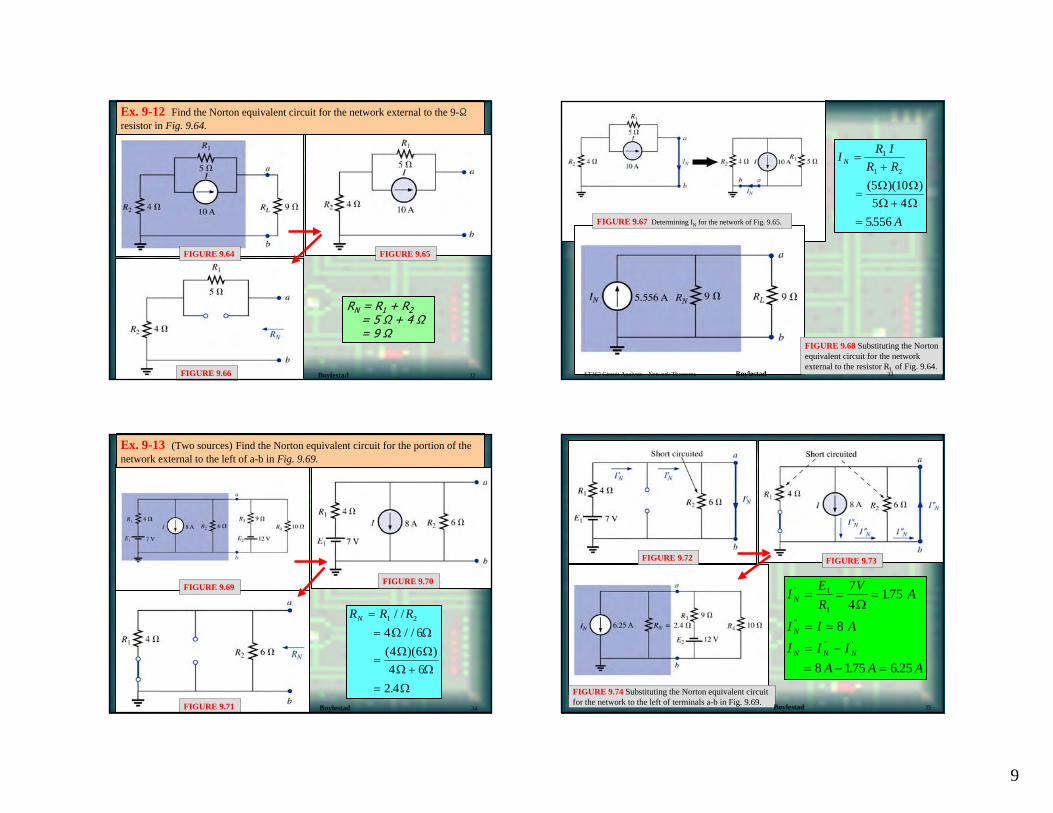
9
Ex. 9-12 Find the Norton equivalent circuit for the network external to the 9-Ωresistor in Fig. 9.64.
RN = R1 + R2= 5 Ω + 4 Ω= 9 Ω
FIGURE 9.64 FIGURE 9.65
FIGURE 9.66 Boylestad 32
I R IR R
A
N =+
=+
=
1
1 2
105 4
5556
(5 )( )
.
Ω ΩΩ Ω
FIGURE 9.67 Determining IN for the network of Fig. 9.65.
FIGURE 9.68 Substituting the Norton equivalent circuit for the network external to the resistor RL of Fig. 9.64.
ET162 Circuit Analysis – Network Theorems Boylestad 33
Ex. 9-13 (Two sources) Find the Norton equivalent circuit for the portion of the network external to the left of a-b in Fig. 9.69.
R R RN ==
=+
=
1 2
4 64 64 6
2 4
/ // /
( )( )
.
Ω ΩΩ ΩΩ ΩΩ
FIGURE 9.69FIGURE 9.70
FIGURE 9.71 Boylestad 34
I ER
V A
I I AI I I
A A A
N
N
N N N
'
''
'' '
.
. .
= = =
= =
= −= − =
1
1
74
175
8
8 175 6 25
Ω
FIGURE 9.74 Substituting the Norton equivalent circuit for the network to the left of terminals a-b in Fig. 9.69.
FIGURE 9.72 FIGURE 9.73
Boylestad 35
10
Maximum Power Transfer Theorem
A load will receive maximum power from a linear bilateral dc network when its total resistive value is exactly equal to the Thevenin resistance of the network as “seen” by the load.
FIGURE 9.74 Defining the conditions for maximum power to a load using the Thevenin equivalent circuit.
FIGURE 9.75 Defining the conditions for maximum power to a load using the Norton equivalent circuit.
RL = RTH RL = RN
ET162 Circuit Analysis – Network Theorems Boylestad 36
Homework 9: 2, 4, 6, 13, 14
HW 9-6 Using superposition, find the voltage V2 for the network in Fig. 9.124.
Figure 9.124 Problem 6.
VkkVkV
02.13128.6
)36(8.6'1
=Ω+Ω
Ω=
mAkk
mAkI
75.58.612
)9(122
=Ω+Ω
Ω=
VVVVVV
VkmARIV
12.5210.3902.13
10.39)8.6)(75.5(''
2'
12
22''
2
=+=+=
=Ω==
ET162 Circuit Analysis – Network Theorems Boylestad 37
1
Capacitors
EET1122/ET162 Circuit Analysis
Electrical and Telecommunications Engineering Technology Department
Professor JangPrepared by textbook based on “Introduction to Circuit Analysis”
by Robert Boylestad, Prentice Hall, 10th edition.
OUTLINESOUTLINES
Introduction to Capacitors
The Electric Field
Capacitance
Capacitors in Series and Parallel
Transients in Capacitive Networks: Charging Phase
ET162 Circuit Analysis – Capacitors Boylestad 2
Key Words: Capacitor, Electric Field, Capacitance, Transient
Introduction to Capacitors
Thus far, the only passive device appearing in the class has been the resistor. We will now consider two additional passive devices called the capacitor and the inductor, which are quite different from the resistor in purpose, operation, and construction.
Unlike the resistor, both elements display their total characteristics only when a change in voltage or current is made in the circuit in which they exist. In addition, if we consider the ideal situation, they do not dissipate energy as does the resistor but store it in a form that can be returned to the circuit whenever required by the circuit design.
ET162 Circuit Analysis – Capacitors Boylestad 3 ET162 Circuit Analysis – Capacitors Boylestad 4
The Electric Field
DA
flux unit area=ψ ( / )
The electric field is represented by electric flux lines, which are drawn to indicate the strength of the electric field at any point around any charged body; that is, the denser the lines of flux, the stronger the electric field. In Fig. 10.1, the electric field strength is stronger at point a than at position b because the flux lines are denser at a than b.
The flux per unit area (flux density) is represented by the capital letter D and is determined by
FIGURE 10.1 Flux distribution from an isolated positive charge.
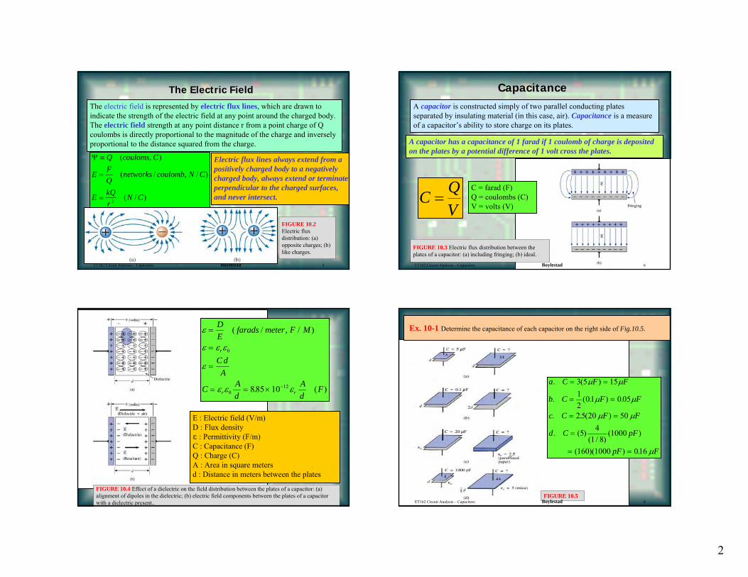
2
ET162 Circuit Analysis – Capacitors Boylestad 5
The Electric FieldThe Electric Field
The electric field is represented by electric flux lines, which are drawn to indicate the strength of the electric field at any point around the charged body. The electric field strength at any point distance r from a point charge of Q coulombs is directly proportional to the magnitude of the charge and inversely proportional to the distance squared from the charge.
Electric flux lines always extend from a positively charged body to a negatively charged body, always extend or terminate perpendicular to the charged surfaces, and never intersect.)/(
)/,/(
),(
2 CNrkQE
CNcoulombnetworksQFE
CcoulomsQ
=
=
≡Ψ
FIGURE 10.2 Electric flux distribution: (a) opposite charges; (b) like charges.
FIGURE 10.3 Electric flux distribution between the plates of a capacitor: (a) including fringing; (b) ideal.
VQC =
CapacitanceCapacitanceA capacitor is constructed simply of two parallel conducting plates separated by insulating material (in this case, air). Capacitance is a measure of a capacitor’s ability to store charge on its plates.
A capacitor has a capacitance of 1 farad if 1 coulomb of charge is deposited on the plates by a potential difference of 1 volt cross the plates.
C = farad (F)Q = coulombs (C)V = volts (V)
ET162 Circuit Analysis – Capacitors Boylestad 6
ET162 Circuit Analysis – Capacitors Boylestad 7
FIGURE 10.4 Effect of a dielectric on the field distribution between the plates of a capacitor: (a) alignment of dipoles in the dielectric; (b) electric field components between the plates of a capacitor with a dielectric present..
ε
ε ε ε
ε
ε ε ε
=
=
=
= = × −
DE
farads meter F M
C dA
C Ad
Ad
F
r
r r
( / , / )
. ( )
0
012885 10
E : Electric field (V/m)D : Flux densityε : Permittivity (F/m)C : Capacitance (F)Q : Charge (C)A : Area in square meters d : Distance in meters between the plates
Ex. 10-1 Determine the capacitance of each capacitor on the right side of Fig.10.5.
FIGURE 10.5
a C F F
b C F F
c C F F
d C pF
pF F
. (5 )
. ( . ) .
. . ( )
. (5)( / )
( )
( )( ) .
= =
= =
= =
=
= =
3 1512
01 0 05
2 5 20 504
1 81000
160 1000 016
µ µ
µ µ
µ µ
µ
ET162 Circuit Analysis – Capacitors Boylestad 8
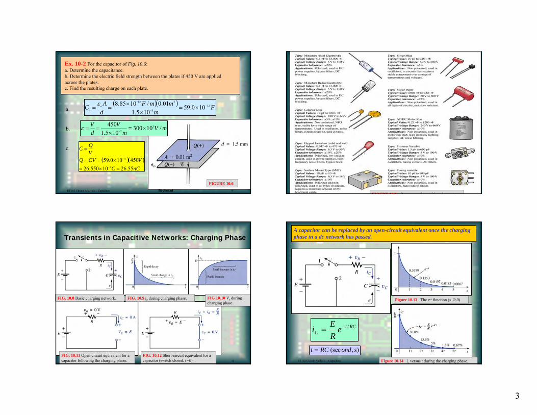
3
Ex. 10-2 For the capacitor of Fig. 10.6:a. Determine the capacitance.b. Determine the electric field strength between the plates if 450 V are applied across the plates.c. Find the resulting charge on each plate.
( )( ) Fm
mmFdAC o
o12
3
212
100.59105.1
01.0/1085.8 −
−
−
×=×
×==
ε
mVm
VdV /10300
105.1450 3
3×≅
×==
−ε
( )( )nCC
VCVQVQC
55.2610550.26450100.59
9
12
=×=
×==
=
−
−
a.
b.
c.
FIGURE 10.6ET162 Circuit Analysis – Capacitors Boylestad 9
FIGURE 10 7 Summary of capacitive elements
ET162 Circuit Analysis – Capacitors Boylestad 11
Transients in Capacitive Networks: Charging Phase
FIG. 10.8 Basic charging network. FIG. 10.9 ic during charging phase. FIG 10.10 Vc during charging phase.
FIG. 10.11 Open-circuit equivalent for a capacitor following the charging phase.
FIG. 10.12 Short-circuit equivalent for a capacitor (switch closed, t=0). ET162 Circuit Analysis – Capacitors Boylestad 22
A capacitor can be replaced by an open-circuit equivalent once the charging phase in a dc network has passed.
i ER
eCt RC= − /
t RC ond s= (sec , )
Figure 10.13 The e-x function (x ≥ 0).
Figure 10.14 ic versus t during the charging phase.
4
v E eCt RC= − −( )/1
v EeRt RC= − /
Figure 10.15 vc versus t during the charging phase. Figure 10.16 Effect of C on the charging phase.
Figure 10.17 vR versus t during the charging phase.ET162 Circuit Analysis – Capacitors Boylestad 13 ET162 Circuit Analysis – Capacitors Boylestad 14
Ex. 10-3 a. Find the mathematical expressions for the transient behavior of vC, iC, and vRfor the circuit of Fig. 10.18 when the switch is moved to position 1. Plot the curves of vC, iC, and vR.b. How much time must pass before it can be assumed, for all practical purposes, that iC ≈0 A and vC≈ E volt?
a RC Fs ms
v E e e
i ER
eV
ke
e
v Ee eb ms ms
Ct t
Ct t
t
Rt t
. (8 )( )
( ) ( )
(5 )
. ( )
/ /( )
/ /( )
/( )
/ /( )
τ
τ
τ
τ
τ
= = × ×
= × =
= − = −
= =
= ×
= == =
−
−
− − ×
− − ×
− − ×
− − ×
−
−
−
−
10 4 1032 10 32
1 40 1808
10
405 5 32 160
3 6
3
32 10
32 10
3 32 10
32 10
3
3
3
3
Ω
Ω
FIGURE 10.18
FIGURE 10.19
Transients in Capacitive Networks: Discharging Phase v Ee disch ing
i ER
e disch ing
v Ee disch ing
Ct RC
Ct RC
Ct RC
=
= −
= −
−
−
−
/
/
/
: arg
arg
arg
Figure 10.20 Demonstrating the discharge behavior of a capacitive network.
Figure 10.21 The charging and discharging cycles for the network of fig. 10.19.
ET162 Circuit Analysis – Capacitors 15
τ =
= =
= − = − ×
= − = −
− − ×
− − − ×
− − ×
−
−
−
32
40
10
40
32 10
3 32 10
32 10
3
3
3
ms
v Ee e
i ER
e e
v Ee e
Ct RC t
Ct RC t
Ct RC t
/ /
/ /
/ /
( )
(5 )
Ex. 10-4 After vC in Example 10.3 has reached its final value of 40 V, the switch is shown into position 2, as shown in Fig. 10.21. Find the mathematical expressions for the transient behavior of vC, iC, and vR after the closing of the switch. Plot the curves for vC, iC, and vR using the defined directions and polarities of Fig. 10.18. Assume that t = 0 when the switch is moved to position 2.
FIGURE 10.23
FIGURE 10.21
5
ET162 Circuit Analysis – Capacitors Boylestad 17
Capacitors in Series and Parallel
Q Q Q Q
C C C C
C C CC C
T
T
T
= = =
= = =
=+
1 2 3
1 2 3
1 2
1 2
1 1 1 1
Figure 10.24 Series capacitors.
Q Q Q QC C C C
T
T
= + += + +
1 2 3
1 2 3
Figure 10.25 Parallel capacitors. ET162 Circuit Analysis – Capacitors Boylestad 18
Ex. 10-5 For the circuit of Fig. 10.26:a. Find the total capacitance.b. Determine the charge on each plate.c. Find the voltage across each capacitor.
aC C C C
F F F
C F
T
T
.
.
.
1 1 1 1
1200 10
150 10
110 10
0125 101
0125 108
1 2 3
6 6 6
6
6
= + +
=×
+×
+×
= ×
=×
=
− − −
µ
b Q Q Q QC E F V
C
T
T
.(8 )( )
= = =
= = ×=
−
1 2 3610 60
480 µ
c VQC
CF
V
VQC
CF
V
VQC
CF
V
and E V V V V
. .
.
.
11
1
6
6
22
2
6
6
33
3
6
6
1 2 3
480 10200 10
2 4
480 1050 10
9 6
480 10100 10
48 0
60
= =××
=
= =××
=
= =××
=
= + + =
−
−
−
−
−
−
Figure 10.26
Ex. 10-6 For the circuit of Fig. 10.27:a. Find the total capacitance.b. Determine the charge on each plate.c. Find the total charges.
a C C C CF F F
Fb Q C E F V mC
Q C E F V mCQ C E F V mC
c Q Q Q Q mC
T
T
.
. (800 )( ) .( )( ) .( )( ) .
. .
= + += + +=
= = × =
= = × =
= = × == + + =
−
−
−
1 2 3
1 16
2 26
3 16
1 2 3
800 60 12002060
10 48 38 460 10 48 2 881200 10 48 57 6
9888
µ µ µµ
Figure 10.27
ET162 Circuit Analysis – Capacitors Boylestad 19
Ex. 10-7 Find the voltage across and charge on each capacitor for the network of Fig. 10.28.
C C C F F F
CC C
C CF FF F
F
Q C E F V C
T
TT
T
T T
'
'
'
( )( )
( )( )
= + = + =
=+
=+
=
= = × =−
2 3
1
16
4 2 63 63 6
2
2 10 120 240
µ µ µ
µ µµ µ
µ
µ
Q Q QQ C
VQC
CF
V
Q C
T T
T
= ==
= =×
×=
=
−
−
1
1
11
1
6
6
240240 103 10
80
240
'
'
µ
µ
VQC
CF
V
Q C V F V CQ C V F V C
TT
T
T
T
''
'
'
'
( )( )( )( )
= =××
=
= = × =
= = × =
−
−
−
−
240 106 10
40
4 10 40 1602 10 40 80
6
6
2 26
3 36
µ
µ
Figure 10.28
Figure 10.29
ET162 Circuit Analysis – Capacitors Boylestad 20
6
ET162 Circuit Analysis – Capacitors Boylestad 21
Ex. 10-8 Find the voltage across and charge on capacitors C1 of Fig. 10.30 after it has charged up to its final value.
VV
V
Q C VF V
C
C
C
=+
=
=
= ×=
−
(8 )( )
( )( )
ΩΩ Ω
244 8
16
20 10 16320
1 16
µ
Figure 10.30
Figure 10.31
Ex. 10-9 Find the voltage across and charge on each capacitor for the network of Fig. 10.32. after each has charged up to its final value.
V V V
VV
V
Q C V F V C
Q C V F V C
C
C
C
C
2
1
1
2
7 727 2
76
2 727 2
16
2 10 16 32
3 10 1681 1
6
1 26
=+
=
=+
=
= = × =
= = × =
−
−
( )( )
( )( )
( )( )
( )(56 )
ΩΩ ΩΩΩ Ω
µ
µ
Figure 10.32
ET162 Circuit Analysis – Capacitors Boylestad 22
HW 10-54 Find the voltage across and the charge on each capacitor for the circuit in Fig. 10.115.
Figure 10.115 Problem 54.
Homework 10: 3, 4, 14, 51,52, 54, 57
HW 10-22 Repeat Problem 21 for R = 1 MΩ, and compare the results.
Figure 10.87 Problem 22.
Homework 10: 22, 24, 27, 28
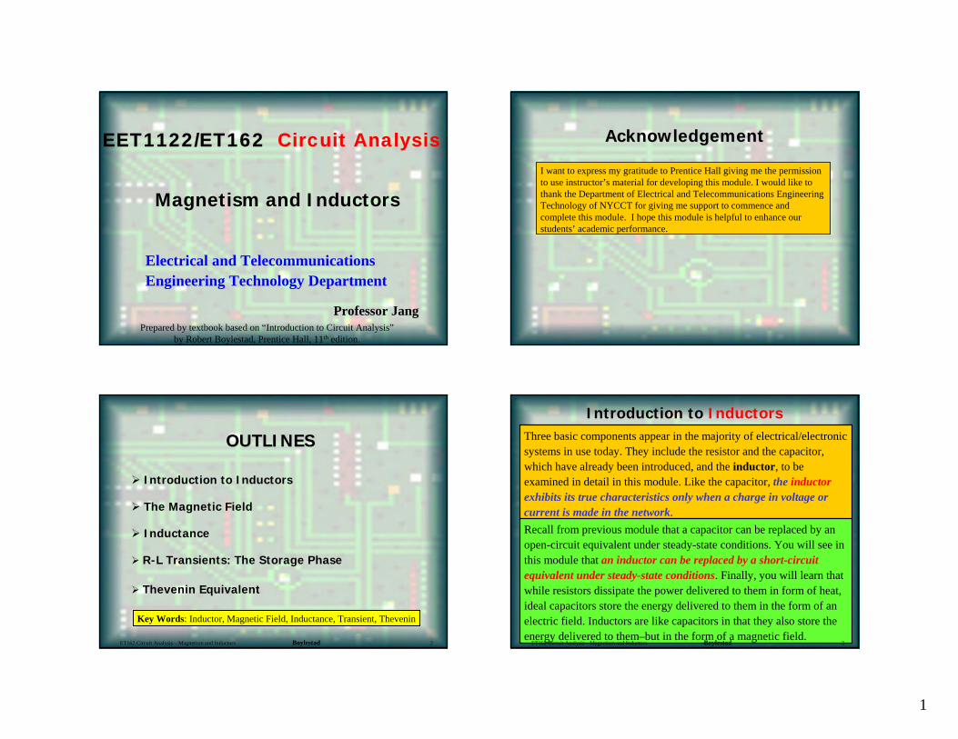
1
Magnetism and Inductors
EET1122/ET162 Circuit Analysis
Electrical and Telecommunications Engineering Technology Department
Professor JangPrepared by textbook based on “Introduction to Circuit Analysis”
by Robert Boylestad, Prentice Hall, 11th edition.
AcknowledgementAcknowledgement
I want to express my gratitude to Prentice Hall giving me the permission to use instructor’s material for developing this module. I would like to thank the Department of Electrical and Telecommunications Engineering Technology of NYCCT for giving me support to commence and complete this module. I hope this module is helpful to enhance our students’ academic performance.
OUTLINESOUTLINES
Introduction to Inductors
The Magnetic Field
Inductance
Thevenin Equivalent
R-L Transients: The Storage Phase
Key Words: Inductor, Magnetic Field, Inductance, Transient, Thevenin
ET162 Circuit Analysis – Magnetism and Inductors Boylestad 2
Introduction to InductorsThree basic components appear in the majority of electrical/electronic systems in use today. They include the resistor and the capacitor, which have already been introduced, and the inductor, to be examined in detail in this module. Like the capacitor, the inductorexhibits its true characteristics only when a charge in voltage or current is made in the network.Recall from previous module that a capacitor can be replaced by an open-circuit equivalent under steady-state conditions. You will see in this module that an inductor can be replaced by a short-circuit equivalent under steady-state conditions. Finally, you will learn that while resistors dissipate the power delivered to them in form of heat, ideal capacitors store the energy delivered to them in the form of an electric field. Inductors are like capacitors in that they also store the energy delivered to them–but in the form of a magnetic field.
ET162 Circuit Analysis – Magnetism and Inductors Boylestad 3
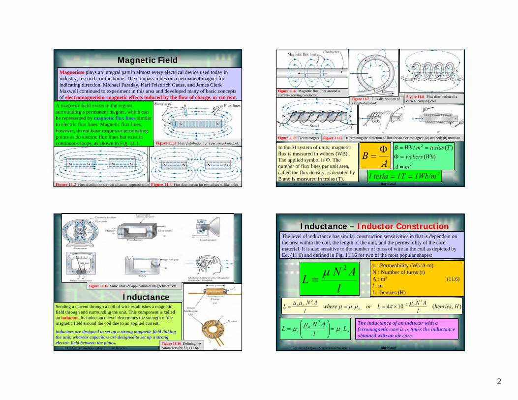
2
ET162 Circuit Analysis – Capacitors Boylestad 4
Magnetic FieldMagnetism plays an integral part in almost every electrical device used today in industry, research, or the home. The compass relies on a permanent magnet for indicating direction. Michael Faraday, Karl Friedrich Gauss, and James Clerk Maxwell continued to experiment in this area and developed many of basic concepts of electromagnetism–magnetic effects induced by the flow of charge, or current.
A magnetic field exists in the region surrounding a permanent magnet, which can be represented by magnetic flux lines similar to electric flux lines. Magnetic flux lines, however, do not have origins or terminating points as do electric flux lines but exist in continuous loops, as shown in Fig. 11.1. Figure 11.1 Flux distribution for a permanent magnet.
Figure 11.2 Flux distribution for two adjacent, opposite poles. Figure 11.3 Flux distribution for two adjacent, like poles.
In the SI system of units, magnetic flux is measured in webers (WB). The applied symbol is Φ. The number of flux lines per unit area, called the flux density, is denoted by B and is measured in teslas (T).
Figure 11.6 Magnetic flux lines around a current-carrying conductor.
Figure 11.7 Flux distribution of a single-turn coil.
Figure 11.8 Flux distribution of a current carrying coil.
Figure 11.9 Electromagnet. Figure 11.10 Determining the direction of flux for an electromagnet: (a) method; (b) notation.
AB Φ=
2
2
)()(/
mAWbwebers
TteslasmWbB
=
=Φ==
2Wb/m1T1tesla1 ==ET162 Circuit Analysis – Magnetism and Inductors Boylestad 5
ET162 Circuit Analysis – Magnetism and Inductors Boylestad 21
InductanceInductanceSending a current through a coil of wire establishes a magnetic field through and surrounding the unit. This component is calledan inductor. Its inductance level determines the strength of the magnetic field around the coil due to an applied current.
inductors are designed to set up a strong magnetic field linkingthe unit, whereas capacitors are designed to set up a strong electric field between the plates.
Figure 11.15 Some areas of application of magnetic effects.
Figure 11.16 Defining the parameters for Eq. (11.6).
μ : Permeability (Wb/A∙m)N : Number of turns (t)A : m2 (11.6)l : mL : henries (H)
Inductance Inductance –– Inductor ConstructionInductor Construction
lANL
2µ=
),(1042
72
Hhenriesl
ANLorwherel
ANL r
oror µ
πµµµµµ −×===
The level of inductance has similar construction sensitivities in that is dependent on the area within the coil, the length of the unit, and the permeability of the core material. It is also sensitive to the number of turns of wire in the coil as depicted by Eq. (11.6) and defined in Fig. 11.16 for two of the most popular shapes:
oro
r Ll
ANL µ
µµ =⎟⎟
⎠
⎞⎜⎜⎝
⎛=
2 The inductance of an inductor with a ferromagnetic core is μr times the inductance obtained with an air core.
ET162 Circuit Analysis – Magnetism and Inductors Boylestad 7
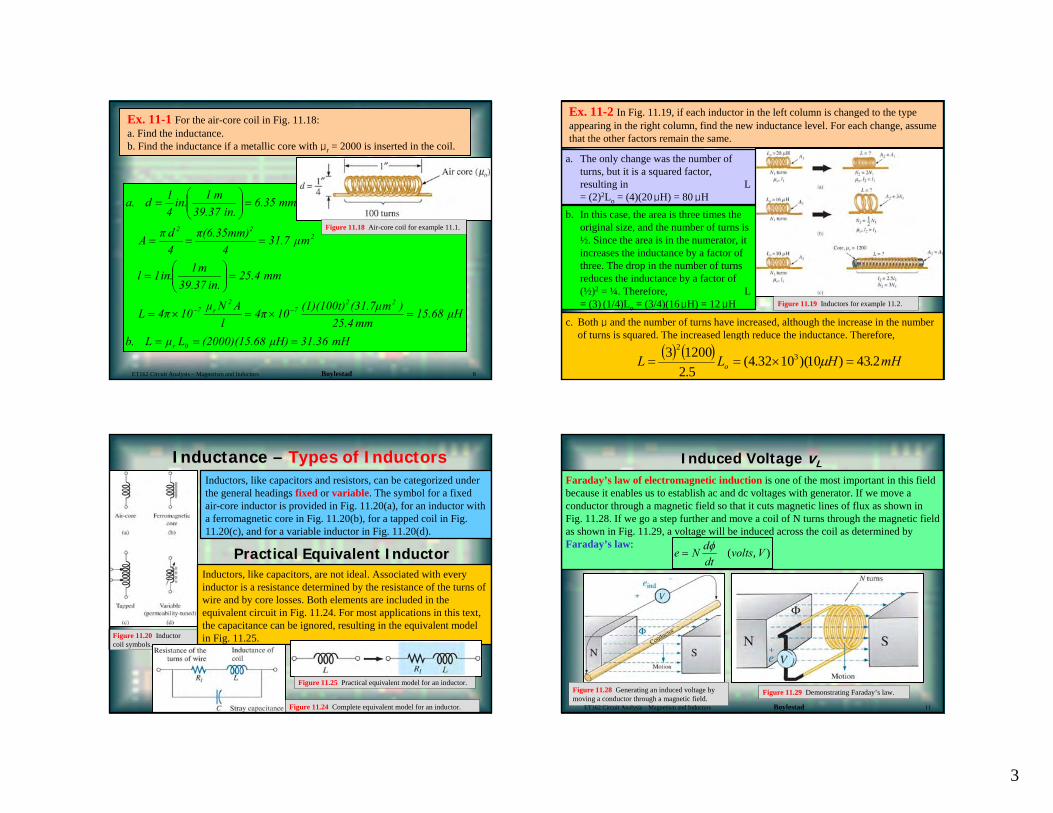
3
Ex. 11-1 For the air-core coil in Fig. 11.18:a. Find the inductance.b. Find the inductance if a metallic core with μr = 2000 is inserted in the coil.
mH31.36µH)68(2000)(15.LµLb.
µH15.68mm25.4
)m(31.7µ(1)(100t)104πl
ANµ104πL
mm25.4in.39.37
m1in.1l
mµ31.74
π(6.35mm)4dπA
mm6.35in.39.37
m1in.41da.
0r
227
2r7
222
===
=×=×=
=⎟⎟⎠
⎞⎜⎜⎝
⎛=
===
=⎟⎟⎠
⎞⎜⎜⎝
⎛=
−−
Figure 11.18 Air-core coil for example 11.1.
ET162 Circuit Analysis – Magnetism and Inductors Boylestad 8
Ex. 11-2 In Fig. 11.19, if each inductor in the left column is changed to the type appearing in the right column, find the new inductance level. For each change, assume that the other factors remain the same.
ET162 Circuit Analysis – Capacitors Boylestad 9
a. The only change was the number of turns, but it is a squared factor, resulting in L = (2)2Lo = (4)(20μH) = 80 μH
b. In this case, the area is three times the original size, and the number of turns is ½. Since the area is in the numerator, it increases the inductance by a factor of three. The drop in the number of turns reduces the inductance by a factor of (½)2 = ¼. Therefore, L = (3) (1/4)Lo = (3/4)(16μH) = 12 μH
c. Both μ and the number of turns have increased, although the increase in the number of turns is squared. The increased length reduce the inductance. Therefore,
( ) ( ) mHHLL o 2.43)10)(1032.4(5.2
12003 32
=×== µ
Figure 11.19 Inductors for example 11.2.
Inductance Inductance –– Types of InductorsTypes of InductorsInductors, like capacitors and resistors, can be categorized under the general headings fixed or variable. The symbol for a fixed air-core inductor is provided in Fig. 11.20(a), for an inductor witha ferromagnetic core in Fig. 11.20(b), for a tapped coil in Fig.11.20(c), and for a variable inductor in Fig. 11.20(d).
Figure 11.20 Inductor coil symbols.
Practical Equivalent InductorPractical Equivalent InductorInductors, like capacitors, are not ideal. Associated with everyinductor is a resistance determined by the resistance of the turns of wire and by core losses. Both elements are included in the equivalent circuit in Fig. 11.24. For most applications in this text, the capacitance can be ignored, resulting in the equivalent model in Fig. 11.25.
Figure 11.25 Practical equivalent model for an inductor.
Figure 11.24 Complete equivalent model for an inductor.
Induced Voltage vL
Faraday’s law of electromagnetic induction is one of the most important in this field because it enables us to establish ac and dc voltages with generator. If we move a conductor through a magnetic field so that it cuts magnetic lines of flux as shown in Fig. 11.28. If we go a step further and move a coil of N turns through the magnetic field as shown in Fig. 11.29, a voltage will be induced across the coil as determined by Faraday’s law:
),( VvoltsdtdNe φ
=
Figure 11.29 Demonstrating Faraday’s law.Figure 11.28 Generating an induced voltage by moving a conductor through a magnetic field.
ET162 Circuit Analysis – Magnetism and Inductors Boylestad 11
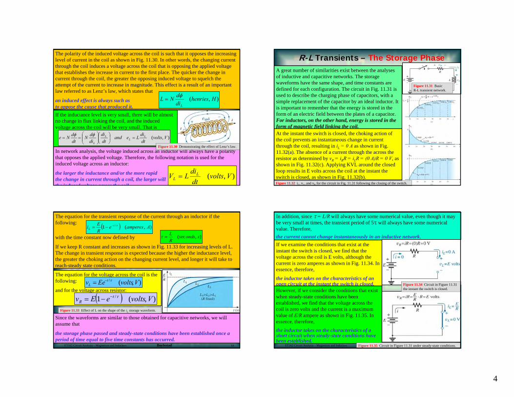
4
ET162 Circuit Analysis – Capacitors Boylestad 22
The polarity of the induced voltage across the coil is such that it opposes the increasing level of current in the coil as shown in Fig. 11.30. In other words, the changing current through the coil induces a voltage across the coil that is opposing the applied voltage that establishes the increase in current to the first place. The quicker the change in current through the coil, the greater the opposing induced voltage to squelch the attempt of the current to increase in magnitude. This effect is a result of an important law referred to as Lenz’s law, which states that
an induced effect is always such as to oppose the cause that produced it.
),( HhenriesdidNL
L
φ=
),( HhenriesdidNL
L
φ=
If the inductance level is very small, there will be almost no change in flux linking the coil, and the induced voltage across the coil will be very small. That is
In network analysis, the voltage induced across an inductor will always have a polarity that opposes the applied voltage. Therefore, the following notation is used for the induced voltage across an inductor:
the larger the inductance and/or the more rapidthe change in current through a coil, the larger will be the induced voltage across the coil
),( Vvoltsdtdi
LV LL =
),( Vvoltsdtdi
Leanddtdi
didN
dtdNe L
LL
L
=⎟⎠⎞
⎜⎝⎛⎟⎟⎠
⎞⎜⎜⎝
⎛==
φφ
Figure 11.30 Demonstrating the effect of Lenz’s law.
ET162 Circuit Analysis – Capacitors Boylestad 13
RR--LL Transients Transients –– The Storage PhaseThe Storage PhaseA great number of similarities exist between the analyses of inductive and capacitive networks. The storage waveforms have the same shape, and time constants are defined for each configuration. The circuit in Fig. 11.31 is used to describe the charging phase of capacitors, with a simple replacement of the capacitor by an ideal inductor. It is important to remember that the energy is stored in the form of an electric field between the plates of a capacitor. For inductors, on the other hand, energy is stored in the form of magnetic field linking the coil.
Figure 11.31 Basic R-L transient network.
At the instant the switch is closed, the choking action of the coil prevents an instantaneous change in current through the coil, resulting in iL = 0 A as shown in Fig. 11.32(a). The absence of a current through the across the resistor as determined by vR = iRR = iLR = (0 A)R = 0 V, as shown in Fig. 11.32(c). Applying KVL around the closed loop results in E volts across the coil at the instant the switch is closed, as shown in Fig. 11.32(b).Figure 11.32 iL, vL, and vR for the circuit in Fig. 11.31 following the closing of the switch.
The equation for the transient response of the current through an inductor if the following:
with the time constant now defined by
If we keep R constant and increases as shown in Fig. 11.33 for increasing levels of L. The change in transient response is expected because the higher the inductance level, the greater the choking action on the changing current level, and longer it will take to reach-steady state conditions.
The equation for the voltage across the coil is the following:
and for the voltage across resistor:
Since the waveforms are similar to those obtained for capacitive networks, we will assume that
the storage phase passed and steady-state conditions have been established once a period of time equal to five time constants has occurred.
( ) ),(1 / AampereseREi t
Lτ−−=
( ) ),(1 / VvoltseEv tR
τ−−=
),(/ VvoltsEev tL
τ−=
),(sec sondsRL
=τ
Figure 11.33 Effect of L on the shape of the iL storage waveform.
ET162 Circuit Analysis – Magnetism and Inductors Boylestad 14 ET162 Circuit Analysis – Magnetism and Inductors Boylestad 21
In addition, since τ = L/R will always have some numerical value, even though it may be very small at times, the transient period of 5τ will always have some numerical value. Therefore,the current cannot change instantaneously in an inductive network.If we examine the conditions that exist at the instant the switch is closed, we find that the voltage across the coil is E volts, although the current is zero amperes as shown in Fig. 11.34. In essence, therefore,
the inductor takes on the characteristics of an open circuit at the instant the switch is closed. Figure 11.34 Circuit in Figure 11.31
the instant the switch is closed.However, if we consider the conditions that exist when steady-state conditions have been established, we find that the voltage across the coil is zero volts and the current is a maximum value of E/R ampere as shown in Fig. 11.35. In essence, therefore,
the inductor takes on the characteristics of a short circuit when steady-state conditions have been established.
Figure 11.35 Circuit in Figure 11.31 under steady-state conditions.
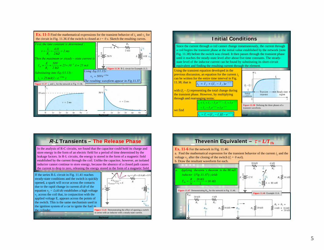
5
Ex. 11-3 Find the mathematical expressions for the transient behavior of iL and vL for the circuit in Fig. 11.36 if the switch is closed at t = 0 s. Sketch the resulting curves.
)emA(125i:Eq.(11.13)intongSubstituti
mA25A1025kΩ2V50
REI
iscurrentstatesteadyormaximumtheThen
ms2kΩ2H4
RLτ
:determinedisconstanttimetheFirst,
t/2msL
3
1m
1
−
−
−=
=×===
−
===
.37.11.FiginappearwaveformresultingTheVe50v
:Eq.(11.15)Usingt/2ms
L−=
Figure 11.36 R-L circuit for Example 11.3.
Figure 11.37 iL and vL for the network in Fig. 11.36.
ET162 Circuit Analysis – Magnetism and Inductors Boylestad 16 ET162 Circuit Analysis – Capacitors Boylestad 17
Initial ConditionsInitial ConditionsSince the current through a coil cannot change instantaneously, the current through a coil begins the transient phase at the initial value established by the network (note Fig. 11.38) before the switch was closed. It then passes through the transient phase until it reaches the steady-state level after about five time constants. The steady-state level of the inductor current can be found by substituting its short-circuit equivalent and finding the resulting current through the element.
Using the transient equation developed in the previous discussion, an equation for the current iLcan be written for the entire time interval in Fig. 11.38; that is
with (If – Ii) representing the total change during the transient phase. However, by multiplying through and rearranging terms:
we findττ
ττ
//
//
ti
tff
tii
tffiL
eIeII
eIIeIIIi−−
−−
+−=
+−−+=
τ/)( tfifL eIIIi −−+=
)1)(( /τtifiL eIIIi −−−+=
Figure 11.38 Defining the three phases of a transient waveform.
RR--LL Transients Transients –– The Release PhaseThe Release PhaseIn the analysis of R-C circuits, we found that the capacitor could hold its charge and store energy in the form of an electric field for a period of time determined by the leakage factors. In R-L circuits, the energy is stored in the form of a magnetic fieldestablished by the current through the coil. Unlike the capacitor, however, an isolated inductor cannot continue to store energy, because the absence of a closed path causes the current to drop to zero, releasing the energy stored in the form of a magnetic field.
If the series R-L circuit in Fig. 11.41 reaches steady-state conditions and the switch is quickly opened, a spark will occur across the contacts due to the rapid change in current di/dt of the equation vL = L(di/dt) establishes a high voltage vL across the coil that, in conjunction with the applied voltage E, appears across the points of the switch. This is the same mechanism used in the ignition system of a car to ignite the fuel in the cylinder. Figure 11.41 Demonstrating the effect of opening a switch
in series with an inductor with a steady-state current.
ET162 Circuit Analysis – Magnetism and Inductors Boylestad 18 ET162 Circuit Analysis – Capacitors Boylestad 19
Thevenin Equivalent – τ = L/TTh
Ex. 11-6 For the network in Fig. 11.46:a. Find the mathematical expression for the transient behavior of the current iL and the voltage vL after the closing of the switch (Ii = 0 mA).b. Draw the resultant waveform for each.
Figure 11.46 Example 11.6.
Ω=Ω
== kkNRT
yieldsFiginductormHthetotheoremstheveninApplyinga
Th 102
20)47.11.(
80'.
Figure 11.47 Demonstrating RTh for the network in Fig. 11.46.
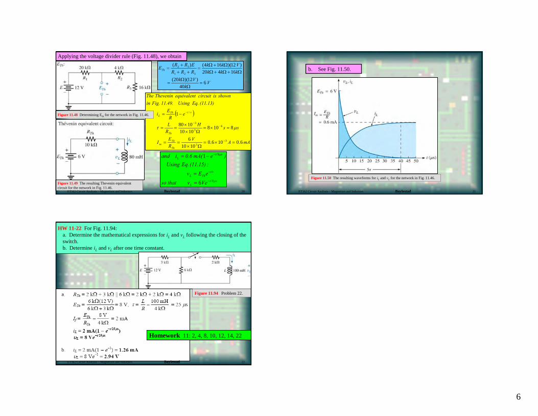
6
Applying the voltage divider rule (Fig. 11.48), we obtain
Vk
VkkkkVkk
RRRERR
ETh
640
)12)(20(16420
)12)(164()(
321
32
=Ω
Ω=
Ω+Ω+ΩΩ+Ω
=++
+=
( )
mAAVRE
I
ssHRL
eR
Ei
(11.13)Eq.Using11.49.Fig.inshowniscircuitequivalentTheveninThe
Th
Thm
Th
τtThL
6.0106.01010
6
810810101080
1
33
63
3
/
=×=Ω×
==
=×=Ω×
×==
−=
−
−−
−
µτ
µst/L
t/τThL
µst/L
Vevthatso
eEv:(11.15)Eq.Using
)emA(0.6iand
8
8
6
1
−
−
−
=
=
−=
Figure 11.49 The resulting Thevenin equivalent circuit for the network in Fig. 11.46.
Figure 11.48 Determining Eth for the network in Fig. 11.46.
ET162 Circuit Analysis – Magnetism and Inductors Boylestad 20 ET162 Circuit Analysis – Magnetism and Inductors Boylestad 21
Figure 11.50 The resulting waveforms for iL and vL for the network in Fig. 11.46.
b. See Fig. 11.50.
HW 11-22 For Fig. 11.94:a. Determine the mathematical expressions for iL and vL following the closing of the switch.b. Determine iL and vL after one time constant.
Homework 11: 2, 4, 8, 10, 12, 14, 22
Figure 11.94 Problem 22.
ET162 Circuit Analysis – Magnetism and Inductors Boylestad 22
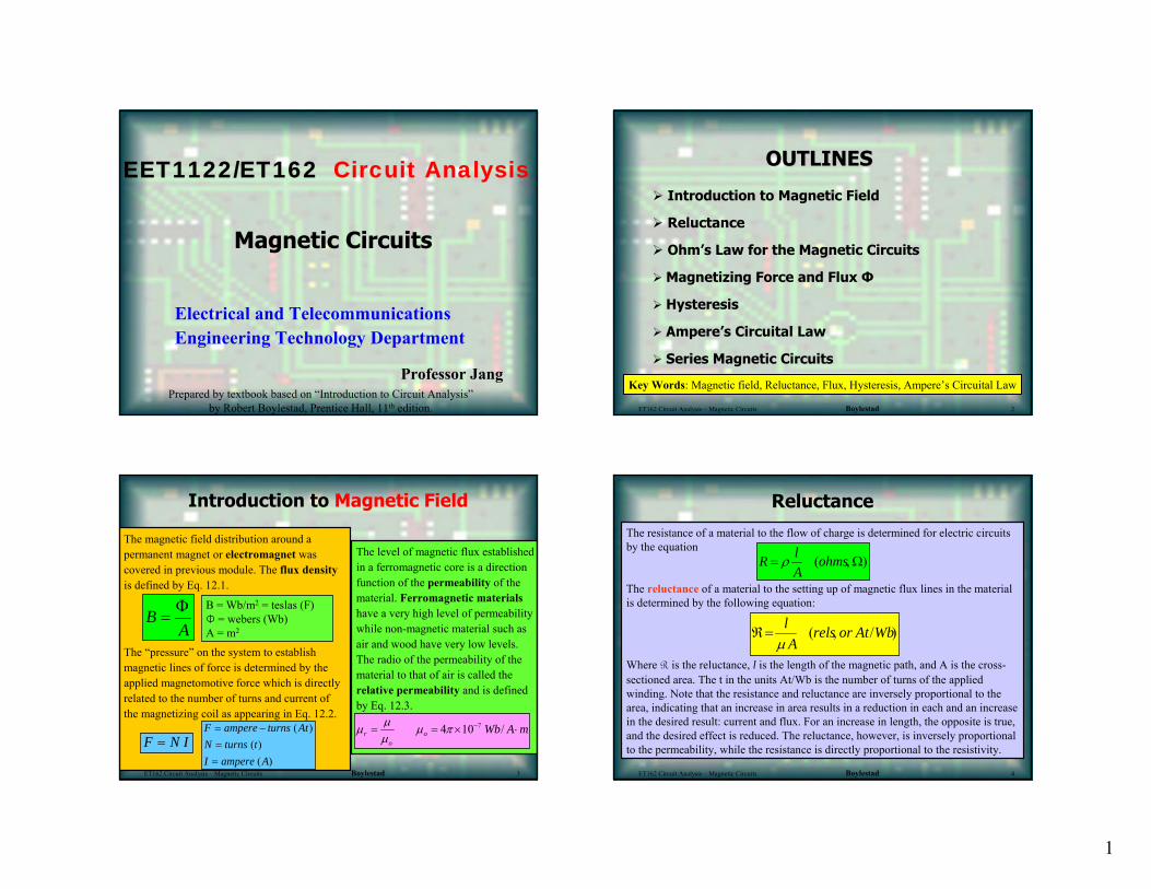
1
Magnetic Circuits
EET1122/ET162 Circuit Analysis
Electrical and Telecommunications Engineering Technology Department
Professor JangPrepared by textbook based on “Introduction to Circuit Analysis”
by Robert Boylestad, Prentice Hall, 11th edition.
OUTLINESOUTLINES
Introduction to Magnetic Field
Reluctance
Ohm’s Law for the Magnetic Circuits
Hysteresis
Magnetizing Force and Flux Φ
Key Words: Magnetic field, Reluctance, Flux, Hysteresis, Ampere’s Circuital Law
ET162 Circuit Analysis – Magnetic Circuits Boylestad 2
Ampere’s Circuital Law
Series Magnetic Circuits
Introduction to Magnetic Field
The magnetic field distribution around a permanent magnet or electromagnet was covered in previous module. The flux densityis defined by Eq. 12.1.
The “pressure” on the system to establish magnetic lines of force is determined by the applied magnetomotive force which is directly related to the number of turns and current of the magnetizing coil as appearing in Eq. 12.2.
The level of magnetic flux established in a ferromagnetic core is a direction function of the permeability of the material. Ferromagnetic materialshave a very high level of permeability while non-magnetic material such as air and wood have very low levels. The radio of the permeability of the material to that of air is called the relative permeability and is defined by Eq. 12.3.
B = Wb/m2 = teslas (F)Φ = webers (Wb)A = m2
)()(
)(
AampereItturnsN
AtturnsampereF
==
−=
AB Φ=
INF =mAWbo
or ⋅×== − /104 7πµ
µµµ
ET162 Circuit Analysis – Magnetic Circuits Boylestad 3
ReluctanceThe resistance of a material to the flow of charge is determined for electric circuits by the equation
The reluctance of a material to the setting up of magnetic flux lines in the material is determined by the following equation:
Where R is the reluctance, l is the length of the magnetic path, and A is the cross-sectioned area. The t in the units At/Wb is the number of turns of the applied winding. Note that the resistance and reluctance are inversely proportional to the area, indicating that an increase in area results in a reduction in each and an increase in the desired result: current and flux. For an increase in length, the opposite is true, and the desired effect is reduced. The reluctance, however, is inversely proportional to the permeability, while the resistance is directly proportional to the resistivity.
)/,( WbAtorrelsA
lµ
=ℜ
),( Ω= ohmsAlR ρ
ET162 Circuit Analysis – Magnetic Circuits Boylestad 4
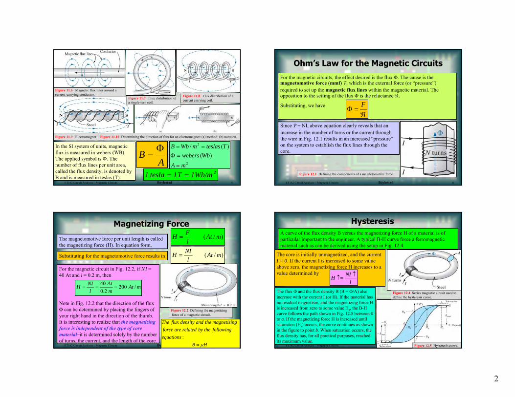
2
In the SI system of units, magnetic flux is measured in webers (WB). The applied symbol is Φ. The number of flux lines per unit area, called the flux density, is denoted by B and is measured in teslas (T).
Figure 11.6 Magnetic flux lines around a current-carrying conductor.
Figure 11.7 Flux distribution of a single-turn coil.
Figure 11.8 Flux distribution of a current carrying coil.
Figure 11.9 Electromagnet. Figure 11.10 Determining the direction of flux for an electromagnet: (a) method; (b) notation.
AB Φ=
2
2
)()(/
mAWbwebers
TteslasmWbB
=
=Φ==
2Wb/m1T1tesla1 ==ET162 Circuit Analysis – Magnetic Circuits Boylestad 5
OhmOhm’’s Law for the Magnetic Circuitss Law for the Magnetic Circuits
For the magnetic circuits, the effect desired is the flux Φ. The cause is themagnetomotive force (mmf) F, which is the external force (or “pressure”) required to set up the magnetic flux lines within the magnetic material. The opposition to the setting of the flux Φ is the reluctance R.
Substituting, we have
Figure 12.1 Defining the components of a magnetomotive force.
ℜ=Φ
F
Since F = NI, above equation clearly reveals that an increase in the number of turns or the current through the wire in Fig. 12.1 results in an increased “pressure”on the system to establish the flux lines through the core.
ET162 Circuit Analysis – Magnetic Circuits Boylestad 6
ET162 Circuit Analysis – Magnetic Circuits Boylestad 7
Substituting for the magnetomotive force results in
Magnetizing Force)/( mAt
lFH =
)/( mAtl
NIH =
The magnetomotive force per unit length is called the magnetizing force (H). In equation form,
For the magnetic circuit in Fig. 12.2, if NI = 40 At and l = 0.2 m, then
Note in Fig. 12.2 that the direction of the flux Φ can be determined by placing the fingers of your right hand in the direction of the thumb. It is interesting to realize that the magnetizing force is independent of the type of core material–it is determined solely by the number of turns, the current, and the length of the core.
HBequations
followingthebyrelatedareforcegmagnetizintheanddensityfluxThe
µ=:
mAtmAt
lNIH /200
2.040
===
Figure 12.2 Defining the magnetizingforce of a magnetic circuit.
ET162 Circuit Analysis – Magnetic Circuits Boylestad 2
HysteresisA curve of the flux density B versus the magnetizing force H of a material is of particular important to the engineer. A typical B-H curve force a ferromagnetic material such as can be derived using the setup in Fig. 12.4.
The core is initially unmagnetized, and the current I = 0. If the current I is increased to some value above zero, the magnetizing force H increases to a value determined by
lNIH ↑
↑=
The flux Φ and the flux density B (B = Φ/A) also increase with the current I (or H). If the material has no residual magnetism, and the magnetizing force H is increased from zero to some value Ha, the B-H curve follows the path shown in Fig. 12.5 between 0to a. If the magnetizing force H is increased until saturation (Hs) occurs, the curve continues as shown in the figure to point b. When saturation occurs, the flux density has, for all practical purposes, reached its maximum value.
Figure 12.4 Series magnetic circuit used to define the hysteresis curve.
Figure 12.5 Hysteresis curve.
3
If the entire cycle is repeated, the curve obtained for the same core will be determined by the maximum H applied. Three hysteresis loops for the same material for maximum values of H less than the saturation value are shown in Fig. 12.6. In addition, the saturation curve is repeated for comparison purposes.
If the magnetizing force is reduced to zero by letting I decrease to zero, the curve follows the path of the curve follows the path of the curve between b and c. The flux density BR, which remains when the magnetizing force is zero, is called the residual flux density. It is this residual flux density that makes it possible to create permanent magnets. If the current I is reserved, developing a magnetizing force, –H, the flux density when –Hd is reached. The magnetizing force –Hd required to “coerce” the flux density to reduce its level to zero is called the coercive force. As the force –H is increased until saturation again occurs and is then reserved and brought back to zero, the path def results. If the magnetizing force is increased in the positive direction (+H), the curve traces the path shown from f to b. the entire curve represented by bcdefb is called the hysteresis curve.
Figure 12.4 Defining the normal magnetization curve.ET162 Circuit Analysis – Magnetic Circuits Boylestad 9
The similarity between the analyses of electric and magnetic circuits has been demonstrated to some extent for the quantities in Table 12.1.
Table 12.1If we apply the “cause” analogy to KCL (∑ V = 0), we obtain the following:
∑ F = 0 (for magnetic Circuits)
which, in words, states that the algebraic sum of the rises and drops of the mmf around a closed loop of a magnetic circuits is equal to zero.
Ampere’s Circuital Law
RROpposition
ΦIEffect
FECause
Magnetic Circuits
Electric Circuit
Above equation is referred as Ampere’s circuital law. When it is applied to magnetic circuits, sources of mmf are expressed by the equation
F = NI (At)
The equation for the mmf drop across a portion of a magnetic circuit can be found by applying the relationships listed in Table 12.1; that is, for electric circuits,
V = IR
Resulting in the following for magnetic circuitsF = ΦR (At)
Where Φ is the flux passing through a section of the magnetic circuit and R is the reluctance of that section. A more practical equation for the mmfdrop is,
F = H l (At)
where H is the magnetizing force on a section of a magnetic circuit and l is the length of the section.
Flux ΦIf we continue to apply the relationships described in the previous module to KCL, we find that the sum of the fluxes entering a junction is equal to the sum of the fluxes leaving a junction; that is, for the circuit in Fig. 12.11,
both of which are equivalent.Figure 12.11 Flux distribution of a series-parallel magnetic network.
)()(
bjunctionatorajunctionat
acb
cba
Φ=Φ+ΦΦ+Φ=Φ
Series Magnetic Circuits – Determining NIIn one type, Φ is given, and the impressed mmf NI must be computed. This is the type of problem encountered in the design of motors, generators, and transformers. In the other type, NI is given, and the flux Φ of the magnetic circuit must be found. This type of problem is encountered primarily in the design of magnetic amplifiers. This section considers only series magnetic circuits in which the flux Φ is the same throughout.
ET162 Circuit Analysis – Magnetic Circuits Boylestad 11
Using the B-H curves in Fig. 12.8, we can determine the magnetizing force H:
H (cast steel) = 170 At/m
Applying Ampere’s circuital law yields
NI = Hl
and
TTmWb
AB
isBdensityfluxThea
2.0102102104
.
123
4
=×=××
== −−
−φ
mAt
mmAtN
lHI 68400
)16.0)(/170(===
Figure 12.12 Example 12.1.
The magnetic circuit can be represented by the system shown in Fig. 12.13(a). The electric circuit analogy is shown in Fig. 12.13(b). Analogies of this type can be very helpful in the solution of magnetic circuits. Table 12.2 is for part (a) of this problem.
Ex. 12-1 For the series magnetic circuit in Fig. 12.12:a. Find the value of I required to develop a magnetic flux of Φ = 4×10⁻⁴ Wb.b. Determine µ and µr for the material under these conditions.
ET162 Circuit Analysis – Magnetic Circuits Boylestad 12
4
Figure 12.13 (a) magnetic circuit equivalent and (b) electric circuit analogy.
83.935104
10176.1
/10176.1/170
2.0.
7
3
3
=××
==
⋅×===
−
−
−
πµµµ
µ
os
istypermeabilirelativetheand
mAWbmAt
THB
foundbecanmaterialtheoftypermeabiliTheb
0.162×10-34×10-4One continuous section
Hl(At)l(m)H(At/m)B(T)A(m2)Φ (Wb)SectionTable 12.1
ET162 Circuit Analysis – Magnetic Circuits Boylestad 13
Air GapsLet’s consider the effects that an air gap has on a magnetic circuit. Note the presence of air gaps in the magnetic circuits of the motor and meter in Fig. 11.15. The spreading of the flux lines outside thecommon area of the core for the air gap in Fig. 12.18(a) is known as fringing. For our purposes, we shall ignore this effect and assume the flux distribution to be as in Fig. 12.18(b).
The flux density of the air gap in Fig. 12.18(b) is given by
where, for our purposes,
andcoreg
coreg
AA =
Φ=Φ
g
gg A
BΦ
=
For the most practical applications, the permeability of air is taken to be equal to that of free space. The magnetizing force of the air gap is then determined by
o
gg
BH
µ=
and the mmf drop across the air gap is equal to HgLg. An equation for Hg is as follows:
)/()1096.7(104
5
7
mAtBHand
BBH
gg
g
o
gg
×=
×== −πµ
Figure 12.18 Air gap: (a) with fringing; (b) ideal.
ET162 Circuit Analysis – Magnetic Circuits Boylestad 14
ET162 Circuit Analysis – Magnetism and Inductors Boylestad 21
An equivalent magnetic circuit and its electric circuit analogy are shown in Fig. 12.20.
The flux density for each section is
From the B-H curves in Fig. 12.28,
Ex. 12-4 Find the value of I required to establish a magnetic flux of Φ = 0.75 × 10⁻⁴
Wb in the series magnetic circuit in Fig. 12.19.
Figure 12.19 Relay for Example 12.4.mAtsteelcastH /280)( ≅
TmWb
AB 5.0
105.11075.0
24
4
=××
=Φ
= −
−
Applying Equation,
The mmf drops are
Applying Ampere’s circuital law,
mAtTBH gg /1098.3)5.0)(1096.7()1096.7( 555 ×=×=×=
AtmmAtIH
AtmmAtIH
gg
corecore
796)102)(/1098.3(
28)10100)(/280(35
3
=××=
=×=−
−
AIandAtI
AtAtIHIHNI ggcorecore
12.4824)200(
79628
==
+=+=
Figure 12.20 (a) Magnetic circuit equivalent and (b) electric circuit analogy for the relay in Fig. 12.19.
HW 12-6 Repeat Problem 5 for Φ = 72,000 maxwells and an impressed mmf of 120 gilberts.
Homework 12: 2, 4, 6, 12-14.ET162 Circuit Analysis – Magnetic Circuits Boylestad 16
)(1067.1max000,72
120 3 CGSrelswells
gilberts −×==Φℑ
=ℜ


![Circuit Network Analysis - [Chapter1] Basic Circuit Laws](https://img.pdfslide.us/doc/110x75/55ced242bb61eb192c8b480c/circuit-network-analysis-chapter1-basic-circuit-laws.jpg)