Embed Size (px)
Citation preview

Progress In Electromagnetics Research C, Vol. 25, 133–144, 2012
AN ULTRA-WIDEBAND BALANCED BANDPASS FIL-TER BASED ON DEFECTED GROUND STRUCTURES
B. Xia1, 2, *, L.-S. Wu2, and J. F. Mao2
1Zhenjiang Watercraft College PLA, Zhenjiang, Jiangsu 212003, China2Key Lab of Ministry of Education for Research of Design and EMCof High Speed Electronic Systems, Shanghai Jiao Tong University,Shanghai 200240, China
Abstract—An ultra-wideband (UWB) balanced bandpass filter(BPF) is proposed and designed using defected ground structures(DGSs). A multimode resonator on top layer with a coplanarwaveguide on bottom layer is used to design a UWB BPF. U-shapedand H-shaped DGSs loaded with capacitor are used to design toprovide common mode rejection within a lower band, while a set ofdumbbell-shaped DGSs are utilized to provide common mode rejectionwithin an upper-band. The proposed UWB balanced BPF shows theperformance of good common mode rejection in and out of the UWBpassband.
1. INTRODUCTION
With the development of fully-integrated balanced transceiver,differential-mode operation exhibits much higher immunity to noisethan single-ended signaling. Much effort has been made to developvarious balanced filters to meet the requirement of common-modesuppression in modern high-speed communication systems.
In [1], a balanced bandpass filter (BPF) is implemented withbalanced coupled-line structures. In [2], half- and quarter-wavelengthstepped-impedance resonators (SIRs) are utilized to realize dual-bandbalanced BPF. Both the two balanced BPFs have narrow differential-mode passband and wide common-mode suppression band. Thecenter loading technique is proposed to further improve the common-mode suppression characteristic for narrowband BPFs [3]. In [4], a
Received 25 August 2011, Accepted 8 November 2011, Scheduled 14 November 2011* Corresponding author: Bin Xia ([email protected]).

134 Xia, Wu, and Mao
compact second-order differential bandpass filter is presented. Thetransformer structure is integrated using integrated passive device(IPD) technology on a glass substrate to achieve compact circuit areaand system-in-package (SiP) applications. In [5], a very compactdifferential bandpass filter was designed with improved high-frequencyrejection, suitable for SiP circuit integration.
Ultra-wideband (UWB) technique has drawn much attention forvarious applications [6–9]. A two-stage differential-mode BPF isdesigned using symmetrical bisections of branch-line topology [10]. Asix-stage UWB differential-mode BPF is implemented [11], but withpoor performance of in-band insertion loss. In [12], the equivalent3λ/4 short-ended stub is introduced into a wideband differential-modeBPF to achieve good frequency selectivity. In [10–12], however, thecommon-mode suppression in stopband is not good, and the out-of-band common-mode noise would still produce possible electromagneticinterference (EMI) problem for wireless application. In [13], an UWBdifferential filter is developed with good performance of differential-mode propagation and common-mode suppression, which is basedon the structure of double-side parallel-strip line (DSPSL). However,in order to incorporate the DSPSL structure into widely usedmicrostrip circuit, additional transitions are needed to accomplish theirconnection, which may take more area and introduce more losses.
In this article, a novel UWB balanced BPF is proposed with a pairof symmetrical UWB filtering units based on differential transmissionlines. To improve its performance of common-mode suppression,dumbbell-, U- and H-shaped defected ground structures (DGSs) areintroduced to reject the common-mode propagation from DC to18GHz. The good performance of our proposed UWB balanced BPFwith DGSs has been demonstrated by the agreement obtained betweenthe simulated and measured S-parameters.
2. ANALYSIS AND DESIGN
The top and bottom views of the proposed UWB balanced BPF areshown in Figs. 1(a) and (b), respectively. It is mainly composed ofthree parts. The first part is a pair of UWB filtering units designedfor differential transmission lines. The second part is built up by twoU-shaped DGSs and an H-shaped one loaded with a capacitor. Thesethree etched structures provide the rejection of common-mode noisewithin the lower band of UWB. The third part consists of a set ofdumbbell-shaped DGSs to suppress the common-mode noise in upperband of UWB. Odd mode impedance of differential line matchingto 50 Ω, and is computed by the methods about coupled microstrip

Progress In Electromagnetics Research C, Vol. 25, 2012 135
4 3
(a) (b)
Figure 1. Configuration of the proposed UWB balanced BPF. (a) Itstop view, and (b) bottom view.
C1 C2 C2 C2 C1 L 5
L1 L2 L2 L2 L1
0Z eZ eZ eZ eZ eZ
m1k m2k m1km2k
eZ
C6C6
C5
C3
C
C4 C3
m3km4k
m3k
eZ eZ eZ eZ 0Z
L 3 L4 L 3
a
Figure 2. The common mode equivalent lumped model.
without considering DGS, that is because DGS has little influence onodd mode impedance in passband. Even mode impedance mismatchwith 50 Ω, mismatching benefit to suppress common mode noise, theDGS of Sections 2 and 3 suppress mainly common mode noise. So,even mode impedance may not need to be considered.
2.1. Theoretical Model and Parameters Extraction
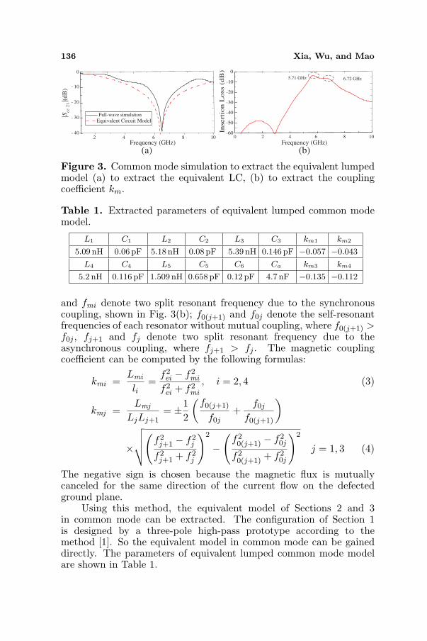
In [14], a method is used to extract the equivalent model of commonmode response. The common mode equivalent lumped model ofthe proposed configuration is shown in Fig. 2. The common modesimulation results of each resonator can be matched to the one-poleButterworth type low-pass response, which has 3-dB cutoff frequencyin Fig. 3(a). Cp and Lp denote the gap capacitance between two sidesof the slit and the equivalent inductance of the signal passing throughthe one DGS resonating unit. The extracted LC equivalent circuit canbe found in [15] and are given bellow.
Cp =fc
4πZc
(1
f20 − f2
c
)(1)
L =1
4π2f20 Cp
(2)
The mutual coupling is synchronous for two identical U-shapedor H-shaped resonators or identical dumb bell shaped resonator andis asynchronous between U- and H-shaped resonators or between un-identical dumb bell shaped resonators due to geometrical asymmetry.The magnetic coupling between any two resonators is dominant, fei
136 Xia, Wu, and Mao
2 4 6 8- 40
- 30
- 20
- 10
0
|Scc
21|(
dB
)
-60
-50
-40
-30
-20
-10
0
2 4 6 810 100
Frequency (GHz) Frequency (GHz)
Inse
rtio
n L
oss
(d
B)
Full-wave simulationEquivalent Circuit Model
5.71 GHz 6.72 GHz
(a) (b)
Figure 3. Common mode simulation to extract the equivalent lumpedmodel (a) to extract the equivalent LC, (b) to extract the couplingcoefficient km.
Table 1. Extracted parameters of equivalent lumped common modemodel.
L1 C1 L2 C2 L3 C3 km1 km2
5.09 nH 0.06 pF 5.18 nH 0.08 pF 5.39 nH 0.146 pF −0.057 −0.043
L4 C4 L5 C5 C6 Ca km3 km4
5.2 nH 0.116 pF 1.509 nH 0.658 pF 0.12 pF 4.7 nF −0.135 −0.112
and fmi denote two split resonant frequency due to the synchronouscoupling, shown in Fig. 3(b); f0(j+1) and f0j denote the self-resonantfrequencies of each resonator without mutual coupling, where f0(j+1) >f0j , fj+1 and fj denote two split resonant frequency due to theasynchronous coupling, where fj+1 > fj . The magnetic couplingcoefficient can be computed by the following formulas:
kmi =Lmi
li=
f2ei − f2
mi
f2ei + f2
mi
, i = 2, 4 (3)
kmj =Lmj
LjLj+1= ±1
2
(f0(j+1)
f0j+
f0j
f0(j+1)
)
×
√√√√(
f2j+1 − f2
j
f2j+1 + f2
j
)2
−(
f20(j+1) − f2
0j
f20(j+1) + f2
0j
)2
j = 1, 3 (4)
The negative sign is chosen because the magnetic flux is mutuallycanceled for the same direction of the current flow on the defectedground plane.
Using this method, the equivalent model of Sections 2 and 3in common mode can be extracted. The configuration of Section 1is designed by a three-pole high-pass prototype according to themethod [1]. So the equivalent model in common mode can be gaineddirectly. The parameters of equivalent lumped common mode modelare shown in Table 1.

Progress In Electromagnetics Research C, Vol. 25, 2012 137
(a) (b) (c)
0 5 10 15 20
-60
-40
-20
0
Sdd 21
Scc 21
Sdd 2
1 / S
cc 2
1 (dB
)
Frequency (GHz)
Figure 4. UWB filtering part of the balanced filter. (a) Its top view,(b) bottom view, and (c) the simulated S-parameters for differentialand common modes. (W1 = 0.56mm, W2 = 1.27mm, W3 = 2.53mm,W4 = 0.36 mm, W5 = 0.92 mm, W6 = 4.3 mm, W7 = 3.5mm, W8 =0.4mm, L1 = 0.36 mm, L2 = 1.3mm, L3 = 0.62mm, L4 = 0.27mm,L5 = 0.4mm, L6 = 3.2mm, and L7 = 4.0mm.)
2.2. UWB Filtering Units for Differential Lines
As shown in Fig. 4, the UWB filtering part of our component containstwo symmetrical units. Each unit is constructed by a pair of multimoderesonators with a coplanar waveguide structure beneath them [15],which is utilized to provide a UWB bandpass characteristic for asingle line of the differential pair. With this part, the UWB bandpassresponse with two transmission zeros is obtained for the differentialmode. Obviously, the two UWB filtering units are independent witheach other. Thus, the common-mode response is similar to thedifferential-mode one, as shown in Fig. 4(c). The relative permittivityof εr = 4.3, the loss tangent of tan δ = 0.003, and the thickness ofh = 0.41mm. As shown in [14], the common-mode suppression levelof UWB structure below 3 GHz is near 0 dB.
2.3. U- and H-Shaped DGSs for Lower Band Common-modeSuppression
In [14], U- and H-shaped DGSs are etched on the ground planeto suppress common-mode noise for GHz differential lines. Similarstructures are utilized to improve the lower band common-moderejection characteristic as the second part of the balanced filter, asshown in Fig. 5(a). This part consists of two U-shaped DGS resonatorsand an H-shaped one operating at lower band. The simulationof this part without capacitor loaded presents poor common modesuppression in lower passband as in [14]. Because ultra-wide stop-

138 Xia, Wu, and Mao
0 5 10 15 20-70
-60
-50
-40
-30
-20
-10
0
S dd
21/
Scc 2
1(d
B)
0 5 10 15 20
-60
-40
-20
0
Sd
d 2
1 /
Sc
c 2
1 (G
Hz
)
Frequency (GHz)
Sdd 21
Scc 21
GHz
Sdd 21
Scc 21
(a) (b) (c)
Figure 5. First and second parts of the balanced UWB BPF. (a) Theconfiguration, and (b) the simulated results without capacitor. (c) Thesimulated results with capacitor. (W9 = 8.0mm, W10 = 1.9mm,W11 = 1.2mm, W12 = 1.0mm, W13 = 1.4 mm, L8 = 1.0mm, L9 =5.0mm, L10 = 9.4mm, L11 = 1.0mm, L12 = 2.2mm, L13 = 1.92mm,L14 = 0.36mm, L15 = 0.3mm, and L16 = 1.12mm).
(a)
(b) (c)
P1 P2
Figure 6. The differential response of DGS resonator in the Section 3.(a) The configuration, (b) the equivalent model, and (c) simulation.
band of common mode response is affected by resonation frequency ofthree LC resonator of UH-shaped DGS’s equivalent circuit, and theresonation frequency of three LC resonator is affected by size of UH-shaped DGS. The wanted common mode rejection of lower-band ofUWB needs lower resonation frequency of equivalent LC resonator,the lower resonation frequency of equivalent LC resonator needs largersize of DGS. To improve the common mode suppression in lower bandand miniaturize the H-shaped DGS, a capacitor of 4.7 nF is loaded atits center. The simulated response of the first two parts is plotted inFig. 5(c), with the optimized geometrical parameters also given.
The DGS resonators are seemed to be shorted to electric wallin differential mode response. The DGS resonators in Section 2 actmainly as two coupling bypass half-wavelength resonators shortedat two ends. The Section 2 with DGS resonators can be seemed

Progress In Electromagnetics Research C, Vol. 25, 2012 139
as two poles bandstop filter. The Fig. 6(c) presents the simulationresults conforming to our analysis. The bandstop frequency is around12.5GHz.
2.4. Dumbbell-Shaped DGSs for Upper BandCommon-mode Suppression
Patterned structure on top layer or ground is usually used to improvebandstop performance [16, 17]. In order to improve the performanceof upper band common-mode suppression, a set of dumbbell-shapedDGS unit cells is designed as the third part of the proposed UWBbalanced filter. As shown in Fig. 7(a), the dumbbell-shaped etchedpatterns [18] are located under both the two differential lines. Thedominant mode of the DGS resonators is an even-mode, so they canprovide a stopband at the dominant resonant frequency for the commonmode. And their second resonant mode is an odd-mode, which willalso produce a stopband at the second resonant frequency for thedifferential mode. Fig. 7(b) shows the optimized S-parameters of thecascading of the first and third parts of the proposed component. It isfound that the common-mode suppression is achieved within not onlythe upper band of UWB but also the upper stopband, and the out-of-band rejection is also improved above 17GHz for the differential modefilter.
The DGS resonators in Section 3 act mainly as four couplingbypass half-wavelength resonators shorted at two ends. The Section 3with DGS resonators can be seemed as four poles bandstop filter(Figs. 8(a), (b)). The Fig. 8(c) presents the simulation resultsconforming to our analysis. The bandstop frequency is around 17 GHz.
0 5 10 15 2 0
-6 0
-4 0
-2 0
0
S dd 21
S cc 21
Sdd
21 / S
cc
21 (
GH
z)
Frequency (GHz)
22L
21L
(a) (b)
Figure 7. First and third parts of the balanced UWB BPF. (a) Theconfiguration, and (b) the simulated results. (W14 = 2.0mm, W15 =3.0mm, L17 = 2.0 mm, L18 = 0.4mm, L19 = 0.3mm, L20 = 0.4mm,L21 = 10 mm, L22 = 0.88mm).

140 Xia, Wu, and Mao
(a)
(b) (c)
Figure 8. The differential response of DGS resonator in the Section 3.(a) The configuration, (b) the equivalent model, and (c) simulation.
(a) (b)
Figure 9. Photo of the fabricated filter prototype. (a) Its top view,and (b) bottom view.
The DGS resonators in Sections 2 and 3 provide two bandstop around12.5GHz and 17GHz, which benefit the differential mode bandstopperformance.
It is easy to understand that the common-mode suppression in thewhole frequency range of interest can be implemented by using the U-/H-shaped DGSs and dumbbell-shaped ones together with the UWBfiltering units, while the UWB bandpass characteristic of differentialmode will not be degraded. So the proposed UWB balanced bandpassfilter is a cascade of the three parts, as shown in Fig. 1.
3. RESULTS AND DISCUSSION
To validate our idea, a filter prototype is designed and fabricated on aTaconic TRF-43 substrate, with the relative permittivity of εr = 4.3,the loss tangent of tan δ = 0.003, and the thickness of h = 0.41mm, asshown in Fig. 9. The overall size of the prototype is 26.2× 11.9mm2.
The balanced filter, as a four-port component, is measured byAgilent 8722ES vector network analyzer. Then, its S-parameters ofdifferential and common modes are extracted by
Sdd21 = S21 − S31 (5)Scc21 = S21 + S31 (6)

Progress In Electromagnetics Research C, Vol. 25, 2012 141
|Sdd|
|Scc|
5 10 1-100
-80
-60
-40
-20
0In
sert
ion
lo
ss (
dB
)
Frequency(GHz)
Simulated Measured Equivelent lumped model
2 4 6 8 100.0
0.2
0.4
0.6
0.8
Sdd
21
Gro
up d
elay
(ns)
Frequency (GHz)
Simulated Measured
125
(a) (b)
Figure 10. Insertion loss and group delay of the UWB balanced filter,(a) insertion loss, (b) group delay.
Table 2. Comparison to other published differential-mode ultrawideband filter.
Ref [4] [5] [6] [7] this work
frequecy range inmeasurement 1-8 GHz 1-13 GHz 0-9 GHz 0-8 GHz 0-18 GHz
differential modepassband
2.7-5.3 GHz
2.9-10.7 GHz
2.8-5.3 GHz
1.6-4.37 GHz
3.54-10.6 GHz
differential modepassband insertion 0.5-2 dB 0.5-7dB 0.5-2.5
dB1.19-2.05dB
0.11-2.50dB
common modesuppression
level (passband)>20 dB >14 dB >17 dB >20 dB >20 dB
common modesuppression
level (lowerstopband)
0-20 dB 0-20 dB 0-20 dB >20 dB >14.3 dB
common modesuppression
level (upperstopband)
0-20 dB 0-20 dB 0-20 dB >5 dB >15.4 dB
compatible withmicrostrip yes yes yes No yes
The extracted S-parameters of the prototype are plotted inFig. 10(a), with its simulated results also provided for comparison.Good agreement is obtained between them. From 3.54 to 11.30GHz,the insertion loss of differential mode is from 0.11 to 2.5 dB. Theextracted 3-dB bandwidth of differential mode is from 3.52 to

142 Xia, Wu, and Mao
11.40GHz, slightly narrower than the simulated one from 3.24 to11.67GHz. The rejection level of common mode is better than 20 dBfrom 3.28 to 10.96 GHz in measurement, while the simulated 20-dBrejection band is from 3.51 to 10.98 GHz. The extracted common-mode suppressions in the lower and upper stopbands are better than14.3 and 15.4 dB, respectively. As shown in Table 2, this work can notonly directly connect to microstrip circuits but also suppress commonmode noise to 14.3 dB both in lower and upper stopband. Fig. 10(b)shows the group delay of simulated and measured results. It is foundthe measured group delay is about 0.54 ns and the simulated groupdelay is about 0.46 ns at center frequency. The group delay is plain inpass band and almost not degraded within the passband.
4. CONCLUSION
In this work, a new UWB balanced BPF based on DGSs is designed.Since each differential line can act as the return path of current forthe other one, the DGSs etched below the differential lines have littleinfluence on the differential-mode response. The differential-mode andcommon-mode responses of the proposed component can be designedindividually. The UWB bandpass characteristics for both modes areprovided by a pair of multimode resonators on the top layer with twocoplanar waveguides on bottom layer. The U-/H-shaped DGSs loadedwith a capacitor and dumbbell-shaped ones suppress the common-mode noise within the whole frequency range of interest. The proposedUWB balanced BPF has a good performance of wideband common-mode suppression, which is demonstrated by the good agreementobtained between its measured and simulated S-parameters.
ACKNOWLEDGMENT
This work was supported by the National Basic Research Program ofChina under Grant of 2009CB320202, by the National Natural ScienceFoundation of China under Grant of 60821062, and by the NationalNatural Science Foundation of China under Grant of 61001014.
REFERENCES
1. Wu, C.-H., C.-H. Wang, and C. H. Chen, “Novel balanced coupled-line bandpass filters with common-mode noise suppression,” IEEETrans. on Microw. Theory and Tech., Vol. 55, No. 2, 287–295,Feb. 2007.

Progress In Electromagnetics Research C, Vol. 25, 2012 143
2. Shi, J. and Q. Xue, “Novel balanced dual-band bandpass filterusing coupled stepped-impedance resonators,” IEEE Microw.Wireless Compon. Lett., Vol. 20, No. 1, 19–21, Jan. 2010.
3. Shi, J. and Q. Xue, “Balanced bandpass filters using center-loadedhalf-wavelength resonators,” IEEE Trans. on Microw. Theory andTech., Vol. 58, No. 4, 970–977, Apr. 2010.
4. Wu, S.-M., C.-T. Kuo, and C.-H. Chen, “Very compact full dif-ferential bandpass filter with transformer integrated using inte-grated passive device technology,” Progress In ElectromagneticsResearch, Vol. 113, 251–267, 2011.
5. Wu, S.-M., C.-T. Kuo, P.-Y. Lyu, Y.-L. Shen, and C.-I. Chien,“Miniaturization design of full differential bandpass filter withcoupled resonators using embedded passive device technology,”Progress In Electromagnetics Research, Vol. 121, 365–379, 2011.
6. Wong, S.-K., F. Kung Wai Lee, S. Maisurah, M. N. B. Osman,and S.-J. Hui, “Design of 3 to 5GHz cmos low noise amplifierfor ultra-wideband (UWB) system,” Progress In ElectromagneticsResearch C, Vol. 9, 25–34, 2009.
7. Sayidmarie, K. H. and Y. A. Fadhel, “Self-complementary circulardisk antenna for UWB applications,” Progress In ElectromagneticsResearch C, Vol. 24, 111–122, 2011.
8. Diet, A. and N. Ribiere-Tharaud, “An “F-gain” antenna for UWB-RFID,” Progress In Electromagnetics Research C, Vol. 20, 111–123, 2011.
9. Najam, A. I., Y. Duroc, and S. Tedjni, “UWB-MIMO antennawith novel stub structure,” Progress In Electromagnetics ResearchC, Vol. 19, 245–257, 2011.
10. Lim, T.-B. and L. Zhu, “A differential-mode wideband bandpassfilter on microstrip line for UWB application,” IEEE Microw.Wireless Compon. Lett., Vol. 19, No. 10, 632–634, Oct. 2009.
11. Lim, T.-B. and L. Zhu, “Differential-mode ultra-widebandbandpass filter on microstrip line,” Electron. Lett., Vol. 45, No. 22,1124–1125, Oct. 2009.
12. Lim, T.-B and L. Zhu, “Highly selective differential-modewideband bandpass filter for UWB application,” IEEE Microw.Wireless Compon. Lett., Vol. 21, No. 3, 133–135, Mar. 2011.
13. Chen, J.-X. and Q. Xue, “A novel differential bandpass filter basedon double-sided parallel-strip line dual-mode resonator,” Microw.Opt. Tech. Lett., Vol. 50, No. 7, 1733–1735, Jul. 2008.
14. Wu, S.-J., C.-H. Tsai, and T.-L. Wu, “A novel wideband common-mode suppression filter for GHz differential signals using coupled

144 Xia, Wu, and Mao
patterned ground structure,” IEEE Trans. on Microw. Theory andTech., Vol. 57, No. 4, 848–855, Apr. 2009.
15. Ahn, D., J. S. Park, C. S. Kim, J. Kim, Y. Qian, and T. Itoh, “Adesign of the low-pass filter using the novel microstrip defectedground structure,” IEEE Trans. on Microw. Theory and Tech.,Vol. 49, No. 1, 86–93, Jan. 2001.
16. Lee, J.-K. and Y.-S. Kim, “Ultra-wideband bandpass filter withimproved upper stopband performance using defected groundstructure,” IEEE Microw. Wireless Compon. Lett., Vol. 20, No. 6,316–318, Jun. 2010.
17. Tang, I.-T., D.-B. Lin, C.-M. Li, and M.-Y. Chiu, “Compactpentagon ultra-wide band-pass filter with good out-of-band per-formance,” Journal of Electromagnetic Waves and Applications,Vol. 23, No. 13, 1695–1706, 2009.
18. Liu, W. T., C. H. Tsai, T. W. Han, and T. L. Wu, “An embeddedcommon-mode suppression filter for GHz differential signals usingperiodic defected ground plane,” IEEE Microw. Wireless Compon.Lett., Vol. 18, No. 4, 248–250, Apr. 2008.