Embed Size (px)
Citation preview
Arid Zone Journal of Engineering, Technology and Environment. August, 2013; Vol. 9: 51-67 Copyright© Faculty of Engineering, University of Maiduguri, Nigeria. Print ISSN: 1596-2490, Electronic ISSN: 2545-5818 www.azojete.com.ng
51
DESIGN AND IMPLEMENTATION OF EMBEDDED HARDWARE
ACCELERATOR FOR DIAGNOSING HDL-CODE IN ASSERTION-BASED
VERIFICATION ENVIRONMENT
Ngene C. U. (Department of Computer Engineering University of Maiduguri, Maiduguri, Nigeria)
e-mail address: [email protected]
Abstract
The use of assertions for monitoring the designer’s intention in hardware description language (HDL) model is
gaining popularity as it helps the designer to observe internal errors at the output ports of the device under
verification. During verification assertions are synthesised and the generated data are represented in a tabular
forms. The amount of data generated can be enormous depending on the size of the code and the number of
modules that constitute the code. Furthermore, to manually inspect these data and diagnose the module with
functional violation is a time consuming process which negatively affects the overall product development time.
To locate the module with functional violation within acceptable diagnostic time, the data processing and
analysis procedure must be accelerated. In this paper a multi-array processor (hardware accelerator) was
designed and implemented in Virtex6 field programmable gate array (FPGA) and it can be integrated into
verification environment. The design was captured in very high speed integrated circuit HDL (VHDL). The
design was synthesised with Xilinx design suite ISE 13.1 and simulated with Xilinx ISIM. The multi-array
processor (MAP) executes three logical operations (AND, OR, XOR) and a one’s compaction operation on array
of data in parallel. An improvement in processing and analysis time was recorded as compared to the manual
procedure after the multi-array processor was integrated into the verification environment. It was also found that
the multi-array processor which was developed as an Intellectual Property (IP) core can also be used in
applications where output responses and golden model that are represented in the form of matrices can be
compared for searching, recognition and decision-making.
Keywords: Hardware accelerator, HDL-code, design, simulation, multi-array processor
1. Introduction
In recent years, the cost of software has become the dominant factor that determines the
effectiveness of the creation of electronic devices in the electronic industry. Practically all
electronic designs (from super computers, PCs to mobile handheld devices) in the industry
are HDL-based (Ashenden, 2001; Begeron, 2003). HDL based design has established itself as
the modern approach to design of digital systems, with VHDL and Verilog HDL being the
two dominant HDLs. The benefits of HDL is that designs can be reused thus speeding up
time to market. The continuous increase in the complexity of systems on chip led to the fact
that traditional approaches to the verification can no longer be used effectively because of the
limitations associated with the reduction in observability and controllability of the internal
lines of the system. In general, assertion-based verification is used as part of the traditional
methodology of simulation -directed and random simulation, formal and semi-formal method
and emulation. An assertion is a statement about a design’s intended behaviour or property,
which must be verified (Foster, 2004). Its popularity is partly because it increases the
controllability and observability which in turn improves the diagnosability (diagnostic
resolution) of the code. Furthermore, assertions reduce debug time, improve integration
through correct usage checking, improve verification efficiency and improve communication
through documentation. Assertion synthesis is a technology that allows you to automatically
Ngene: Design and implementation of embedded hardware accelerator for diagnosing HDL-CODE in assertion-based verification environment. AZOJETE, 9: 51-67, 2013
52
generate high-approval to verify the key constraints and design specifications, attributes,
functional coverage, and identify problems in the test bench.
When assertions are synthesised for a very large code, the data generated become very large
to the extent that it becomes very difficult to analyse and process them, thus defeating the
purposes for which they were used in the first place. This situation increases the time required
to locate the module with functional violation, which in turn negatively affect the product
development time. It therefore, becomes necessary to reduce the time required to diagnose
functional violation in a module by designing a built-in hardware accelerator (MAP) to
concurrently process all the synthesised assertions.
This paper seeks to use the new models and methods for testing and diagnosis of HDL model
system on chip (SoC) developed by Ngene (2011), to implement a built-in testing
infrastructure that aids in the reduction of verification time and improves the quality of SoC
models using hardware accelerators at the stages of system design. A MAP with a minimal
instruction set architecture was designed and implemented in Virtex 6 FPGA. The processor
was practically verified by using appropriate test benches and synthesised before it was
committed to silicon. The specific objectives include the determination of requirement
specification in terms of the instruction set architecture; determination a priori of the HDL
and EDA tool to use; partitioning of the design in line with the chosen HDL; programming
the chosen FPGA using appropriate tools.
2. Materials and method
2.1 Theoretical Background
Usually, computer engineers create a model of a design written in hardware description
languages (Verilog or VHDL) and test benches which includes a copy of the model or device
under verification. The test vectors are read every clock cycle and the output response vectors
from the device are compared with a reference model (Seward, 2003; Bergeron, 2003). This
is black-box testing approach. This approach does not allow for direct observation and
validation. This is a major setback of black-box testing in that the device under verification
may exhibit improper internal behaviour, but still have a proper output response at a specific
or observed point in time. In this situation a design error exists, but it will definitely be
missed because some problem prevents the error from being propagated to an output port and
as a result cannot be directly observed on the output ports (Foster, 2004). If other set of test
vectors is applied or previous test vectors are run for few clock cycles longer the internal
error might be observable. Test benches have evolved over the years to what is known as
self-checking test benches, which allows for direct observation and validation. Test benches
have become complex verification environments that are regularly built with a hardware
verification language (for example Questasim from Mentor Graphics) that combines
automatic vector generation, output response validation, and coverage analysis (Foster, 2004;
Andrew, 2003). In order to increase the observability of internal points of a device under
verification, assertions or monitors are placed close to these critical points so as to catch any
violation that might occur. An assertion is an extra line of code that is added to the HDL
model to catch any violation of a design’s property (intended behaviour). An assertion
Ngene: Design and implementation of embedded hardware accelerator for diagnosing HDL-CODE in assertion-based verification environment. AZOJETE, 9: 51-67, 2013
53
statement does not contribute in any way to the functionality of the design; its sole purpose is
in ensuring consistency between the designer’s intention and what is created. The use of
assertions in codes is good example of white-box testing approach as it allows us access to
the internal nodes within the design and thus results in an increase in observable behaviour
during testing. Emerging hardware verification languages include various forms of assertion
library templates. Furthermore, HDLs include constructs that support assertion specification.
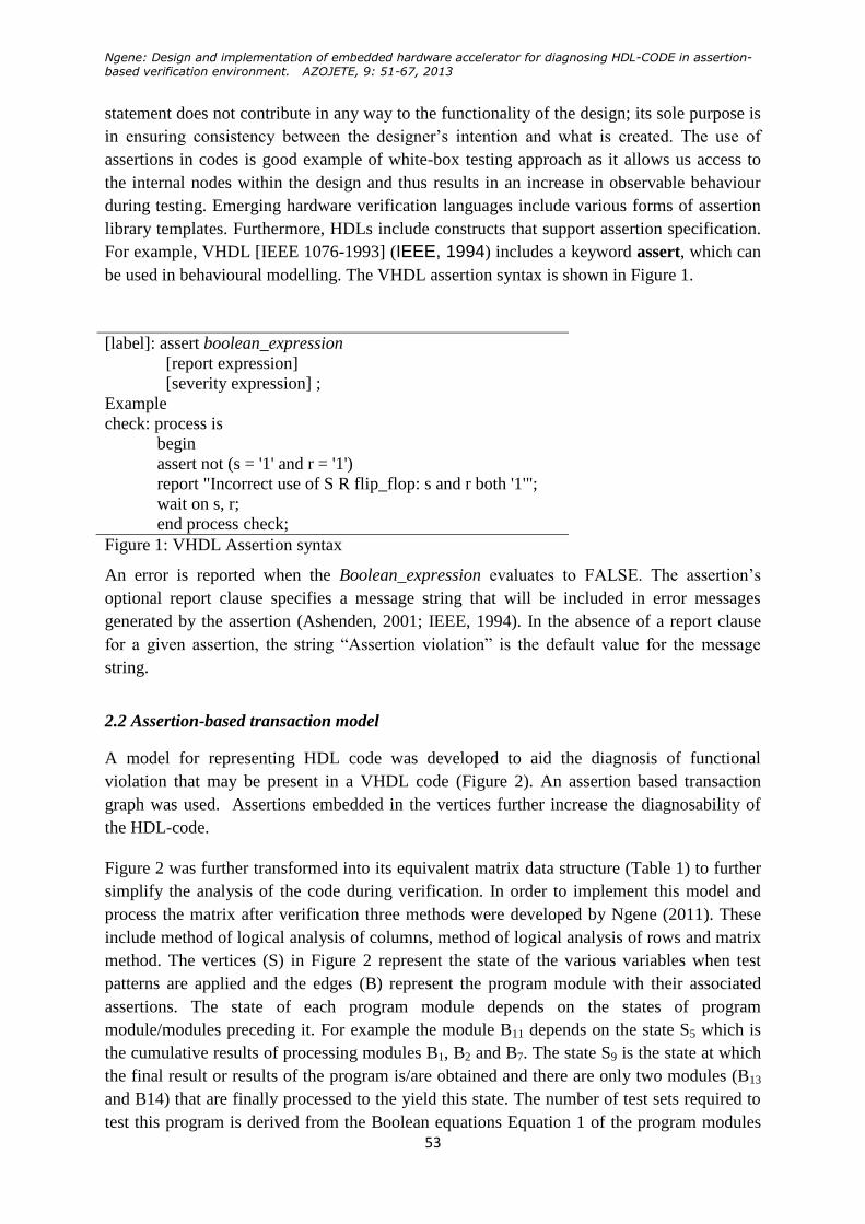
For example, VHDL [IEEE 1076-1993] (IEEE, 1994) includes a keyword assert, which can
be used in behavioural modelling. The VHDL assertion syntax is shown in Figure 1.
[label]: assert boolean_expression
[report expression]
[severity expression] ;
Example
check: process is
begin
assert not (s = '1' and r = '1')
report "Incorrect use of S R flip_flop: s and r both '1'";
wait on s, r;
end process check;
Figure 1: VHDL Assertion syntax
An error is reported when the Boolean_expression evaluates to FALSE. The assertion’s
optional report clause specifies a message string that will be included in error messages
generated by the assertion (Ashenden, 2001; IEEE, 1994). In the absence of a report clause
for a given assertion, the string ―Assertion violation‖ is the default value for the message
string.
2.2 Assertion-based transaction model
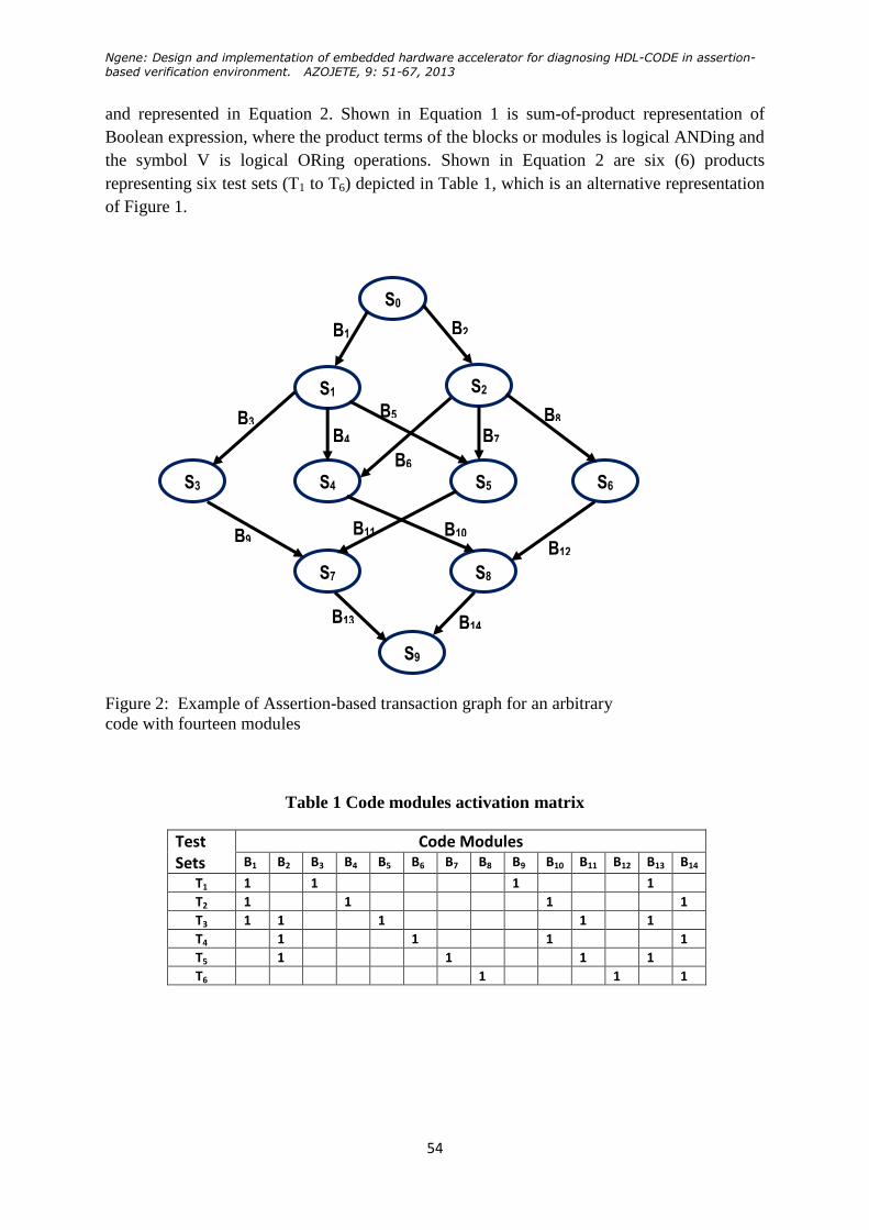
A model for representing HDL code was developed to aid the diagnosis of functional
violation that may be present in a VHDL code (Figure 2). An assertion based transaction
graph was used. Assertions embedded in the vertices further increase the diagnosability of
the HDL-code.
Figure 2 was further transformed into its equivalent matrix data structure (Table 1) to further
simplify the analysis of the code during verification. In order to implement this model and
process the matrix after verification three methods were developed by Ngene (2011). These
include method of logical analysis of columns, method of logical analysis of rows and matrix
method. The vertices (S) in Figure 2 represent the state of the various variables when test
patterns are applied and the edges (B) represent the program module with their associated
assertions. The state of each program module depends on the states of program
module/modules preceding it. For example the module B11 depends on the state S5 which is
the cumulative results of processing modules B1, B2 and B7. The state S9 is the state at which
the final result or results of the program is/are obtained and there are only two modules (B13
and B14) that are finally processed to the yield this state. The number of test sets required to
test this program is derived from the Boolean equations Equation 1 of the program modules
Ngene: Design and implementation of embedded hardware accelerator for diagnosing HDL-CODE in assertion-based verification environment. AZOJETE, 9: 51-67, 2013
54
and represented in Equation 2. Shown in Equation 1 is sum-of-product representation of
Boolean expression, where the product terms of the blocks or modules is logical ANDing and
the symbol V is logical ORing operations. Shown in Equation 2 are six (6) products
representing six test sets (T1 to T6) depicted in Table 1, which is an alternative representation
of Figure 1.
Figure 2: Example of Assertion-based transaction graph for an arbitrary
code with fourteen modules
Table 1 Code modules activation matrix
Test Sets
Code Modules B1 B2 B3 B4 B5 B6 B7 B8 B9 B10 B11 B12 B13 B14
T1 1 1 1 1
T2 1 1 1 1
T3 1 1 1 1 1
T4 1 1 1 1
T5 1 1 1 1
T6 1 1 1
B4
B14
5
B5
B6
B3
B9 B11 B10
B13
B12
B2
B8
B7
B1
S0
S2
S1
S3
S4
S5
S6
S7
S8
S9
Ngene: Design and implementation of embedded hardware accelerator for diagnosing HDL-CODE in assertion-based verification environment. AZOJETE, 9: 51-67, 2013
55
(1)
)2(.SSSSSSSSSSSSSSSSSSSSSSSSSSSSSST 986209752098420975109841097310
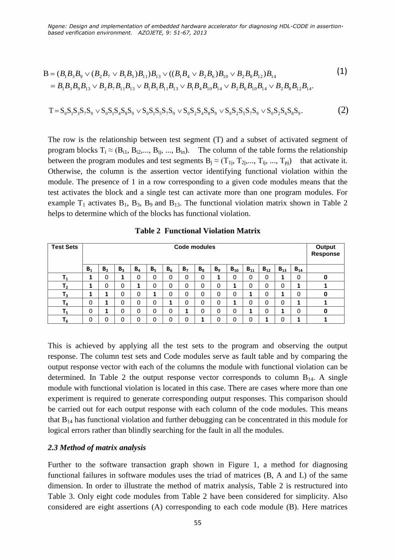
The row is the relationship between test segment (T) and a subset of activated segment of
program blocks Ti ≈ (Bi1, Bi2,..., Bij, ..., Bin). The column of the table forms the relationship
between the program modules and test segments Bj ≈ (T1j, T2j,..., Tij, ..., Tpj) that activate it.
Otherwise, the column is the assertion vector identifying functional violation within the
module. The presence of 1 in a row corresponding to a given code modules means that the
test activates the block and a single test can activate more than one program modules. For
example T1 activates B1, B3, B9 and B13. The functional violation matrix shown in Table 2
helps to determine which of the blocks has functional violation.
Table 2 Functional Violation Matrix
Test Sets Code modules Output Response
B1 B2 B3 B4 B5 B6 B7 B8 B9 B10 B11 B12 B13 B14
T1 1 0 1 0 0 0 0 0 1 0 0 0 1 0 0
T2 1 0 0 1 0 0 0 0 0 1 0 0 0 1 1
T3 1 1 0 0 1 0 0 0 0 0 1 0 1 0 0
T4 0 1 0 0 0 1 0 0 0 1 0 0 0 1 1
T5 0 1 0 0 0 0 1 0 0 0 1 0 1 0 0
T6 0 0 0 0 0 0 0 1 0 0 0 1 0 1 1
This is achieved by applying all the test sets to the program and observing the output
response. The column test sets and Code modules serve as fault table and by comparing the
output response vector with each of the columns the module with functional violation can be
determined. In Table 2 the output response vector corresponds to column B14. A single
module with functional violation is located in this case. There are cases where more than one
experiment is required to generate corresponding output responses. This comparison should
be carried out for each output response with each column of the code modules. This means
that B14 has functional violation and further debugging can be concentrated in this module for
logical errors rather than blindly searching for the fault in all the modules.
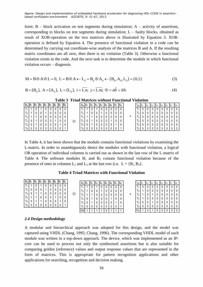
2.3 Method of matrix analysis
Further to the software transaction graph shown in Figure 1, a method for diagnosing
functional failures in software modules uses the triad of matrices (B, A and L) of the same
dimension. In order to illustrate the method of matrix analysis, Table 2 is restructured into
Table 3. Only eight code modules from Table 2 have been considered for simplicity. Also
considered are eight assertions (A) corresponding to each code module (B). Here matrices
.
))(())((B
14128214106214104113115113117213931
14128210624113115172931
BBBBBBBBBBBBBBBBBBBBBBBB
BBBBBBBBBBBBBBBBBB
Ngene: Design and implementation of embedded hardware accelerator for diagnosing HDL-CODE in assertion-based verification environment. AZOJETE, 9: 51-67, 2013
56
form: B – block activation on test segments during simulation; A – activity of assertions,
corresponding to blocks on test segments during simulation; L – faulty blocks, obtained as
result of XOR-operation on the two matrices above is illustrated by Equation 3. XOR-
operation is defined by Equation 4. The presence of functional violation in a code can be
determined by carrying out coordinate-wise analysis of the matrices B and A. If the resulting
matrix coordinates are all zero, then there is no violation (Table 3). Otherwise a functional
violation exists in the code. And the next task is to determine the module in which functional
violation occurs – diagnosis.
{0,1}}L,A,{BABLABL 0,LABM ijijijijijij (3)
. ;m1,j ;n1,i ],[LL ],[AA ],[BB ijijij baba (4)
Table 3 Triad Matrices without Functional Violation
In Table 4, it has been shown that the module contains functional violations by examining the
L-matrix. In order to unambiguously detect the modules with functional violation, a logical
OR operation of individual columns is carried out as shown in the last row of the L-matrix of
Table 4. The software modules B1 and B3 contain functional violation because of the
presence of ones in columns L1 and L3 at the last row (i.e. L = {B1, B3}.
Table 4 Triad Matrices with Functional Violation
2.4 Design methodology
A modular and hierarchical approach was adopted for this design, and the model was
captured using VHDL (Chang, 1995; Chang, 1996). The corresponding VHDL model of each
module was written in a top-down approach. The device, which was implemented as an IP-
core can be used to process not only the synthesised assertions but is also suitable for
comparing golden (reference) values and output response values that are represented in the
form of matrices. This is appropriate for pattern recognition applications and other
applications for searching, recognition and decision making.
Bijj B1 B2 B3 B4 B5 B6 B7 B8
T1 1 0 1 0 0 0 0 0
T2 1 0 0 1 0 0 0 0
T3 1 1 0 0 0 0 0 0
T4 0 1 0 0 0 1 0 0
T5 0 1 0 0 0 0 1 0
T6 0 0 0 0 0 0 0 1
Aijj A1 A2 A3 A4 A5 A6 A7 A8
T1 1 0 1 0 0 0 0 0
T2 1 0 0 1 0 0 0 0
T3 1 1 0 0 0 0 0 0
T4 0 1 0 0 0 1 0 0
T5 0 1 0 0 0 0 1 0
T6 0 0 0 0 0 0 0 1
Lijj L1 L2 L3 L4 L5 L6 L7 L8
T1 0 0 0 0 0 0 0 0
T2 0 0 0 0 0 0 0 0
T3 0 0 0 0 0 0 0 0
T4 0 0 0 0 0 0 0 0
T5 0 0 0 0 0 0 0 0
T6 0 0 0 0 0 0 0 0
Bijj B1 B2 B3 B4 B5 B6 B7 B8
T1 1 0 1 0 0 0 0 0
T2 0 0 0 1 0 0 0 0
T3 0 1 1 0 0 0 0 0
T4 1 1 0 0 0 1 0 0
T5 0 1 1 0 0 0 1 0
T6 0 0 0 0 0 0 0 1
Aijj A1 A2 A3 A4 A5 A6 A7 A8
T1 1 0 1 0 0 0 0 0
T2 1 0 0 1 0 0 0 0
T3 1 1 0 0 0 0 0 0
T4 0 1 0 0 0 1 0 0
T5 0 1 0 0 0 0 1 0
T6 0 0 0 0 0 0 0 1
VAi 1 1 1 1 0 1 1 1
Lijj L1 L2 L3 L4 L5 L6 L7 L8
T1 0 0 0 0 0 0 0 0
T2 1 0 0 0 0 0 0 0
T3 1 0 1 0 0 0 0 0
T4 1 0 0 0 0 0 0 0
T5 0 0 1 0 0 0 0 0
T6 0 0 0 0 0 0 0 0
VLi 1 0 1 0 0 0 0 0
=
=
Ngene: Design and implementation of embedded hardware accelerator for diagnosing HDL-CODE in assertion-based verification environment. AZOJETE, 9: 51-67, 2013
57
2.5 Choice of methods:
The design was based on a tabular data structure with rows containing the test vectors that
activate a subset of the code module (columns) and corresponding output response vector
(Figure 2 and Table 1). The matrix method discussed in the previous section was used to
accomplish the design because it provides the right relationship between the test vectors, code
modules, assertions and functional violations and can achieve the same results as the other
two methods discussed in Ngene (2011). With the achievement of the desired diagnostic
resolution using the proposed methods, logic synthesis scheme and functional coverage
analysis and test generation were used to create software and hardware infrastructure for the
diagnosis of HDL- code.
2.6 Choice of HDL and EDA tool
As earlier mentioned there are two popular HDLs available (VHDL and Verilog) to use for
this design, but VHDL was used in view of its strength in paper documentation. The EDA
tool used for the VHDL code was Xilinx ISE 13 design suite web edition. The design was
partitioned into 2 – the top module and the execution unit. The execution unit in turn consists
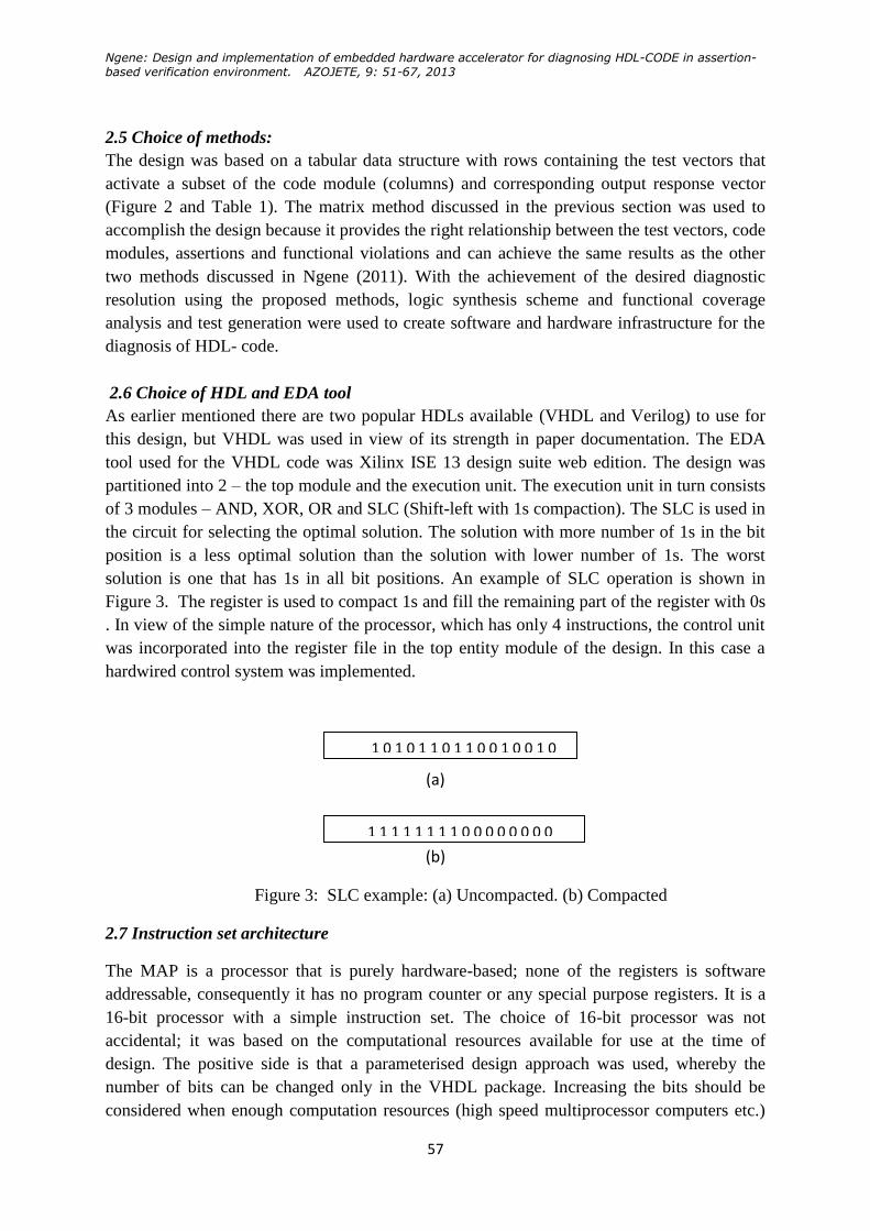
of 3 modules – AND, XOR, OR and SLC (Shift-left with 1s compaction). The SLC is used in
the circuit for selecting the optimal solution. The solution with more number of 1s in the bit
position is a less optimal solution than the solution with lower number of 1s. The worst
solution is one that has 1s in all bit positions. An example of SLC operation is shown in
Figure 3. The register is used to compact 1s and fill the remaining part of the register with 0s
. In view of the simple nature of the processor, which has only 4 instructions, the control unit
was incorporated into the register file in the top entity module of the design. In this case a
hardwired control system was implemented.
(a)
(b)
Figure 3: SLC example: (a) Uncompacted. (b) Compacted
2.7 Instruction set architecture
The MAP is a processor that is purely hardware-based; none of the registers is software
addressable, consequently it has no program counter or any special purpose registers. It is a
16-bit processor with a simple instruction set. The choice of 16-bit processor was not
accidental; it was based on the computational resources available for use at the time of
design. The positive side is that a parameterised design approach was used, whereby the
number of bits can be changed only in the VHDL package. Increasing the bits should be
considered when enough computation resources (high speed multiprocessor computers etc.)
1 0 1 0 1 1 0 1 1 0 0 1 0 0 1 0
0 R0
1 1 1 1 1 1 1 1 0 0 0 0 0 0 0 0
Ngene: Design and implementation of embedded hardware accelerator for diagnosing HDL-CODE in assertion-based verification environment. AZOJETE, 9: 51-67, 2013
58
that could speed up the synthesis to a few days depending on the size of the code are
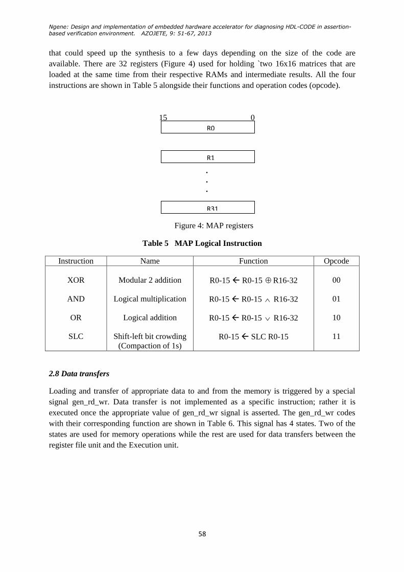
available. There are 32 registers (Figure 4) used for holding `two 16x16 matrices that are
loaded at the same time from their respective RAMs and intermediate results. All the four
instructions are shown in Table 5 alongside their functions and operation codes (opcode).
15 0
.
.
.
Figure 4: MAP registers
Table 5 MAP Logical Instruction
Instruction Name Function Opcode
XOR
AND
OR
SLC
Modular 2 addition
Logical multiplication
Logical addition
Shift-left bit crowding
(Compaction of 1s)
R0-15 R0-15 R16-32
R0-15 R0-15 R16-32
R0-15 R0-15 R16-32
R0-15 SLC R0-15
00
01
10
11
2.8 Data transfers
Loading and transfer of appropriate data to and from the memory is triggered by a special
signal gen_rd_wr. Data transfer is not implemented as a specific instruction; rather it is
executed once the appropriate value of gen_rd_wr signal is asserted. The gen_rd_wr codes
with their corresponding function are shown in Table 6. This signal has 4 states. Two of the
states are used for memory operations while the rest are used for data transfers between the
register file unit and the Execution unit.
R0
R1
R31
Ngene: Design and implementation of embedded hardware accelerator for diagnosing HDL-CODE in assertion-based verification environment. AZOJETE, 9: 51-67, 2013
59
Table 6 Data Transfer Function and their Codes
Transfer Function Opcode Gen_rd_wr
From RAM
To Exec_unit
From Exec_unit
To RAM
R0-15 (RAM1)
Exec (R0-15)
R0-15 (Exec)
RAM4 (R0-15)
any
any
any
any
001
010
011
100
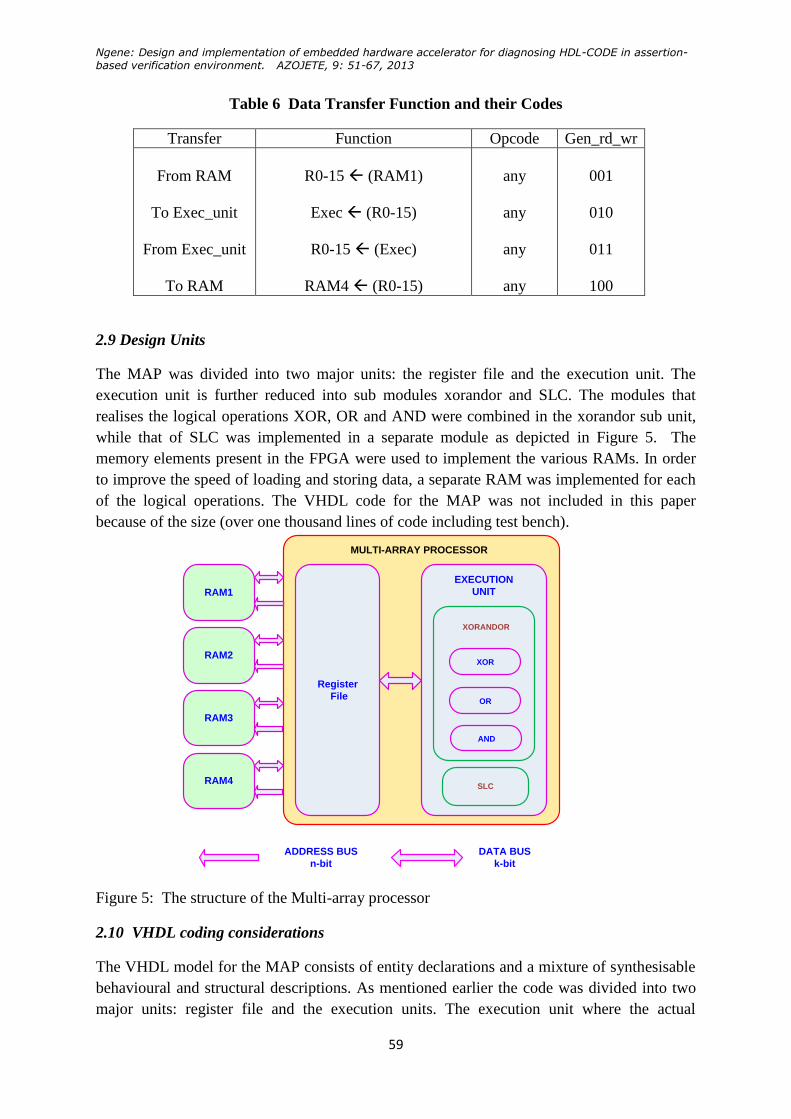
2.9 Design Units
The MAP was divided into two major units: the register file and the execution unit. The
execution unit is further reduced into sub modules xorandor and SLC. The modules that
realises the logical operations XOR, OR and AND were combined in the xorandor sub unit,
while that of SLC was implemented in a separate module as depicted in Figure 5. The
memory elements present in the FPGA were used to implement the various RAMs. In order
to improve the speed of loading and storing data, a separate RAM was implemented for each
of the logical operations. The VHDL code for the MAP was not included in this paper
because of the size (over one thousand lines of code including test bench).
ADDRESS BUS
n-bit
DATA BUS
k-bit
MULTI-ARRAY PROCESSOR
RAM1
RAM4
RAM3
RAM2
Register
File
EXECUTION
UNIT
SLC
XORANDOR
XOR
OR
AND
Figure 5: The structure of the Multi-array processor
2.10 VHDL coding considerations
The VHDL model for the MAP consists of entity declarations and a mixture of synthesisable
behavioural and structural descriptions. As mentioned earlier the code was divided into two
major units: register file and the execution units. The execution unit where the actual
Ngene: Design and implementation of embedded hardware accelerator for diagnosing HDL-CODE in assertion-based verification environment. AZOJETE, 9: 51-67, 2013
60
computation takes place was further divided into sub units; one of the sub units does the
XOR, AND and OR computation and the second sub unit executes the SLC operations. The
sub units were instantiated as components in the execution unit and the execution unit was
further instantiated as a component in the top module entity –register file. However, before
the units were written the types used in the external and internal interfaces in a package called
map_type_pkg were defined. In order to ensure future enhancements of the code, the code
was parameterised to allow for the register and the bus widths to be increased only in one
place (i.e. in the MAP type’s package).
4. Results and discussion
The results of the actual design of the multi-array processor are first presented by examining
the synthesis and the simulation results. Then, the overall improvement brought about by the
use of the device in an assertion-based integrated verification environment for HDL models
of SoCs was highlighted.
4.1 Synthesis
The processor was synthesised with Xilinx ISE 13.1 design suite and simulated using Xilinx
ISIM. Test benches were used to verify the functionality of the design, which was
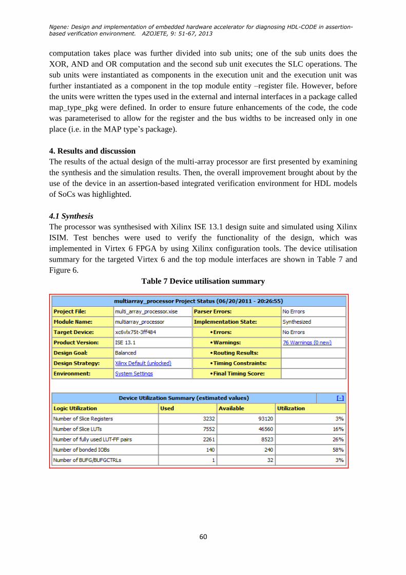
implemented in Virtex 6 FPGA by using Xilinx configuration tools. The device utilisation
summary for the targeted Virtex 6 and the top module interfaces are shown in Table 7 and
Figure 6.
Table 7 Device utilisation summary
Ngene: Design and implementation of embedded hardware accelerator for diagnosing HDL-CODE in assertion-based verification environment. AZOJETE, 9: 51-67, 2013
61
Figure 6: Interfaces of MAP
It is evident from the summary that some parts of the device were poorly utilised, especially
the number of slice registers and BUFG/BUFGCTRLs. The reason for choosing Virtex 6 was
because there was a large number of the bonded input/output blocks whose utilisation was
above 50%. The input/output lines were large due to the high level of parallelism of the
design, which generally improved the speed of operation of the device at the expense of area
or large number of primitives used. The components interconnection implementation is
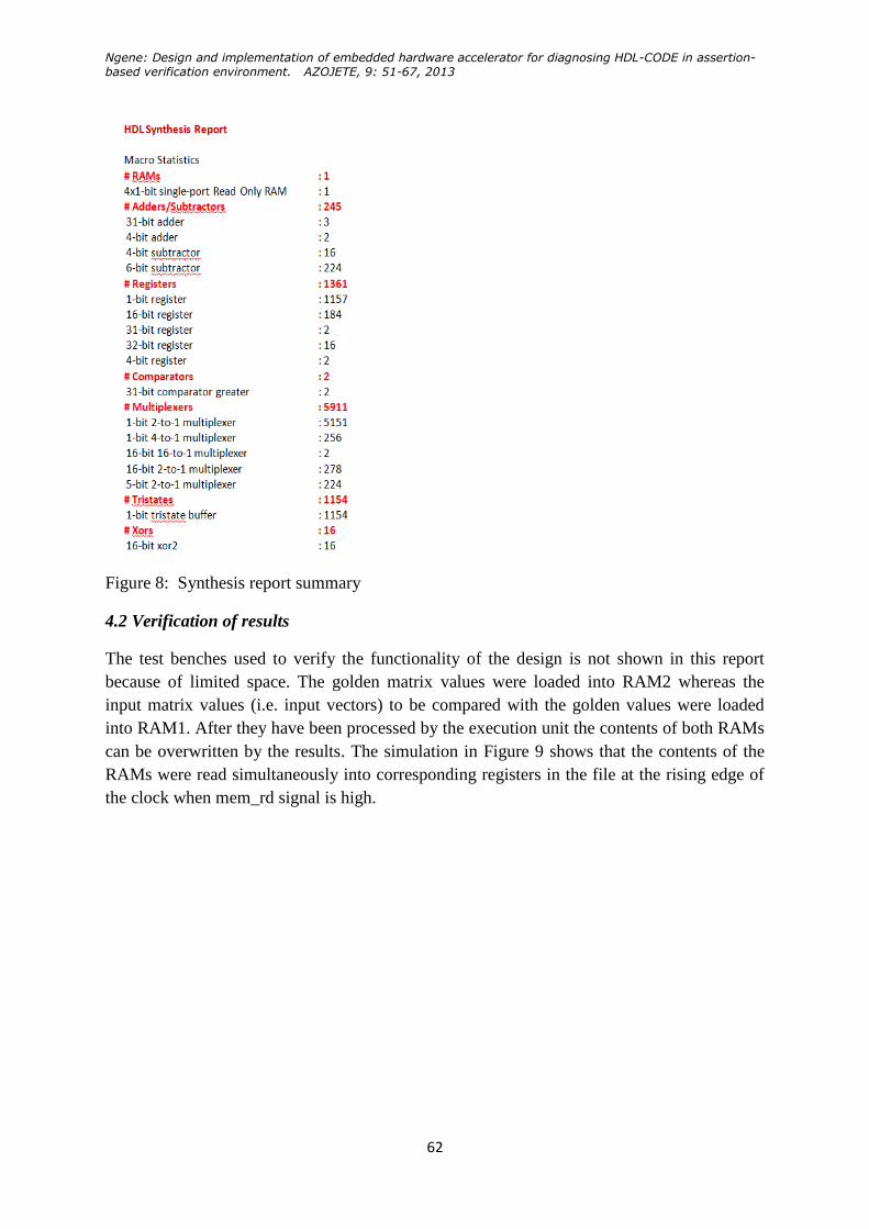
shown in Figure 7. The synthesis report showing various components used and their total
number is shown in Figure 8 rather than the actual netlist (logic components and their
interconnection).
Figure 7: Components interconnection implementation
Ngene: Design and implementation of embedded hardware accelerator for diagnosing HDL-CODE in assertion-based verification environment. AZOJETE, 9: 51-67, 2013
62
Figure 8: Synthesis report summary
4.2 Verification of results
The test benches used to verify the functionality of the design is not shown in this report
because of limited space. The golden matrix values were loaded into RAM2 whereas the
input matrix values (i.e. input vectors) to be compared with the golden values were loaded
into RAM1. After they have been processed by the execution unit the contents of both RAMs
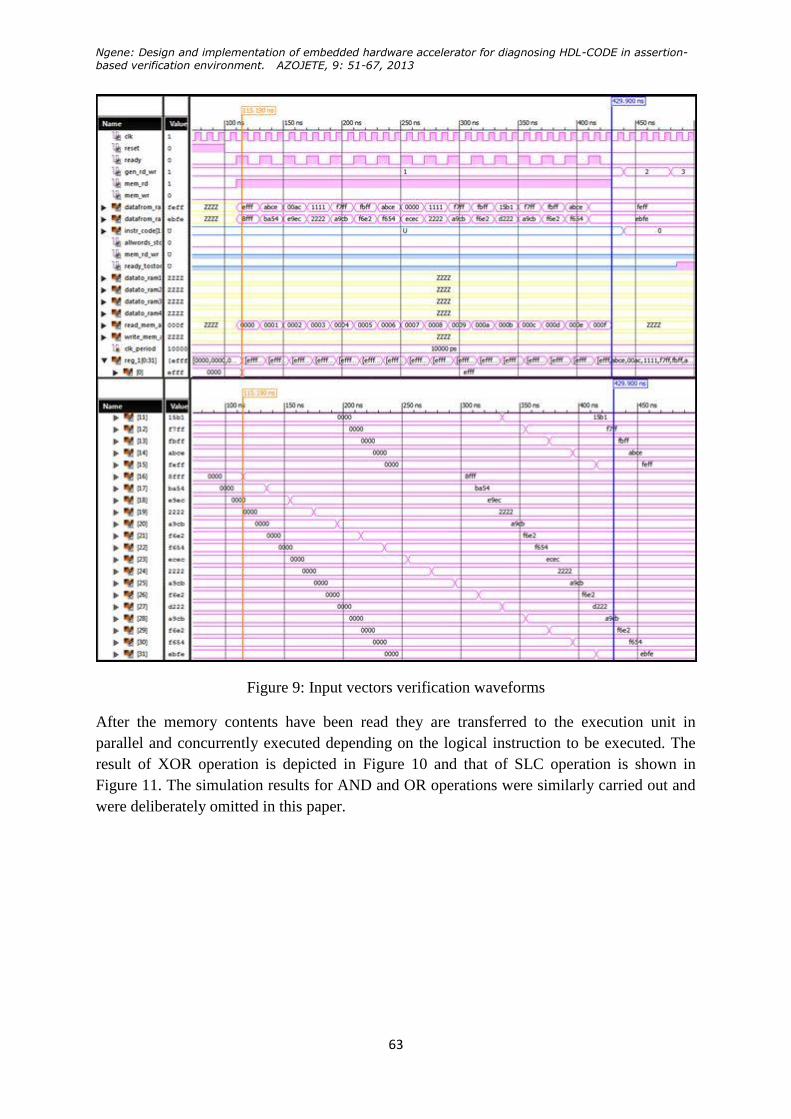
can be overwritten by the results. The simulation in Figure 9 shows that the contents of the
RAMs were read simultaneously into corresponding registers in the file at the rising edge of
the clock when mem_rd signal is high.
Ngene: Design and implementation of embedded hardware accelerator for diagnosing HDL-CODE in assertion-based verification environment. AZOJETE, 9: 51-67, 2013
63
Figure 9: Input vectors verification waveforms
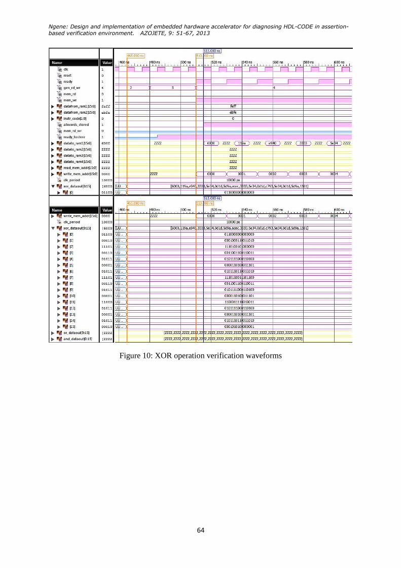
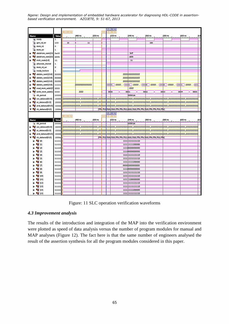
After the memory contents have been read they are transferred to the execution unit in
parallel and concurrently executed depending on the logical instruction to be executed. The
result of XOR operation is depicted in Figure 10 and that of SLC operation is shown in
Figure 11. The simulation results for AND and OR operations were similarly carried out and
were deliberately omitted in this paper.
Ngene: Design and implementation of embedded hardware accelerator for diagnosing HDL-CODE in assertion-based verification environment. AZOJETE, 9: 51-67, 2013
64
Figure 10: XOR operation verification waveforms
Ngene: Design and implementation of embedded hardware accelerator for diagnosing HDL-CODE in assertion-based verification environment. AZOJETE, 9: 51-67, 2013
65
Figure: 11 SLC operation verification waveforms
4.3 Improvement analysis
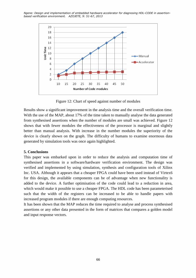
The results of the introduction and integration of the MAP into the verification environment
were plotted as speed of data analysis versus the number of program modules for manual and
MAP analyses (Figure 12). The fact here is that the same number of engineers analysed the
result of the assertion synthesis for all the program modules considered in this paper.
Ngene: Design and implementation of embedded hardware accelerator for diagnosing HDL-CODE in assertion-based verification environment. AZOJETE, 9: 51-67, 2013
66
Figure 12: Chart of speed against number of modules
Results show a significant improvement in the analysis time and the overall verification time.
With the use of the MAP, about 17% of the time taken to manually analyse the data generated
from synthesised assertions when the number of modules are small was achieved. Figure 12
shows that with fewer modules the effectiveness of the processor is marginal and slightly
better than manual analysis. With increase in the number modules the superiority of the
device is clearly shown on the graph. The difficulty of humans to examine enormous data
generated by simulation tools was once again highlighted.
5. Conclusions
This paper was embarked upon in order to reduce the analysis and computation time of
synthesised assertions in a software/hardware verification environment. The design was
verified and implemented by using simulation, synthesis and configuration tools of Xilinx
Inc. USA. Although it appears that a cheaper FPGA could have been used instead of Virtex6
for this design, the available components can be of advantage when new functionality is
added to the device. A further optimisation of the code could lead to a reduction in area,
which would make it possible to use a cheaper FPGA. The HDL code has been parameterised
such that the width of the registers can be increased to be able to handle papers with
increased program modules if there are enough computing resources.
It has been shown that the MAP reduces the time required to analyse and process synthesised
assertions or any other data presented in the form of matrices that compares a golden model
and input response vectors.
Ngene: Design and implementation of embedded hardware accelerator for diagnosing HDL-CODE in assertion-based verification environment. AZOJETE, 9: 51-67, 2013
67
References
Andrew, A., O’Fallon, A. and Chen T. 2003. A Rule-Based Software Testing Method
forVHDL Models Proceedings. IFIPInternational Conf. of VLSI SoC, Darmstadt, Germany.
Ashenden, PJ. 2001. The Designer’s Guide to VHDL, 2nd
ed. Morgan Kaufmann Publishers,
San Francisco. pp138 – 140.
Bergeron, J. 2003. Writing Test Benches: Functional Verification of HDL Models, 2nd
ed.,
Kluwer Academic Publishers. Boston, USA.
Chang, M. 1995. From VHDL to CPLD — a Synthesizable Journey, One-day Tutorial
Workshop, IEEE International ASIC Conference, Austin, Texas.
Chang, M. 1996. Teaching Top-down Design Using VHDL and CPLD. Proceedings of
Frontiers in Education Conference, 2: 514 – 517.
Foster, HD., Krolnik, AC. and Lacey, DJ. 2004. Assertion-Based Design, 2nd
ed. Kluwer
Academic Publishers, Boston, USA.
IEEE. 1994. IEEE Standard VHDL Language Reference Manual: ANSI/IEEE Standard
1076–1993. New York.
Kalyaev, IA., Levin, II., Semernikov, EA. 2011. Reconfigurable System Uses Large FPGA
Computation Fields. Xcell Journal, 75: 24 – 29.
Ngene, CU. 2011. Embedded Diagnostic Infrastructure for HDL-models of Digital Systems
on Chip, Ph.D Dissertation, Kharkov National University of Radioelectronics.
Seward, SR. and Lala, PK. 2003. Fault Injection for Verifying Testability at the VHDL
Level. IEEE ITC International Test Conference, pp 131 – 137.
Xilinx. 2011. ISE In-Depth Tutorial. UG695 (v13.1). www.xilinx.com
Xilinx. 2010. XST User Guide for Virtex-6 and Spartan-6 Devices. UG687 (v 12.1)
www.xilinx.com