Embed Size (px)
Citation preview
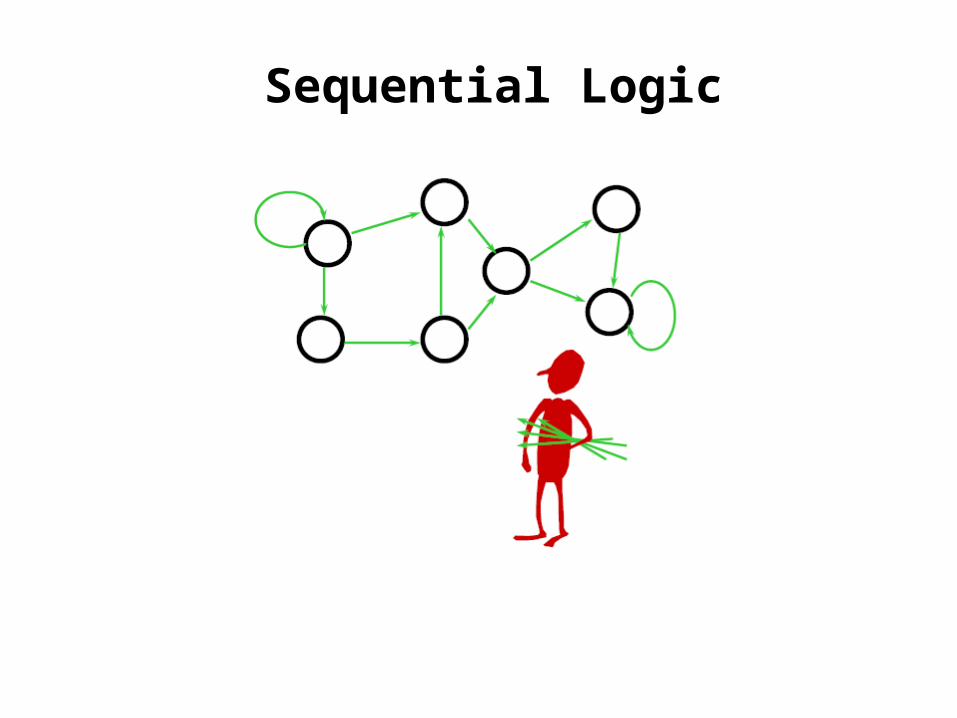
Sequential Logic
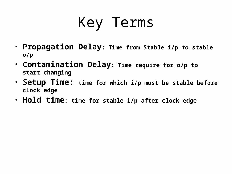
Key Terms
bull Propagation Delay Time from Stable ip to stable op
bull Contamination Delay Time require for op to start changing
bull Setup Time time for which ip must be stable before clock edge
bull Hold time time for stable ip after clock edge
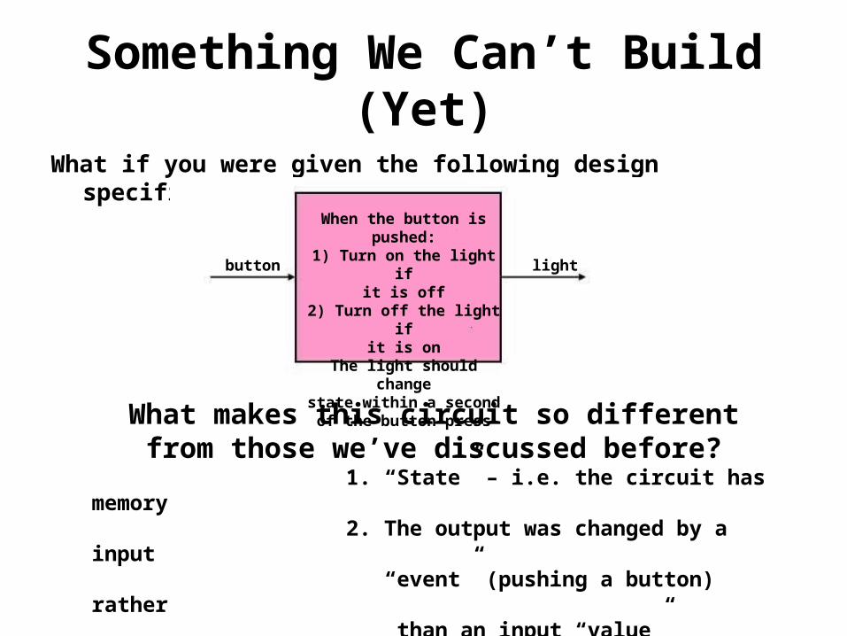
Something We Canrsquot Build (Yet)
What if you were given the following design specification
When the button is pushed1) Turn on the light if
it is off2) Turn off the light if
it is onThe light should change
state within a secondof the button press
What makes this circuit so differentfrom those wersquove discussed before
1 ldquoStaterdquo ndash ie the circuit has memory 2 The output was changed by a input ldquoeventrdquo (pushing a button) rather than an input ldquovaluerdquo
button light
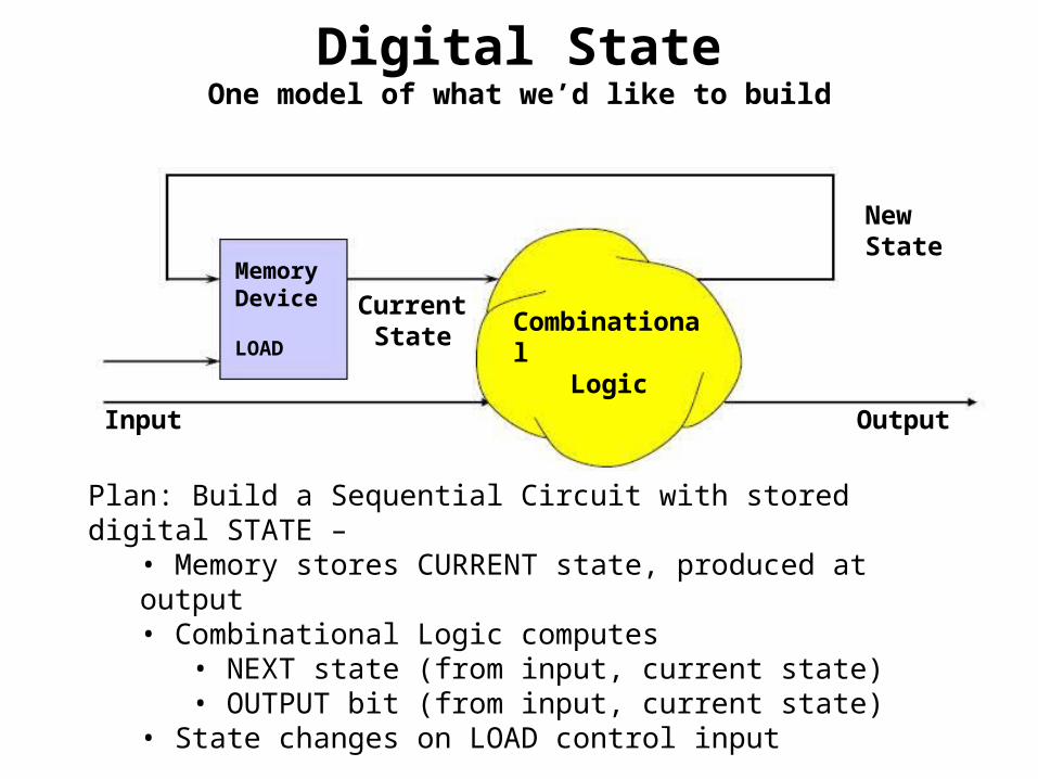
Digital StateOne model of what wersquod like to build
MemoryDevice
LOADCombinational
Logic
NewState
Output
CurrentState
Input
Plan Build a Sequential Circuit with stored digital STATE ndashbull Memory stores CURRENT state produced at outputbull Combinational Logic computes
bull NEXT state (from input current state)bull OUTPUT bit (from input current state)
bull State changes on LOAD control input
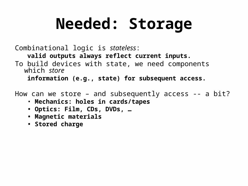
Needed Storage
Combinational logic is statelessvalid outputs always reflect current inputs
To build devices with state we need components which storeinformation (eg state) for subsequent access
How can we store ndash and subsequently access -- a bitbull Mechanics holes in cardstapesbull Optics Film CDs DVDs hellipbull Magnetic materialsbull Stored charge
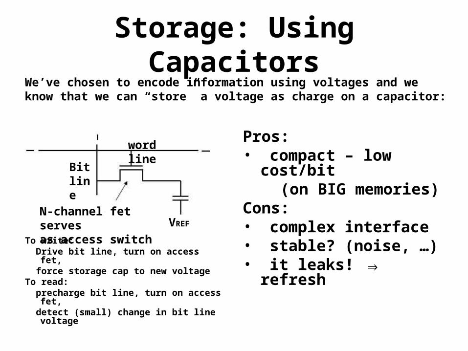
Storage Using Capacitors
To write Drive bit line turn on access fet force storage cap to new voltageTo read precharge bit line turn on access fet detect (small) change in bit line
voltage
Prosbull compact ndash low costbit (on BIG memories)Consbull complex interfacebull stable (noise hellip)bull it leaks rArr refresh
Wersquove chosen to encode information using voltages and we know that we can ldquostorerdquo a voltage as charge on a capacitor
Bitline
N-channel fet servesas access switch VREF
word line
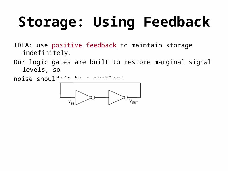
Storage Using Feedback
IDEA use positive feedback to maintain storage indefinitely
Our logic gates are built to restore marginal signal levels so
noise shouldnrsquot be a problem
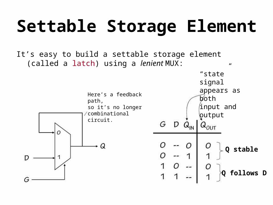
Settable Storage Element
Itrsquos easy to build a settable storage element (called a latch) using a lenient MUX
Herersquos a feedback pathso itrsquos no longer acombinational circuit
ldquostaterdquo signalappears as bothinput and output
Q stable
Q follows D
New Device D Latch
G=1Q follows D
G=0Q holds
BUThellip A change in D or Gcontaminates Q hence Qrsquohellip how can this possibly
workG=1 Q Follows D independently of QrsquoG=0 Q Holds stable Qrsquo independentlyof D
A Plea for Leniencehellip
Assume LENIENT Mux propagationdelay of TPDThen output valid when
bull Qrsquo=D stable for TPD independently of G orbull G=1 D stable for TPD independently of Qrsquoorbull G=0 Qrsquo stable for TPD independently of D
hellip with a little disciplineD stable
To reliably latch V2bull Apply V2 to D holding G=1bull After another TPD Qrsquo amp D both valid for TPD will hold Q=V2 independently of Gbull Set G=0 while Qrsquo amp D hold Q=Dbull After TPD V2 appears at Q=Qrsquobull After another TPDG=0 and Qrsquo are sufficient to hold Q=V2 independently of D
Dynamic Discipline for our latchTSETUP = 2TPD interval prior to Gtransition for which D must bestable amp validTHOLD = TPD interval following Gtransition for which D must bestable amp valid
Lets try it out
Plan Build a Sequential Circuit with one bit of STATE ndash
bull Single latch holds CURRENT statebull Combinational Logic computes
bull NEXT state (from input current state)bull OUTPUT bit (from input current state)
bull State changes when G = 1 (briefly)
What happenswhen G=1
Input Output
CombinationalLogic
CurrentState
NewState
Combinational Cycles
CombinationalLogic
CurrentState
NewState
OutputInput
When G=1 latch is Transparenthelliphellip provides a combinational path from D to Q
Canrsquot work without tricky timing constrants on G=1 pulse
bull Must fit within contamination delay of logicbull Must accommodate latch setup hold times
Want to signal an INSTANT not an INTERVALhellip
Analogy
Analogy (cont)
Analogy (cont)
Analogy (cont)
The SolutionAdd two gatesand only openone at a time
Analogy (cont)
The SolutionAdd two gatesand only openone at a time
Analogy (cont)
The SolutionAdd two gatesand only openone at a time
Analogy (cont)
The SolutionAdd two gatesand only openone at a time
Analogy (cont)
The SolutionAdd two gatesand only openone at a time
Analogy (cont)
The SolutionAdd two gatesand only openone at a time
Analogy (cont)
The SolutionAdd two gatesand only openone at a time
Analogy (cont)
The SolutionAdd two gatesand only openone at a time
Edge-triggered Flip FlopThe gate of thislatch is open whenthe clock is low
The gate of thislatch is open whenthe clock is high
master slave
Observationsbull 1048714 only one latch ldquotransparentrdquo at any time
bull 1048714 master closed when slave is openbull 1048714 slave closed when master is openrarr no combinational path through flip flop
bull 1048714 Q only changes shortly after 0 rarr1transition of CLK so flip flop appearsto be ldquotriggeredrdquo by rising edge of CLK
Transitions markinstants not intervals
Flip Flop Waveforms
master slave
CLK
master closedslave open
slave closedmaster open
Um about that hold timehellip
master slave
The masterrsquos contaminationdelay must meet the holdtime of the slave
Consider HOLD TIME requirement for slavebull Negative (1 rarr0) clock transition rarr slave freezes data
bull SHOULD be no output glitch since master held constant data BUTbull master output contaminated by change in G input
bull HOLD TIME of slave not met UNLESS we assume sufficientcontamination delay in the path to its D input
Accumulated tCD thru inverter G rarr Q path of master must coverslave tHOLD for this design to work
Flip Flop Timing - I
tPD maximum propagation delay CLK rarrQtCD minimum contamination delay CLK rarrQ
tSETUP setup timeguarantee that D has propagated through feedback path before master closes
tHOLD hold timeguarantee master is closed and data is stable before allowing D to change
Single-clock Synchronous Circuits
Does thatsymbolregister
Wersquoll use Flip Flops and Registers ndash groups of FFs sharing a clockinput ndash in a highly constrained way to build digitial systems
Single-clock Synchronous Discipline
bull Only care about value of combinationalcircuits just before rising edge ofclock
bull Single clock signal shared amongall clocked devices
bull Period greater than everycombinational delay
Model Discrete TimeNewState
CurrentState
Clock
Input Output
CombinationalLogic
Questionsbull Constraints on TCD for the logic
bull Minimum clock period
bull Setup Hold times for Inputs
SummaryldquoSequentialrdquo Circuits (with memory)
Basic memory elementsbull Feedback detailed analysis =gt basic level-sensitive devices (eg latch)bull 2 Latches =gt Flopbull Dynamic Discipline constraints on input timing
Synchronous 1-clock logicbull Simple rules for sequential circuitsbull Yields clocked circuit with TS TH
constraints on input timing
Key Terms
bull Propagation Delay Time from Stable ip to stable op
bull Contamination Delay Time require for op to start changing
bull Setup Time time for which ip must be stable before clock edge
bull Hold time time for stable ip after clock edge
Something We Canrsquot Build (Yet)
What if you were given the following design specification
When the button is pushed1) Turn on the light if
it is off2) Turn off the light if
it is onThe light should change
state within a secondof the button press
What makes this circuit so differentfrom those wersquove discussed before
1 ldquoStaterdquo ndash ie the circuit has memory 2 The output was changed by a input ldquoeventrdquo (pushing a button) rather than an input ldquovaluerdquo
button light
Digital StateOne model of what wersquod like to build
MemoryDevice
LOADCombinational
Logic
NewState
Output
CurrentState
Input
Plan Build a Sequential Circuit with stored digital STATE ndashbull Memory stores CURRENT state produced at outputbull Combinational Logic computes
bull NEXT state (from input current state)bull OUTPUT bit (from input current state)
bull State changes on LOAD control input
Needed Storage
Combinational logic is statelessvalid outputs always reflect current inputs
To build devices with state we need components which storeinformation (eg state) for subsequent access
How can we store ndash and subsequently access -- a bitbull Mechanics holes in cardstapesbull Optics Film CDs DVDs hellipbull Magnetic materialsbull Stored charge
Storage Using Capacitors
To write Drive bit line turn on access fet force storage cap to new voltageTo read precharge bit line turn on access fet detect (small) change in bit line
voltage
Prosbull compact ndash low costbit (on BIG memories)Consbull complex interfacebull stable (noise hellip)bull it leaks rArr refresh
Wersquove chosen to encode information using voltages and we know that we can ldquostorerdquo a voltage as charge on a capacitor
Bitline
N-channel fet servesas access switch VREF
word line
Storage Using Feedback
IDEA use positive feedback to maintain storage indefinitely
Our logic gates are built to restore marginal signal levels so
noise shouldnrsquot be a problem
Settable Storage Element
Itrsquos easy to build a settable storage element (called a latch) using a lenient MUX
Herersquos a feedback pathso itrsquos no longer acombinational circuit
ldquostaterdquo signalappears as bothinput and output
Q stable
Q follows D
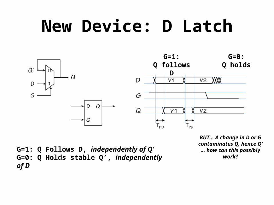
New Device D Latch
G=1Q follows D
G=0Q holds
BUThellip A change in D or Gcontaminates Q hence Qrsquohellip how can this possibly
workG=1 Q Follows D independently of QrsquoG=0 Q Holds stable Qrsquo independentlyof D
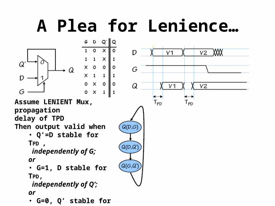
A Plea for Leniencehellip
Assume LENIENT Mux propagationdelay of TPDThen output valid when
bull Qrsquo=D stable for TPD independently of G orbull G=1 D stable for TPD independently of Qrsquoorbull G=0 Qrsquo stable for TPD independently of D
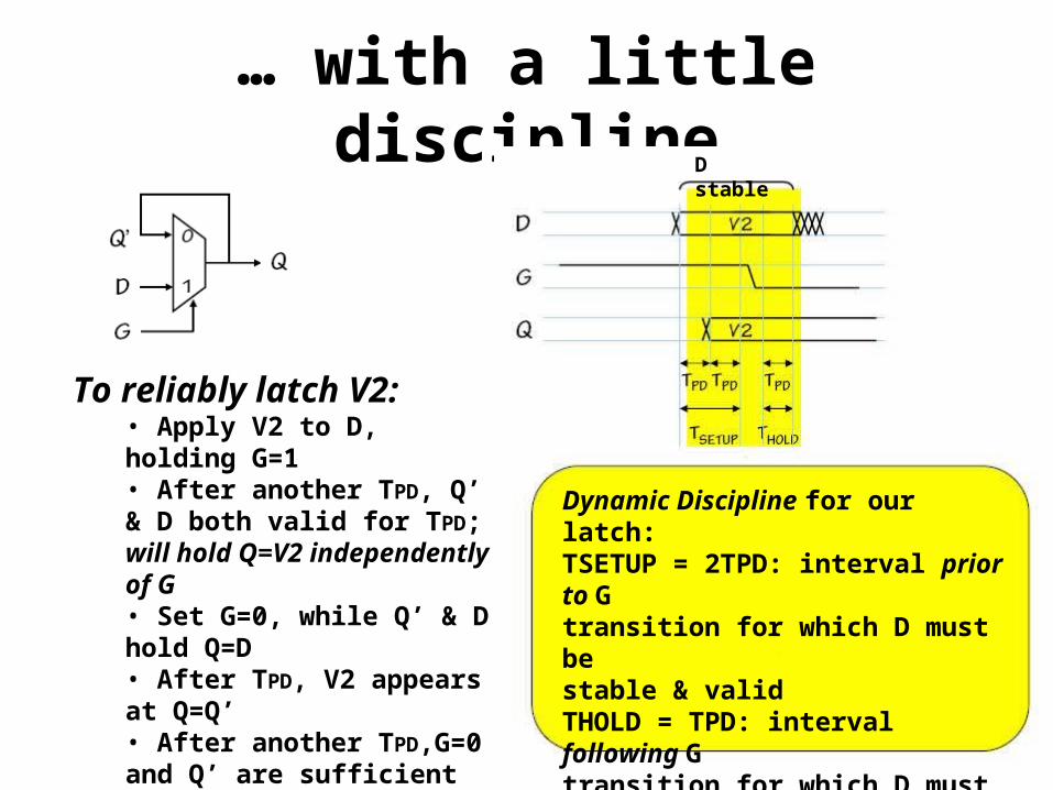
hellip with a little disciplineD stable
To reliably latch V2bull Apply V2 to D holding G=1bull After another TPD Qrsquo amp D both valid for TPD will hold Q=V2 independently of Gbull Set G=0 while Qrsquo amp D hold Q=Dbull After TPD V2 appears at Q=Qrsquobull After another TPDG=0 and Qrsquo are sufficient to hold Q=V2 independently of D
Dynamic Discipline for our latchTSETUP = 2TPD interval prior to Gtransition for which D must bestable amp validTHOLD = TPD interval following Gtransition for which D must bestable amp valid
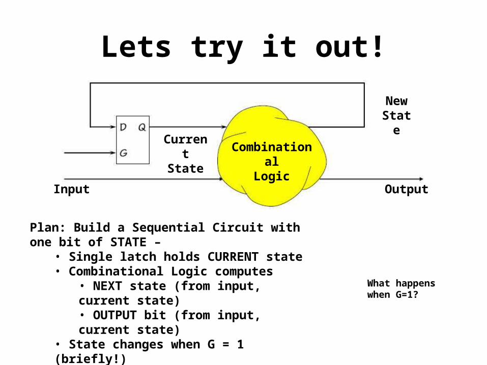
Lets try it out
Plan Build a Sequential Circuit with one bit of STATE ndash
bull Single latch holds CURRENT statebull Combinational Logic computes
bull NEXT state (from input current state)bull OUTPUT bit (from input current state)
bull State changes when G = 1 (briefly)
What happenswhen G=1
Input Output
CombinationalLogic
CurrentState
NewState
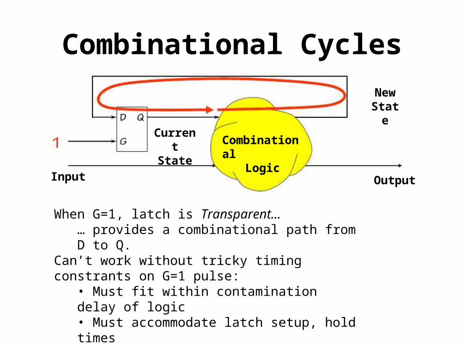
Combinational Cycles
CombinationalLogic
CurrentState
NewState
OutputInput
When G=1 latch is Transparenthelliphellip provides a combinational path from D to Q
Canrsquot work without tricky timing constrants on G=1 pulse
bull Must fit within contamination delay of logicbull Must accommodate latch setup hold times
Want to signal an INSTANT not an INTERVALhellip
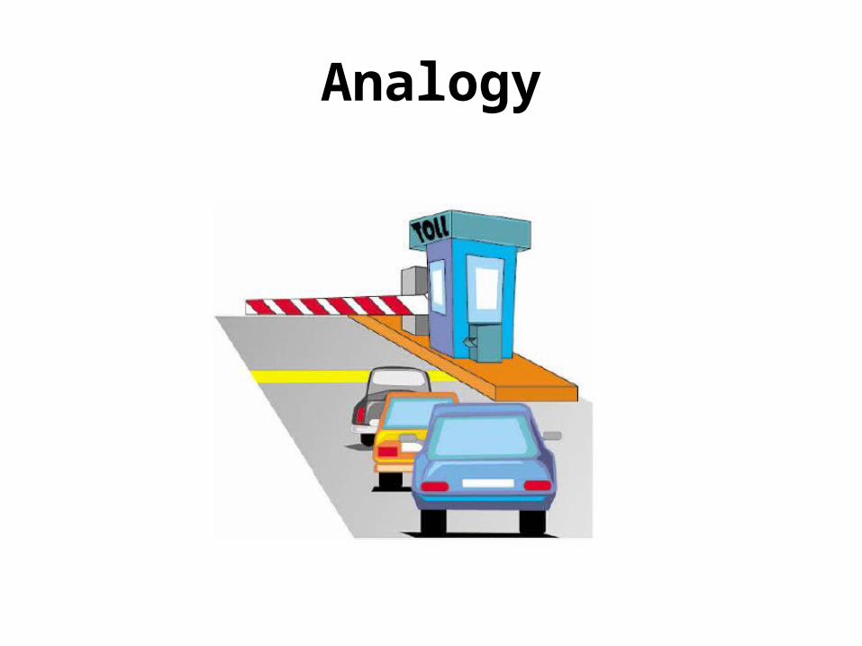
Analogy
Analogy (cont)
Analogy (cont)
Analogy (cont)
The SolutionAdd two gatesand only openone at a time
Analogy (cont)
The SolutionAdd two gatesand only openone at a time
Analogy (cont)
The SolutionAdd two gatesand only openone at a time
Analogy (cont)
The SolutionAdd two gatesand only openone at a time
Analogy (cont)
The SolutionAdd two gatesand only openone at a time
Analogy (cont)
The SolutionAdd two gatesand only openone at a time
Analogy (cont)
The SolutionAdd two gatesand only openone at a time
Analogy (cont)
The SolutionAdd two gatesand only openone at a time
Edge-triggered Flip FlopThe gate of thislatch is open whenthe clock is low
The gate of thislatch is open whenthe clock is high
master slave
Observationsbull 1048714 only one latch ldquotransparentrdquo at any time
bull 1048714 master closed when slave is openbull 1048714 slave closed when master is openrarr no combinational path through flip flop
bull 1048714 Q only changes shortly after 0 rarr1transition of CLK so flip flop appearsto be ldquotriggeredrdquo by rising edge of CLK
Transitions markinstants not intervals
Flip Flop Waveforms
master slave
CLK
master closedslave open
slave closedmaster open
Um about that hold timehellip
master slave
The masterrsquos contaminationdelay must meet the holdtime of the slave
Consider HOLD TIME requirement for slavebull Negative (1 rarr0) clock transition rarr slave freezes data
bull SHOULD be no output glitch since master held constant data BUTbull master output contaminated by change in G input
bull HOLD TIME of slave not met UNLESS we assume sufficientcontamination delay in the path to its D input
Accumulated tCD thru inverter G rarr Q path of master must coverslave tHOLD for this design to work
Flip Flop Timing - I
tPD maximum propagation delay CLK rarrQtCD minimum contamination delay CLK rarrQ
tSETUP setup timeguarantee that D has propagated through feedback path before master closes
tHOLD hold timeguarantee master is closed and data is stable before allowing D to change
Single-clock Synchronous Circuits
Does thatsymbolregister
Wersquoll use Flip Flops and Registers ndash groups of FFs sharing a clockinput ndash in a highly constrained way to build digitial systems
Single-clock Synchronous Discipline
bull Only care about value of combinationalcircuits just before rising edge ofclock
bull Single clock signal shared amongall clocked devices
bull Period greater than everycombinational delay
Model Discrete TimeNewState
CurrentState
Clock
Input Output
CombinationalLogic
Questionsbull Constraints on TCD for the logic
bull Minimum clock period
bull Setup Hold times for Inputs
SummaryldquoSequentialrdquo Circuits (with memory)
Basic memory elementsbull Feedback detailed analysis =gt basic level-sensitive devices (eg latch)bull 2 Latches =gt Flopbull Dynamic Discipline constraints on input timing
Synchronous 1-clock logicbull Simple rules for sequential circuitsbull Yields clocked circuit with TS TH
constraints on input timing
Something We Canrsquot Build (Yet)
What if you were given the following design specification
When the button is pushed1) Turn on the light if
it is off2) Turn off the light if
it is onThe light should change
state within a secondof the button press
What makes this circuit so differentfrom those wersquove discussed before
1 ldquoStaterdquo ndash ie the circuit has memory 2 The output was changed by a input ldquoeventrdquo (pushing a button) rather than an input ldquovaluerdquo
button light
Digital StateOne model of what wersquod like to build
MemoryDevice
LOADCombinational
Logic
NewState
Output
CurrentState
Input
Plan Build a Sequential Circuit with stored digital STATE ndashbull Memory stores CURRENT state produced at outputbull Combinational Logic computes
bull NEXT state (from input current state)bull OUTPUT bit (from input current state)
bull State changes on LOAD control input
Needed Storage
Combinational logic is statelessvalid outputs always reflect current inputs
To build devices with state we need components which storeinformation (eg state) for subsequent access
How can we store ndash and subsequently access -- a bitbull Mechanics holes in cardstapesbull Optics Film CDs DVDs hellipbull Magnetic materialsbull Stored charge
Storage Using Capacitors
To write Drive bit line turn on access fet force storage cap to new voltageTo read precharge bit line turn on access fet detect (small) change in bit line
voltage
Prosbull compact ndash low costbit (on BIG memories)Consbull complex interfacebull stable (noise hellip)bull it leaks rArr refresh
Wersquove chosen to encode information using voltages and we know that we can ldquostorerdquo a voltage as charge on a capacitor
Bitline
N-channel fet servesas access switch VREF
word line
Storage Using Feedback
IDEA use positive feedback to maintain storage indefinitely
Our logic gates are built to restore marginal signal levels so
noise shouldnrsquot be a problem
Settable Storage Element
Itrsquos easy to build a settable storage element (called a latch) using a lenient MUX
Herersquos a feedback pathso itrsquos no longer acombinational circuit
ldquostaterdquo signalappears as bothinput and output
Q stable
Q follows D
New Device D Latch
G=1Q follows D
G=0Q holds
BUThellip A change in D or Gcontaminates Q hence Qrsquohellip how can this possibly
workG=1 Q Follows D independently of QrsquoG=0 Q Holds stable Qrsquo independentlyof D
A Plea for Leniencehellip
Assume LENIENT Mux propagationdelay of TPDThen output valid when
bull Qrsquo=D stable for TPD independently of G orbull G=1 D stable for TPD independently of Qrsquoorbull G=0 Qrsquo stable for TPD independently of D
hellip with a little disciplineD stable
To reliably latch V2bull Apply V2 to D holding G=1bull After another TPD Qrsquo amp D both valid for TPD will hold Q=V2 independently of Gbull Set G=0 while Qrsquo amp D hold Q=Dbull After TPD V2 appears at Q=Qrsquobull After another TPDG=0 and Qrsquo are sufficient to hold Q=V2 independently of D
Dynamic Discipline for our latchTSETUP = 2TPD interval prior to Gtransition for which D must bestable amp validTHOLD = TPD interval following Gtransition for which D must bestable amp valid
Lets try it out
Plan Build a Sequential Circuit with one bit of STATE ndash
bull Single latch holds CURRENT statebull Combinational Logic computes
bull NEXT state (from input current state)bull OUTPUT bit (from input current state)
bull State changes when G = 1 (briefly)
What happenswhen G=1
Input Output
CombinationalLogic
CurrentState
NewState
Combinational Cycles
CombinationalLogic
CurrentState
NewState
OutputInput
When G=1 latch is Transparenthelliphellip provides a combinational path from D to Q
Canrsquot work without tricky timing constrants on G=1 pulse
bull Must fit within contamination delay of logicbull Must accommodate latch setup hold times
Want to signal an INSTANT not an INTERVALhellip
Analogy
Analogy (cont)
Analogy (cont)
Analogy (cont)
The SolutionAdd two gatesand only openone at a time
Analogy (cont)
The SolutionAdd two gatesand only openone at a time
Analogy (cont)
The SolutionAdd two gatesand only openone at a time
Analogy (cont)
The SolutionAdd two gatesand only openone at a time
Analogy (cont)
The SolutionAdd two gatesand only openone at a time
Analogy (cont)
The SolutionAdd two gatesand only openone at a time
Analogy (cont)
The SolutionAdd two gatesand only openone at a time
Analogy (cont)
The SolutionAdd two gatesand only openone at a time
Edge-triggered Flip FlopThe gate of thislatch is open whenthe clock is low
The gate of thislatch is open whenthe clock is high
master slave
Observationsbull 1048714 only one latch ldquotransparentrdquo at any time
bull 1048714 master closed when slave is openbull 1048714 slave closed when master is openrarr no combinational path through flip flop
bull 1048714 Q only changes shortly after 0 rarr1transition of CLK so flip flop appearsto be ldquotriggeredrdquo by rising edge of CLK
Transitions markinstants not intervals
Flip Flop Waveforms
master slave
CLK
master closedslave open
slave closedmaster open
Um about that hold timehellip
master slave
The masterrsquos contaminationdelay must meet the holdtime of the slave
Consider HOLD TIME requirement for slavebull Negative (1 rarr0) clock transition rarr slave freezes data
bull SHOULD be no output glitch since master held constant data BUTbull master output contaminated by change in G input
bull HOLD TIME of slave not met UNLESS we assume sufficientcontamination delay in the path to its D input
Accumulated tCD thru inverter G rarr Q path of master must coverslave tHOLD for this design to work
Flip Flop Timing - I
tPD maximum propagation delay CLK rarrQtCD minimum contamination delay CLK rarrQ
tSETUP setup timeguarantee that D has propagated through feedback path before master closes
tHOLD hold timeguarantee master is closed and data is stable before allowing D to change
Single-clock Synchronous Circuits
Does thatsymbolregister
Wersquoll use Flip Flops and Registers ndash groups of FFs sharing a clockinput ndash in a highly constrained way to build digitial systems
Single-clock Synchronous Discipline
bull Only care about value of combinationalcircuits just before rising edge ofclock
bull Single clock signal shared amongall clocked devices
bull Period greater than everycombinational delay
Model Discrete TimeNewState
CurrentState
Clock
Input Output
CombinationalLogic
Questionsbull Constraints on TCD for the logic
bull Minimum clock period
bull Setup Hold times for Inputs
SummaryldquoSequentialrdquo Circuits (with memory)
Basic memory elementsbull Feedback detailed analysis =gt basic level-sensitive devices (eg latch)bull 2 Latches =gt Flopbull Dynamic Discipline constraints on input timing
Synchronous 1-clock logicbull Simple rules for sequential circuitsbull Yields clocked circuit with TS TH
constraints on input timing
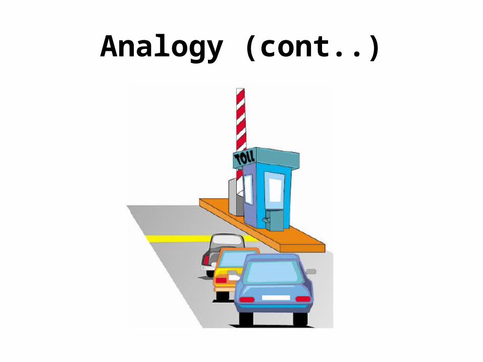
Analogy (cont)
Analogy (cont)
Analogy (cont)
The SolutionAdd two gatesand only openone at a time
Analogy (cont)
The SolutionAdd two gatesand only openone at a time
Analogy (cont)
The SolutionAdd two gatesand only openone at a time
Analogy (cont)
The SolutionAdd two gatesand only openone at a time
Analogy (cont)
The SolutionAdd two gatesand only openone at a time
Analogy (cont)
The SolutionAdd two gatesand only openone at a time
Analogy (cont)
The SolutionAdd two gatesand only openone at a time
Analogy (cont)
The SolutionAdd two gatesand only openone at a time
Edge-triggered Flip FlopThe gate of thislatch is open whenthe clock is low
The gate of thislatch is open whenthe clock is high
master slave
Observationsbull 1048714 only one latch ldquotransparentrdquo at any time
bull 1048714 master closed when slave is openbull 1048714 slave closed when master is openrarr no combinational path through flip flop
bull 1048714 Q only changes shortly after 0 rarr1transition of CLK so flip flop appearsto be ldquotriggeredrdquo by rising edge of CLK
Transitions markinstants not intervals
Flip Flop Waveforms
master slave
CLK
master closedslave open
slave closedmaster open
Um about that hold timehellip
master slave
The masterrsquos contaminationdelay must meet the holdtime of the slave
Consider HOLD TIME requirement for slavebull Negative (1 rarr0) clock transition rarr slave freezes data
bull SHOULD be no output glitch since master held constant data BUTbull master output contaminated by change in G input
bull HOLD TIME of slave not met UNLESS we assume sufficientcontamination delay in the path to its D input
Accumulated tCD thru inverter G rarr Q path of master must coverslave tHOLD for this design to work
Flip Flop Timing - I
tPD maximum propagation delay CLK rarrQtCD minimum contamination delay CLK rarrQ
tSETUP setup timeguarantee that D has propagated through feedback path before master closes
tHOLD hold timeguarantee master is closed and data is stable before allowing D to change
Single-clock Synchronous Circuits
Does thatsymbolregister
Wersquoll use Flip Flops and Registers ndash groups of FFs sharing a clockinput ndash in a highly constrained way to build digitial systems
Single-clock Synchronous Discipline
bull Only care about value of combinationalcircuits just before rising edge ofclock
bull Single clock signal shared amongall clocked devices
bull Period greater than everycombinational delay
Model Discrete TimeNewState
CurrentState
Clock
Input Output
CombinationalLogic
Questionsbull Constraints on TCD for the logic
bull Minimum clock period
bull Setup Hold times for Inputs
SummaryldquoSequentialrdquo Circuits (with memory)
Basic memory elementsbull Feedback detailed analysis =gt basic level-sensitive devices (eg latch)bull 2 Latches =gt Flopbull Dynamic Discipline constraints on input timing
Synchronous 1-clock logicbull Simple rules for sequential circuitsbull Yields clocked circuit with TS TH
constraints on input timing

Analogy (cont)
Analogy (cont)
The SolutionAdd two gatesand only openone at a time
Analogy (cont)
The SolutionAdd two gatesand only openone at a time
Analogy (cont)
The SolutionAdd two gatesand only openone at a time
Analogy (cont)
The SolutionAdd two gatesand only openone at a time
Analogy (cont)
The SolutionAdd two gatesand only openone at a time
Analogy (cont)
The SolutionAdd two gatesand only openone at a time
Analogy (cont)
The SolutionAdd two gatesand only openone at a time
Analogy (cont)
The SolutionAdd two gatesand only openone at a time
Edge-triggered Flip FlopThe gate of thislatch is open whenthe clock is low
The gate of thislatch is open whenthe clock is high
master slave
Observationsbull 1048714 only one latch ldquotransparentrdquo at any time
bull 1048714 master closed when slave is openbull 1048714 slave closed when master is openrarr no combinational path through flip flop
bull 1048714 Q only changes shortly after 0 rarr1transition of CLK so flip flop appearsto be ldquotriggeredrdquo by rising edge of CLK
Transitions markinstants not intervals
Flip Flop Waveforms
master slave
CLK
master closedslave open
slave closedmaster open
Um about that hold timehellip
master slave
The masterrsquos contaminationdelay must meet the holdtime of the slave
Consider HOLD TIME requirement for slavebull Negative (1 rarr0) clock transition rarr slave freezes data
bull SHOULD be no output glitch since master held constant data BUTbull master output contaminated by change in G input
bull HOLD TIME of slave not met UNLESS we assume sufficientcontamination delay in the path to its D input
Accumulated tCD thru inverter G rarr Q path of master must coverslave tHOLD for this design to work
Flip Flop Timing - I
tPD maximum propagation delay CLK rarrQtCD minimum contamination delay CLK rarrQ
tSETUP setup timeguarantee that D has propagated through feedback path before master closes
tHOLD hold timeguarantee master is closed and data is stable before allowing D to change
Single-clock Synchronous Circuits
Does thatsymbolregister
Wersquoll use Flip Flops and Registers ndash groups of FFs sharing a clockinput ndash in a highly constrained way to build digitial systems
Single-clock Synchronous Discipline
bull Only care about value of combinationalcircuits just before rising edge ofclock
bull Single clock signal shared amongall clocked devices
bull Period greater than everycombinational delay
Model Discrete TimeNewState
CurrentState
Clock
Input Output
CombinationalLogic
Questionsbull Constraints on TCD for the logic
bull Minimum clock period
bull Setup Hold times for Inputs
SummaryldquoSequentialrdquo Circuits (with memory)
Basic memory elementsbull Feedback detailed analysis =gt basic level-sensitive devices (eg latch)bull 2 Latches =gt Flopbull Dynamic Discipline constraints on input timing
Synchronous 1-clock logicbull Simple rules for sequential circuitsbull Yields clocked circuit with TS TH
constraints on input timing
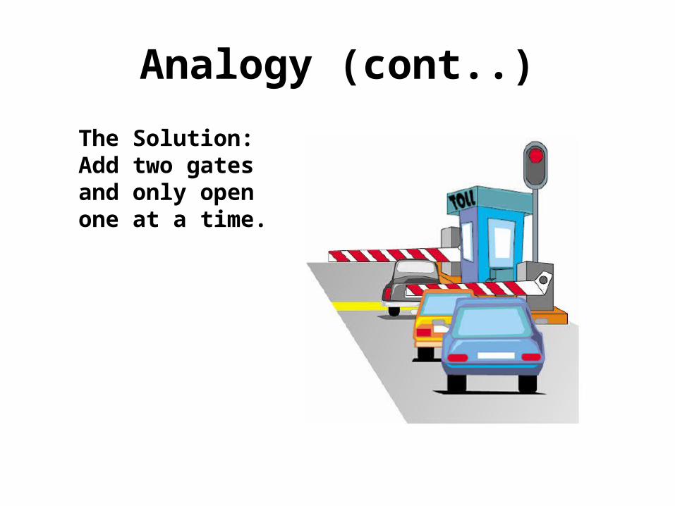
Analogy (cont)
The SolutionAdd two gatesand only openone at a time
Analogy (cont)
The SolutionAdd two gatesand only openone at a time
Analogy (cont)
The SolutionAdd two gatesand only openone at a time
Analogy (cont)
The SolutionAdd two gatesand only openone at a time
Analogy (cont)
The SolutionAdd two gatesand only openone at a time
Analogy (cont)
The SolutionAdd two gatesand only openone at a time
Analogy (cont)
The SolutionAdd two gatesand only openone at a time
Analogy (cont)
The SolutionAdd two gatesand only openone at a time
Edge-triggered Flip FlopThe gate of thislatch is open whenthe clock is low
The gate of thislatch is open whenthe clock is high
master slave
Observationsbull 1048714 only one latch ldquotransparentrdquo at any time
bull 1048714 master closed when slave is openbull 1048714 slave closed when master is openrarr no combinational path through flip flop
bull 1048714 Q only changes shortly after 0 rarr1transition of CLK so flip flop appearsto be ldquotriggeredrdquo by rising edge of CLK
Transitions markinstants not intervals
Flip Flop Waveforms
master slave
CLK
master closedslave open
slave closedmaster open
Um about that hold timehellip
master slave
The masterrsquos contaminationdelay must meet the holdtime of the slave
Consider HOLD TIME requirement for slavebull Negative (1 rarr0) clock transition rarr slave freezes data
bull SHOULD be no output glitch since master held constant data BUTbull master output contaminated by change in G input
bull HOLD TIME of slave not met UNLESS we assume sufficientcontamination delay in the path to its D input
Accumulated tCD thru inverter G rarr Q path of master must coverslave tHOLD for this design to work
Flip Flop Timing - I
tPD maximum propagation delay CLK rarrQtCD minimum contamination delay CLK rarrQ
tSETUP setup timeguarantee that D has propagated through feedback path before master closes
tHOLD hold timeguarantee master is closed and data is stable before allowing D to change
Single-clock Synchronous Circuits
Does thatsymbolregister
Wersquoll use Flip Flops and Registers ndash groups of FFs sharing a clockinput ndash in a highly constrained way to build digitial systems
Single-clock Synchronous Discipline
bull Only care about value of combinationalcircuits just before rising edge ofclock
bull Single clock signal shared amongall clocked devices
bull Period greater than everycombinational delay
Model Discrete TimeNewState
CurrentState
Clock
Input Output
CombinationalLogic
Questionsbull Constraints on TCD for the logic
bull Minimum clock period
bull Setup Hold times for Inputs
SummaryldquoSequentialrdquo Circuits (with memory)
Basic memory elementsbull Feedback detailed analysis =gt basic level-sensitive devices (eg latch)bull 2 Latches =gt Flopbull Dynamic Discipline constraints on input timing
Synchronous 1-clock logicbull Simple rules for sequential circuitsbull Yields clocked circuit with TS TH
constraints on input timing
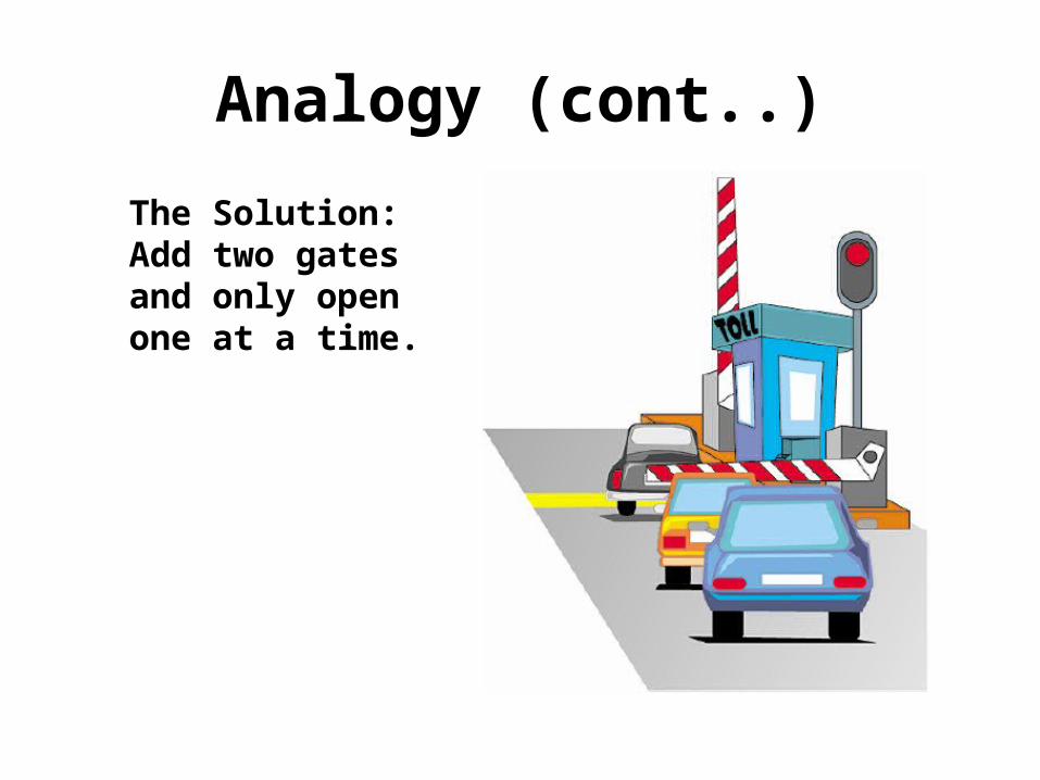
Analogy (cont)
The SolutionAdd two gatesand only openone at a time
Analogy (cont)
The SolutionAdd two gatesand only openone at a time
Analogy (cont)
The SolutionAdd two gatesand only openone at a time
Analogy (cont)
The SolutionAdd two gatesand only openone at a time
Analogy (cont)
The SolutionAdd two gatesand only openone at a time
Analogy (cont)
The SolutionAdd two gatesand only openone at a time
Analogy (cont)
The SolutionAdd two gatesand only openone at a time
Edge-triggered Flip FlopThe gate of thislatch is open whenthe clock is low
The gate of thislatch is open whenthe clock is high
master slave
Observationsbull 1048714 only one latch ldquotransparentrdquo at any time
bull 1048714 master closed when slave is openbull 1048714 slave closed when master is openrarr no combinational path through flip flop
bull 1048714 Q only changes shortly after 0 rarr1transition of CLK so flip flop appearsto be ldquotriggeredrdquo by rising edge of CLK
Transitions markinstants not intervals
Flip Flop Waveforms
master slave
CLK
master closedslave open
slave closedmaster open
Um about that hold timehellip
master slave
The masterrsquos contaminationdelay must meet the holdtime of the slave
Consider HOLD TIME requirement for slavebull Negative (1 rarr0) clock transition rarr slave freezes data
bull SHOULD be no output glitch since master held constant data BUTbull master output contaminated by change in G input
bull HOLD TIME of slave not met UNLESS we assume sufficientcontamination delay in the path to its D input
Accumulated tCD thru inverter G rarr Q path of master must coverslave tHOLD for this design to work
Flip Flop Timing - I
tPD maximum propagation delay CLK rarrQtCD minimum contamination delay CLK rarrQ
tSETUP setup timeguarantee that D has propagated through feedback path before master closes
tHOLD hold timeguarantee master is closed and data is stable before allowing D to change
Single-clock Synchronous Circuits
Does thatsymbolregister
Wersquoll use Flip Flops and Registers ndash groups of FFs sharing a clockinput ndash in a highly constrained way to build digitial systems
Single-clock Synchronous Discipline
bull Only care about value of combinationalcircuits just before rising edge ofclock
bull Single clock signal shared amongall clocked devices
bull Period greater than everycombinational delay
Model Discrete TimeNewState
CurrentState
Clock
Input Output
CombinationalLogic
Questionsbull Constraints on TCD for the logic
bull Minimum clock period
bull Setup Hold times for Inputs
SummaryldquoSequentialrdquo Circuits (with memory)
Basic memory elementsbull Feedback detailed analysis =gt basic level-sensitive devices (eg latch)bull 2 Latches =gt Flopbull Dynamic Discipline constraints on input timing
Synchronous 1-clock logicbull Simple rules for sequential circuitsbull Yields clocked circuit with TS TH
constraints on input timing
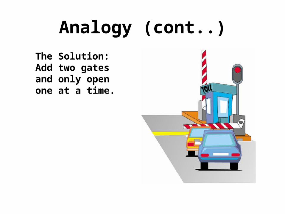
Analogy (cont)
The SolutionAdd two gatesand only openone at a time
Analogy (cont)
The SolutionAdd two gatesand only openone at a time
Analogy (cont)
The SolutionAdd two gatesand only openone at a time
Analogy (cont)
The SolutionAdd two gatesand only openone at a time
Analogy (cont)
The SolutionAdd two gatesand only openone at a time
Analogy (cont)
The SolutionAdd two gatesand only openone at a time
Edge-triggered Flip FlopThe gate of thislatch is open whenthe clock is low
The gate of thislatch is open whenthe clock is high
master slave
Observationsbull 1048714 only one latch ldquotransparentrdquo at any time
bull 1048714 master closed when slave is openbull 1048714 slave closed when master is openrarr no combinational path through flip flop
bull 1048714 Q only changes shortly after 0 rarr1transition of CLK so flip flop appearsto be ldquotriggeredrdquo by rising edge of CLK
Transitions markinstants not intervals
Flip Flop Waveforms
master slave
CLK
master closedslave open
slave closedmaster open
Um about that hold timehellip
master slave
The masterrsquos contaminationdelay must meet the holdtime of the slave
Consider HOLD TIME requirement for slavebull Negative (1 rarr0) clock transition rarr slave freezes data
bull SHOULD be no output glitch since master held constant data BUTbull master output contaminated by change in G input
bull HOLD TIME of slave not met UNLESS we assume sufficientcontamination delay in the path to its D input
Accumulated tCD thru inverter G rarr Q path of master must coverslave tHOLD for this design to work
Flip Flop Timing - I
tPD maximum propagation delay CLK rarrQtCD minimum contamination delay CLK rarrQ
tSETUP setup timeguarantee that D has propagated through feedback path before master closes
tHOLD hold timeguarantee master is closed and data is stable before allowing D to change
Single-clock Synchronous Circuits
Does thatsymbolregister
Wersquoll use Flip Flops and Registers ndash groups of FFs sharing a clockinput ndash in a highly constrained way to build digitial systems
Single-clock Synchronous Discipline
bull Only care about value of combinationalcircuits just before rising edge ofclock
bull Single clock signal shared amongall clocked devices
bull Period greater than everycombinational delay
Model Discrete TimeNewState
CurrentState
Clock
Input Output
CombinationalLogic
Questionsbull Constraints on TCD for the logic
bull Minimum clock period
bull Setup Hold times for Inputs
SummaryldquoSequentialrdquo Circuits (with memory)
Basic memory elementsbull Feedback detailed analysis =gt basic level-sensitive devices (eg latch)bull 2 Latches =gt Flopbull Dynamic Discipline constraints on input timing
Synchronous 1-clock logicbull Simple rules for sequential circuitsbull Yields clocked circuit with TS TH
constraints on input timing
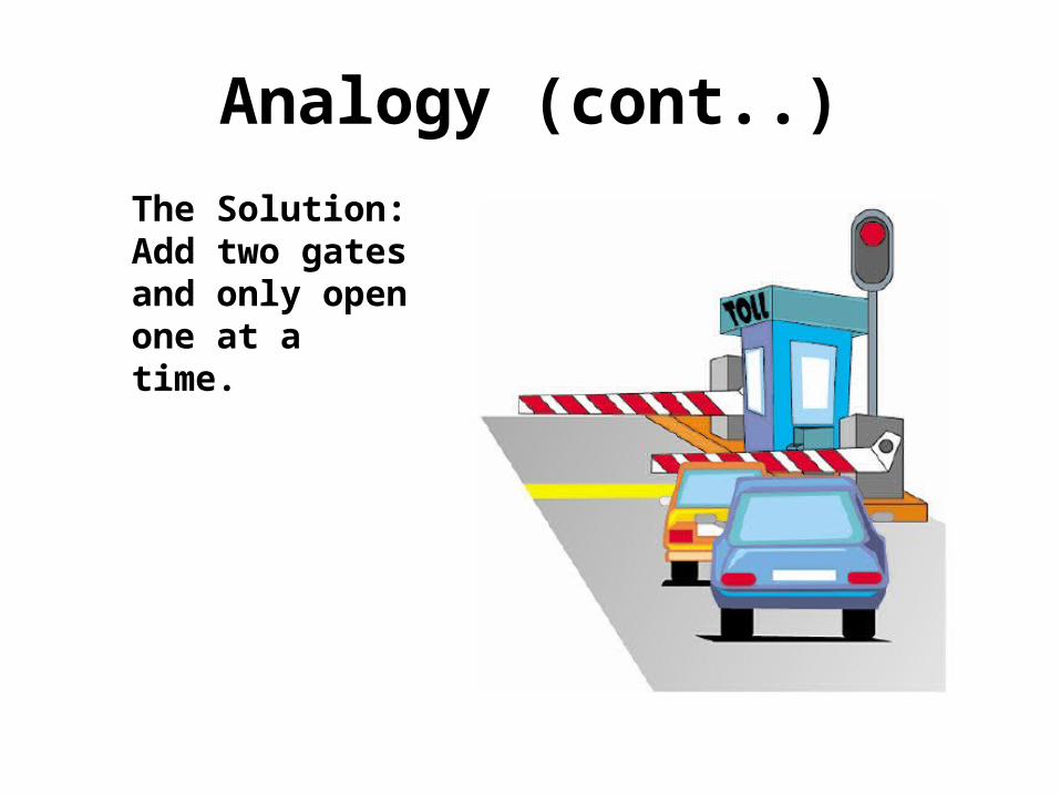
Analogy (cont)
The SolutionAdd two gatesand only openone at a time
Analogy (cont)
The SolutionAdd two gatesand only openone at a time
Analogy (cont)
The SolutionAdd two gatesand only openone at a time
Analogy (cont)
The SolutionAdd two gatesand only openone at a time
Analogy (cont)
The SolutionAdd two gatesand only openone at a time
Edge-triggered Flip FlopThe gate of thislatch is open whenthe clock is low
The gate of thislatch is open whenthe clock is high
master slave
Observationsbull 1048714 only one latch ldquotransparentrdquo at any time
bull 1048714 master closed when slave is openbull 1048714 slave closed when master is openrarr no combinational path through flip flop
bull 1048714 Q only changes shortly after 0 rarr1transition of CLK so flip flop appearsto be ldquotriggeredrdquo by rising edge of CLK
Transitions markinstants not intervals
Flip Flop Waveforms
master slave
CLK
master closedslave open
slave closedmaster open
Um about that hold timehellip
master slave
The masterrsquos contaminationdelay must meet the holdtime of the slave
Consider HOLD TIME requirement for slavebull Negative (1 rarr0) clock transition rarr slave freezes data
bull SHOULD be no output glitch since master held constant data BUTbull master output contaminated by change in G input
bull HOLD TIME of slave not met UNLESS we assume sufficientcontamination delay in the path to its D input
Accumulated tCD thru inverter G rarr Q path of master must coverslave tHOLD for this design to work
Flip Flop Timing - I
tPD maximum propagation delay CLK rarrQtCD minimum contamination delay CLK rarrQ
tSETUP setup timeguarantee that D has propagated through feedback path before master closes
tHOLD hold timeguarantee master is closed and data is stable before allowing D to change
Single-clock Synchronous Circuits
Does thatsymbolregister
Wersquoll use Flip Flops and Registers ndash groups of FFs sharing a clockinput ndash in a highly constrained way to build digitial systems
Single-clock Synchronous Discipline
bull Only care about value of combinationalcircuits just before rising edge ofclock
bull Single clock signal shared amongall clocked devices
bull Period greater than everycombinational delay
Model Discrete TimeNewState
CurrentState
Clock
Input Output
CombinationalLogic
Questionsbull Constraints on TCD for the logic
bull Minimum clock period
bull Setup Hold times for Inputs
SummaryldquoSequentialrdquo Circuits (with memory)
Basic memory elementsbull Feedback detailed analysis =gt basic level-sensitive devices (eg latch)bull 2 Latches =gt Flopbull Dynamic Discipline constraints on input timing
Synchronous 1-clock logicbull Simple rules for sequential circuitsbull Yields clocked circuit with TS TH
constraints on input timing
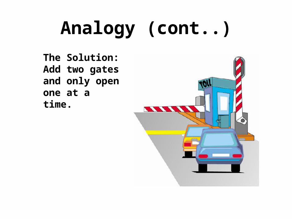
Analogy (cont)
The SolutionAdd two gatesand only openone at a time
Analogy (cont)
The SolutionAdd two gatesand only openone at a time
Analogy (cont)
The SolutionAdd two gatesand only openone at a time
Analogy (cont)
The SolutionAdd two gatesand only openone at a time
Edge-triggered Flip FlopThe gate of thislatch is open whenthe clock is low
The gate of thislatch is open whenthe clock is high
master slave
Observationsbull 1048714 only one latch ldquotransparentrdquo at any time
bull 1048714 master closed when slave is openbull 1048714 slave closed when master is openrarr no combinational path through flip flop
bull 1048714 Q only changes shortly after 0 rarr1transition of CLK so flip flop appearsto be ldquotriggeredrdquo by rising edge of CLK
Transitions markinstants not intervals
Flip Flop Waveforms
master slave
CLK
master closedslave open
slave closedmaster open
Um about that hold timehellip
master slave
The masterrsquos contaminationdelay must meet the holdtime of the slave
Consider HOLD TIME requirement for slavebull Negative (1 rarr0) clock transition rarr slave freezes data
bull SHOULD be no output glitch since master held constant data BUTbull master output contaminated by change in G input
bull HOLD TIME of slave not met UNLESS we assume sufficientcontamination delay in the path to its D input
Accumulated tCD thru inverter G rarr Q path of master must coverslave tHOLD for this design to work
Flip Flop Timing - I
tPD maximum propagation delay CLK rarrQtCD minimum contamination delay CLK rarrQ
tSETUP setup timeguarantee that D has propagated through feedback path before master closes
tHOLD hold timeguarantee master is closed and data is stable before allowing D to change
Single-clock Synchronous Circuits
Does thatsymbolregister
Wersquoll use Flip Flops and Registers ndash groups of FFs sharing a clockinput ndash in a highly constrained way to build digitial systems
Single-clock Synchronous Discipline
bull Only care about value of combinationalcircuits just before rising edge ofclock
bull Single clock signal shared amongall clocked devices
bull Period greater than everycombinational delay
Model Discrete TimeNewState
CurrentState
Clock
Input Output
CombinationalLogic
Questionsbull Constraints on TCD for the logic
bull Minimum clock period
bull Setup Hold times for Inputs
SummaryldquoSequentialrdquo Circuits (with memory)
Basic memory elementsbull Feedback detailed analysis =gt basic level-sensitive devices (eg latch)bull 2 Latches =gt Flopbull Dynamic Discipline constraints on input timing
Synchronous 1-clock logicbull Simple rules for sequential circuitsbull Yields clocked circuit with TS TH
constraints on input timing
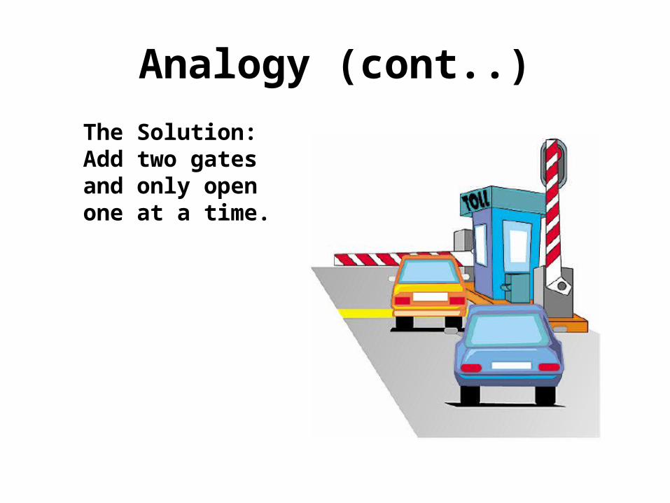
Analogy (cont)
The SolutionAdd two gatesand only openone at a time
Analogy (cont)
The SolutionAdd two gatesand only openone at a time
Analogy (cont)
The SolutionAdd two gatesand only openone at a time
Edge-triggered Flip FlopThe gate of thislatch is open whenthe clock is low
The gate of thislatch is open whenthe clock is high
master slave
Observationsbull 1048714 only one latch ldquotransparentrdquo at any time
bull 1048714 master closed when slave is openbull 1048714 slave closed when master is openrarr no combinational path through flip flop
bull 1048714 Q only changes shortly after 0 rarr1transition of CLK so flip flop appearsto be ldquotriggeredrdquo by rising edge of CLK
Transitions markinstants not intervals
Flip Flop Waveforms
master slave
CLK
master closedslave open
slave closedmaster open
Um about that hold timehellip
master slave
The masterrsquos contaminationdelay must meet the holdtime of the slave
Consider HOLD TIME requirement for slavebull Negative (1 rarr0) clock transition rarr slave freezes data
bull SHOULD be no output glitch since master held constant data BUTbull master output contaminated by change in G input
bull HOLD TIME of slave not met UNLESS we assume sufficientcontamination delay in the path to its D input
Accumulated tCD thru inverter G rarr Q path of master must coverslave tHOLD for this design to work
Flip Flop Timing - I
tPD maximum propagation delay CLK rarrQtCD minimum contamination delay CLK rarrQ
tSETUP setup timeguarantee that D has propagated through feedback path before master closes
tHOLD hold timeguarantee master is closed and data is stable before allowing D to change
Single-clock Synchronous Circuits
Does thatsymbolregister
Wersquoll use Flip Flops and Registers ndash groups of FFs sharing a clockinput ndash in a highly constrained way to build digitial systems
Single-clock Synchronous Discipline
bull Only care about value of combinationalcircuits just before rising edge ofclock
bull Single clock signal shared amongall clocked devices
bull Period greater than everycombinational delay
Model Discrete TimeNewState
CurrentState
Clock
Input Output
CombinationalLogic
Questionsbull Constraints on TCD for the logic
bull Minimum clock period
bull Setup Hold times for Inputs
SummaryldquoSequentialrdquo Circuits (with memory)
Basic memory elementsbull Feedback detailed analysis =gt basic level-sensitive devices (eg latch)bull 2 Latches =gt Flopbull Dynamic Discipline constraints on input timing
Synchronous 1-clock logicbull Simple rules for sequential circuitsbull Yields clocked circuit with TS TH
constraints on input timing
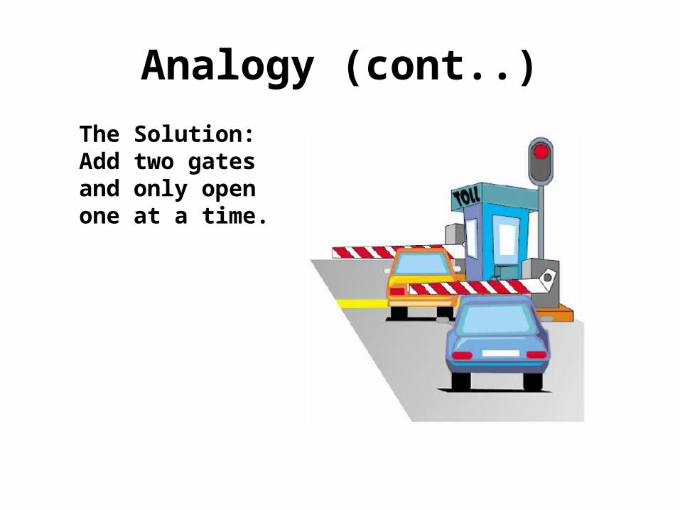
Analogy (cont)
The SolutionAdd two gatesand only openone at a time
Analogy (cont)
The SolutionAdd two gatesand only openone at a time
Edge-triggered Flip FlopThe gate of thislatch is open whenthe clock is low
The gate of thislatch is open whenthe clock is high
master slave
Observationsbull 1048714 only one latch ldquotransparentrdquo at any time
bull 1048714 master closed when slave is openbull 1048714 slave closed when master is openrarr no combinational path through flip flop
bull 1048714 Q only changes shortly after 0 rarr1transition of CLK so flip flop appearsto be ldquotriggeredrdquo by rising edge of CLK
Transitions markinstants not intervals
Flip Flop Waveforms
master slave
CLK
master closedslave open
slave closedmaster open
Um about that hold timehellip
master slave
The masterrsquos contaminationdelay must meet the holdtime of the slave
Consider HOLD TIME requirement for slavebull Negative (1 rarr0) clock transition rarr slave freezes data
bull SHOULD be no output glitch since master held constant data BUTbull master output contaminated by change in G input
bull HOLD TIME of slave not met UNLESS we assume sufficientcontamination delay in the path to its D input
Accumulated tCD thru inverter G rarr Q path of master must coverslave tHOLD for this design to work
Flip Flop Timing - I
tPD maximum propagation delay CLK rarrQtCD minimum contamination delay CLK rarrQ
tSETUP setup timeguarantee that D has propagated through feedback path before master closes
tHOLD hold timeguarantee master is closed and data is stable before allowing D to change
Single-clock Synchronous Circuits
Does thatsymbolregister
Wersquoll use Flip Flops and Registers ndash groups of FFs sharing a clockinput ndash in a highly constrained way to build digitial systems
Single-clock Synchronous Discipline
bull Only care about value of combinationalcircuits just before rising edge ofclock
bull Single clock signal shared amongall clocked devices
bull Period greater than everycombinational delay
Model Discrete TimeNewState
CurrentState
Clock
Input Output
CombinationalLogic
Questionsbull Constraints on TCD for the logic
bull Minimum clock period
bull Setup Hold times for Inputs
SummaryldquoSequentialrdquo Circuits (with memory)
Basic memory elementsbull Feedback detailed analysis =gt basic level-sensitive devices (eg latch)bull 2 Latches =gt Flopbull Dynamic Discipline constraints on input timing
Synchronous 1-clock logicbull Simple rules for sequential circuitsbull Yields clocked circuit with TS TH
constraints on input timing
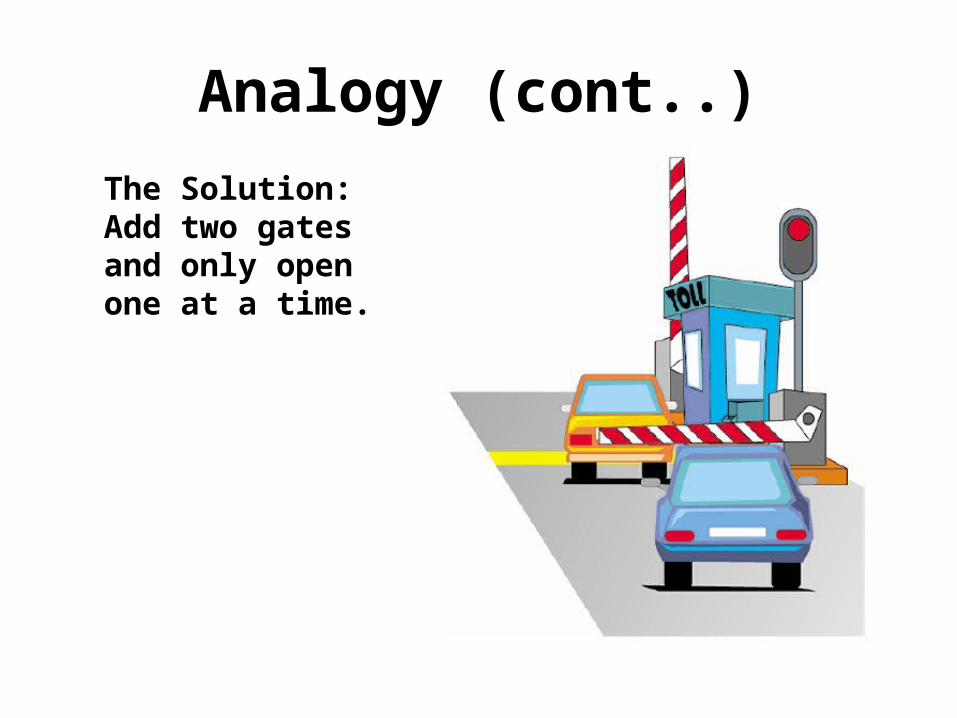
Analogy (cont)
The SolutionAdd two gatesand only openone at a time
Edge-triggered Flip FlopThe gate of thislatch is open whenthe clock is low
The gate of thislatch is open whenthe clock is high
master slave
Observationsbull 1048714 only one latch ldquotransparentrdquo at any time
bull 1048714 master closed when slave is openbull 1048714 slave closed when master is openrarr no combinational path through flip flop
bull 1048714 Q only changes shortly after 0 rarr1transition of CLK so flip flop appearsto be ldquotriggeredrdquo by rising edge of CLK
Transitions markinstants not intervals
Flip Flop Waveforms
master slave
CLK
master closedslave open
slave closedmaster open
Um about that hold timehellip
master slave
The masterrsquos contaminationdelay must meet the holdtime of the slave
Consider HOLD TIME requirement for slavebull Negative (1 rarr0) clock transition rarr slave freezes data
bull SHOULD be no output glitch since master held constant data BUTbull master output contaminated by change in G input
bull HOLD TIME of slave not met UNLESS we assume sufficientcontamination delay in the path to its D input
Accumulated tCD thru inverter G rarr Q path of master must coverslave tHOLD for this design to work
Flip Flop Timing - I
tPD maximum propagation delay CLK rarrQtCD minimum contamination delay CLK rarrQ
tSETUP setup timeguarantee that D has propagated through feedback path before master closes
tHOLD hold timeguarantee master is closed and data is stable before allowing D to change
Single-clock Synchronous Circuits
Does thatsymbolregister
Wersquoll use Flip Flops and Registers ndash groups of FFs sharing a clockinput ndash in a highly constrained way to build digitial systems
Single-clock Synchronous Discipline
bull Only care about value of combinationalcircuits just before rising edge ofclock
bull Single clock signal shared amongall clocked devices
bull Period greater than everycombinational delay
Model Discrete TimeNewState
CurrentState
Clock
Input Output
CombinationalLogic
Questionsbull Constraints on TCD for the logic
bull Minimum clock period
bull Setup Hold times for Inputs
SummaryldquoSequentialrdquo Circuits (with memory)
Basic memory elementsbull Feedback detailed analysis =gt basic level-sensitive devices (eg latch)bull 2 Latches =gt Flopbull Dynamic Discipline constraints on input timing
Synchronous 1-clock logicbull Simple rules for sequential circuitsbull Yields clocked circuit with TS TH
constraints on input timing
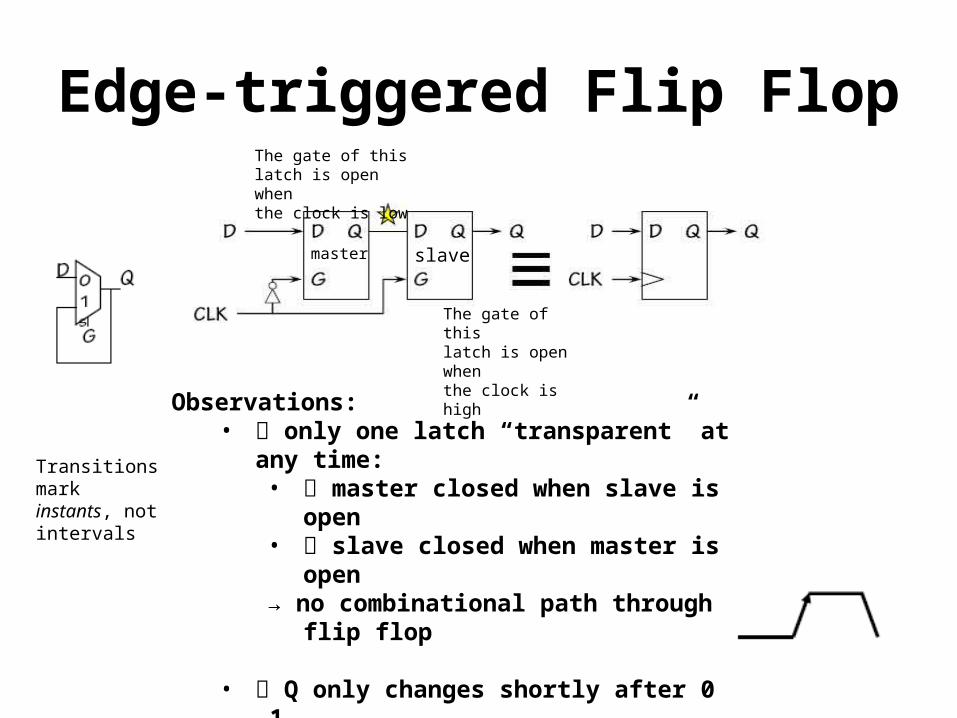
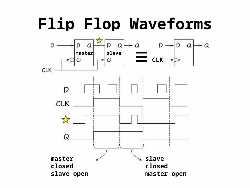
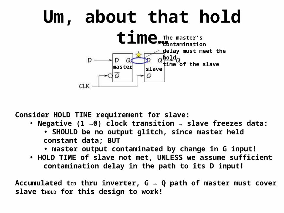
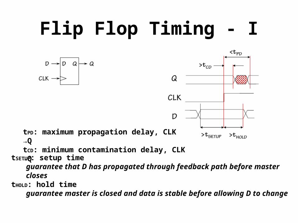
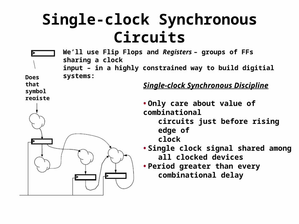
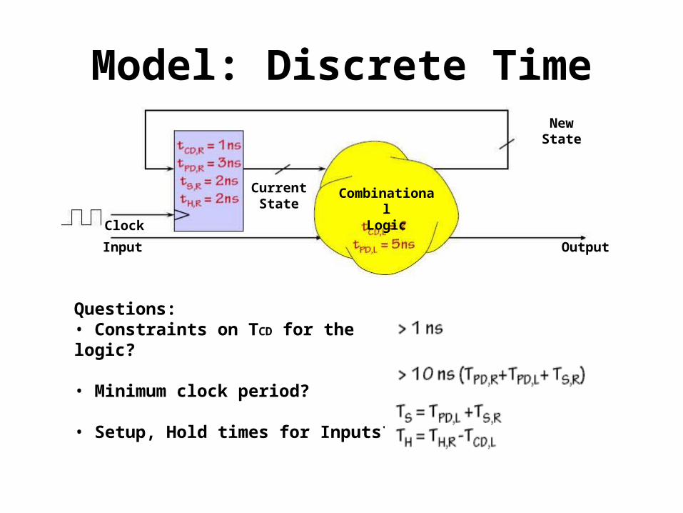
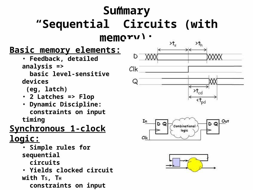