Embed Size (px)
Citation preview
1
Computer Architecture
Lecture 1Naohiko
Shimizu

2
What is the Architecture?
•
It came from the arch of buildings. The structure, design etc.
Computer Architecture
3
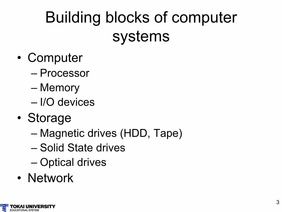
Building blocks of computer systems
•
Computer–
Processor
–
Memory–
I/O devices
•
Storage–
Magnetic drives (HDD, Tape)
–
Solid State drives–
Optical drives
•
Network
4
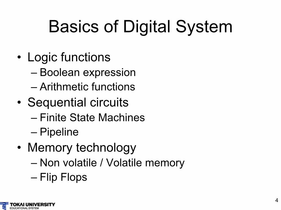
Basics of Digital System•
Logic functions–
Boolean expression
–
Arithmetic functions•
Sequential circuits–
Finite State Machines
–
Pipeline•
Memory technology–
Non volatile / Volatile memory
–
Flip Flops
5
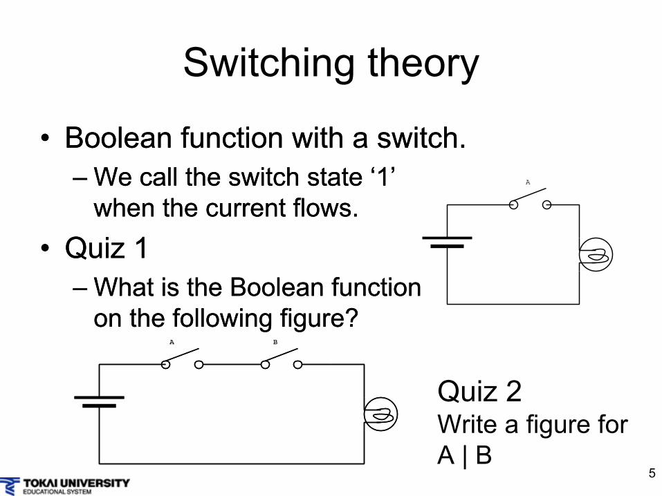
Switching theory
•
Boolean function with a switch.–
We call the switch state ‘1’
when the current flows.•
Quiz 1–
What is the Boolean function
on the following figure?
A
A B
Quiz 2Write a figure forA | B
•
Boolean function with a switch.–
We call the switch state ‘1’
when the current flows.•
Quiz 1–
What is the Boolean function
on the following figure?A B
6
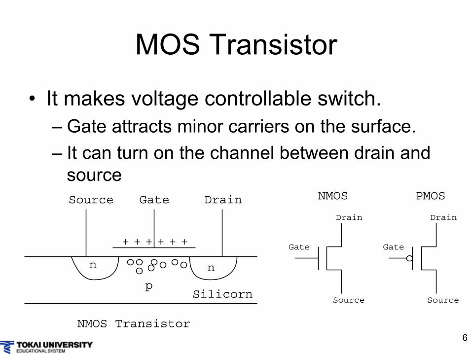
MOS Transistor
•
It makes voltage controllable switch.–
Gate attracts minor carriers on the surface.
–
It can turn on the channel between drain and source
Gate DrainSource
Silicorn
n n
p
NMOS Transistor
+
-- - - ----
+ + + + +Gate
Drain
Source
Gate
Drain
Source
NMOS PMOS
7
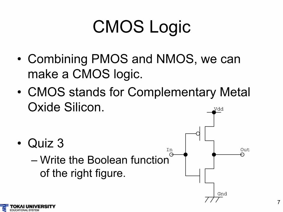
CMOS Logic
•
Combining PMOS and NMOS, we can make a CMOS logic.
•
CMOS stands for Complementary Metal Oxide Silicon.
•
Quiz 3–
Write the Boolean function
of the right figure.
Vdd
Gnd
In Out
8
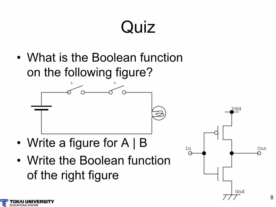
Quiz
•
What is the Boolean function on the following figure?
•
Write a figure for A | B•
Write the Boolean function
of the right figure
A B
Vdd
Gnd
In Out
1
Computer Architecture
Lecture 2CMOS Logic Ciurcuits
2
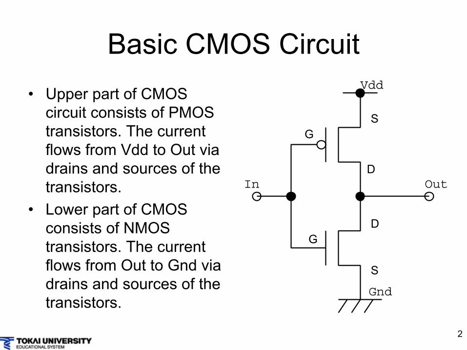
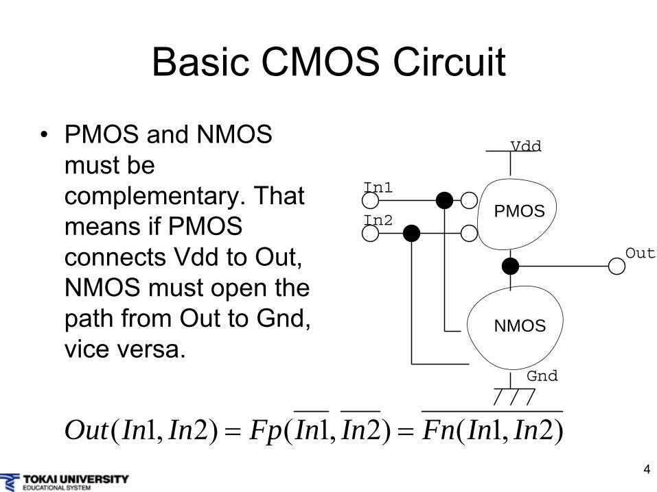
Basic CMOS Circuit•
Upper part of CMOS circuit consists of PMOS transistors. The current flows from Vdd
to Out via
drains and sources of the transistors.
•
Lower part of CMOS consists of NMOS transistors. The current flows from Out to Gnd
via
drains and sources of the transistors.
Vdd
Gnd
In Out
D
S
G
D
SG
3
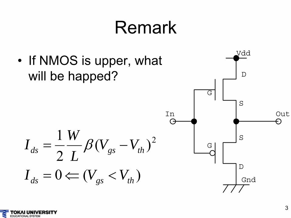
Remark
•
If NMOS is upper, what will be happed?
Vdd
Gnd
In Out
D
S
G
S
D
G
)(0
)(21 2
thgsds
thgsds
VVI
VVLWI
4
Basic CMOS Circuit•
PMOS and NMOS must be complementary. That means if PMOS connects Vdd
to Out,
NMOS must open the path from Out to Gnd, vice versa.
Vdd
Gnd
Out
In1
In2 PMOS
NMOS
)2,1()2,1()2,1( InInFnInInFpInInOut
5
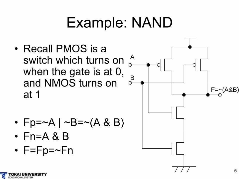
Example: NAND•
Recall PMOS is a switch which turns on when the gate is at 0, and NMOS turns on at 1
•
Fp=~A | ~B=~(A & B)•
Fn=A & B
•
F=Fp=~Fn
A
B
F=~(A&B)
6
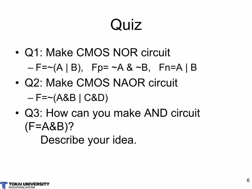
Quiz
•
Q1: Make CMOS NOR circuit–
F=~(A | B), Fp= ~A & ~B, Fn=A | B
•
Q2: Make CMOS NAOR circuit–
F=~(A&B | C&D)
•
Q3: How can you make AND circuit (F=A&B)?
Describe your idea.
1
Computer Architecture
Lecture 3Latch: memorize the data
2
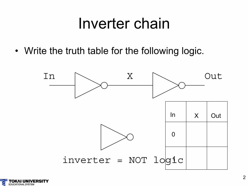
Inverter chain•
Write the truth table for the following logic.
In OutX
inverter = NOT logic
In X Out
0
1
3
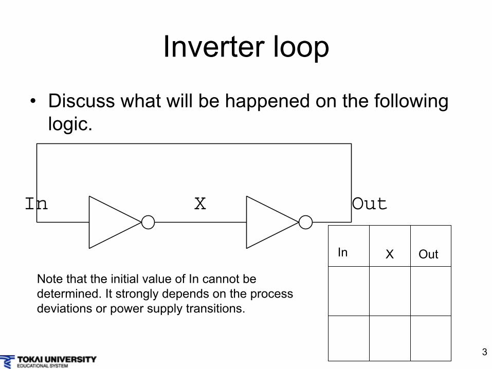
Inverter loop•
Discuss what will be happened on the following logic.
In X Out
In OutX
Note that the initial value of In cannot be determined. It strongly depends on the process deviations or power supply transitions.
4
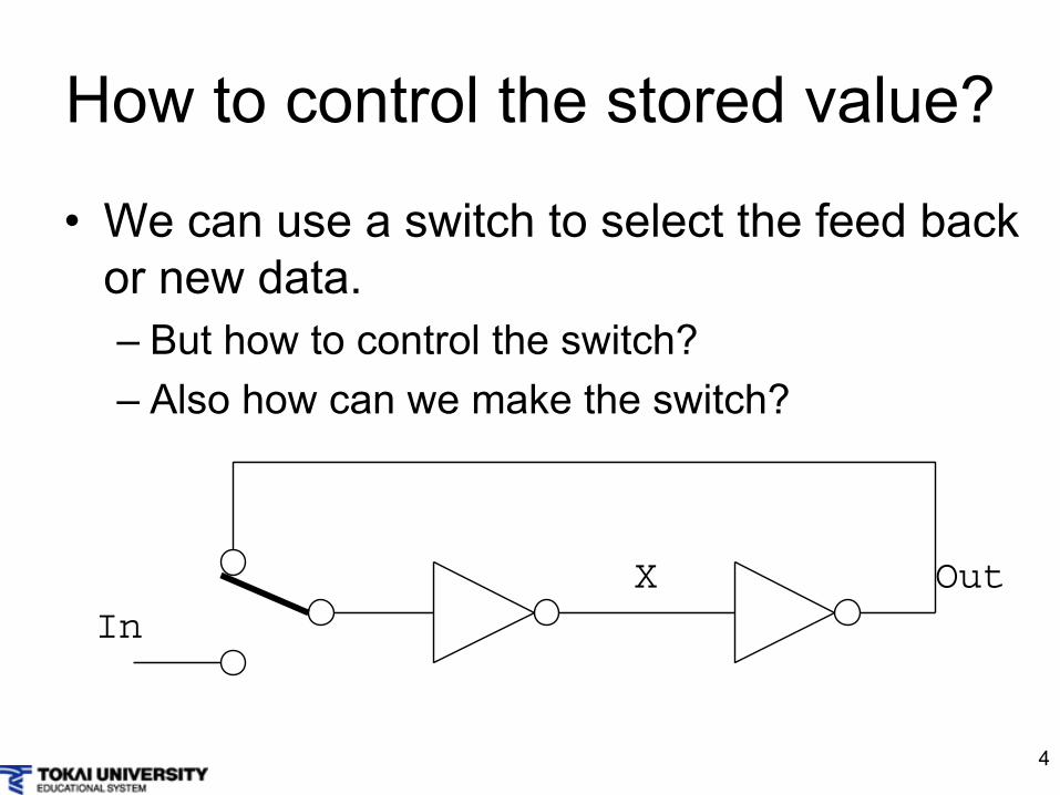
How to control the stored value?
•
We can use a switch to select the feed back or new data.–
But how to control the switch?
–
Also how can we make the switch?
InOutX
5
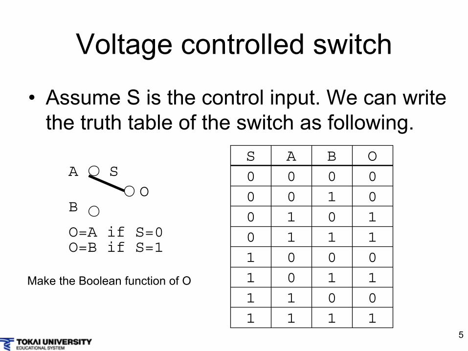
Voltage controlled switch
•
Assume S is the control input. We can write the truth table of the switch as following.
A
BO
S
O=A if S=0O=B if S=1
S A B O0 0 0 00 0 1 00 1 0 10 1 1 11 0 0 01 0 1 11 1 0 01 1 1 1
Make the Boolean function of O
6
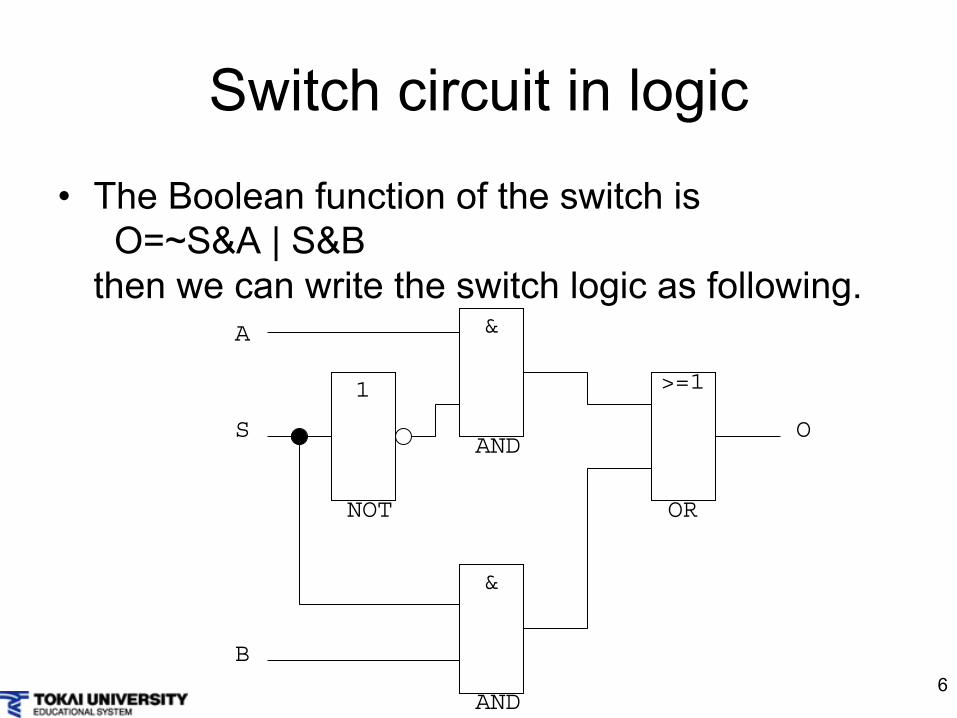
Switch circuit in logic•
The Boolean function of the switch is
O=~S&A | S&B then we can write the switch logic as following.
&
AND
>=1
OR
&
AND
1
NOT
A
S
B
O
7
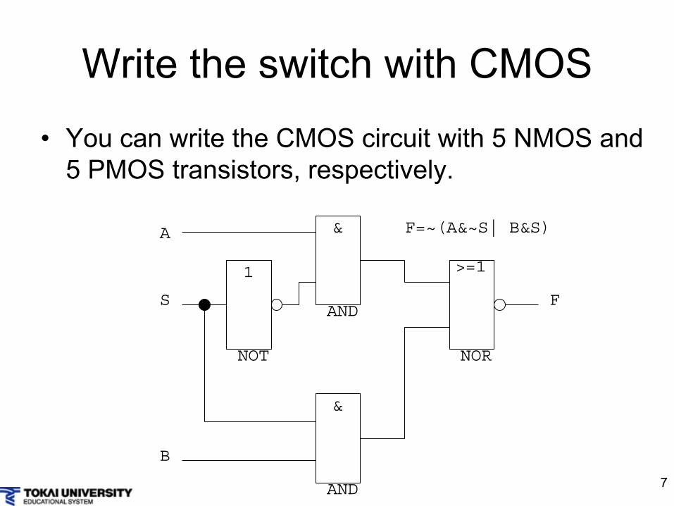
Write the switch with CMOS•
You can write the CMOS circuit with 5 NMOS and 5 PMOS transistors, respectively.
&
AND
>=1
NOR
&
AND
1
NOT
A
S
B
F
F=~(A&~S| B&S)
8
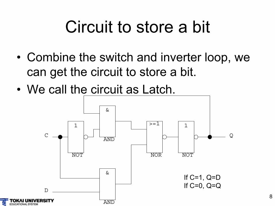
Circuit to store a bit
•
Combine the switch and inverter loop, we can get the circuit to store a bit.
•
We call the circuit as Latch.&
AND
&
AND
1
NOT
C
D
>=1
NOR
1
NOT
Q
If C=1, Q=DIf C=0, Q=Q
9
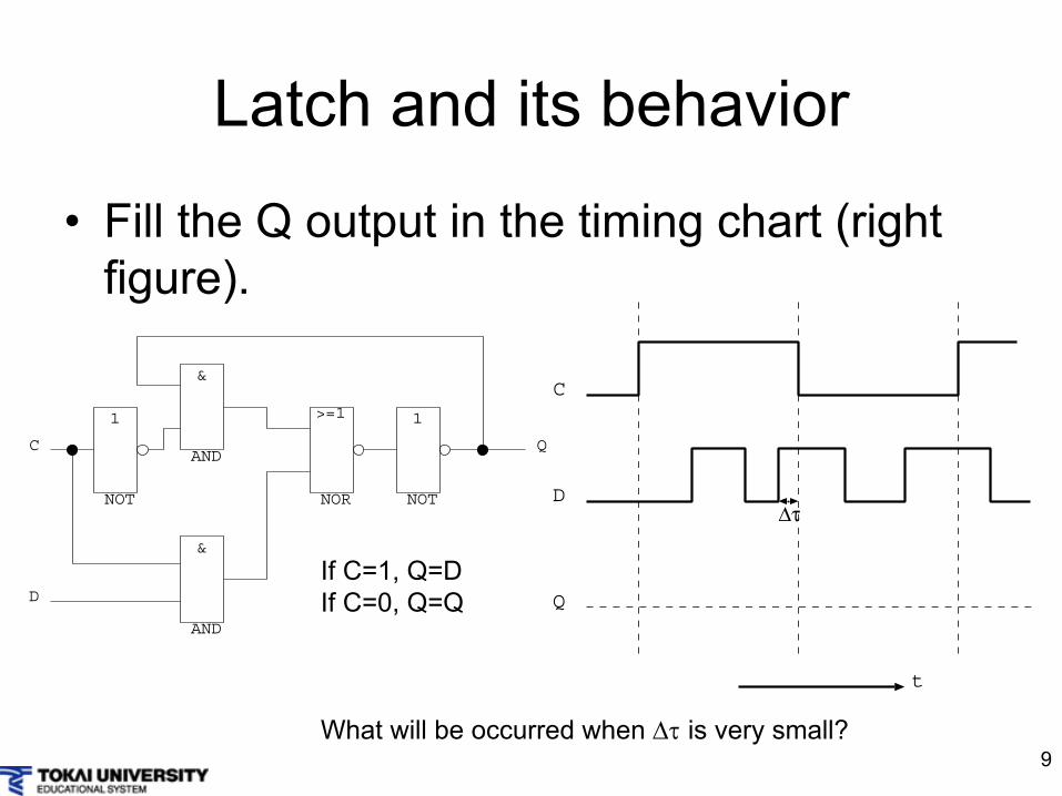
Latch and its behavior
•
Fill the Q output in the timing chart (right figure).
&
AND
&
AND
1
NOT
C
D
>=1
NOR
1
NOT
Q
If C=1, Q=DIf C=0, Q=Q
C
D
Q
t
Δτ
What will be occurred when
is very small?
10
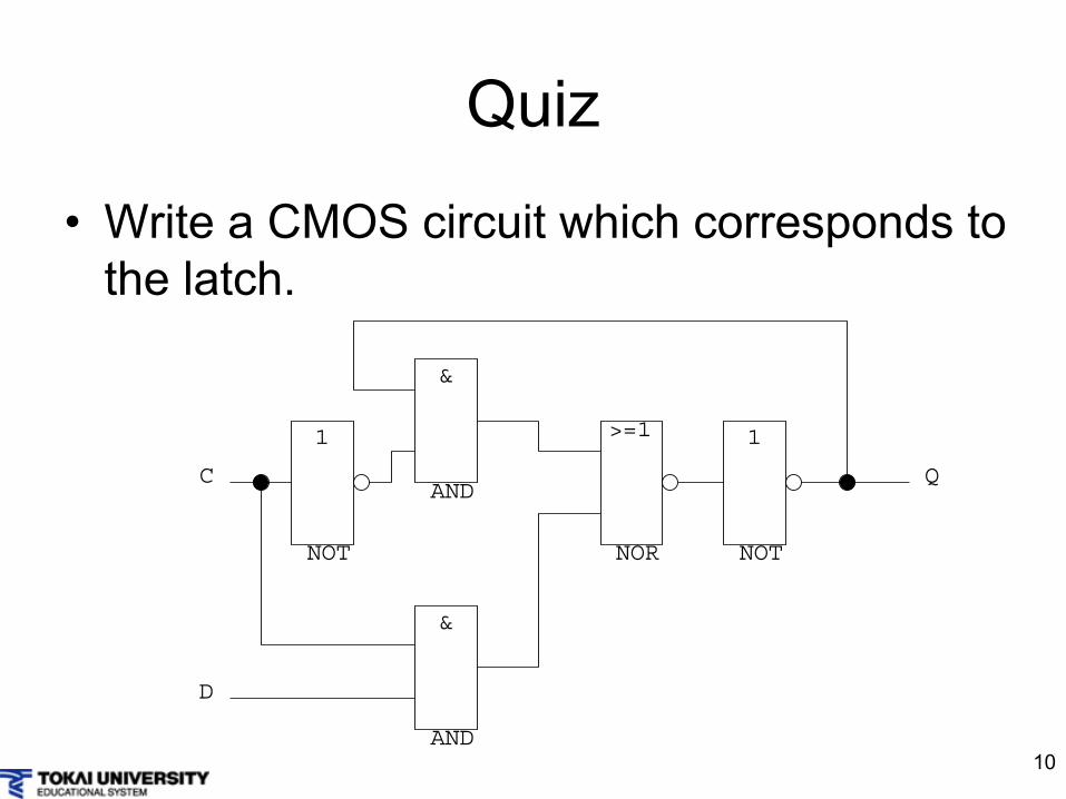
Quiz
•
Write a CMOS circuit which corresponds to the latch.
&
AND
&
AND
1
NOT
C
D
>=1
NOR
1
NOT
Q
1
Computer Architecture
Lecture 4Flip Flop
2
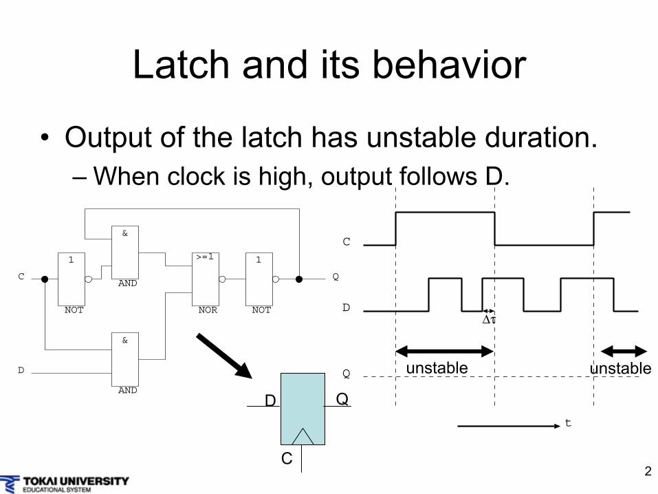
Latch and its behavior
•
Output of the latch has unstable duration.–
When clock is high, output follows D.
&
AND
&
AND
1
NOT
C
D
>=1
NOR
1
NOT
Q
C
D
Q
t
Δτ
unstable unstable
D Q
C
3
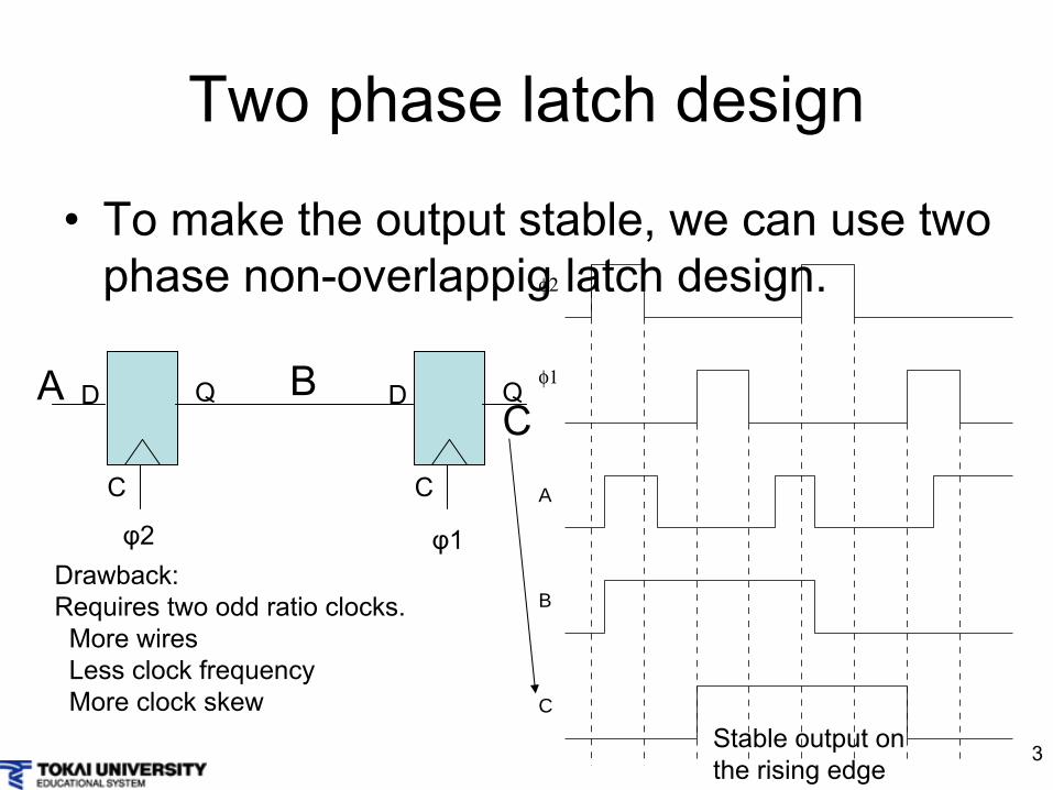
Two phase latch design
•
To make the output stable, we can use two phase non-overlappig
latch design.
D Q
C
D Q
C
φ2 φ1
A BC
Drawback:Requires two odd ratio clocks.More wiresLess clock frequencyMore clock skew
φ2
φ1
A
B
C
Stable output on
the rising edge
4
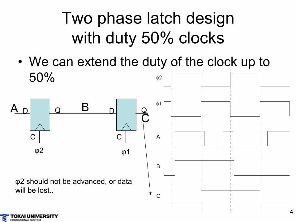
Two phase latch design with duty 50% clocks
•
We can extend the duty of the clock up to 50%
D Q
C
D Q
C
φ2 φ1
A BC
φ2 should not be advanced, or data will be lost..
φ2
φ1
A
B
C
5
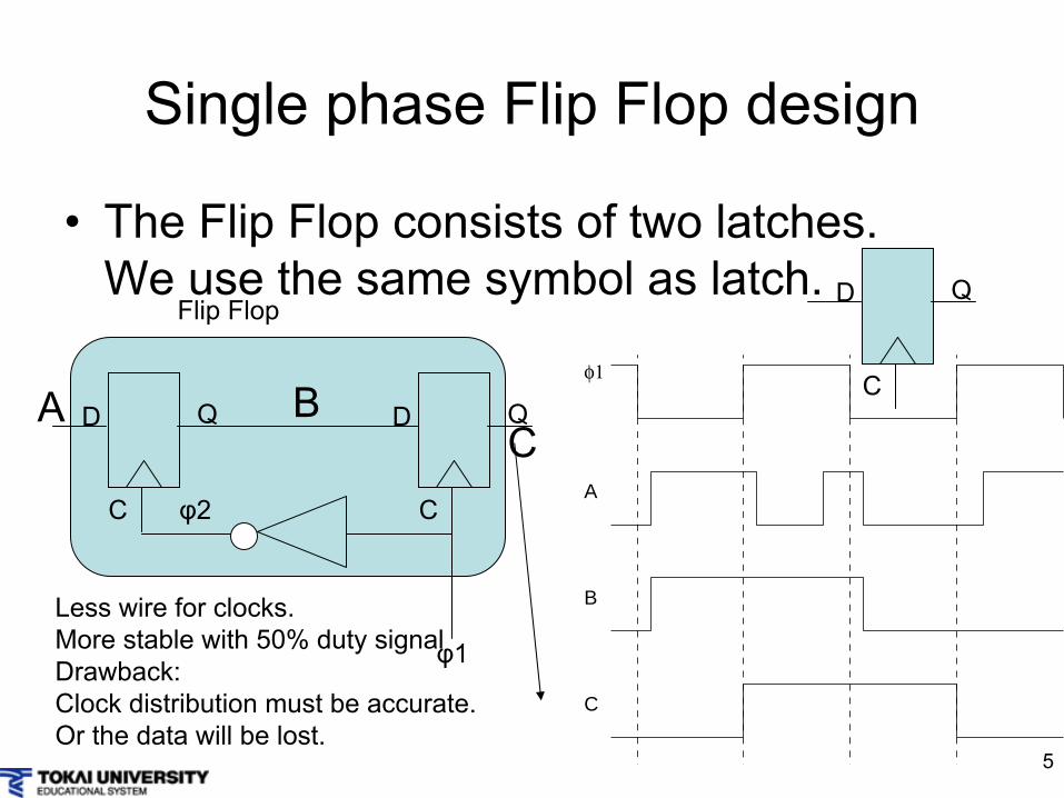
Single phase Flip Flop design
D Q
C
D Q
C
φ1
A BC
Less wire for clocks.More stable with 50% duty signalDrawback:Clock distribution must be accurate.Or the data will be lost.
φ2
φ1
A
B
C
φ2
Flip Flop D Q
C
•
The Flip Flop consists of two latches. We use the same symbol as latch.
6
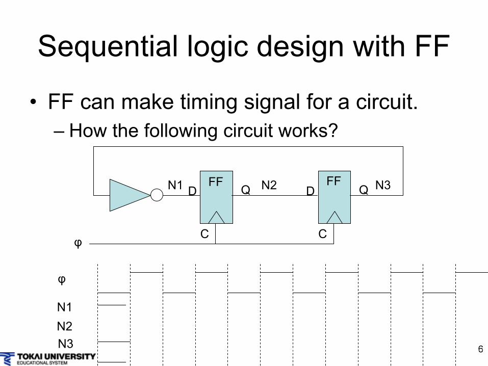
Sequential logic design with FF
•
FF can make timing signal for a circuit.–
How the following circuit works?
D Q
C
D Q
Cφ
FF FFN1 N2 N3
φ
N1N2N3
7
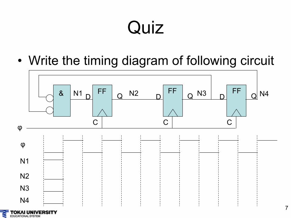
Quiz
•
Write the timing diagram of following circuit
D Q
C
D Q
Cφ
FF FFN1 N2 N3
φ
N1
N2N3
D Q
C
N4
N4
FF&

1
Computer Architecture
Lecture 5State Machines
2
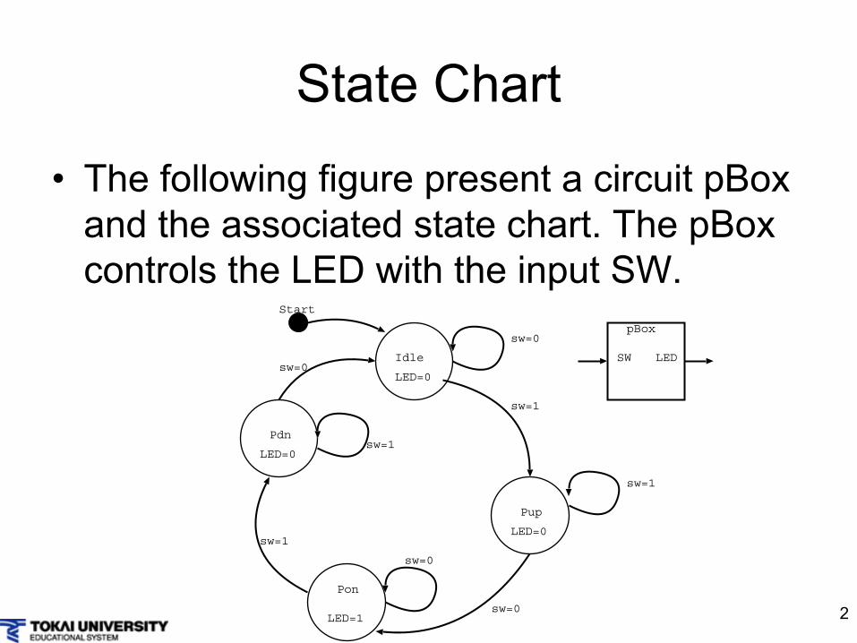
State Chart
•
The following figure present a circuit pBox and the associated state chart. The pBox
controls the LED with the input SW.Start
Idle
Pup
Pon
sw=0
sw=1
sw=1
sw=0
Pdnsw=1
sw=0
sw=0
sw=1
SW LED
LED=0
LED=0
LED=1
LED=0
pBox
3
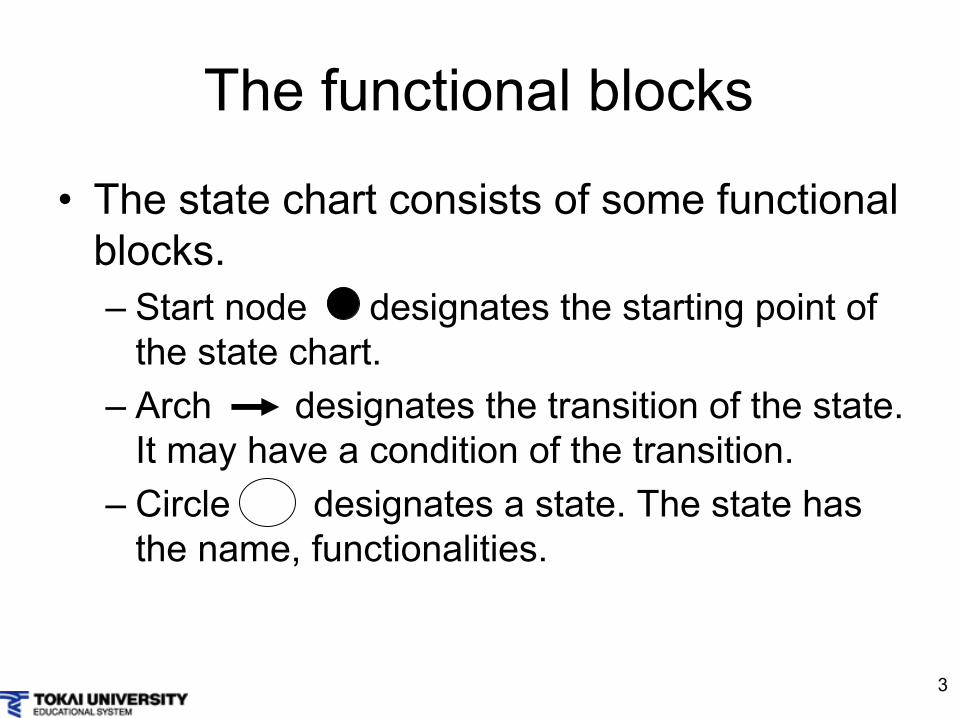
The functional blocks
•
The state chart consists of some functional blocks.–
Start node designates the starting point of the state chart.
–
Arch designates the transition of the state. It may have a condition of the transition.
–
Circle designates a state. The state has the name, functionalities.
4
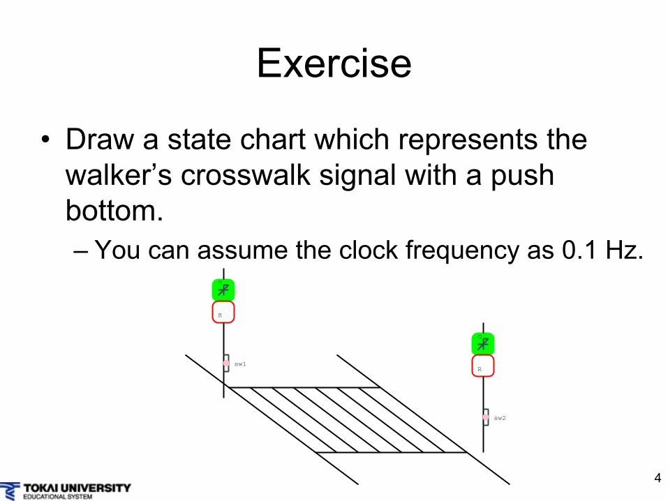
Exercise
•
Draw a state chart which represents the walker’s crosswalk signal with a push bottom.–
You can assume the clock frequency as 0.1 Hz.
sw1
sw2
R
G
R
G
5
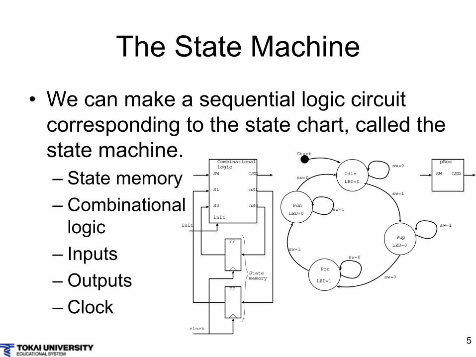
The State Machine
•
We can make a sequential logic circuit corresponding to the state chart, called the state machine.–
State memory
–
Combinational logic
–
Inputs–
Outputs
–
Clock
Start
Idle
Pup
Pon
sw=0
sw=1
sw=1
sw=0
Pdnsw=1
sw=0
sw=0
sw=1
SW LED
LED=0
LED=0
LED=1
LED=0
pBox
SW LED
S1 nS1
S0 nS0
FF
FF
Combinationallogic
init
clock
init
Statememory
6
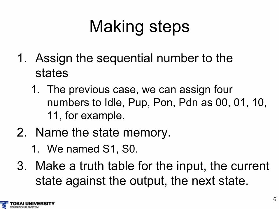
Making steps
1.
Assign the sequential number to the states
1.
The previous case, we can assign four numbers to Idle, Pup, Pon, Pdn
as 00, 01, 10,
11, for example.2.
Name the state memory.
1.
We named S1, S0.3.
Make a truth table for the input, the current state against the output, the next state.
7
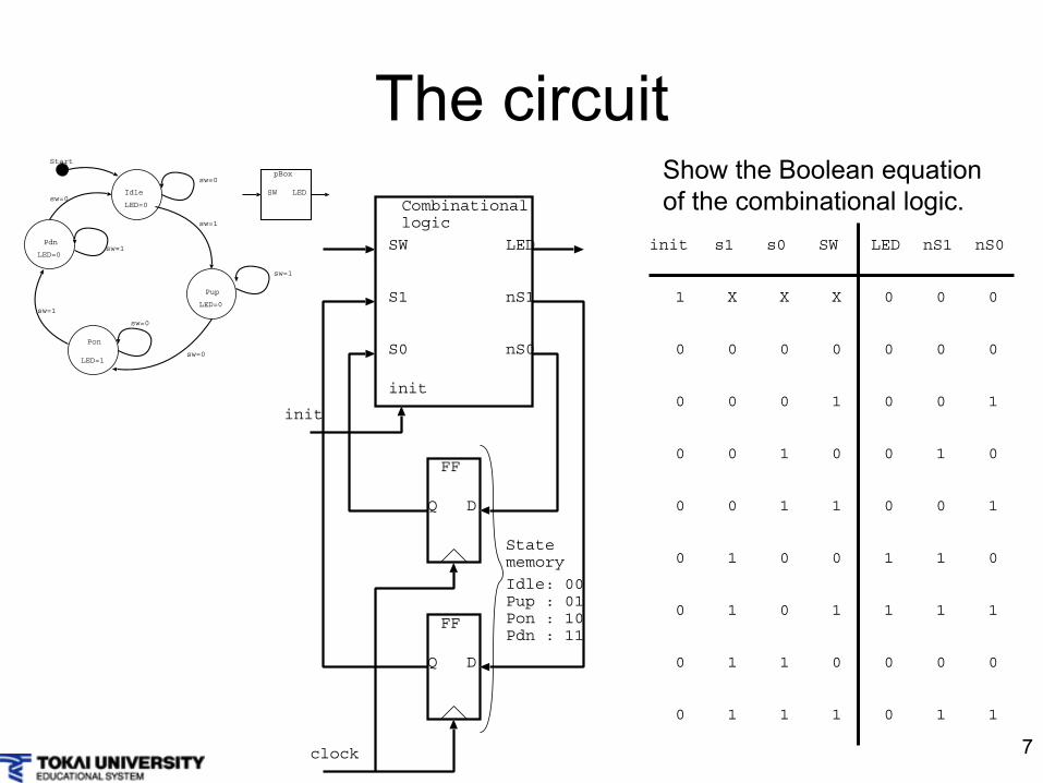
The circuit
SW LED
S1 nS1
S0 nS0
FF
FF
Combinationallogic
init
clock
init
Statememory
SWinit s1 s0 LED nS1 nS0
1 X X X 0 0 0
0 0 00 0 0 0
0 0 1
0 1 0
0 0 1
1 1 0
1 1 1
0 0 0
0 1 1
0 0 10
0 1 00
0 1 10
0 0 01
0 0 11
0 1 01
0 1 11
Idle: 00Pup : 01Pon : 10Pdn : 11
Q D
Q D
Start
Idle
Pup
Pon
sw=0
sw=1
sw=1
sw=0
Pdnsw=1
sw=0
sw=0
sw=1
SW LED
LED=0
LED=0
LED=1
LED=0
pBox Show the Boolean equation of the combinational logic.
8
Quiz
•
Draw the circuit for the crosswalk signal system.–
Draw the state machine
–
Designate the state assign–
Draw the circuit

1
Computer Architecture
Lecture 6State Machines -
2
2
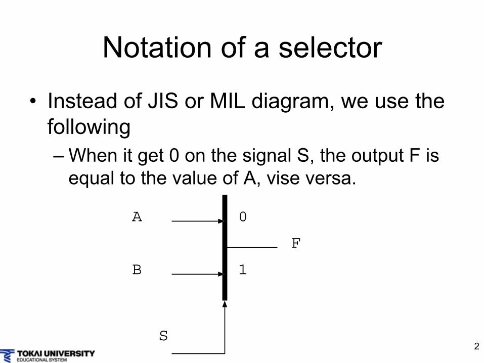
Notation of a selector
•
Instead of JIS or MIL diagram, we use the following–
When it get 0 on the signal S, the output F is equal to the value of A, vise versa.
A
B
S
0
1
F
3
Bus Notations
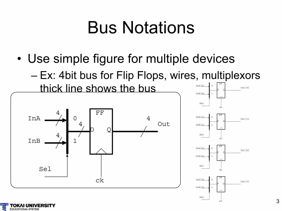
•
Use simple figure for multiple devices–
Ex: 4bit bus for Flip Flops, wires, multiplexors
thick line shows the bus
FF
QD4
4InAOut
InB
Sel
ck
0
1
4
4
FF
QDOut[0]
FF
QDOut[1]
FF
QDOut[2]
FF
QDOut[3]
InA[0]
InB[0]
Sel
0
1
InA[1]
InB[1]
Sel
0
1
InA[2]
InB[2]
Sel
0
1
InA[3]
InB[3]
Sel
0
1
ck
ck
ck
ck
4
BCD number
•
BCD stands for Binary Coded Decimal–
0 to 9 corresponds to 0000 to 1001
–
The numbers from 1010 to 1111 are illegal•
BCD number is often used for banking computations
5
BCD addition with binary adder
•
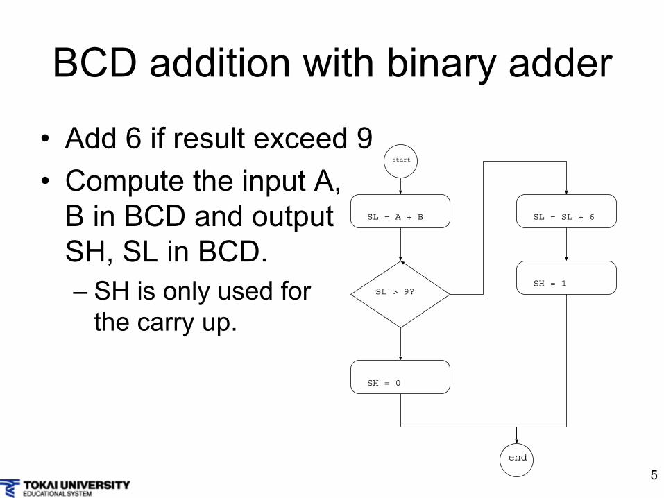
Add 6 if result exceed 9•
Compute the input A,
B in BCD and output SH, SL in BCD.
–
SH is only used for the carry up.
start
SL = A + B
SL > 9?
SL = SL + 6
SH = 1
SH = 0
end
6
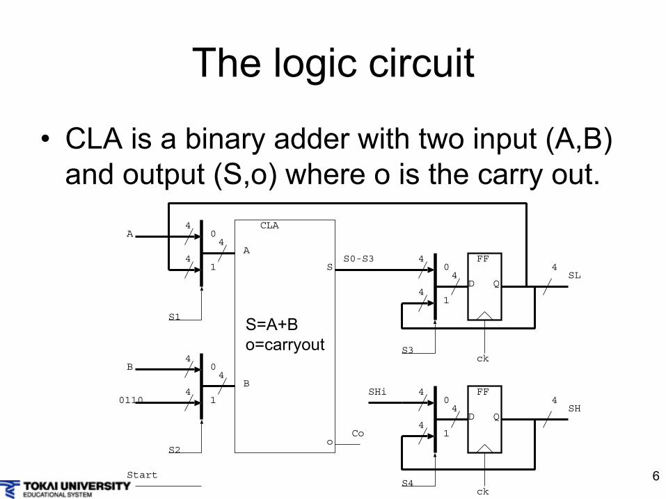
The logic circuit
•
CLA is a binary adder with two input (A,B) and output (S,o) where o is the carry out.
FF
QD
4
4
A
SL
ck
0
1
4
4
4B
0110
0
1
4
4 FF
QD
4SH
ck
40
1
4
4
40
1
4
4
CLA
A
B
S
o
S1
S2
S3
S4
Co
S0-S3
Start
SHi
S=A+Bo=carryout
7
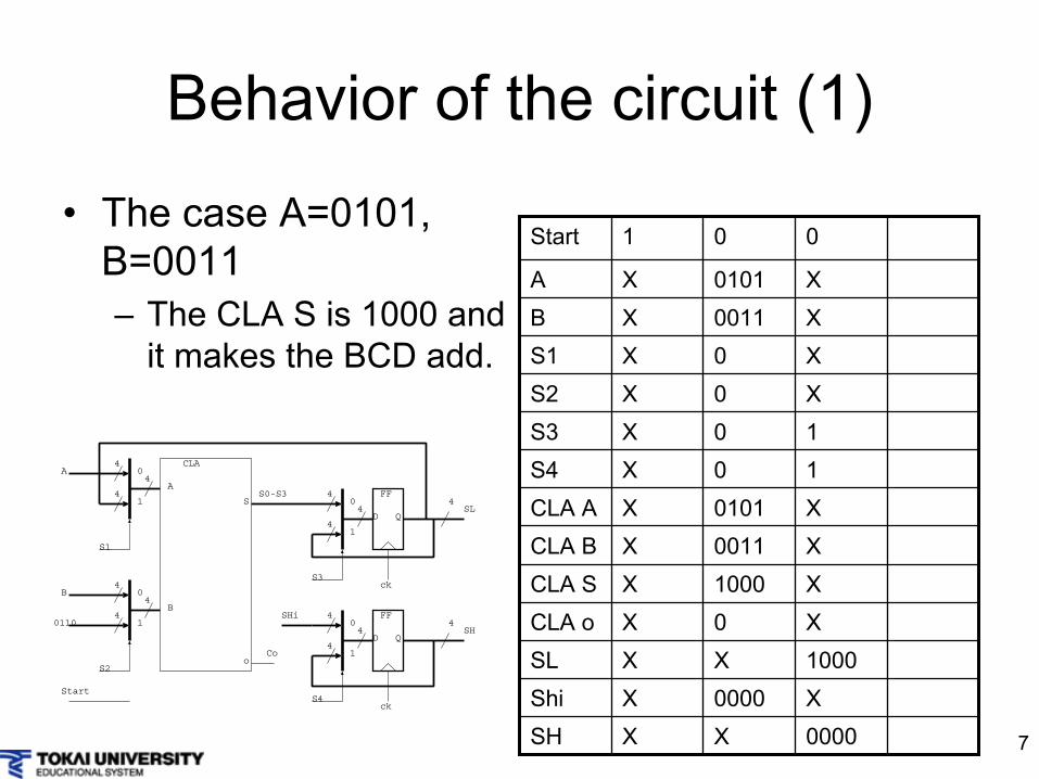
Behavior of the circuit (1)•
The case A=0101, B=0011–
The CLA S is 1000 and
it makes the BCD add.
Start 1 0 0
A X 0101 XB X 0011 XS1 X 0 XS2 X 0 XS3 X 0 1S4 X 0 1CLA A X 0101 XCLA B X 0011 XCLA S X 1000 XCLA o X 0 XSL X X 1000Shi X 0000 XSH X X 0000
FF
QD
4
4
A
SL
ck
0
1
4
4
4B
0110
0
1
4
4 FF
QD
4SH
ck
40
1
4
4
40
1
4
4
CLA
A
B
S
o
S1
S2
S3
S4
Co
S0-S3
Start
SHi
8
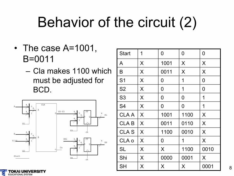
Behavior of the circuit (2)•
The case A=1001, B=0011–
Cla
makes 1100 which
must be adjusted for BCD.
Start 1 0 0 0
A X 1001 X XB X 0011 X XS1 X 0 1 0S2 X 0 1 0S3 X 0 0 1S4 X 0 0 1CLA A X 1001 1100 XCLA B X 0011 0110 XCLA S X 1100 0010 XCLA o X 0 1 XSL X X 1100 0010Shi X 0000 0001 XSH X X X 0001
FF
QD
4
4
A
SL
ck
0
1
4
4
4B
0110
0
1
4
4 FF
QD
4SH
ck
40
1
4
4
40
1
4
4
CLA
A
B
S
o
S1
S2
S3
S4
Co
S0-S3
Start
SHi
9
The state chart
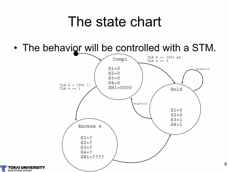
•
The behavior will be controlled with a STM.Start
start==1
start==0S1=0S2=0S3=0S4=0SHi=0000
Comp1
S1=0S2=0S3=1S4=1
CLA S <= 1001 &&CLA o == 0
HoldCLA S > 1001 ||CLA o == 1
Excess 6
S1=?S2=?S3=?S4=?SHi=????
10
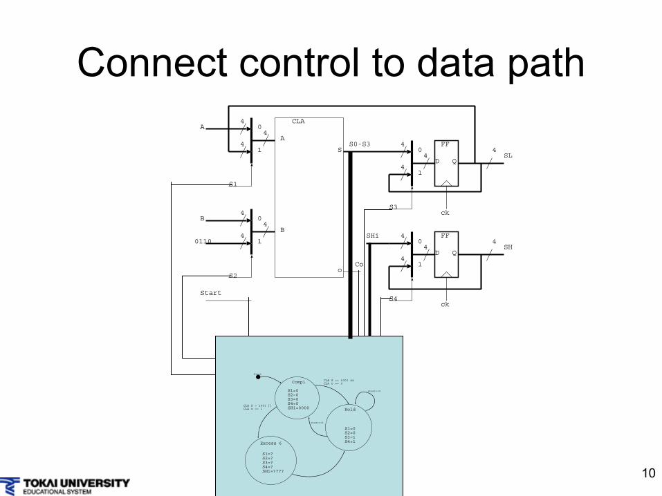
Connect control to data path
FF
QD
4
4
A
SL
ck
0
1
4
4
4B
0110
0
1
4
4 FF
QD
4SH
ck
40
1
4
4
40
1
4
4
CLA
A
B
S
o
S1
S2
S3
S4
Co
S0-S3
Start
SHi
Start
start==1
start==0S1=0S2=0S3=0S4=0SHi=0000
Comp1
S1=0S2=0S3=1S4=1
CLA S <= 1001 &&CLA o == 0
HoldCLA S > 1001 ||CLA o == 1
Excess 6
S1=?S2=?S3=?S4=?SHi=????
Start
start==1
start==0S1=0S2=0S3=0S4=0SHi=0000
Comp1
S1=0S2=0S3=1S4=1
CLA S <= 1001 &&CLA o == 0
HoldCLA S > 1001 ||CLA o == 1
Excess 6
S1=?S2=?S3=?S4=?SHi=????
11
Quiz
•
Complete the state chart•
Write the Boolean statement for “S > 1001 || o==1”
where S consists of S[0], S[1], S[2], S[3].•
Option [Draw the state machine of the BCD adder controller.]

1
Computer Architecture
Lecture 10Processor
2
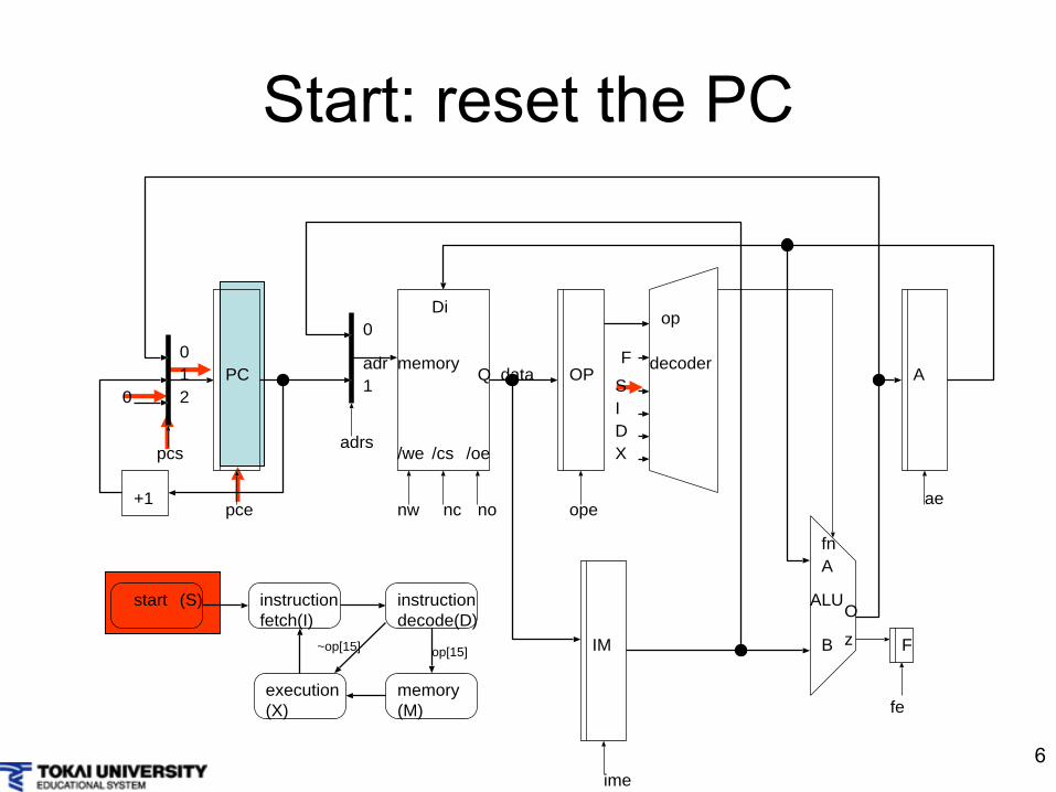
Processor•
Processor is a device which execute instructions in the memory.
•
We will divide the behavior into four steps.–
Start (S): We will reset the instruction pointer (PC)
–
Instruction Fetch (I): We will feed an address to the memory. And advance the pointer.
–
Instruction Decode (D): We will decode the instruction to make the execution.
–
Execution (X): We will execute the instruction
3
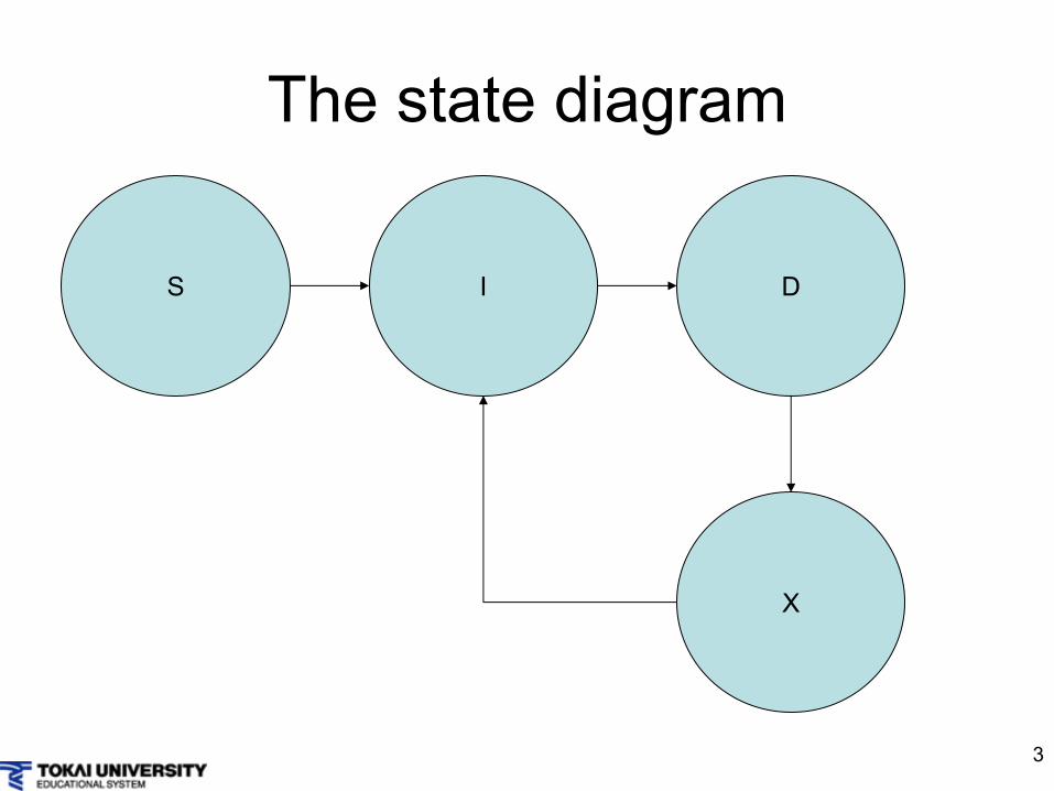
The state diagram
S I D
X
4
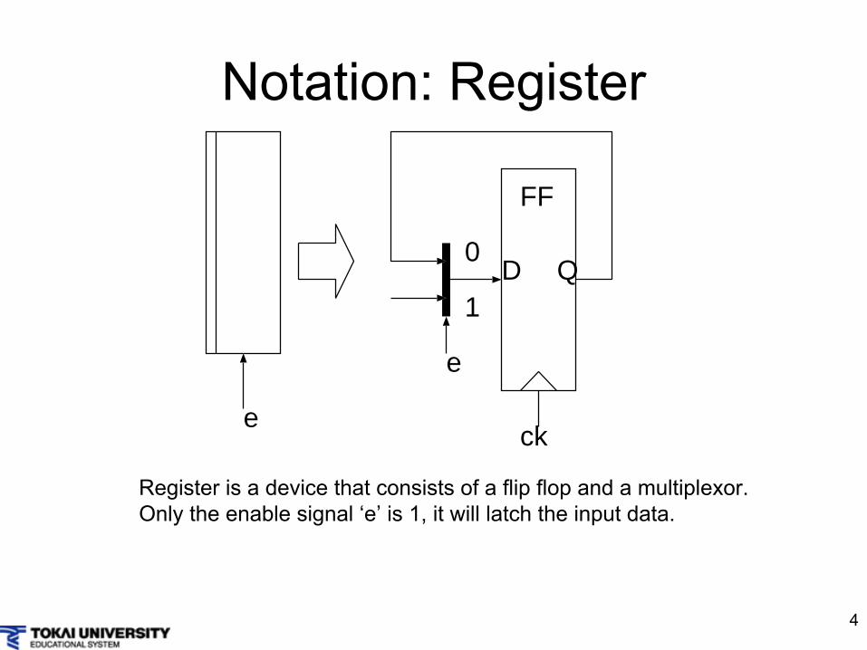
Notation: Register
FF
ck
D Q
e
e
1
0
Register is a device that consists of a flip flop and a multiplexor.Only the enable signal ‘e’
is 1, it will latch the input data.

5
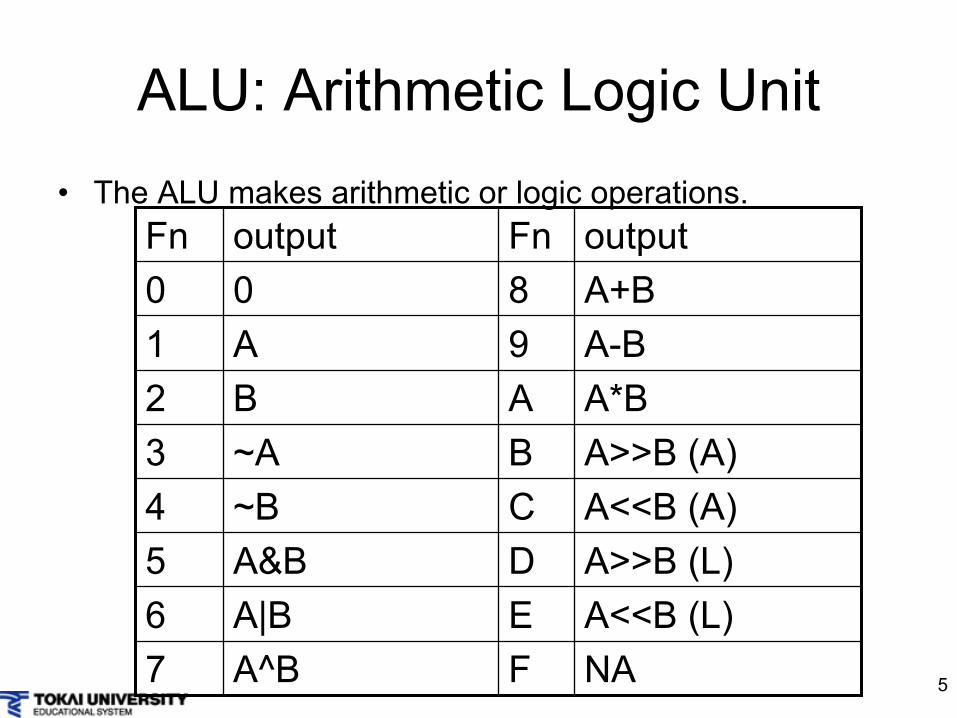
ALU: Arithmetic Logic Unit•
The ALU makes arithmetic or logic operations.
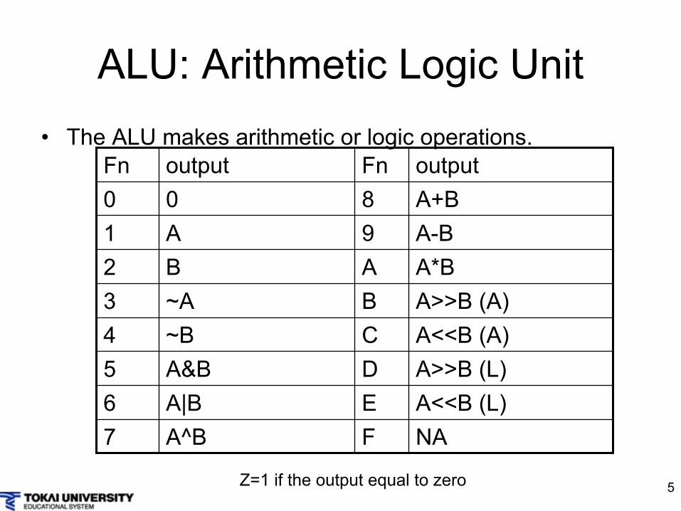
Fn output Fn output0 0 8 A+B1 A 9 A-B2 B A A*B3 ~A B A>>B (A)4 ~B C A<<B (A)5 A&B D A>>B (L)6 A|B E A<<B (L)7 A^B F NA
6
Block Diagram
PC OPmemoryadr
data
/cs /oe
+1
IM
Q
Di
/we
0A
opeae
ime
pce
pcs
nw nonc
adrs
ALU
fnA
B
00
11
2
decoder
start instructionfetch(I)
instructiondecode(D)
execution(X)
(S)
SIDX
7
Start: reset the PC
PC OPmemoryadr
data
/cs /oe
+1
IM
Q
Di
/we
0A
opeae
ime
pce
pcs
nw nonc
adrs
ALU
fnA
B
00
11
2
decoder
start instructionfetch(I)
instructiondecode(D)
execution(X)
(S)
SIDX

8
PC OPmemoryadr
data
/cs /oe
+1
IM
Q
Di
/we
0A
opeae
ime
pce
pcs
nw nonc
adrs
ALU
fnA
B
00
11
2
decoder
start instructionfetch(I)
instructiondecode(D)
execution(X)
(S)
SIDX
Instruction Fetch

9
PC OPmemoryadr
data
/cs /oe
+1
IM
Q
Di
/we
0A
opeae
ime
pce
pcs
nw nonc
adrs
ALU
fnA
B
00
11
2
decoder
start instructionfetch(I)
instructiondecode(D)
execution(X)
(S)
SIDX
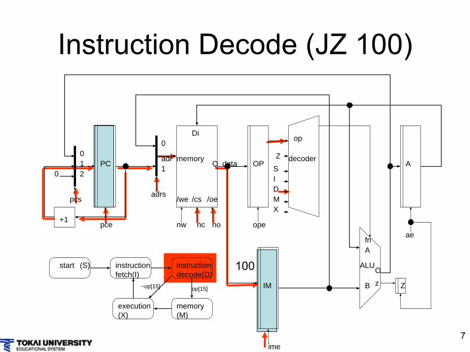
Instruction Decode

10
PC OPmemoryadr
data
/cs /oe
+1
IM
Q
Di
/we
0A
opeae
ime
pce
pcs
nw nonc
adrs
ALU
fnA
B
00
11
2
decoder
start instructionfetch(I)
instructiondecode(D)
execution(X)
(S)
SIDX
Execution (LDA #100)
11
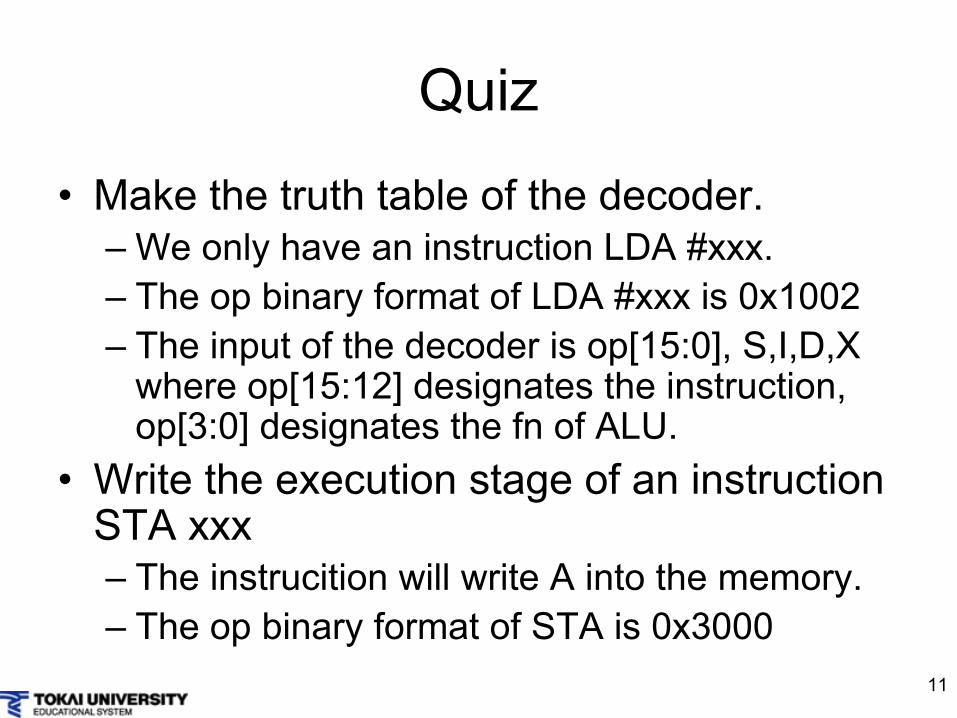
Quiz•
Make the truth table of the decoder.–
We only have an instruction LDA #xxx.
–
The op binary format of LDA #xxx is 0x1002–
The input of the decoder is op[15:0], S,I,D,X
where op[15:12] designates the instruction, op[3:0] designates the fn of ALU.
•
Write the execution stage of an instruction STA xxx–
The instrucition
will write A into the memory.
–
The op binary format of STA is 0x3000
1
Computer Architecture
Lecture 11Processor-2
Add instructions
2
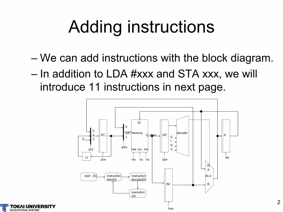
Adding instructions–
We can add instructions with the block diagram.
–
In addition to LDA #xxx and STA xxx, we will introduce 11 instructions in next page.
PC OPmemoryadr
data
/cs /oe
+1
IM
Q
Di
/we
0A
opeae
ime
pce
pcs
nw nonc
adrs
ALU
fnA
B
00
11
2
decoder
start instructionfetch(I)
instructiondecode(D)
execution(X)
(S)
SIDX
3
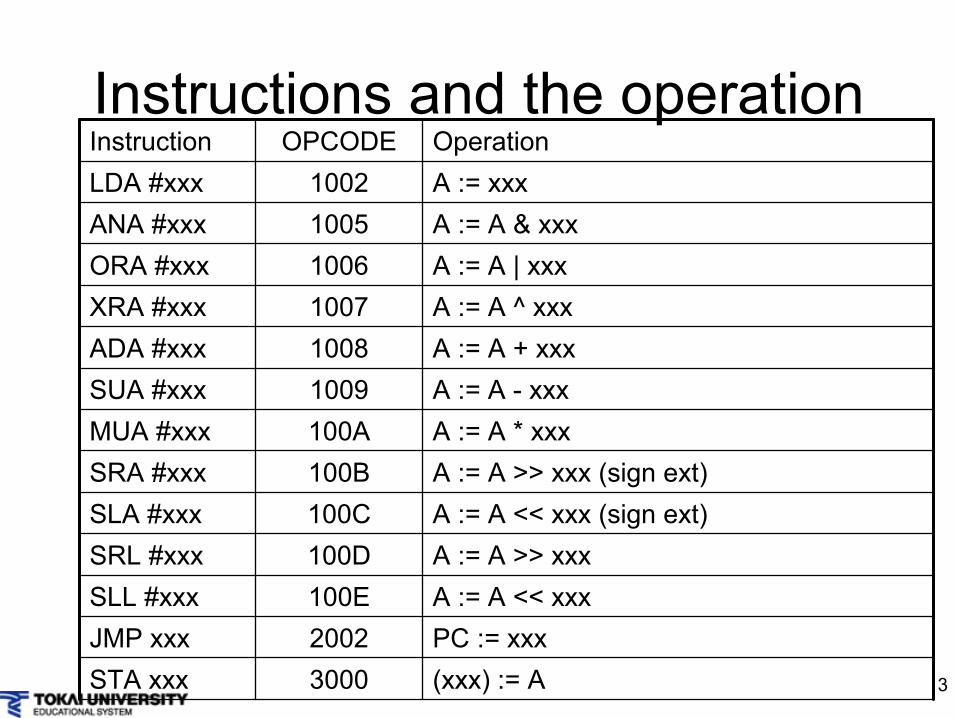
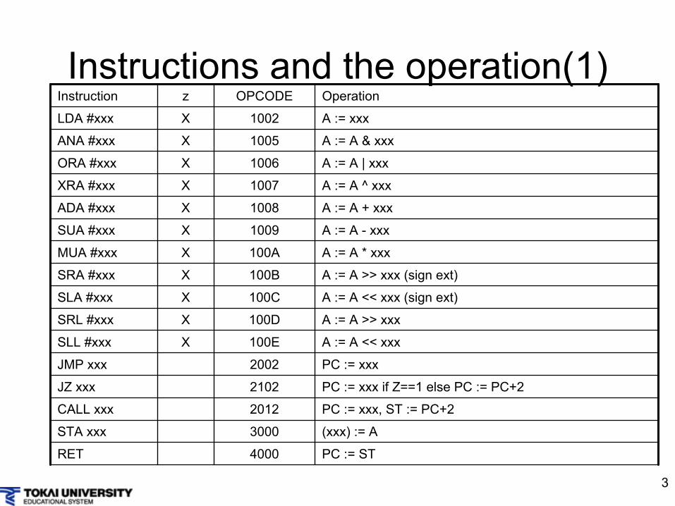
Instructions and the operationInstruction OPCODE OperationLDA #xxx 1002 A := xxxANA #xxx 1005 A := A & xxxORA #xxx 1006 A := A | xxxXRA #xxx 1007 A := A ^ xxxADA #xxx 1008 A := A + xxxSUA #xxx 1009 A := A -
xxxMUA #xxx 100A A := A * xxxSRA #xxx 100B A := A >> xxx (sign ext)SLA #xxx 100C A := A << xxx (sign ext)SRL #xxx 100D A := A >> xxxSLL #xxx 100E A := A << xxxJMP xxx 2002 PC := xxxSTA xxx 3000 (xxx) := A

4
ALU: Arithmetic Logic Unit•
The ALU makes arithmetic or logic operations.
Fn output Fn output0 0 8 A+B1 A 9 A-B2 B A A*B3 ~A B A>>B (A)4 ~B C A<<B (A)5 A&B D A>>B (L)6 A|B E A<<B (L)7 A^B F NA

5
Start: reset the PC
PC OPmemoryadr
data
/cs /oe
+1
IM
Q
Di
/we
0A
opeae
ime
pce
pcs
nw nonc
adrs
ALU
fnA
B
00
11
2
decoder
start instructionfetch(I)
instructiondecode(D)
execution(X)
(S)
SIDX
6
PC OPmemoryadr
data
/cs /oe
+1
IM
Q
Di
/we
0A
opeae
ime
pce
pcs
nw nonc
adrs
ALU
fnA
B
00
11
2
decoder
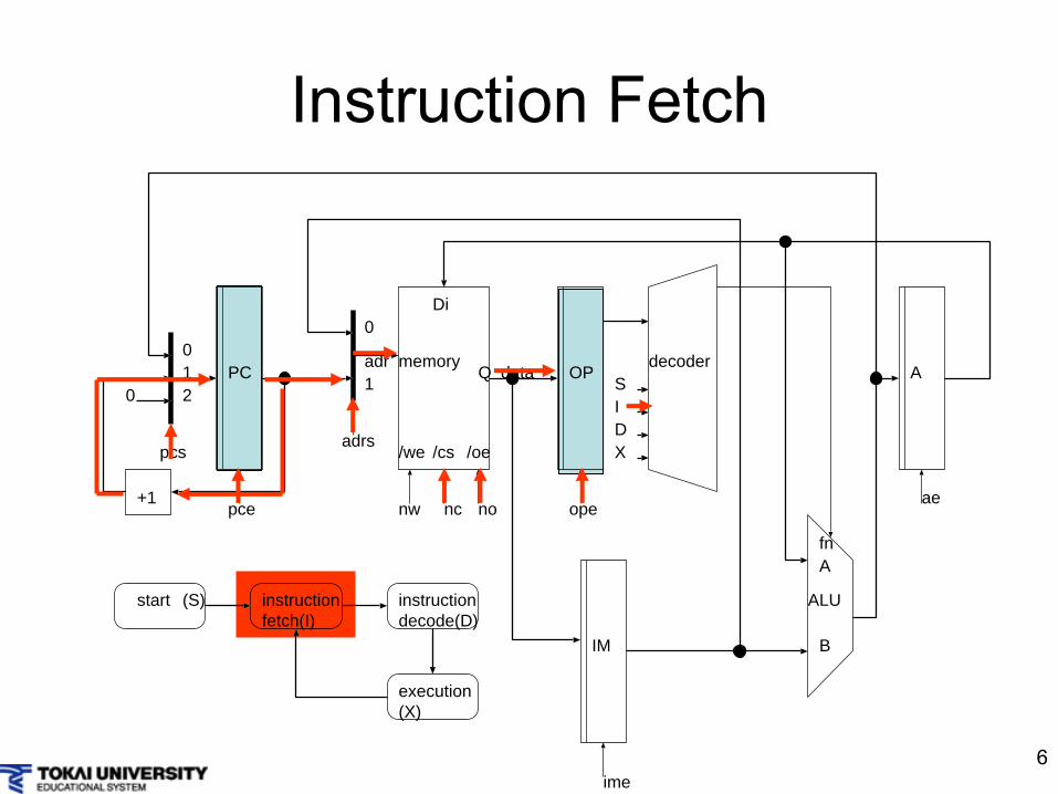
start instructionfetch(I)
instructiondecode(D)
execution(X)
(S)
SIDX
Instruction Fetch
7
PC OPmemoryadr
data
/cs /oe
+1
IM
Q
Di
/we
0A
opeae
ime
pce
pcs
nw nonc
adrs
ALU
fnA
B
00
11
2
decoder
start instructionfetch(I)
instructiondecode(D)
execution(X)
(S)
SIDX
Instruction Decode
8
PC OPmemoryadr
data
/cs /oe
+1
IM
Q
Di
/we
0A
opeae
ime
pce
pcs
nw nonc
adrs
ALU
fnA
B
00
11
2
decoder
start instructionfetch(I)
instructiondecode(D)
execution(X)
(S)
SIDX
Execution (LDA #100)
9
Truth table of the decoder
S I D X OP
pcs
pce
adrs
ope
ime
ae nw nc no fn
1 0 0 0 *
0 1 0 0 *
0 0 1 0
0 0 0 1
10
Quiz
•
Make the truth table of the decoder.–
At first you can start with separate decoders for each instruction. (not mandatory)
–
Then you can merge the decoders into one simple decoder.
•
Write the modification on the block diagram to support an instruction : LDA (xxx)
that is to load the content of the memory at the address xxx.
1
Computer Architecture
Lecture 12Processor-3
Add instructions
2
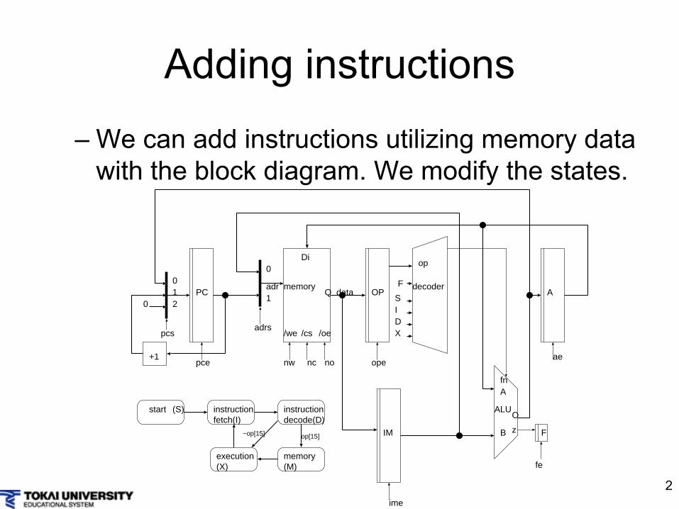
Adding instructions–
We can add instructions utilizing memory data with the block diagram. We modify the states.
PC OPmemoryadr
data
/cs /oe
+1
IM
Q
Di
/we
0A
opeae
ime
pce
pcs
nw nonc
adrs
ALU
fnA
B
00
11
2
decoder
start instructionfetch(I)
instructiondecode(D)
execution(X)
(S)
SIDX
op
O
z
fe
F
F
memory(M)
op[15]~op[15]
3
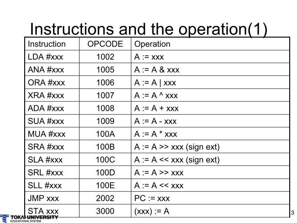
Instructions and the operation(1)Instruction OPCODE OperationLDA #xxx 1002 A := xxxANA #xxx 1005 A := A & xxxORA #xxx 1006 A := A | xxxXRA #xxx 1007 A := A ^ xxxADA #xxx 1008 A := A + xxxSUA #xxx 1009 A := A -
xxxMUA #xxx 100A A := A * xxxSRA #xxx 100B A := A >> xxx (sign ext)SLA #xxx 100C A := A << xxx (sign ext)SRL #xxx 100D A := A >> xxxSLL #xxx 100E A := A << xxxJMP xxx 2002 PC := xxxSTA xxx 3000 (xxx) := A
4
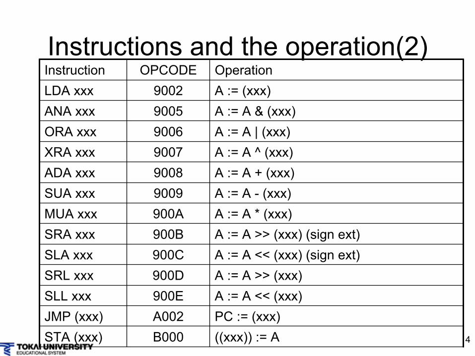
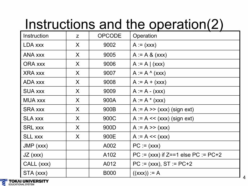
Instructions and the operation(2)Instruction OPCODE OperationLDA xxx 9002 A := (xxx)ANA xxx 9005 A := A & (xxx)ORA xxx 9006 A := A | (xxx)XRA xxx 9007 A := A ^ (xxx)ADA xxx 9008 A := A + (xxx)SUA xxx 9009 A := A -
(xxx)MUA xxx 900A A := A * (xxx)SRA xxx 900B A := A >> (xxx) (sign ext)SLA xxx 900C A := A << (xxx) (sign ext)SRL xxx 900D A := A >> (xxx)SLL xxx 900E A := A << (xxx)JMP (xxx) A002 PC := (xxx)STA (xxx) B000 ((xxx)) := A
5
ALU: Arithmetic Logic Unit•
The ALU makes arithmetic or logic operations.
Fn output Fn output0 0 8 A+B1 A 9 A-B2 B A A*B3 ~A B A>>B (A)4 ~B C A<<B (A)5 A&B D A>>B (L)6 A|B E A<<B (L)7 A^B F NA
6
Start: reset the PC
PC OPmemoryadr
data
/cs /oe
+1
IM
Q
Di
/we
0A
opeae
ime
pce
pcs
nw nonc
adrs
ALU
fnA
B
00
11
2
decoder
start instructionfetch(I)
instructiondecode(D)
execution(X)
(S)
SIDX
op
O
z
fe
F
F
memory(M)
op[15]~op[15]
7
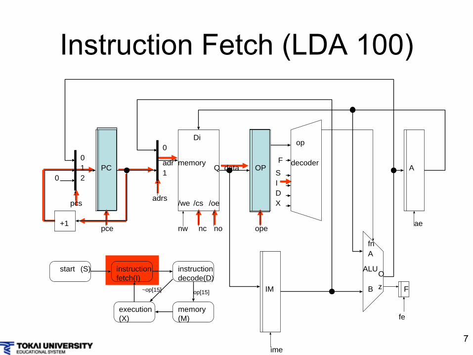
Instruction Fetch (LDA 100)
PC OPmemoryadr
data
/cs /oe
+1
IM
Q
Di
/we
0A
opeae
ime
pce
pcs
nw nonc
adrs
ALU
fnA
B
00
11
2
decoder
start instructionfetch(I)
instructiondecode(D)
execution(X)
(S)
SIDX
op
O
z
fe
F
F
memory(M)
op[15]~op[15]
8
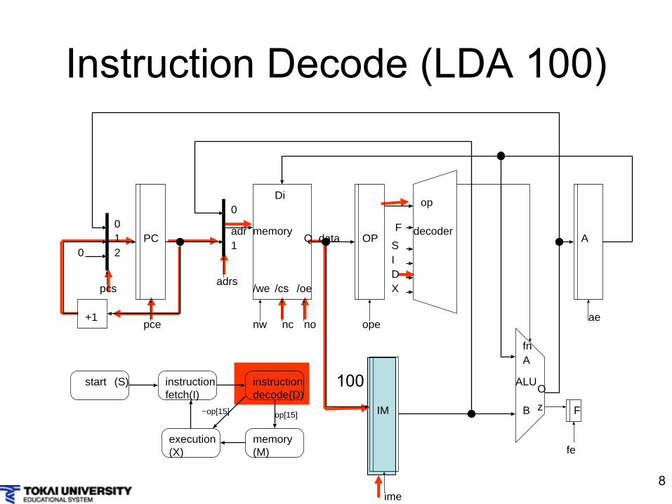
Instruction Decode (LDA 100)
PC OPmemoryadr
data
/cs /oe
+1
IM
Q
Di
/we
0A
opeae
ime
pce
pcs
nw nonc
adrs
ALU
fnA
B
00
11
2
decoder
start instructionfetch(I)
instructiondecode(D)
execution(X)
(S)
SIDX
op
O
z
fe
F
F
memory(M)
op[15]~op[15]
100
9
PC OPmemoryadr
data
/cs /oe
+1
IM
Q
Di
/we
0A
opeae
ime
pce
pcs
nw nonc
adrs
ALU
fnA
B
00
11
2
decoder
start instructionfetch(I)
instructiondecode(D)
execution(X)
(S)
SIDX
op
O
z
fe
F
F
memory(M)
op[15]~op[15]
Memory (LDA 100)
100(100)
10
Execution (LDA 100)
PC OPmemoryadr
data
/cs /oe
+1
IM
Q
Di
/we
0A
opeae
ime
pce
pcs
nw nonc
adrs
ALU
fnA
B
00
11
2
decoder
start instructionfetch(I)
instructiondecode(D)
execution(X)
(S)
SIDX
op
O
z
fe
F
F
memory(M)
op[15]~op[15](100)

11
Truth table of the decoder
S I D X OP
pcs
pce
adrs
ope
ime
ae nw nc no fn
1 0 0 0 *
0 1 0 0 *
0 0 1 0
0 0 0 1
M
0
0
0
0
0 0 0 01
12
Quiz•
Make the truth table of the decoder.
•
Write the behavior of the CPU which runs from address 0 on the following table.
address instruction behavior
0 LDA #10
2 STA 100
4 LDA # -1
6 ADA 100
8 STA 100
10 SUA #50
12 ADA 100
1
Computer Architecture
Lecture 13Processor-4
instructions for conditional branch
2
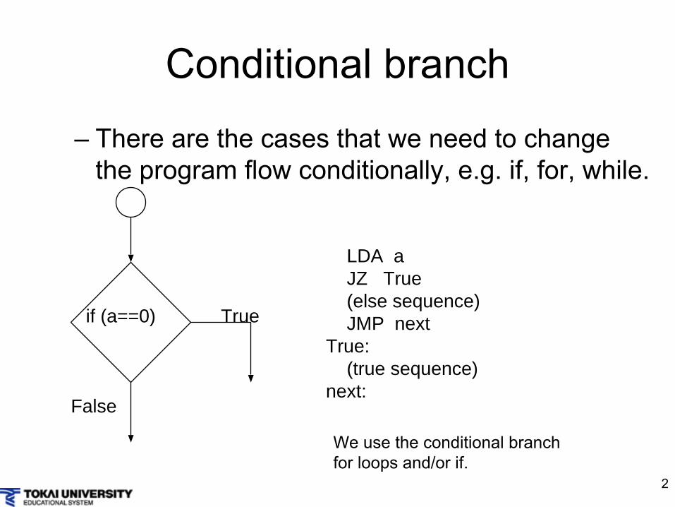
Conditional branch–
There are the cases that we need to change the program flow conditionally, e.g. if, for, while.
We use the conditional branch for loops and/or if.
if (a==0) True
False
LDA a JZ True (else sequence) JMP nextTrue: (true sequence)next:
3
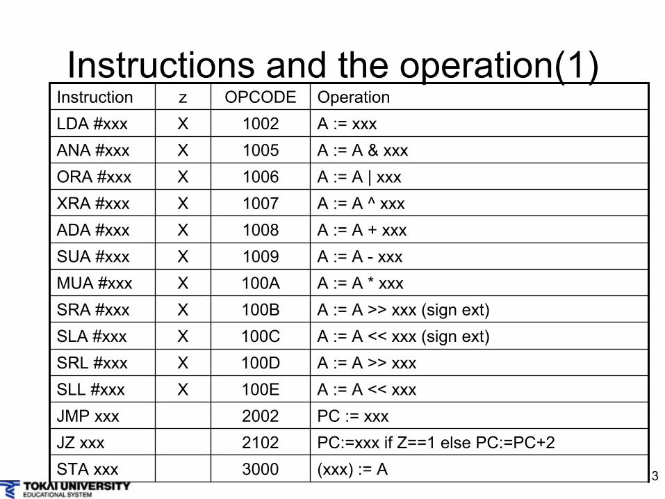
Instructions and the operation(1)Instruction z OPCODE OperationLDA #xxx X 1002 A := xxxANA #xxx X 1005 A := A & xxxORA #xxx X 1006 A := A | xxxXRA #xxx X 1007 A := A ^ xxxADA #xxx X 1008 A := A + xxxSUA #xxx X 1009 A := A -
xxxMUA #xxx X 100A A := A * xxxSRA #xxx X 100B A := A >> xxx (sign ext)SLA #xxx X 100C A := A << xxx (sign ext)SRL #xxx X 100D A := A >> xxxSLL #xxx X 100E A := A << xxxJMP xxx 2002 PC := xxxJZ xxx 2102 PC:=xxx if Z==1 else PC:=PC+2STA xxx 3000 (xxx) := A
4
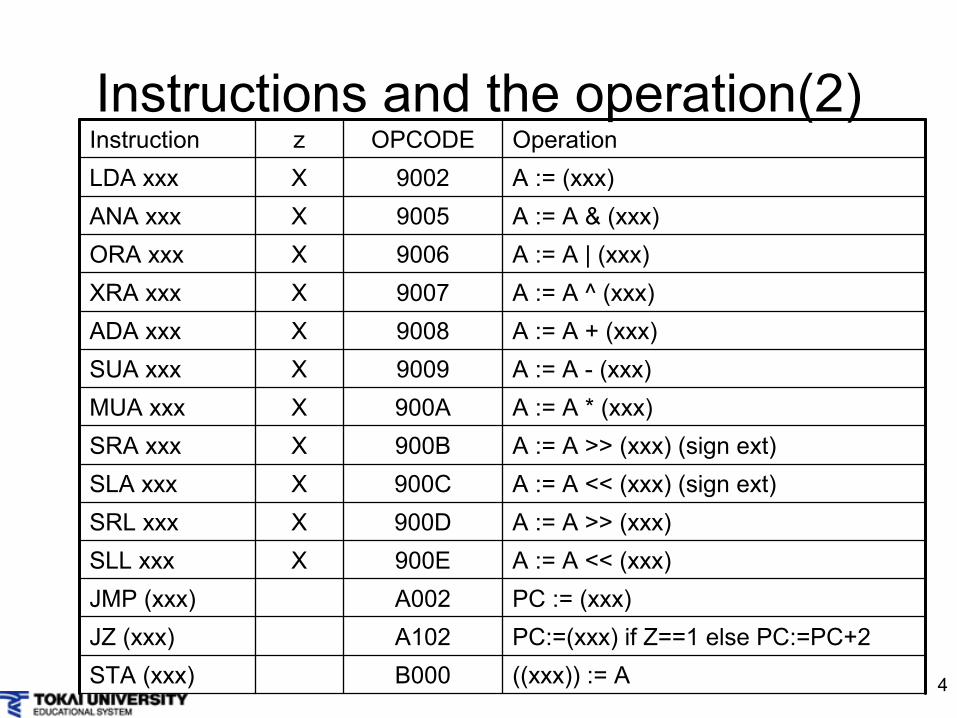
Instructions and the operation(2)Instruction z OPCODE OperationLDA xxx X 9002 A := (xxx)ANA xxx X 9005 A := A & (xxx)ORA xxx X 9006 A := A | (xxx)XRA xxx X 9007 A := A ^ (xxx)ADA xxx X 9008 A := A + (xxx)SUA xxx X 9009 A := A -
(xxx)MUA xxx X 900A A := A * (xxx)SRA xxx X 900B A := A >> (xxx) (sign ext)SLA xxx X 900C A := A << (xxx) (sign ext)SRL xxx X 900D A := A >> (xxx)SLL xxx X 900E A := A << (xxx)JMP (xxx) A002 PC := (xxx)JZ (xxx) A102 PC:=(xxx) if Z==1 else PC:=PC+2STA (xxx) B000 ((xxx)) := A

5
ALU: Arithmetic Logic Unit•
The ALU makes arithmetic or logic operations.
Fn output Fn output0 0 8 A+B1 A 9 A-B2 B A A*B3 ~A B A>>B (A)4 ~B C A<<B (A)5 A&B D A>>B (L)6 A|B E A<<B (L)7 A^B F NA
Z=1 if the output equal to zero
6
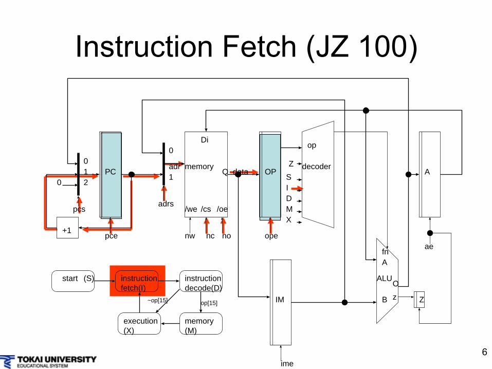
Instruction Fetch (JZ 100)
PC OPmemoryadr
data
/cs /oe
+1
IM
Q
Di
/we
0A
opeae
ime
pce
pcs
nw nonc
adrs
ALU
fnA
B
00
11
2
decoder
start instructionfetch(I)
instructiondecode(D)
execution(X)
(S)
SIDM
op
O
z Z
Z
memory(M)
op[15]~op[15]
X
7
Instruction Decode (JZ 100)
100
PC OPmemoryadr
data
/cs /oe
+1
IM
Q
Di
/we
0A
opeae
ime
pce
pcs
nw nonc
adrs
ALU
fnA
B
00
11
2
decoder
start instructionfetch(I)
instructiondecode(D)
execution(X)
(S)
SIDM
op
O
z Z
Z
memory(M)
op[15]~op[15]
X
8
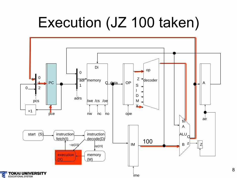
Execution (JZ 100 taken)
100
PC OPmemoryadr
data
/cs /oe
+1
IM
Q
Di
/we
0A
opeae
ime
pce
pcs
nw nonc
adrs
ALU
fnA
B
00
11
2
decoder
start instructionfetch(I)
instructiondecode(D)
execution(X)
(S)
SIDM
op
O
z Z
Z
memory(M)
op[15]~op[15]
X
9
PC OPmemoryadr
data
/cs /oe
+1
IM
Q
Di
/we
0A
opeae
ime
pce
pcs
nw nonc
adrs
ALU
fnA
B
00
11
2
decoder
start instructionfetch(I)
instructiondecode(D)
execution(X)
(S)
SIDM
op
O
z Z
Z
memory(M)
op[15]~op[15]
X
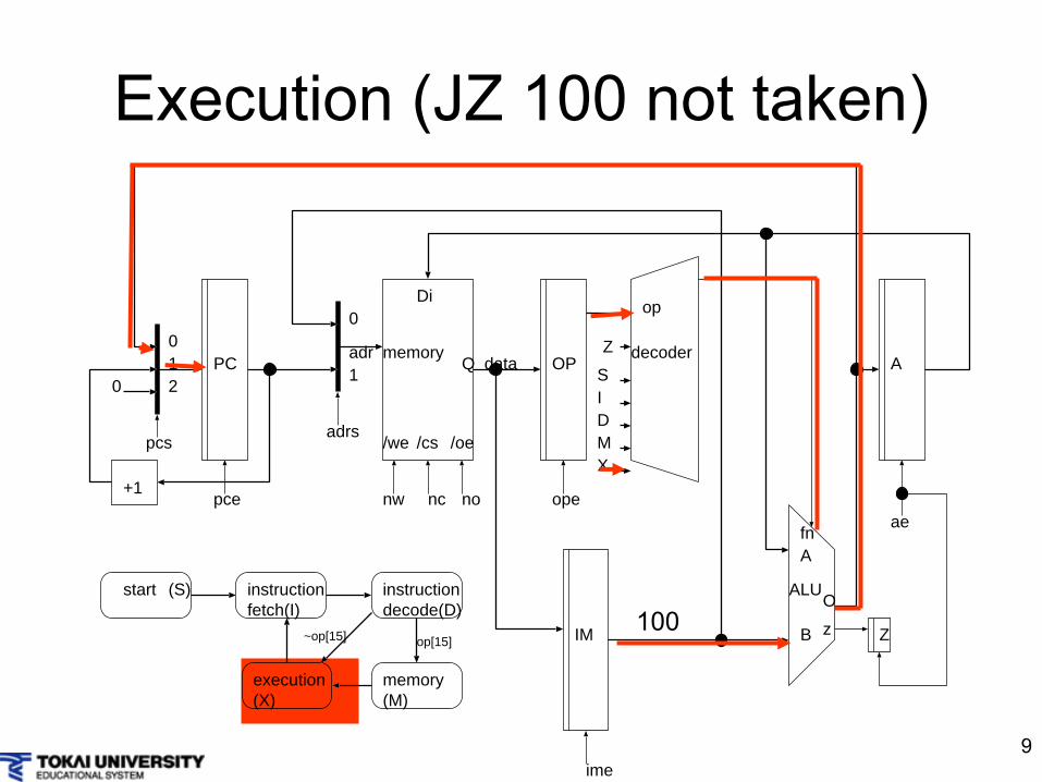
Execution (JZ 100 not taken)
100
10
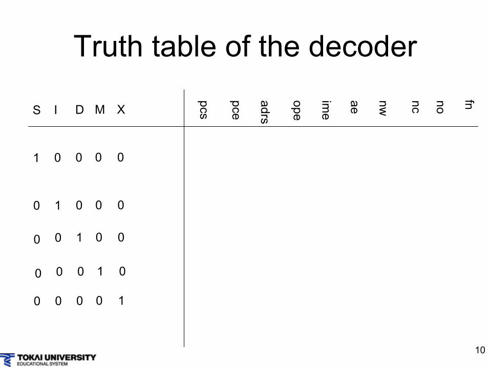
Truth table of the decoder
S I D X
pcs
pce
adrs
ope
ime
ae nw nc no fn
1 0 0 0
0 1 0 0
0 0 1 0
0 0 0 1
M
0
0
0
0
0 0 0 01
11
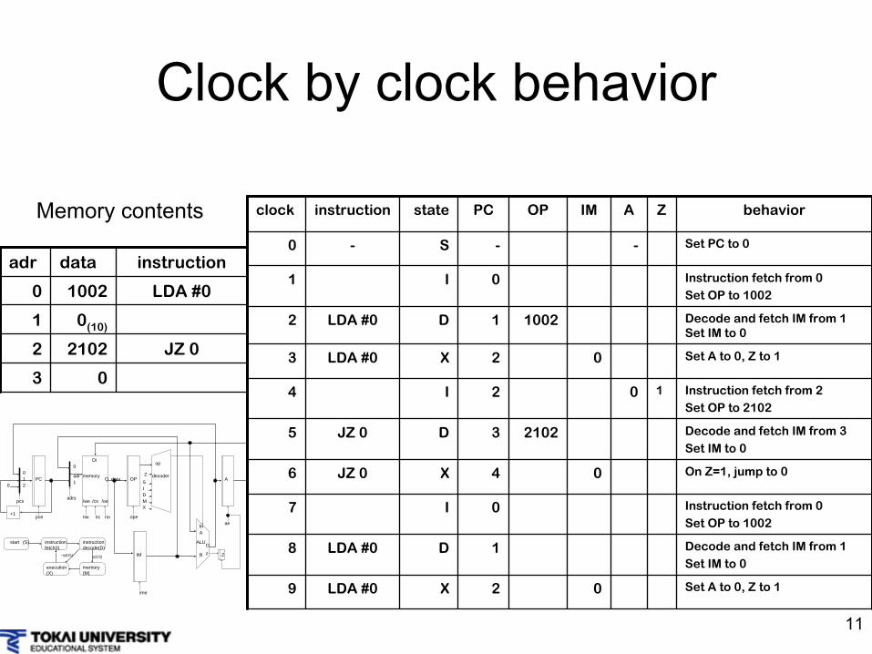
Clock by clock behavior
clock instruction state PC OP IM A Z behavior
0 - S - - Set PC to 0
1 I 0 Instruction fetch from 0Set OP to 1002
2 LDA #0 D 1 1002 Decode and fetch IM from 1
Set IM to 0
3 LDA #0 X 2 0 Set A to 0, Z to 1
4 I 2 0 1 Instruction fetch from 2Set OP to 2102
5 JZ 0 D 3 2102 Decode and fetch IM from 3Set IM to 0
6 JZ 0 X 4 0 On Z=1, jump to 0
7 I 0 Instruction fetch from 0Set OP to 1002
8 LDA #0 D 1 Decode and fetch IM from 1Set IM to 0
9 LDA #0 X 2 0 Set A to 0, Z to 1
adr data instruction
0 1002 LDA #0
1 0(10)
2 2102 JZ 0
3 0
Memory contents
PC OPmemoryadr
data
/cs /oe
+1
IM
Q
Di
/we
0A
opeae
ime
pce
pcs
nw nonc
adrs
ALU
fnA
B
00
11
2
decoder
start instructionfetch(I)
instructiondecode(D)
execution(X)
(S)
SIDM
op
O
z Z
Z
memory(M)
op[15]~op[15]
X
12
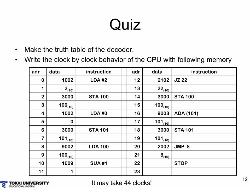
Quiz•
Make the truth table of the decoder.•
Write the clock by clock behavior of the CPU with following memoryadr data instruction adr data instruction
0 1002 LDA #2 12 2102 JZ 22
1 2(10) 13 22(10)
2 3000 STA 100 14 3000 STA 100
3 100(10) 15 100(10)
4 1002 LDA #0 16 9008 ADA (101)
5 0 17 101(10)
6 3000 STA 101 18 3000 STA 101
7 101(10) 19 101(10)
8 9002 LDA 100 20 2002 JMP 8
9 100(10) 21 8(10)
10 1009 SUA #1 22 STOP
11 1 23
It may take 44 clocks!
1
Computer Architecture
Lecture 14Processor-5
instructions for call/return
2
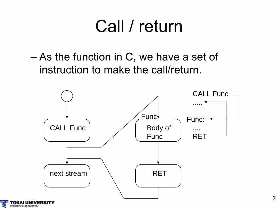
Call / return–
As the function in C, we have a set of instruction to make the call/return.
CALL Func .....
Func: .... RET
CALL Func
RET
Func
Body ofFunc
next stream
3
Instructions and the operation(1)Instruction z OPCODE Operation
LDA #xxx X 1002 A := xxxANA #xxx X 1005 A := A & xxx
ORA #xxx X 1006 A := A | xxx
XRA #xxx X 1007 A := A ^ xxx
ADA #xxx X 1008 A := A + xxx
SUA #xxx X 1009 A := A -
xxx
MUA #xxx X 100A A := A * xxx
SRA #xxx X 100B A := A >> xxx (sign ext)
SLA #xxx X 100C A := A << xxx (sign ext)
SRL #xxx X 100D A := A >> xxx
SLL #xxx X 100E A := A << xxx
JMP xxx 2002 PC := xxx
JZ xxx 2102 PC := xxx if Z==1 else PC := PC+2CALL xxx 2012 PC := xxx, ST := PC+2
STA xxx 3000 (xxx) := A
RET 4000 PC := ST
4
Instructions and the operation(2)Instruction z OPCODE OperationLDA xxx X 9002 A := (xxx)
ANA xxx X 9005 A := A & (xxx)ORA xxx X 9006 A := A | (xxx)XRA xxx X 9007 A := A ^ (xxx)ADA xxx X 9008 A := A + (xxx)SUA xxx X 9009 A := A -
(xxx)MUA xxx X 900A A := A * (xxx)SRA xxx X 900B A := A >> (xxx) (sign ext)SLA xxx X 900C A := A << (xxx) (sign ext)SRL xxx X 900D A := A >> (xxx)SLL xxx X 900E A := A << (xxx)JMP (xxx) A002 PC := (xxx)JZ (xxx) A102 PC := (xxx) if Z==1 else PC := PC+2CALL (xxx) A012 PC := (xxx), ST := PC+2STA (xxx) B000 ((xxx)) := A
5
ALU: Arithmetic Logic Unit•
The ALU makes arithmetic or logic operations.
Fn output Fn output0 0 8 A+B1 A 9 A-B2 B A A*B3 ~A B A>>B (A)4 ~B C A<<B (A)5 A&B D A>>B (L)6 A|B E A<<B (L)7 A^B F NA
Z=1 if the output equal to zero
6
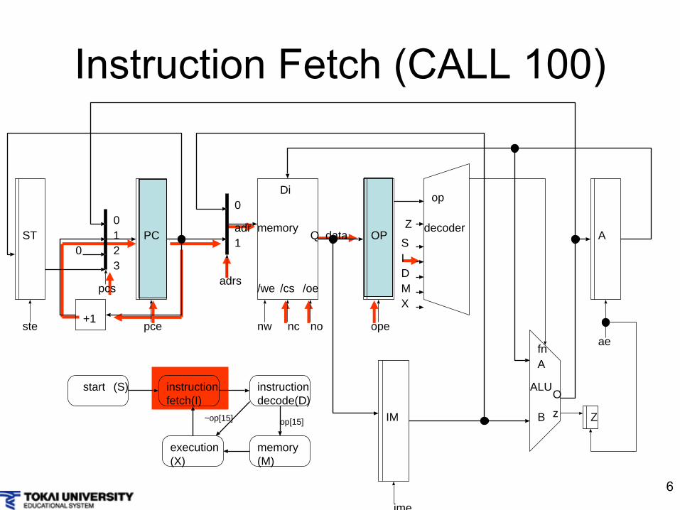
Instruction Fetch (CALL 100)
PC OPmemoryadr
data
/cs /oe
+1
IM
Q
Di
/we
0A
opeae
ime
pce
pcs
nw nonc
adrs
ALU
fnA
B
00
11
2
decoder
start instructionfetch(I)
instructiondecode(D)
execution(X)
(S)
SIDM
op
O
z Z
Z
memory(M)
op[15]~op[15]
X
ST
ste
3
7
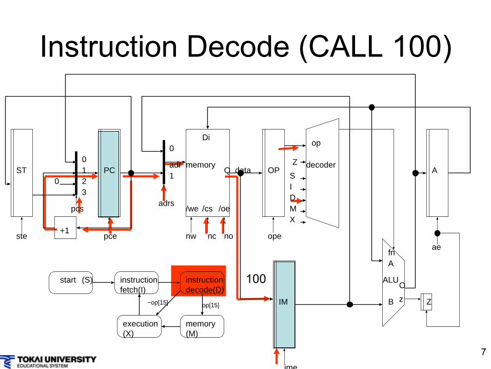
Instruction Decode (CALL 100)
100
PC OPmemoryadr
data
/cs /oe
+1
IM
Q
Di
/we
0A
opeae
ime
pce
pcs
nw nonc
adrs
ALU
fnA
B
00
11
2
decoder
start instructionfetch(I)
instructiondecode(D)
execution(X)
(S)
SIDM
op
O
z Z
Z
memory(M)
op[15]~op[15]
X
ST
ste
3
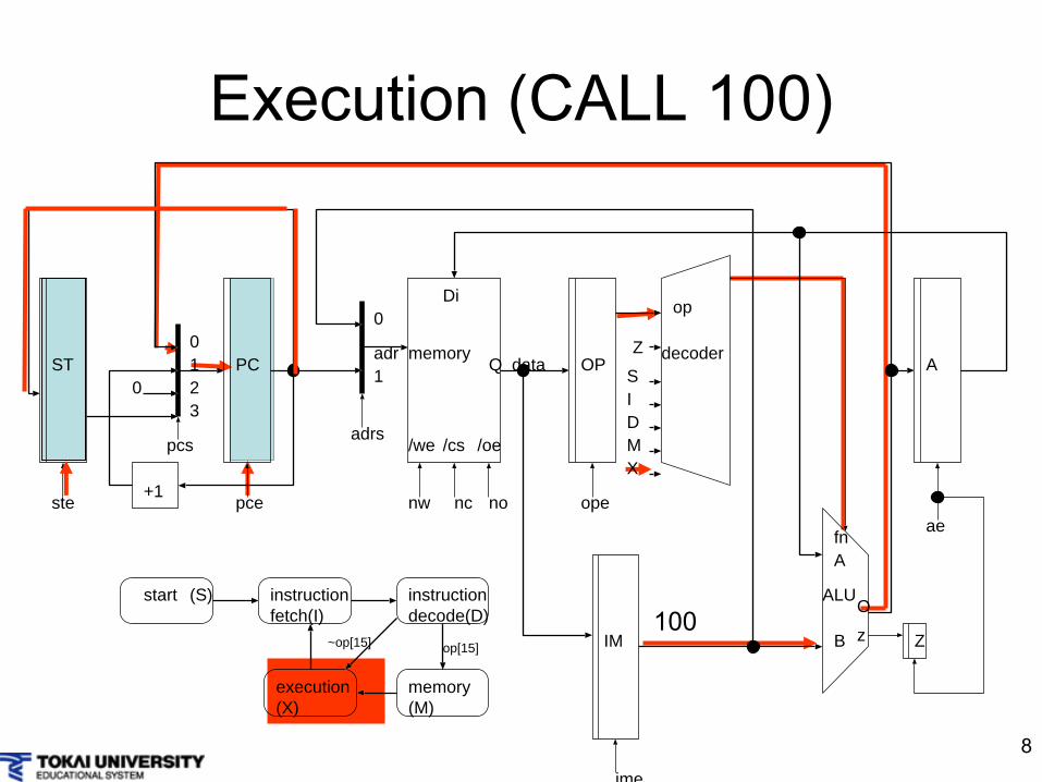
8
Execution (CALL 100)
100
PC OPmemoryadr
data
/cs /oe
+1
IM
Q
Di
/we
0A
opeae
ime
pce
pcs
nw nonc
adrs
ALU
fnA
B
00
11
2
decoder
start instructionfetch(I)
instructiondecode(D)
execution(X)
(S)
SIDM
op
O
z Z
Z
memory(M)
op[15]~op[15]
X
ST
ste
3
9
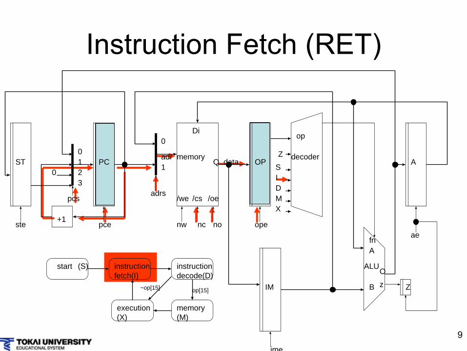
Instruction Fetch (RET)
PC OPmemoryadr
data
/cs /oe
+1
IM
Q
Di
/we
0A
opeae
ime
pce
pcs
nw nonc
adrs
ALU
fnA
B
00
11
2
decoder
start instructionfetch(I)
instructiondecode(D)
execution(X)
(S)
SIDM
op
O
z Z
Z
memory(M)
op[15]~op[15]
X
ST
ste
3
10
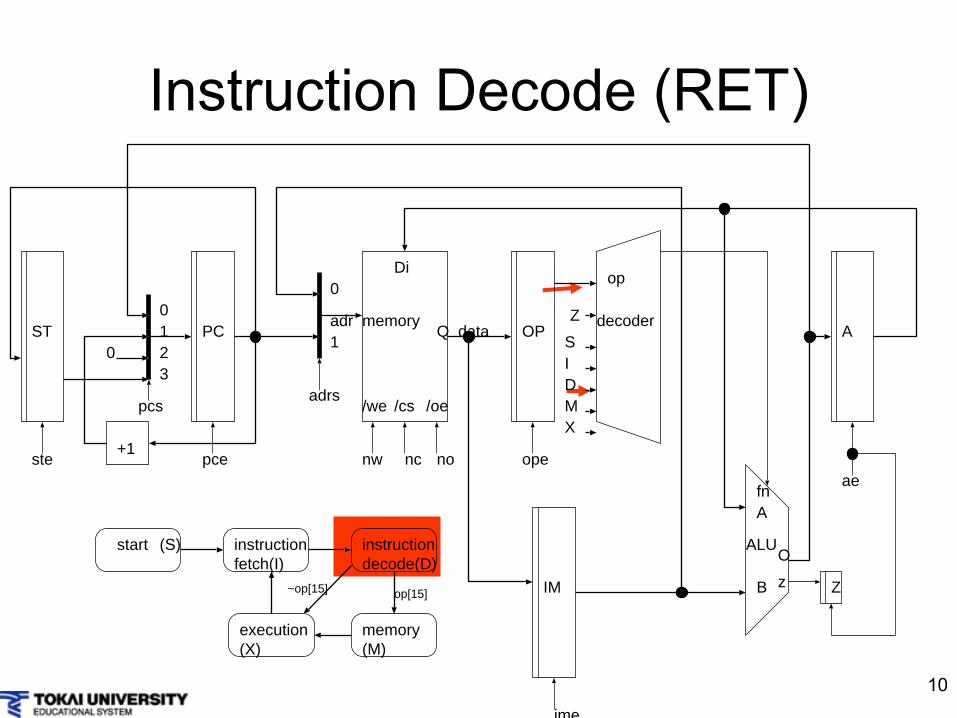
Instruction Decode (RET)
PC OPmemoryadr
data
/cs /oe
+1
IM
Q
Di
/we
0A
opeae
ime
pce
pcs
nw nonc
adrs
ALU
fnA
B
00
11
2
decoder
start instructionfetch(I)
instructiondecode(D)
execution(X)
(S)
SIDM
op
O
z Z
Z
memory(M)
op[15]~op[15]
X
ST
ste
3
11
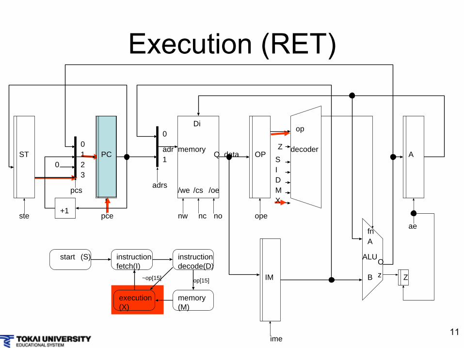
Execution (RET)
PC OPmemoryadr
data
/cs /oe
+1
IM
Q
Di
/we
0A
opeae
ime
pce
pcs
nw nonc
adrs
ALU
fnA
B
00
11
2
decoder
start instructionfetch(I)
instructiondecode(D)
execution(X)
(S)
SIDM
op
O
z Z
Z
memory(M)
op[15]~op[15]
X
ST
ste
3

12
Truth table of the decoder
S I D X
pcs
pce
adrs
ope
ime
ae nw nc no fn
1 0 0 0
0 1 0 0
0 0 1 0
0 0 0 1
M
0
0
0
0
0 0 0 01
ste
13
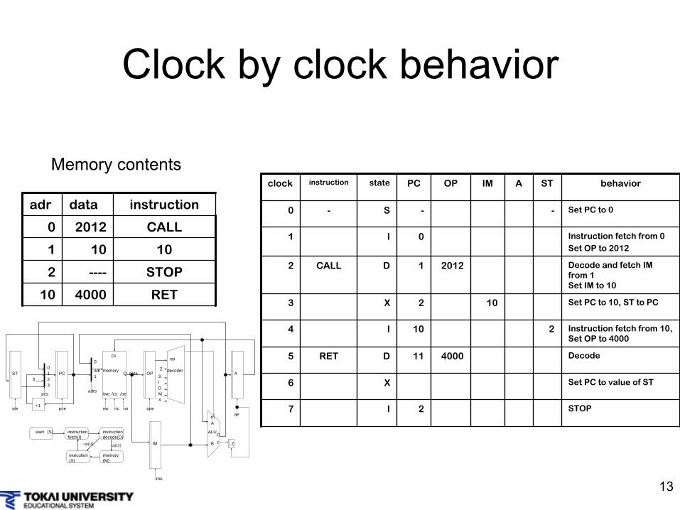
Clock by clock behavior
adr data instruction
0 2012 CALL
1 10 10
2 ---- STOP
10 4000 RET
Memory contents
PC OPmemoryadr
data
/cs /oe
+1
IM
Q
Di
/we
0A
opeae
ime
pce
pcs
nw nonc
adrs
ALU
fnA
B
00
11
2
decoder
start instructionfetch(I)
instructiondecode(D)
execution(X)
(S)
SIDM
op
O
z Z
Z
memory(M)
op[15]~op[15]
X
ST
ste
3
clock instruction state PC OP IM A ST behavior
0 - S - - Set PC to 0
1 I 0 Instruction fetch from 0Set OP to 2012
2 CALL D 1 2012 Decode and fetch IM from 1
Set IM to 10
3 X 2 10 Set PC to 10, ST to PC
4 I 10 2 Instruction fetch from 10, Set OP to 4000
5 RET D 11 4000 Decode
6 X Set PC to value of ST
7 I 2 STOP
14
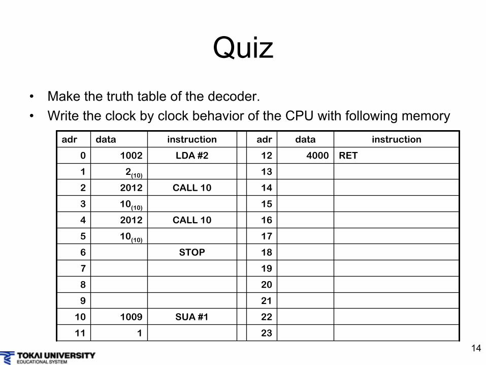
Quiz•
Make the truth table of the decoder.•
Write the clock by clock behavior of the CPU with following memoryadr data instruction adr data instruction
0 1002 LDA #2 12 4000 RET
1 2(10) 13
2 2012 CALL 10 14
3 10(10) 15
4 2012 CALL 10 16
5 10(10) 17
6 STOP 18
7 19
8 20
9 21
10 1009 SUA #1 22
11 1 23