Universität Dortmund
Laboratory Exercise 6
Davide Rossi
DEI University of Bologna
AA 2016-2017

Universität Dortmund
Simple System Busses
• The primary goal of a simple system bus is to allow software (running on a processor) to communicate with other hardware in the SoC
• There are many different implementation ... but they are all very similar

Universität Dortmund
Embedded Processor I/O
• RISC-based embedded processors communicate with external hardware using two simple instructions:
– Load Operation: Copies a word of data from a specific address to a local register
– Store Operation: Copies a word of data from a local register to a specific address

Universität Dortmund
Embedded Processor I/O
Software
sets up the
register with
the address
and data ...
Blocks
decode
addresses
to see if
they are the
targets...
Data
transferred
between
register and
hardware
EXT MEM
MEMORY

Universität Dortmund
APB BUS

Universität Dortmund
APB BUS SIGNALS

Universität Dortmund
APB BUS: SLAVE INTERFACE
APB PERIPHERAL
PCLK
PRESETn
PADDR
PSEL
PENABLE
PWRITE
PWDATA
PRDATA
PREADY
PSLVERR
Universität Dortmund
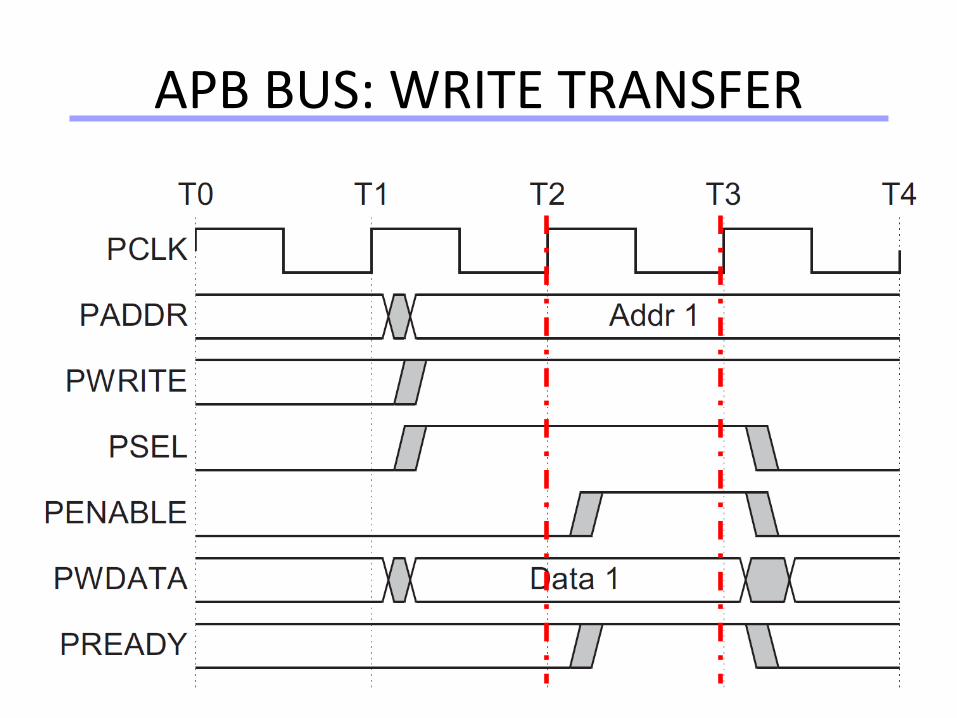
APB BUS: WRITE TRANSFER

Universität Dortmund
APB BUS: READ TRANSFER
Universität Dortmund
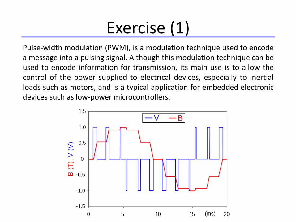
Exercise (1)Pulse-width modulation (PWM), is a modulation technique used to encodea message into a pulsing signal. Although this modulation technique can beused to encode information for transmission, its main use is to allow thecontrol of the power supplied to electrical devices, especially to inertialloads such as motors, and is a typical application for embedded electronicdevices such as low-power microcontrollers.
Universität Dortmund
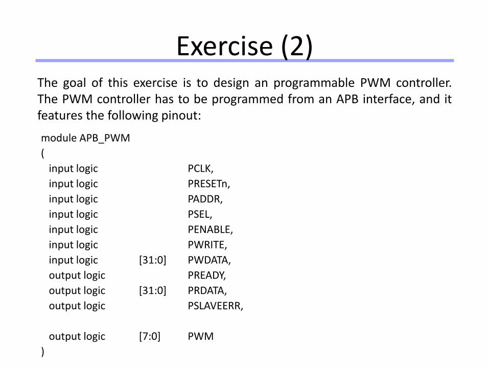
Exercise (2)The goal of this exercise is to design an programmable PWM controller.The PWM controller has to be programmed from an APB interface, and itfeatures the following pinout:
module APB_PWM
(
input logic PCLK,
input logic PRESETn,
input logic PADDR,
input logic PSEL,
input logic PENABLE,
input logic PWRITE,
input logic [31:0] PWDATA,
output logic PREADY,
output logic [31:0] PRDATA,
output logic PSLAVEERR,
output logic [7:0] PWM
)
Universität Dortmund
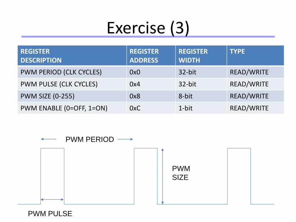
Exercise (3)REGISTERDESCRIPTION
REGISTERADDRESS
REGISTER WIDTH
TYPE
PWM PERIOD (CLK CYCLES) 0x0 32-bit READ/WRITE
PWM PULSE (CLK CYCLES) 0x4 32-bit READ/WRITE
PWM SIZE (0-255) 0x8 8-bit READ/WRITE
PWM ENABLE (0=OFF, 1=ON) 0xC 1-bit READ/WRITE
PWM PERIOD
PWM PULSE
PWM
SIZE

Universität Dortmund
Exercise (4)
1) Design a block diagram of the digital circuit2) Design the memory mapped APB registers using
system verilog hardware description3) Design the PWM FSM using system verilog
hardware description language4) Design a testbench to validate the functionality
of the designed digital circuit
Design the digital circuit in a modular way (i.e. Design every digital block in a separate system
verilog module)
Recommended