Tutorial ITutorial I
Circuit SimulationCircuit Simulation
Boonchuay SupmonchaiIntegrated Design Application Research (IDAR) Laboratory
June 24, 2005

2102-545 Digital ICs2102-545 Digital ICs SPICE Simulations 2
B.SupmonchaiB.Supmonchai
OutlineOutline Introduction to SPICE
Basic Commands and elements in SPICE
SPICE MOSFET models
Device Characterization
Pitfalls and Fallacies
2102-545 Digital ICs2102-545 Digital ICs SPICE Simulations 3
B.SupmonchaiB.Supmonchai
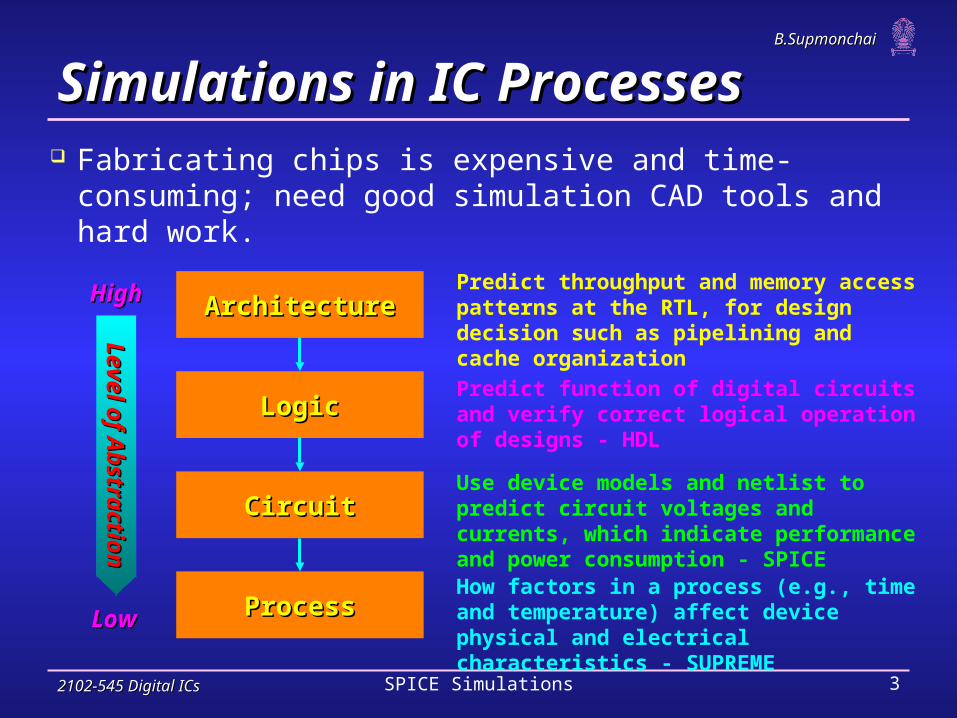
Simulations in IC ProcessesSimulations in IC Processes Fabricating chips is expensive and time-consuming;
need good simulation CAD tools and hard work.
ArchitectureArchitecture
CircuitCircuit
ProcessProcess
LogicLogic
Level o
f Ab
straction
Level o
f Ab
straction
HighHigh
LowLowHow factors in a process (e.g., time and temperature) affect device physical and electrical characteristics - SUPREME
Use device models and netlist to predict circuit voltages and currents, which indicate performance and power consumption - SPICE
Predict function of digital circuits and verify correct logical operation of designs - HDL
Predict throughput and memory access patterns at the RTL, for design decision such as pipelining and cache organization

2102-545 Digital ICs2102-545 Digital ICs SPICE Simulations 4
B.SupmonchaiB.Supmonchai
Introduction to SPICEIntroduction to SPICE SSimulation PProgram with IIntegrated CCircuit EEmphasis
Developed in 1970’s at Berkeley
Written in FORTRAN for punch-card machines Circuits elements are called cards
Complete description is called a SPICE deckSPICE deck
SPICE has been regarded as de facto standard in circuit simulation.
Commercial releases of SPICE (e.g., PSPICE and HSPICE) typically contain a much larger selection of refined models.

2102-545 Digital ICs2102-545 Digital ICs SPICE Simulations 5
B.SupmonchaiB.Supmonchai
SPICE DecksSPICE Decks Writing a SPICE deck is like writing a good
program PlanPlan: sketch schematic on paper or in editor
Modify existing decks whenever possible
CodeCode: strive for clarity Start with name, email, date, purpose Generously comment
TestTest: Predict what results should be Compare with actual Garbage In, Garbage Out!Garbage In, Garbage Out!

2102-545 Digital ICs2102-545 Digital ICs SPICE Simulations 6
B.SupmonchaiB.Supmonchai
SPICE ElementsSPICE ElementsLetterLetter ElementElementR ResistorC CapacitorL InductorK Mutual InductorV Independent voltage sourceI Independent current sourceM MOSFETD DiodeQ Bipolar transistorW Lossy transmission lineX SubcircuitE Voltage-controlled voltage sourceG Voltage-controlled current sourceH Current-controlled voltage sourceF Current-controlled current source

2102-545 Digital ICs2102-545 Digital ICs SPICE Simulations 7
B.SupmonchaiB.Supmonchai
Units in SPICEUnits in SPICE
LetterLetter UnitUnit MagnitudeMagnitude
aa attoatto 1010-18-18
ff femtofemto 1010-15-15
pp picopico 1010-12-12
nn nanonano 1010-9-9
uu micromicro 1010-6-6
mm millimilli 1010-3-3
kk kilokilo 101033
xx megamega 101066
gg gigagiga 101099
Ex: 100 femtofarad capacitor = 100fF, 100f, 100e-15Ex: 100 femtofarad capacitor = 100fF, 100f, 100e-15

2102-545 Digital ICs2102-545 Digital ICs SPICE Simulations 8
B.SupmonchaiB.Supmonchai
SourcesSources DC Source
Vdd vdd gnd 2.5Vdd vdd gnd 2.5
Piecewise Linear SourceVin in gnd pwl 0ps 0 100ps 0 150ps 1.8 800ps 1.8Vin in gnd pwl 0ps 0 100ps 0 150ps 1.8 800ps 1.8
Pulsed SourceVck clk gnd PULSE 0 1.8 0ps 100ps 100ps 300ps 800psVck clk gnd PULSE 0 1.8 0ps 100ps 100ps 300ps 800ps
PULSE v1 v2 td tr tf pw per
v1
v2
td tr tfpw
per

2102-545 Digital ICs2102-545 Digital ICs SPICE Simulations 9
B.SupmonchaiB.Supmonchai
Example: RC CircuitExample: RC Circuit
* rc.sp* rc.sp* [email protected] 2/2/03* [email protected] 2/2/03* Find the response of RC circuit to rising input* Find the response of RC circuit to rising input
*------------------------------------------------*------------------------------------------------* Parameters and models* Parameters and models*------------------------------------------------*------------------------------------------------.option post.option post
*------------------------------------------------*------------------------------------------------* Simulation netlist* Simulation netlist*------------------------------------------------*------------------------------------------------VinVin inin gndgnd pwlpwl 0ps 0 100ps 0 150ps 1.8 800ps 1.80ps 0 100ps 0 150ps 1.8 800ps 1.8R1R1 inin outout 2k2kC1C1 outout gndgnd 100f100f
*------------------------------------------------*------------------------------------------------* Stimulus* Stimulus*------------------------------------------------*------------------------------------------------.tran 20ps 800ps.tran 20ps 800ps.plot v(in) v(out).plot v(in) v(out).end.end
R1 = 2KΩR1 = 2KΩ
C1 = 100fFC1 = 100fFVinVin
+VoutVout
-

2102-545 Digital ICs2102-545 Digital ICs SPICE Simulations 10
B.SupmonchaiB.Supmonchai
RC Circuit Result (Textual)RC Circuit Result (Textual)legend:
legend:
a: v(in)
a: v(in)
b: v(out)
b: v(out)
time v(in)
time v(in)
(ab ) 0. 500.0000m 1.0000 1.5000 2.0000
(ab ) 0. 500.0000m 1.0000 1.5000 2.0000
+ + + + +
+ + + + +
0. 0. -2------+------+------+------+------+------+------+------
0. 0. -2------+------+------+------+------+------+------+------
+-+-
20.0000p 0. 2 + + + + + + + +
20.0000p 0. 2 + + + + + + + +
40.0000p 0. 2 + + + + + + + +
40.0000p 0. 2 + + + + + + + +
60.0000p 0. 2 + + + + + + + +
60.0000p 0. 2 + + + + + + + +
80.0000p 0. 2 + + + + + + + +
80.0000p 0. 2 + + + + + + + +
100.0000p 0. 2 + + + + + + + +
100.0000p 0. 2 + + + + + + + +
120.0000p 720.000m +
120.0000p 720.000m + bb + +
+ + aa + + + + + +
+ + + + + +
140.0000p 1.440 +
140.0000p 1.440 + bb + + + + +
+ + + + + aa + + +
+ + +
160.0000p 1.800 + +
160.0000p 1.800 + + bb + + + + + +
+ + + + + + aa +
+
180.0000p 1.800 + +
180.0000p 1.800 + + bb + + + + + +
+ + + + + + aa +
+
200.0000p 1.800 -+------+------+
200.0000p 1.800 -+------+------+ bb -----+------+------+------+------+
-----+------+------+------+------+ aa -----
-----
+-+-
220.0000p 1.800 + + +
220.0000p 1.800 + + + bb + + + + +
+ + + + + aa +
+
240.0000p 1.800 + + + +
240.0000p 1.800 + + + + bb + + + +
+ + + + aa +
+
260.0000p 1.800 + + + +
260.0000p 1.800 + + + + bb + + + +
+ + + + aa +
+
280.0000p 1.800 + + + +
280.0000p 1.800 + + + + bb + + + +
+ + + + aa +
+
300.0000p 1.800 + + + + +
300.0000p 1.800 + + + + + bb + + +
+ + + aa +
+
320.0000p 1.800 + + + + +
320.0000p 1.800 + + + + + bb + + +
+ + + aa +
+
340.0000p 1.800 + + + + +
340.0000p 1.800 + + + + + bb + + +
+ + + aa +
+
360.0000p 1.800 + + + + +
360.0000p 1.800 + + + + + bb + +
+ + aa +
+
380.0000p 1.800 + + + + + +
380.0000p 1.800 + + + + + + bb + +
+ + aa +
+
400.0000p 1.800 -+------+------+------+------+------+--
400.0000p 1.800 -+------+------+------+------+------+-- bb ---+------+
---+------+ aa -----
-----
+-+-
420.0000p 1.800 + + + + + +
420.0000p 1.800 + + + + + + bb + +
+ + aa +
+
440.0000p 1.800 + + + + + +
440.0000p 1.800 + + + + + + bb + +
+ + aa +
+
460.0000p 1.800 + + + + + +
460.0000p 1.800 + + + + + + bb + +
+ + aa +
+
480.0000p 1.800 + + + + + +
480.0000p 1.800 + + + + + + bb +
+ aa +
+
500.0000p 1.800 + + + + + + +
500.0000p 1.800 + + + + + + + bb +
+ aa +
+
520.0000p 1.800 + + + + + + +
520.0000p 1.800 + + + + + + + bb +
+ aa +
+
540.0000p 1.800 + + + + + + +
540.0000p 1.800 + + + + + + + bb +
+ aa +
+
560.0000p 1.800 + + + + + + +
560.0000p 1.800 + + + + + + + bb +
+ aa +
+
580.0000p 1.800 + + + + + + +
580.0000p 1.800 + + + + + + + bb +
+ aa +
+
600.0000p 1.800 -+------+------+------+------+------+------+---
600.0000p 1.800 -+------+------+------+------+------+------+--- bb --+
--+ aa -----
-----
+-+-
620.0000p 1.800 + + + + + + +
620.0000p 1.800 + + + + + + + bb +
+ aa +
+
640.0000p 1.800 + + + + + + +
640.0000p 1.800 + + + + + + + bb + + aa +
+
660.0000p 1.800 + + + + + + +
660.0000p 1.800 + + + + + + + bb + + aa +
+
680.0000p 1.800 + + + + + + +
680.0000p 1.800 + + + + + + + bb + + aa +
+
700.0000p 1.800 + + + + + + +
700.0000p 1.800 + + + + + + + bb ++ aa +
+
720.0000p 1.800 + + + + + + +
720.0000p 1.800 + + + + + + + bb ++ aa +
+
740.0000p 1.800 + + + + + + +
740.0000p 1.800 + + + + + + + bb ++ aa +
+
760.0000p 1.800 + + + + + + +
760.0000p 1.800 + + + + + + + bb ++ aa +
+
780.0000p 1.800 + + + + + + +
780.0000p 1.800 + + + + + + + bb aa +
+
800.0000p 1.800 -+------+------+------+------+------+------+------
800.0000p 1.800 -+------+------+------+------+------+------+------ bb aa -----
-----
+-+-
+ + + + +
+ + + + +
2102-545 Digital ICs2102-545 Digital ICs SPICE Simulations 11
B.SupmonchaiB.Supmonchai
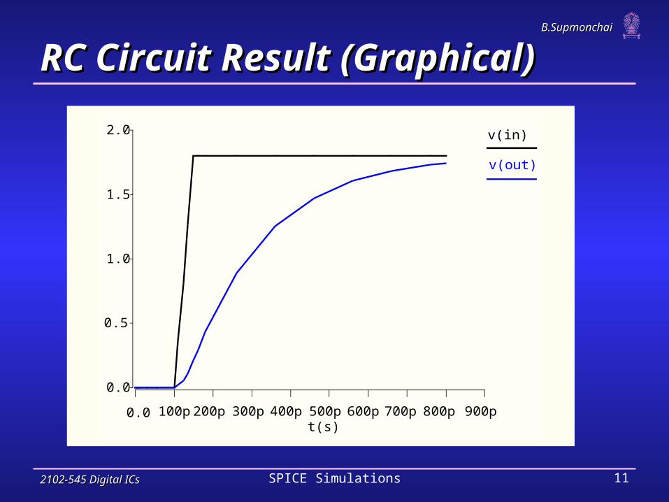
RC Circuit Result (Graphical)RC Circuit Result (Graphical)
t(s)0.0 100p 200p 300p 400p 500p 600p 700p 800p 900p
0.0
0.5
1.0
1.5
2.0 v(in)
v(out)

2102-545 Digital ICs2102-545 Digital ICs SPICE Simulations 12
B.SupmonchaiB.Supmonchai
MOSFET ElementsMOSFET Elements M element for MOSFET
M1 3 1 0 0 NMOD L=1U W=10U AD=120P PD=42UM1 3 1 0 0 NMOD L=1U W=10U AD=120P PD=42U
Mname drain gate source body typeMname drain gate source body type
+ W=<width> L=<length>+ W=<width> L=<length>
+ AS=<area source> AD = <area drain> + AS=<area source> AD = <area drain>
+ PS=<perimeter source> PD=<perimeter drain>+ PS=<perimeter source> PD=<perimeter drain>
Example:
Node NameNode Name

2102-545 Digital ICs2102-545 Digital ICs SPICE Simulations 13
B.SupmonchaiB.Supmonchai
MOSFET ModelsMOSFET Models Earlier SPICE versions had three built-in
MOSFET models: LEVEL 1 (MOS1)LEVEL 1 (MOS1) - Square law I-V characteristic
LEVEL 2 (MOS2)LEVEL 2 (MOS2) - Detailed analytical MOSFET
LEVEL 3 (MOS3)LEVEL 3 (MOS3) - Semi-empirical
MOS2 and MOS3 include second-order effects such as velocity saturation, mobility degradation, subthreshold conduction, and DIBL.
All three LEVELs do not provide good fits to the characteristics of modern devices.

2102-545 Digital ICs2102-545 Digital ICs SPICE Simulations 14
B.SupmonchaiB.Supmonchai
MOSFET Models (2)MOSFET Models (2) For modern submicron devices, the Berkeley
Short-Channel IGFET Model (BSIM) is the most widely used (commercially and academically). BSIM version 1, 2, 3v3, and 4 are implemented as
SPICE level 13, 39, 49, and 54, respectively
BSIM is a very elaborate model that are derived from the underlying device physics but use an enormous number of parameters to fit the behavior of modern transistor. BSIM version 3v3 requires over 27 pages of over 100
parameters and device equations to describe the model.

2102-545 Digital ICs2102-545 Digital ICs SPICE Simulations 15
B.SupmonchaiB.Supmonchai
Selection of ModelsSelection of Models The level (type) of MOSFET model to be used
in a particular simulation can be specified through the .MODEL statement in SPICE.
With the statement, the user can describe a large number of model parameters including geometry of the device such as channel length and width.
M1 3 1 0 0 NMOD L=1U W=10U AD=120P PD=42UM1 3 1 0 0 NMOD L=1U W=10U AD=120P PD=42U
MDEV32 14 9 12 5 PMOD L=1.2U W=20UMDEV32 14 9 12 5 PMOD L=1.2U W=20U
.MODEL NMOD NMOS (.MODEL NMOD NMOS (LEVEL=1LEVEL=1 VTO=1.4 KP=4.5E-5 CBD=5PF CBS=2PF) VTO=1.4 KP=4.5E-5 CBD=5PF CBS=2PF)
.MODEL PMOD PMOS (VTO=-2 KP=3.0E-5 LAMBDA=0.02 GAMMA=0.4.MODEL PMOD PMOS (VTO=-2 KP=3.0E-5 LAMBDA=0.02 GAMMA=0.4+ CBD=4PF CBS=2PF RD=5 RS=3 CGDO=1PF+ CBD=4PF CBS=2PF RD=5 RS=3 CGDO=1PF++ CGSO=1PF CGBO=1PF) CGSO=1PF CGBO=1PF)

2102-545 Digital ICs2102-545 Digital ICs SPICE Simulations 16
B.SupmonchaiB.Supmonchai
NMOS Transistor Circuit ModelNMOS Transistor Circuit Model

2102-545 Digital ICs2102-545 Digital ICs SPICE Simulations 17
B.SupmonchaiB.Supmonchai
LEVEL 1 Model EquationsLEVEL 1 Model Equations Corresponding to our unified model for manual
analyses in the class.
Basic Current Models:
€
IDS =
⎧
⎨ ⎪ ⎪
⎩ ⎪ ⎪
0 VGS < VT cutoff
k 'Weff
Leff
1+ λ ⋅VDS( ) VGS −VT −VDS
2
⎛
⎝ ⎜
⎞
⎠ ⎟⋅VDS VDS < VGS −VT linear
k'
2
Weff
Leff
1+ λ ⋅VDS( ) VGS −VT( )2
VDS > VGS −VT saturation
€
Vt = VT 0 +γ 2φF −VSB − 2φF( )where

2102-545 Digital ICs2102-545 Digital ICs SPICE Simulations 18
B.SupmonchaiB.Supmonchai
LEVEL 1 Model Equations (II)LEVEL 1 Model Equations (II) Completely characterized by the five electrical
parameters: k’, VT0, , |2F|, and (KPKP, , VTOVTO, ,
GAMMAGAMMA, , PHIPHI, and , and LAMBDALAMBDA in SPICE)
Physical parameters, e.g., tox (TOXTOX) can be specified in stead of the electrical parameters.
If both present simultaneously in the model, electrical parameters always overrideoverride physical parameters.
Though grossly inaccurate, LEVEL 1 offers a quick, useful estimate of the circuits.

2102-545 Digital ICs2102-545 Digital ICs SPICE Simulations 19
B.SupmonchaiB.Supmonchai
LEVEL 2 and 3 Model EquationsLEVEL 2 and 3 Model Equations Improved models for the drain current
Level 2: A number of semi-empirical corrections have been added to the basic equations.
Level 3: Majority of the model equations are empirical Improving accuracy Reducing complexity in calculation.
Although more accurate, LEVEL 2 and 3 models are still insufficient to achieve good agreement with experimental data for the deep submicron devices.
2102-545 Digital ICs2102-545 Digital ICs SPICE Simulations 20
B.SupmonchaiB.Supmonchai
Parasitic CapacitancesParasitic Capacitances SPICE models use separate sets of equations in
cut-off, linear, and saturation modes to calculate the device parasitic capacitances.
Gate Capacitances: SPICE uses a simple model that represents the charge storage effect by three nonlinear two-terminal capacitors: CCGBGB, CCGSGS, and
CCGDGD (please see chapter 2 for the detail)
Required geometry information: gate oxide thickness (TOXTOX), channel width (WW), channel length (LL), and the lateral diffusion (LDLD).

2102-545 Digital ICs2102-545 Digital ICs SPICE Simulations 21
B.SupmonchaiB.Supmonchai
Parasitic Capacitances (2)Parasitic Capacitances (2) Junction Capacitance: SPICE uses the simple
pn-junction model to simulate the parasitic capacitances of the source and drain diffusion regions.
€
CSB =C j ⋅ AS
1+VSB
φ0
⎛
⎝ ⎜
⎞
⎠ ⎟
M j+
C jsw ⋅PS
1+VSB
φ0
⎛
⎝ ⎜
⎞
⎠ ⎟
M jsw
CDB =C j ⋅ AD
1+VDB
φ0
⎛
⎝ ⎜
⎞
⎠ ⎟
M j+
C jsw ⋅PD
1+VDB
φ0
⎛
⎝ ⎜
⎞
⎠ ⎟
M jsw
where AS and AD are the source and the drain areas; PS and PD are the source and the drain perimeters, respectively

2102-545 Digital ICs2102-545 Digital ICs SPICE Simulations 22
B.SupmonchaiB.Supmonchai
Parasitic Capacitances (3)Parasitic Capacitances (3) Cj is the zero-bias depletion capacitance per unit area at
the bottom plate of the drain or the source diffusion region. (CJCJ in SPICE)
Cjsw is the zero-bias depletion capacitance per unit length at the side-wall plate. (CJSWCJSW)
Mj and Mjsw are the junction degrading coefficients of the bottom and side-wall plates, respectively. (MJMJ, MJSWMJSW) 0.5 for abrupt juction and 0.33 for linearly graded junction
00 is the built-in junction potential which is actually a function of the doping densities (PBPB for bottom plate and PHPPHP (MOS) or PBSWPBSW (BSIM) for side walls)

2102-545 Digital ICs2102-545 Digital ICs SPICE Simulations 23
B.SupmonchaiB.Supmonchai
Example: NMOS I-V CharacteristicsExample: NMOS I-V Characteristics
* mosiv.sp* mosiv.sp
*------------------------------------------------*------------------------------------------------* Parameters and models* Parameters and models*------------------------------------------------*------------------------------------------------.include '../models/tsmc180/models.sp'.include '../models/tsmc180/models.sp'.temp 70.temp 70.option post.option post
*------------------------------------------------*------------------------------------------------ * Simulation netlist* Simulation netlist*------------------------------------------------*------------------------------------------------*nmos*nmosVgsVgs gg gndgnd 00VdsVds dd gndgnd 00M1M1 dd gg gndgnd gndgnd NMOSNMOS W=0.36uW=0.36u L=0.18uL=0.18u
*------------------------------------------------*------------------------------------------------* Stimulus* Stimulus*------------------------------------------------*------------------------------------------------.dc Vds 0 1.8 0.05 SWEEP Vgs 0 1.8 0.3.dc Vds 0 1.8 0.05 SWEEP Vgs 0 1.8 0.3.end.end
VVgsgs VVdsds
IIdsds
4/24/2
2102-545 Digital ICs2102-545 Digital ICs SPICE Simulations 24
B.SupmonchaiB.Supmonchai
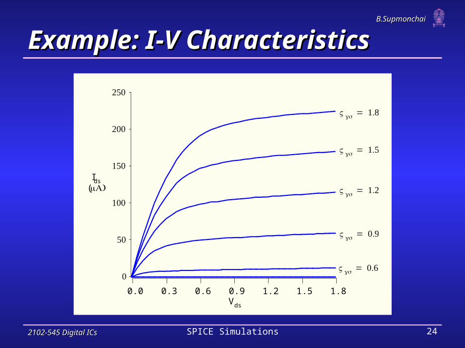
Example: I-V CharacteristicsExample: I-V Characteristics
Vds
0.0 0.3 0.6 0.9 1.2 1.5 1.8
Ids(μ )A
0
50
100
150
200
250
Vgs = 1.8
Vgs = 1.5
Vgs = 1.2
Vgs = 0.9
Vgs = 0.6

2102-545 Digital ICs2102-545 Digital ICs SPICE Simulations 25
B.SupmonchaiB.Supmonchai
Example: Inverter Transient AnalysisExample: Inverter Transient Analysis•inv.spinv.sp
* Parameters and models* Parameters and models*------------------------------------------------*------------------------------------------------.param SUPPLY=1.8.param SUPPLY=1.8.option scale=90n.option scale=90n.include '../models/tsmc180/models.sp'.include '../models/tsmc180/models.sp'.temp 70.temp 70.option post.option post
* Simulation netlist* Simulation netlist*------------------------------------------------*------------------------------------------------VddVdd vddvdd gndgnd 'SUPPLY''SUPPLY'VinVin aa gndgnd PULSEPULSE 0 'SUPPLY' 50ps 0ps 0ps 100ps 200ps0 'SUPPLY' 50ps 0ps 0ps 100ps 200psM1M1 yy aa gndgnd gndgnd NMOSNMOS W=4W=4 L=2 L=2 + AS=20 PS=18 AD=20 PD=18+ AS=20 PS=18 AD=20 PD=18M2M2 yy aa vddvdd vddvdd PMOSPMOS W=8W=8 L=2L=2+ AS=40 PS=26 AD=40 PD=26+ AS=40 PS=26 AD=40 PD=26
* Stimulus* Stimulus*------------------------------------------------*------------------------------------------------.tran 1ps 200ps.tran 1ps 200ps.end.end
aayy
4/2
8/2
**Unloaded inverter****Unloaded inverter**

2102-545 Digital ICs2102-545 Digital ICs SPICE Simulations 26
B.SupmonchaiB.Supmonchai
Example: Inverter Transient ResultsExample: Inverter Transient Results
(V)
0.0
1.0
t(s)0.0 50p 100p 150p 200p
v(a)
v(y)
tpdr = 15pstpdf = 12ps
tf = 10ps
tr = 16ps
0.36
1.44
1.8
OvershootOvershoot
Very fast Very fast edgesedges
2102-545 Digital ICs2102-545 Digital ICs SPICE Simulations 27
B.SupmonchaiB.Supmonchai
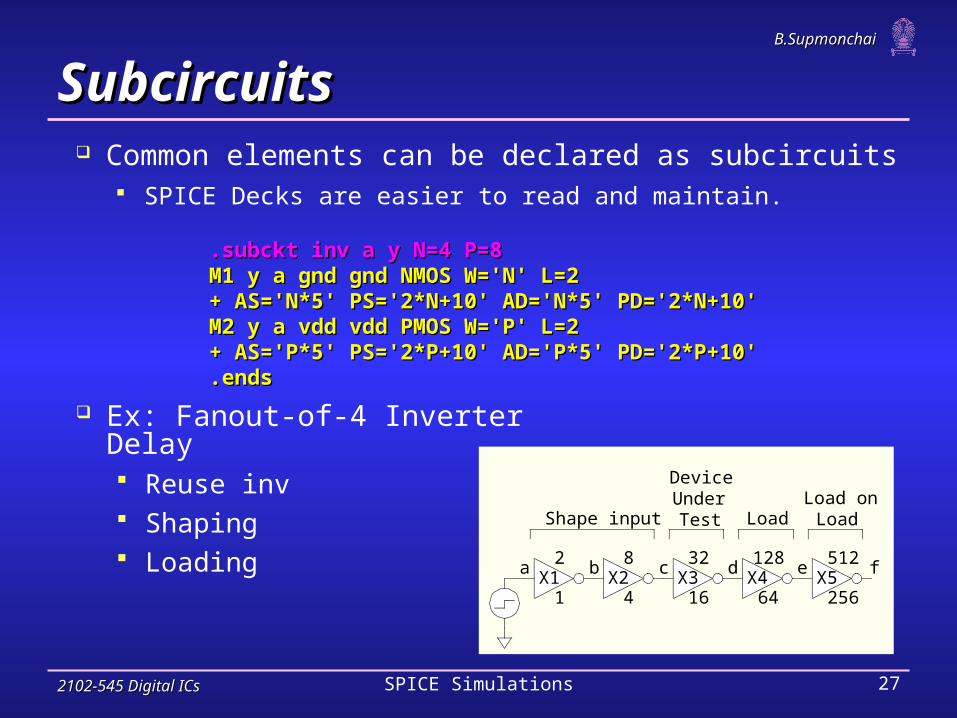
SubcircuitsSubcircuits Common elements can be declared as subcircuits
SPICE Decks are easier to read and maintain.
.subckt inv a y N=4 P=8.subckt inv a y N=4 P=8M1 y a gnd gnd NMOS W='N' L=2 M1 y a gnd gnd NMOS W='N' L=2 + AS='N*5' PS='2*N+10' AD='N*5' PD='2*N+10'+ AS='N*5' PS='2*N+10' AD='N*5' PD='2*N+10'M2 y a vdd vdd PMOS W='P' L=2M2 y a vdd vdd PMOS W='P' L=2+ AS='P*5' PS='2*P+10' AD='P*5' PD='2*P+10'+ AS='P*5' PS='2*P+10' AD='P*5' PD='2*P+10'.ends.ends
a b c d eX1 X2 X3 X4
1
2
4
8
16
32
64
128 fX5
256
512
Shape input
DeviceUnderTest Load
Load onLoad
Ex: Fanout-of-4 Inverter Delay Reuse inv Shaping Loading

2102-545 Digital ICs2102-545 Digital ICs SPICE Simulations 28
B.SupmonchaiB.Supmonchai
Example: FO4 Inverter DelayExample: FO4 Inverter Delay
* fo4.sp* fo4.sp
* Parameters and models* Parameters and models*----------------------------------------------------------------------*----------------------------------------------------------------------.param SUPPLY=1.8.param SUPPLY=1.8.param H=4.param H=4.option scale=90n.option scale=90n.include '../models/tsmc180/models.sp'.include '../models/tsmc180/models.sp'.temp 70.temp 70.option post.option post
* Subcircuits* Subcircuits*----------------------------------------------------------------------*----------------------------------------------------------------------.global vdd gnd.global vdd gnd.include '../lib/inv.sp'.include '../lib/inv.sp'
* Simulation netlist* Simulation netlist*----------------------------------------------------------------------*----------------------------------------------------------------------VddVdd vddvdd gndgnd 'SUPPLY''SUPPLY'VinVin aa gndgnd PULSEPULSE 0 'SUPPLY' 0ps 100ps 100ps 500ps 1000ps0 'SUPPLY' 0ps 100ps 100ps 500ps 1000psX1X1 aa bb invinv * shape input waveform * shape input waveformX2X2 bb cc invinv M='H' * reshape input waveformM='H' * reshape input waveform

2102-545 Digital ICs2102-545 Digital ICs SPICE Simulations 29
B.SupmonchaiB.Supmonchai
Example: FO4 Inverter Delay (2)Example: FO4 Inverter Delay (2)
X3X3 cc dd invinv M='H**2' * device under testM='H**2' * device under testX4X4 dd ee invinv M='H**3' * loadM='H**3' * loadx5x5 ee ff invinv M='H**4' * load on loadM='H**4' * load on load
* Stimulus* Stimulus*----------------------------------------------------------------------*----------------------------------------------------------------------.tran 1ps 1000ps.tran 1ps 1000ps.measure tpdr.measure tpdr * rising prop delay* rising prop delay+ TRIG v(c)+ TRIG v(c) VAL='SUPPLY/2' FALL=1 VAL='SUPPLY/2' FALL=1 + TARG v(d) + TARG v(d) VAL='SUPPLY/2' RISE=1VAL='SUPPLY/2' RISE=1.measure tpdf.measure tpdf * falling prop delay* falling prop delay+ TRIG v(c) + TRIG v(c) VAL='SUPPLY/2' RISE=1VAL='SUPPLY/2' RISE=1+ TARG v(d) + TARG v(d) VAL='SUPPLY/2' FALL=1 VAL='SUPPLY/2' FALL=1 .measure tpd param='(tpdr+tpdf)/2'.measure tpd param='(tpdr+tpdf)/2' * average prop delay* average prop delay.measure trise.measure trise * rise time* rise time++ TRIG v(d)TRIG v(d) VAL='0.2*SUPPLY' RISE=1VAL='0.2*SUPPLY' RISE=1++ TARG v(d)TARG v(d) VAL='0.8*SUPPLY' RISE=1VAL='0.8*SUPPLY' RISE=1.measure tfall.measure tfall * fall time* fall time++ TRIG v(d)TRIG v(d) VAL='0.8*SUPPLY' FALL=1VAL='0.8*SUPPLY' FALL=1++ TARG v(d)TARG v(d) VAL='0.2*SUPPLY' FALL=1VAL='0.2*SUPPLY' FALL=1.end .end

2102-545 Digital ICs2102-545 Digital ICs SPICE Simulations 30
B.SupmonchaiB.Supmonchai
Example: FO4 Inverter Delay ResultsExample: FO4 Inverter Delay Results
(V)
0.0
0.5
1.0
1.5
2.0
t(s)0.0 200p 400p 600p 800p 1n
a
b
c
d
e
ftpdf = 66ps tpdr = 83ps

2102-545 Digital ICs2102-545 Digital ICs SPICE Simulations 31
B.SupmonchaiB.Supmonchai
Device CharacterizationDevice Characterization Modern SPICE models are so complicated that
the designer cannot easily read key performance characteristics from the model files.
A more convenient approach is to run a set of simulations and then extract parameters and other interesting data, e.g., I-V characteristics, threshold voltage, effective resistance and capacitance. Various methods to find these parameters and the
required simulations are described in the literature.

2102-545 Digital ICs2102-545 Digital ICs SPICE Simulations 32
B.SupmonchaiB.Supmonchai
Device Characteristics ComparisonDevice Characteristics Comparison

2102-545 Digital ICs2102-545 Digital ICs SPICE Simulations 33
B.SupmonchaiB.Supmonchai
Pitfalls and FallaciesPitfalls and Fallacies Failing to estimate diffusion and interconnect parasitics
in simulations Diffusion capacitance can account for more than 50% of the
delay of a high fan-in, low fanout gate. Make sure that the area and perimeter of the source and drain are included in the simulation.
RC delay of the long wires dominate the path delay but it is difficult to estimate.
Good models describe not only the circuit but also the input edge rates, the output loading, and parasitics such as diffusion capacitance and interconnect. Gate delay is strongly dependent on the rise/fall time of the
input and even more strongly on the output loading

2102-545 Digital ICs2102-545 Digital ICs SPICE Simulations 34
B.SupmonchaiB.Supmonchai
Pitfalls and Fallicies (2)Pitfalls and Fallicies (2) SPICE is prone to Garbage in, Garbage out! So
do not blindly trust the results from SPICE. Failing to account for hidden scale factors
Identifying incorrect critical path
Choosing inappropriate transistor sizes Compare results of a design with carefully selected
transistor sizes to a convention design with poorly selected sizes.
Do not use SPICE in place of thinking Do not use SPICE too much. Circuit simulation
should be guided by analysis

2102-545 Digital ICs2102-545 Digital ICs SPICE Simulations 35
B.SupmonchaiB.Supmonchai
Pitfalls and Fallacies (3)Pitfalls and Fallacies (3) Rule of Thumbs:
““Assume SPICE decks are buggy until proven otherwise.”Assume SPICE decks are buggy until proven otherwise.”
If the simulation does not agree with your expectations, look closely for errors or inadequate modeling in the deck.
Motto: Check and Recheck!
Recommended