1
Tutorial 9 (ISSCC 2006)
Signal Integrity for High Speed Circuit Design
Hong-June Park
POSTECH, Pohang, Korea
http://asic.postech.ac.kr
2
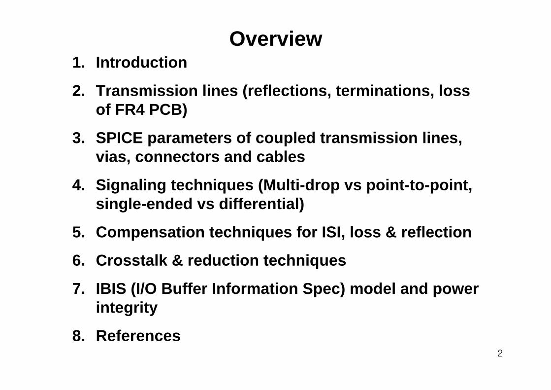
Overview1. Introduction
2. Transmission lines (reflections, terminations, loss of FR4 PCB)
3. SPICE parameters of coupled transmission lines, vias, connectors and cables
4. Signaling techniques (Multi-drop vs point-to-point, single-ended vs differential)
5. Compensation techniques for ISI, loss & reflection
6. Crosstalk & reduction techniques
7. IBIS (I/O Buffer Information Spec) model and power integrity
8. References

3
1. Introduction
4
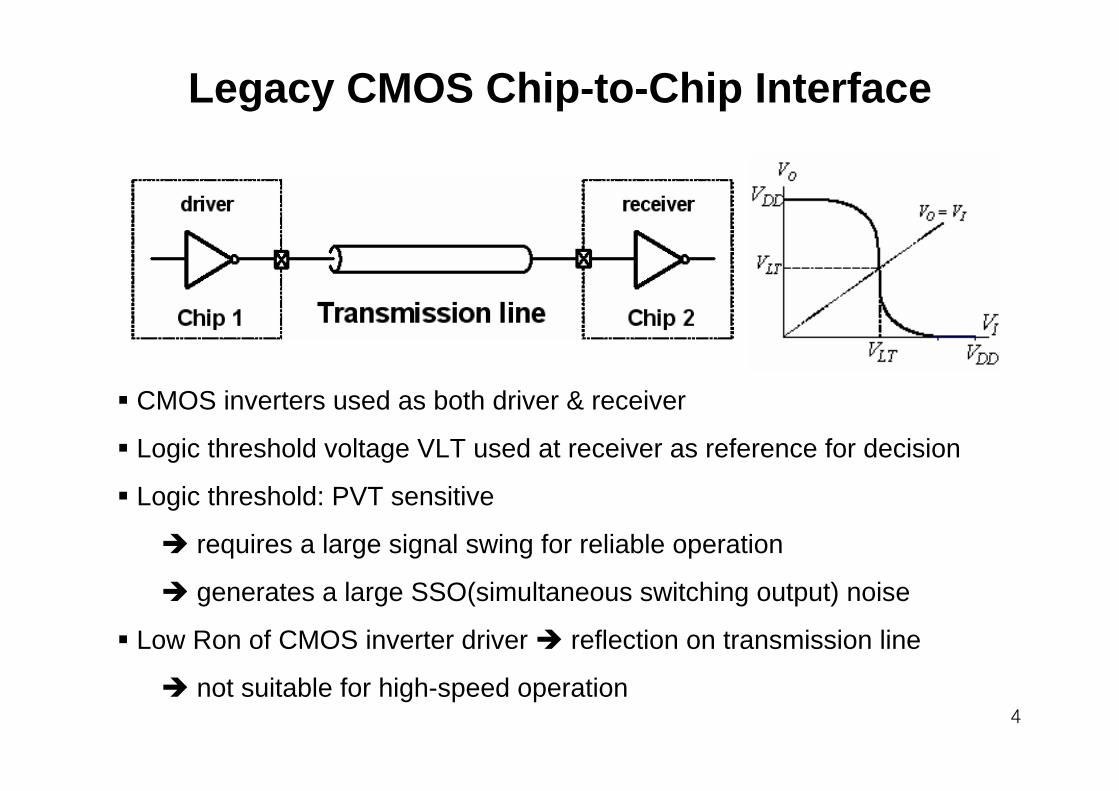
Legacy CMOS Chip-to-Chip Interface
CMOS inverters used as both driver & receiver
Logic threshold voltage VLT used at receiver as reference for decision
Logic threshold: PVT sensitive
requires a large signal swing for reliable operation
generates a large SSO(simultaneous switching output) noise
Low Ron of CMOS inverter driver reflection on transmission line
not suitable for high-speed operation
5
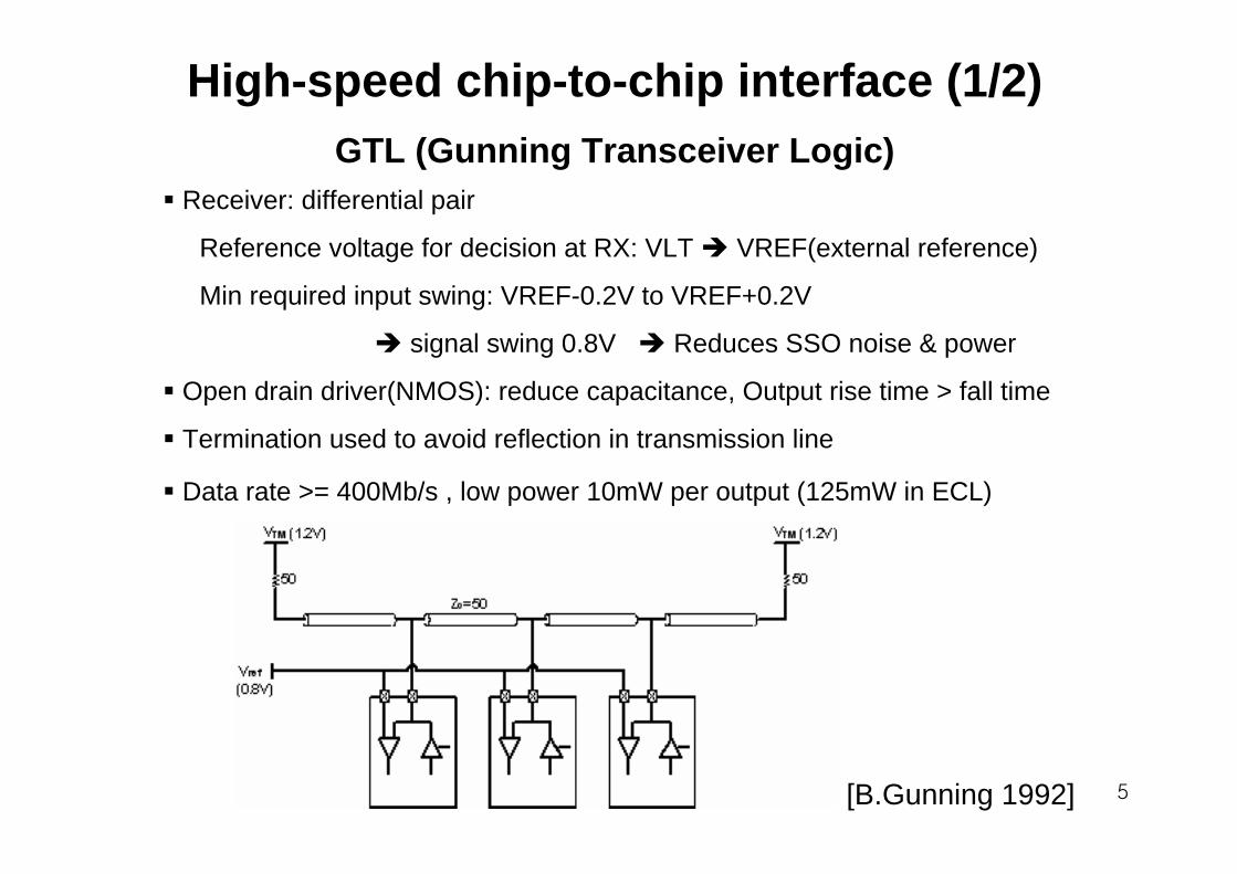
High-speed chip-to-chip interface (1/2)GTL (Gunning Transceiver Logic)
Receiver: differential pair
Reference voltage for decision at RX: VLT VREF(external reference)
Min required input swing: VREF-0.2V to VREF+0.2V
signal swing 0.8V Reduces SSO noise & power
Open drain driver(NMOS): reduce capacitance, Output rise time > fall time
Termination used to avoid reflection in transmission line
Data rate >= 400Mb/s , low power 10mW per output (125mW in ECL)
[B.Gunning 1992]
6
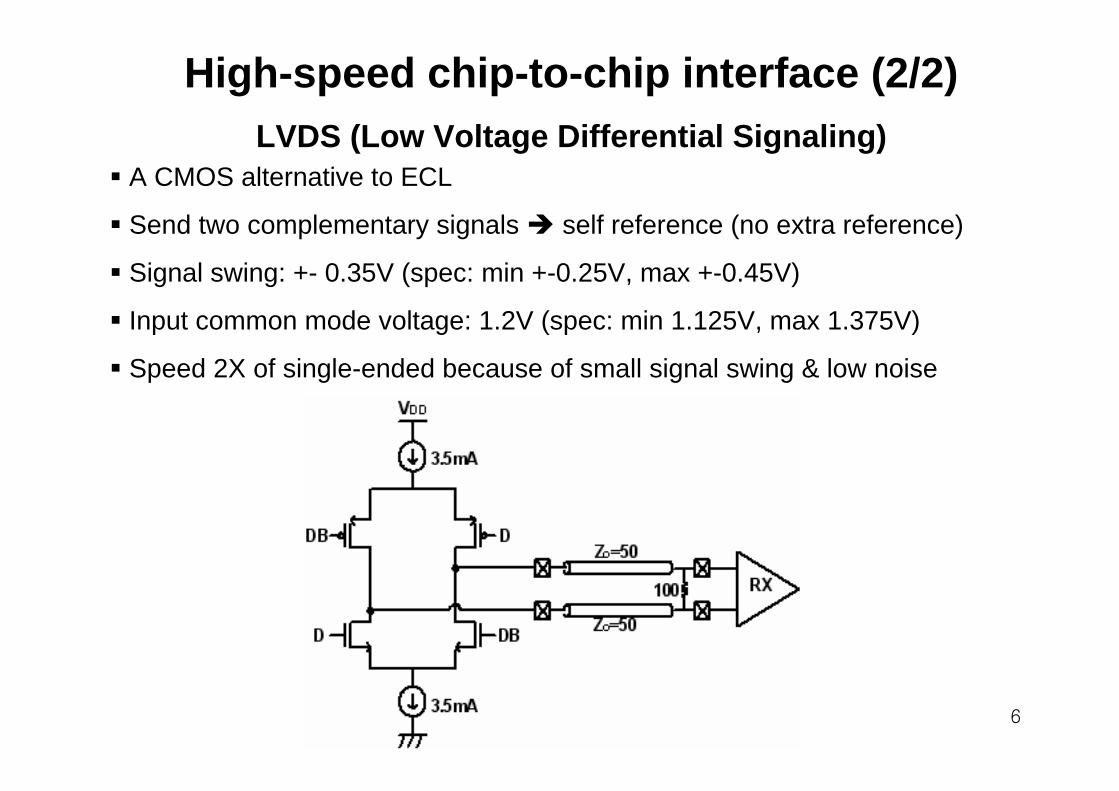
High-speed chip-to-chip interface (2/2)LVDS (Low Voltage Differential Signaling)
A CMOS alternative to ECL
Send two complementary signals self reference (no extra reference)
Signal swing: +- 0.35V (spec: min +-0.25V, max +-0.45V)
Input common mode voltage: 1.2V (spec: min 1.125V, max 1.375V)
Speed 2X of single-ended because of small signal swing & low noise
7
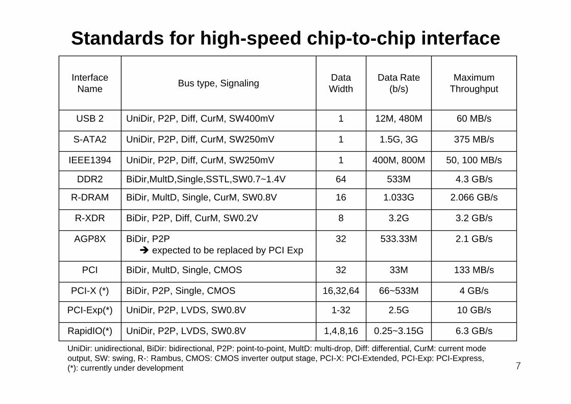
6.3 GB/s0.25~3.15G1,4,8,16UniDir, P2P, LVDS, SW0.8VRapidIO(*)
10 GB/s2.5G1-32UniDir, P2P, LVDS, SW0.8VPCI-Exp(*)
4 GB/s66~533M16,32,64BiDir, P2P, Single, CMOSPCI-X (*)
133 MB/s33M32BiDir, MultD, Single, CMOSPCI
2.1 GB/s533.33M32BiDir, P2P expected to be replaced by PCI Exp
AGP8X
3.2 GB/s3.2G8BiDir, P2P, Diff, CurM, SW0.2VR-XDR
2.066 GB/s1.033G16BiDir, MultD, Single, CurM, SW0.8VR-DRAM
4.3 GB/s533M64BiDir,MultD,Single,SSTL,SW0.7~1.4VDDR2
50, 100 MB/s400M, 800M1UniDir, P2P, Diff, CurM, SW250mVIEEE1394
375 MB/s1.5G, 3G1UniDir, P2P, Diff, CurM, SW250mVS-ATA2
60 MB/s12M, 480M1UniDir, P2P, Diff, CurM, SW400mVUSB 2
MaximumThroughput
Data Rate (b/s)
DataWidthBus type, SignalingInterface
Name
UniDir: unidirectional, BiDir: bidirectional, P2P: point-to-point, MultD: multi-drop, Diff: differential, CurM: current mode output, SW: swing, R-: Rambus, CMOS: CMOS inverter output stage, PCI-X: PCI-Extended, PCI-Exp: PCI-Express, (*): currently under development
Standards for high-speed chip-to-chip interface
8
2. Transmission lines
(reflections, terminations, loss of FR4 PCB)
9
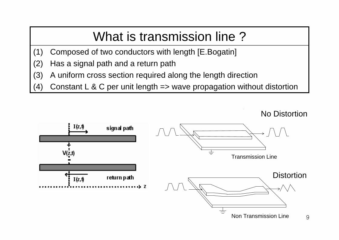
(1) Composed of two conductors with length [E.Bogatin](2) Has a signal path and a return path(3) A uniform cross section required along the length direction(4) Constant L & C per unit length => wave propagation without distortion
What is transmission line ?
No Distortion
Distortion
Transmission Line
Non Transmission Line
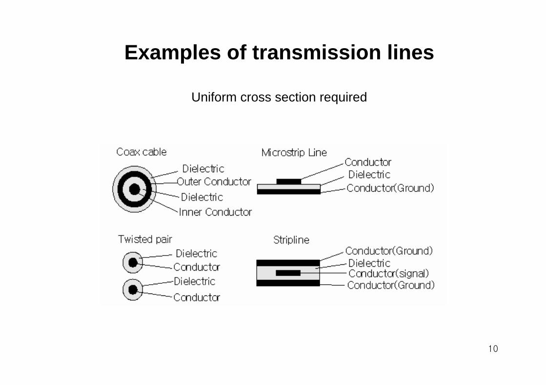
10
Examples of transmission lines
Uniform cross section required

11
If circuit size << wavelength of the highest freq. of signal
When can we use KCL & KVL analysis ?
∫∫ ⋅∂∂
−=⋅ dSBt
dLE
∫∫∫ ⋅−=++5
4
3
2
1
0)(tIL
dtdEdlEdlEdl
dttdIL
CtQtIRtVs
)()()()( ⋅++⋅=
Maxwell equations reduced to KCL, KVL
The loop current I(t) is the same at all locations of loop at a given time t
(KVL: Kirchhoff voltage law)
+
-
R
EI (t)
1
0
2 3 4 5
6
7
8
LVs (t)
C
I (t)
12
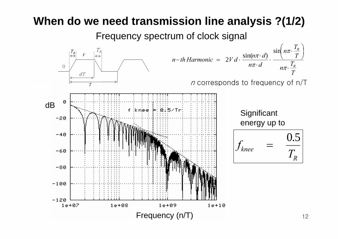
Frequency spectrum of clock signal
dB
Frequency (n/T)
TTn
TTn
dndndVHarmonicthn
R
R
⋅
⎟⎠⎞
⎜⎝⎛ ⋅
⋅⋅⋅
⋅=−π
π
ππ
sin)sin(2
Rknee T
f 5.0=
Significant energy up to
When do we need transmission line analysis ?(1/2)
V
0
TR
T
dT
TR
n corresponds to frequency of n/T
13
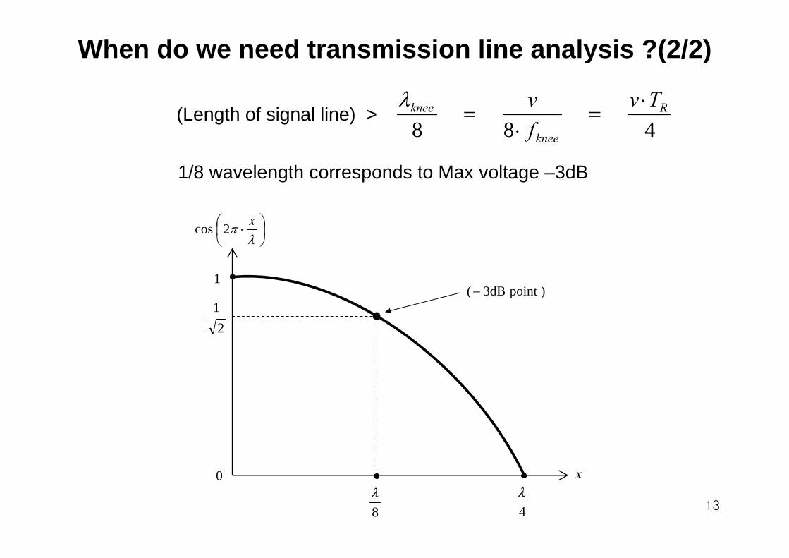
488R
knee
knee Tvfv ⋅
=⋅
=λ
(Length of signal line) >
1/8 wavelength corresponds to Max voltage –3dB
21
1
0
8λ
4λ
x
⎟⎠⎞
⎜⎝⎛ ⋅
λπ x2cos
)point3dB(−
When do we need transmission line analysis ?(2/2)
14
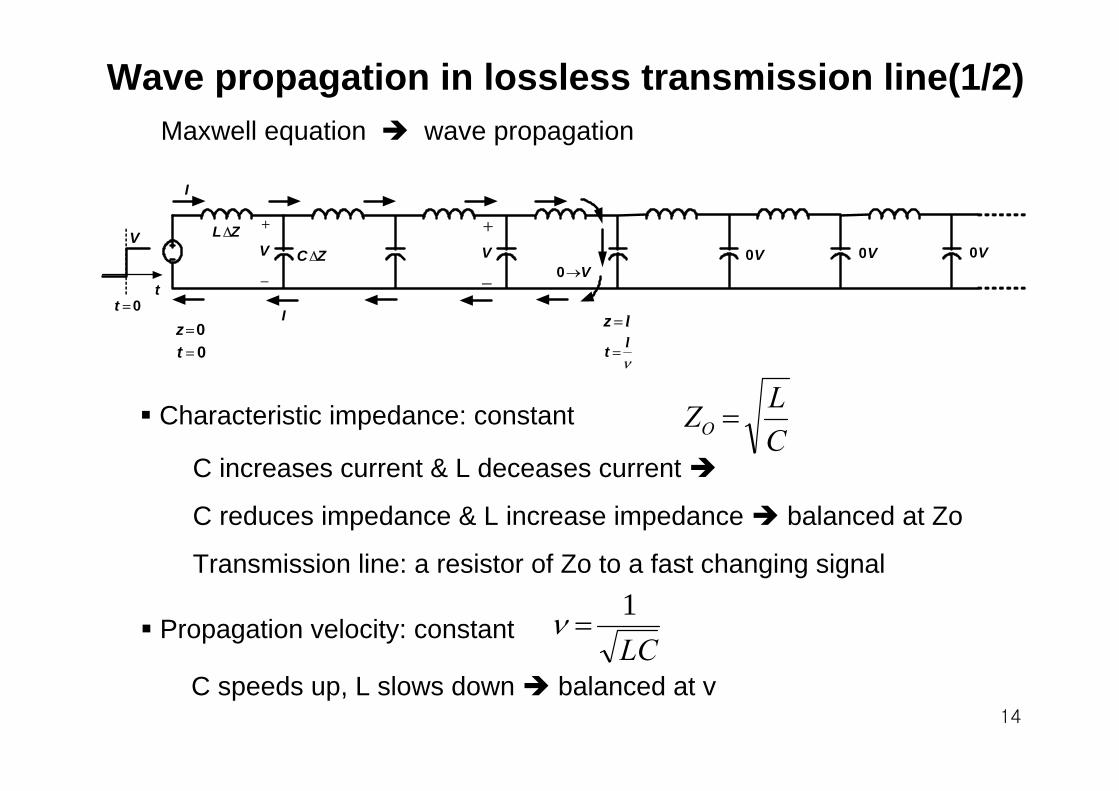
Wave propagation in lossless transmission line(1/2)
+
−
V ZC∆
ZL∆
I
V
t0=t
+
−
VV→0
V0 V0 V0
I0=z l=z
0=tνl
=t
Characteristic impedance: constantCLZO =
Propagation velocity: constantLC1
=ν
C increases current & L deceases current
C reduces impedance & L increase impedance balanced at Zo
Transmission line: a resistor of Zo to a fast changing signal
C speeds up, L slows down balanced at v
Maxwell equation wave propagation
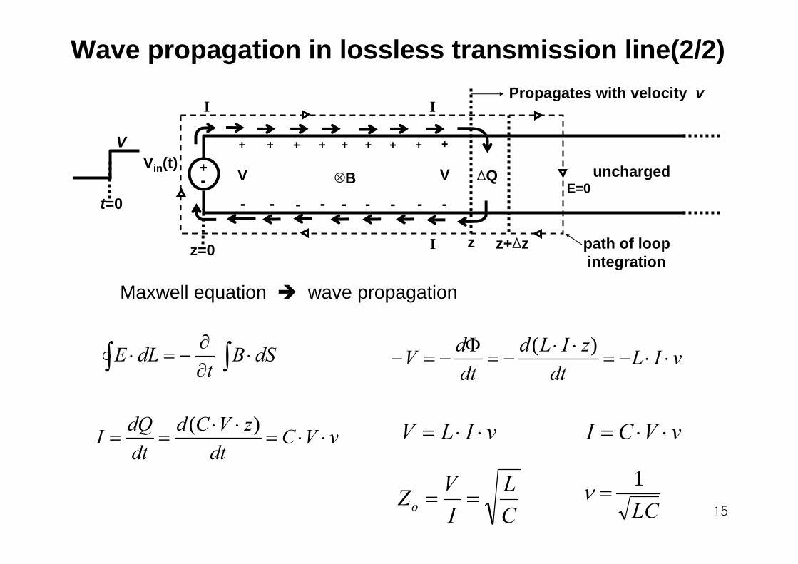
15
Wave propagation in lossless transmission line(2/2)
Maxwell equation wave propagation
∫∫ ⋅∂∂
−=⋅ dSBt
dLE vILdt
zILddtdV ⋅⋅−=
⋅⋅−=
Φ−=−
)(
vVCdt
zVCddtdQI ⋅⋅=
⋅⋅==
)(
CL
IVZo == LC
1=ν
vVCIvILV ⋅⋅=⋅⋅=
uncharged
+ + ++ + + + + +
- - - - - - - - -
path of loopintegration
t=0
z=0
I
+-
V
⊗V V
I
Vin(t)E=0
I z
Propagates with velocity v
z+∆z
∆QB
16
µ0, ε1
Exi
Hyi incident
µ0, ε2
Ext
Hyt transmitted
Exr
Hyr
reflected
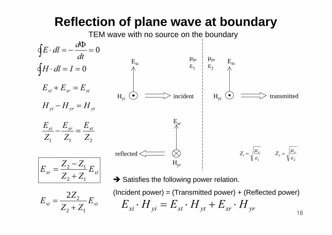
TEM wave with no source on the boundary
∫ =Φ
−=⋅ 0dtddlE
∫ ==⋅ 0IdlH
xtxrxi EEE =+
ytyryi HHH =−
Reflection of plane wave at boundary
xixr EZZZZE
12
12
+−
=Satisfies the following power relation.
(Incident power) = (Transmitted power) + (Reflected power)
yrxrytxtyixi HEHEHE ⋅+⋅=⋅
11 ε
µoZ =2
2 εµoZ =
211 ZE
ZE
ZE xtxrxi =−
xixt EZZ
ZE12
22+
=
17
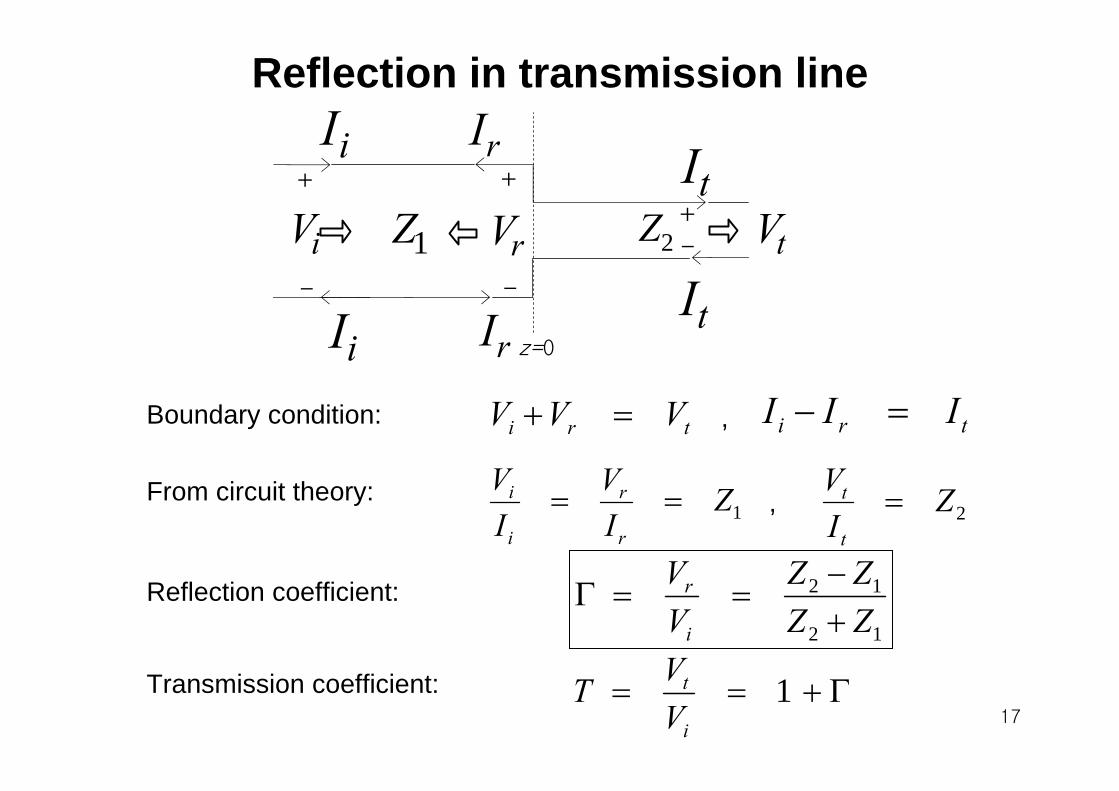
Reflection in transmission line
,
,
Reflection coefficient:12
12
ZZZZ
VV
i
r
+−
==Γ
tri VVV =+ tri III =−Boundary condition:
1ZIV
IV
r
r
i
i == 2ZIV
t
t =From circuit theory:
Γ+== 1i
t
VVTTransmission coefficient:
z=0
-
+
-
+
-
+
rI
iI
iV rV tV
iI
rI
tI
tI1Z 2Z
18
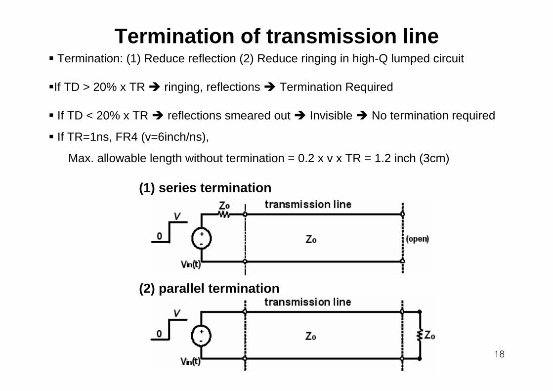
Termination: (1) Reduce reflection (2) Reduce ringing in high-Q lumped circuit
If TD > 20% x TR ringing, reflections Termination Required
If TD < 20% x TR reflections smeared out Invisible No termination required
If TR=1ns, FR4 (v=6inch/ns),
Max. allowable length without termination = 0.2 x v x TR = 1.2 inch (3cm)
Termination of transmission line
(1) series termination
(2) parallel termination
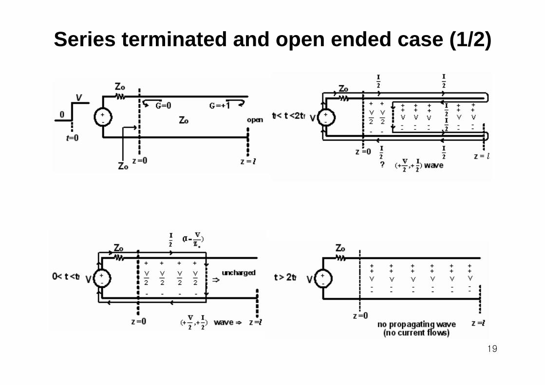
19
Series terminated and open ended case (1/2)
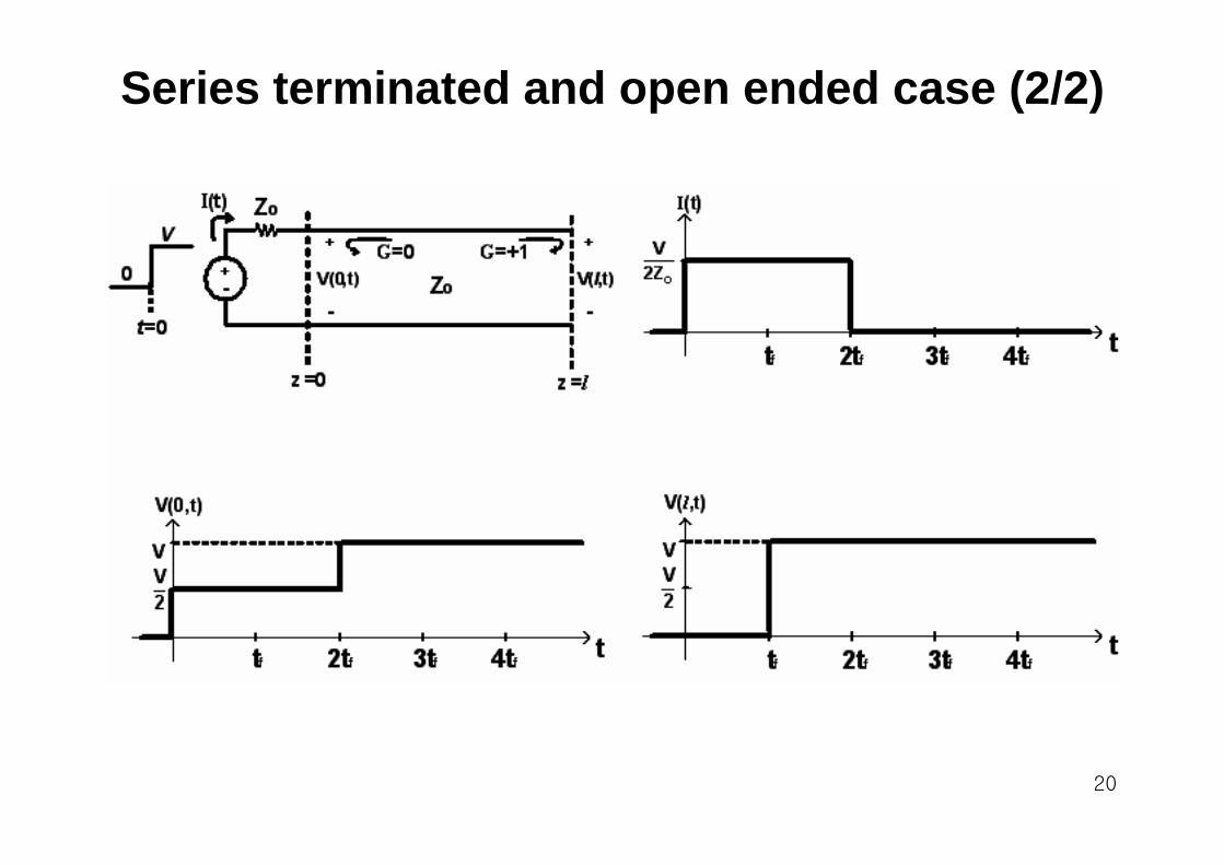
20
Series terminated and open ended case (2/2)
21
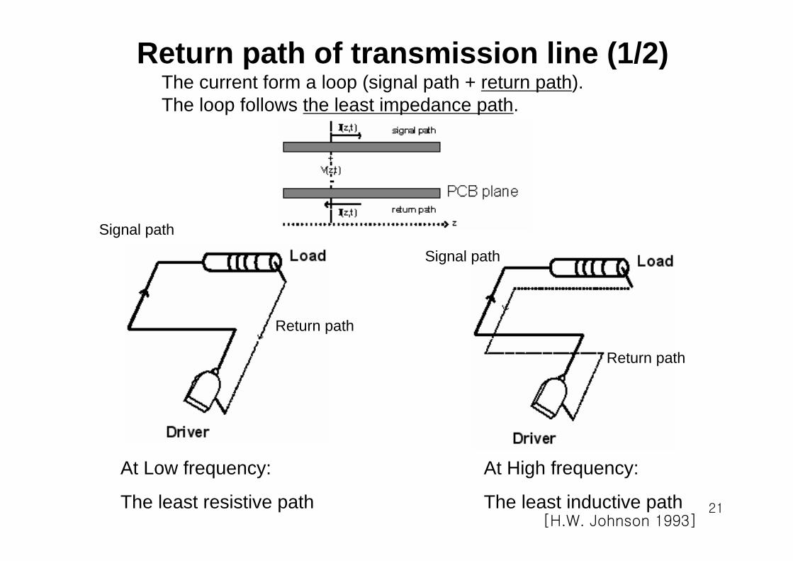
Return path of transmission line (1/2)The current form a loop (signal path + return path).The loop follows the least impedance path.
At Low frequency:
The least resistive path
At High frequency:
The least inductive path[H.W. Johnson 1993]
Signal path
Return path
Return path
Signal path
22
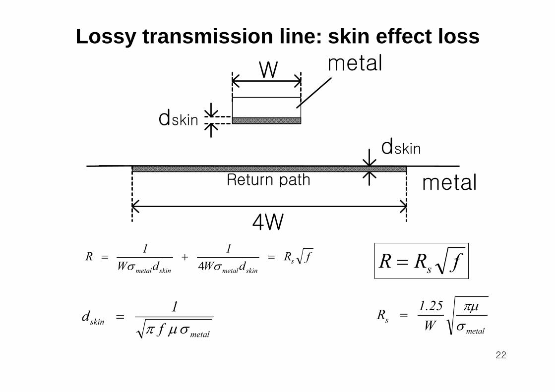
Lossy transmission line: skin effect loss
metalskin f
1 dσµπ
=
fR dW
1 dW
1 R sskinmetalskinmetal
=+=σσ 4
metals W
1.25 Rσπµ
=
W
4W
metal
dskin
dskin
metal
Return path
fRR s=
23
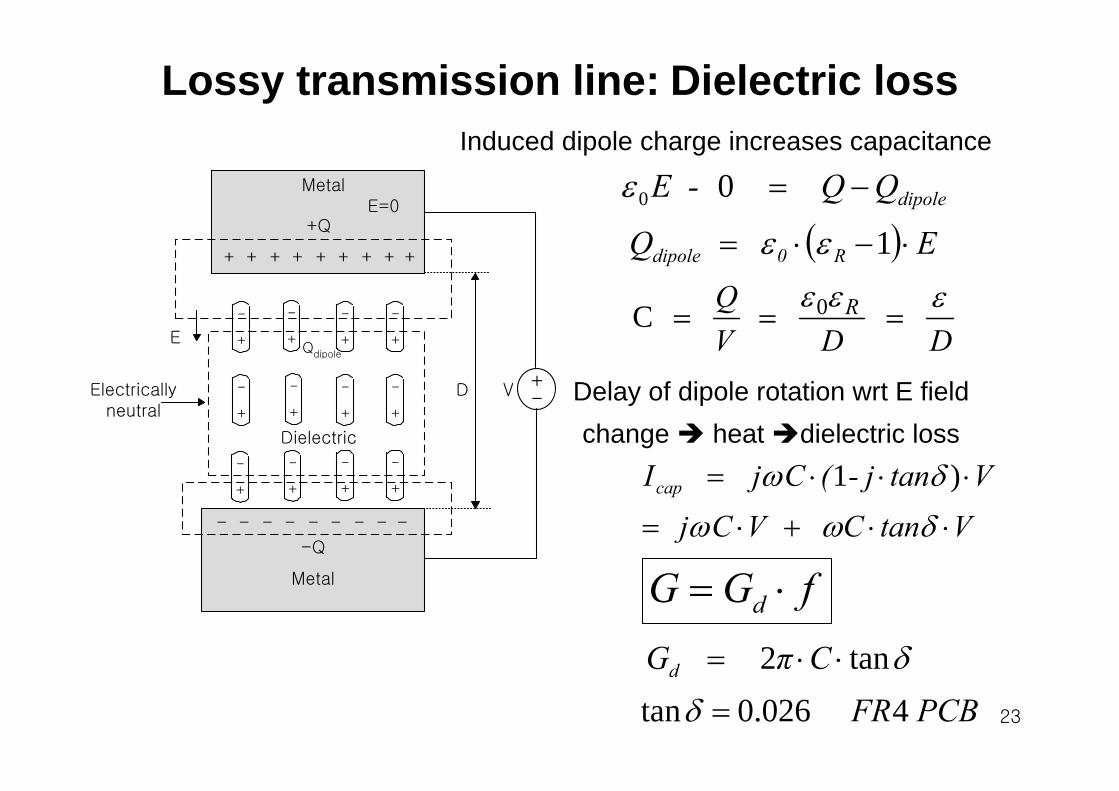
Metal
+-
-
+
-
+
-
+
-
+
-
+
-
+
-
+
-
+
-
+
-
+
-
+
-
+
+ + + + + + + + +
- - - - - - - - -
+QE=0
Qdipole
E
Electricallyneutral
D V
-Q
Metal
Dielectric
Lossy transmission line: Dielectric loss
dipoleQ Q E - −=00ε
( ) E Q R0dipole ⋅−⋅= 1εε
DD
VQ R εεε
C 0 ===
VtanC VCj
Vtanj-(Cj Icap
⋅⋅+⋅=
⋅⋅⋅=
δωω
δω )1
δtan2 ⋅⋅= Cπ Gd
PCBFR4026.0tan =δ
fGG d ⋅=
Induced dipole charge increases capacitance
Delay of dipole rotation wrt E field change heat dielectric loss
24
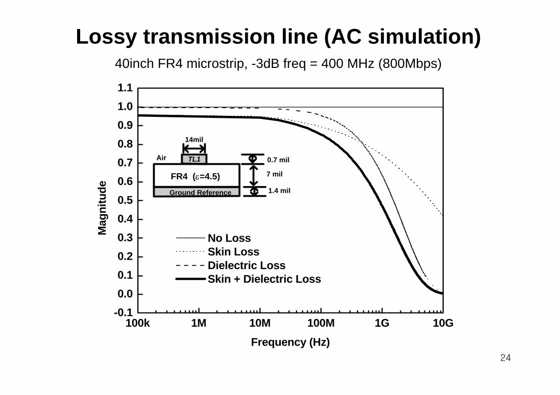
Lossy transmission line (AC simulation)
0.7 mil
7 mil
1.4 mil
Air
FR4 (ε=4.5)
14mil
TL1
Ground Reference
40inch FR4 microstrip, -3dB freq = 400 MHz (800Mbps)
100k 1M 10M 100M 1G 10G-0.10.00.10.20.30.40.50.60.70.80.91.01.1
Mag
nitu
de
Frequency (Hz)
No Loss Skin Loss Dielectric Loss Skin + Dielectric Loss
25
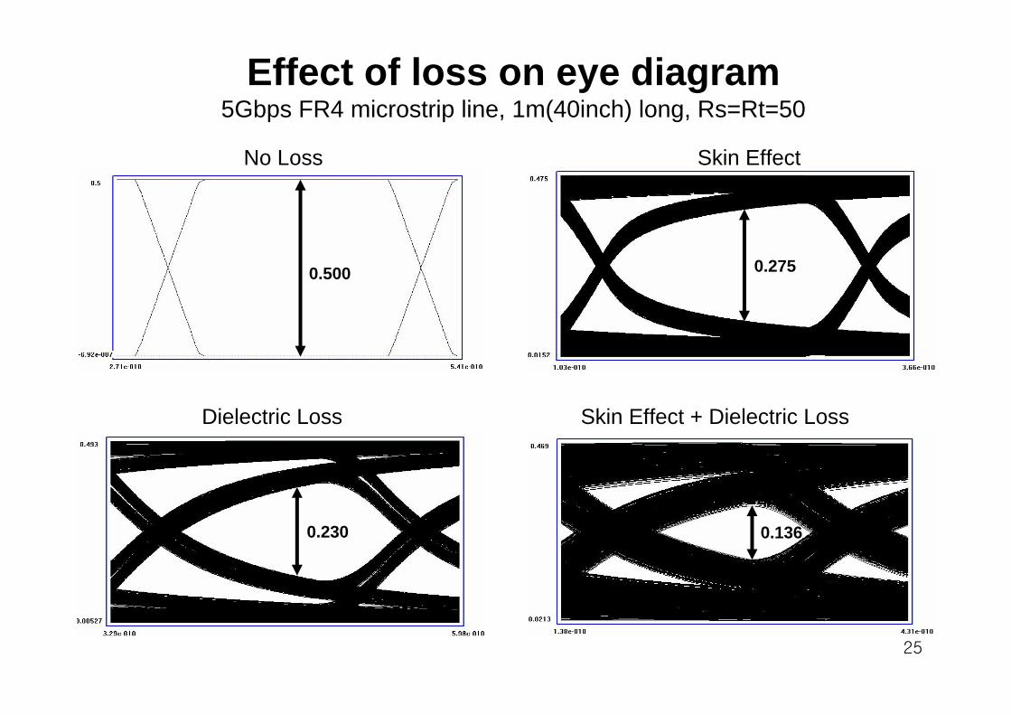
Effect of loss on eye diagram5Gbps FR4 microstrip line, 1m(40inch) long, Rs=Rt=50
No Loss
0.500
0.136
Skin Effect + Dielectric LossDielectric Loss
0.230
Skin Effect
0.275
26
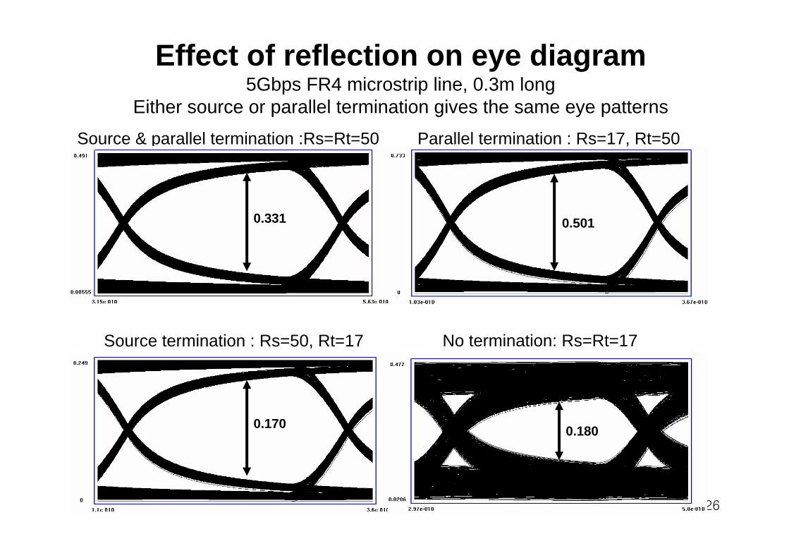
Effect of reflection on eye diagram5Gbps FR4 microstrip line, 0.3m long
Either source or parallel termination gives the same eye patterns
No termination: Rs=Rt=17
0.180
Source termination : Rs=50, Rt=17
Source & parallel termination :Rs=Rt=50
0.331
Parallel termination : Rs=17, Rt=50
0.501
0.170
27
3. SPICE parameters of
coupled transmission lines,
vias,
connectors,
& cables
28
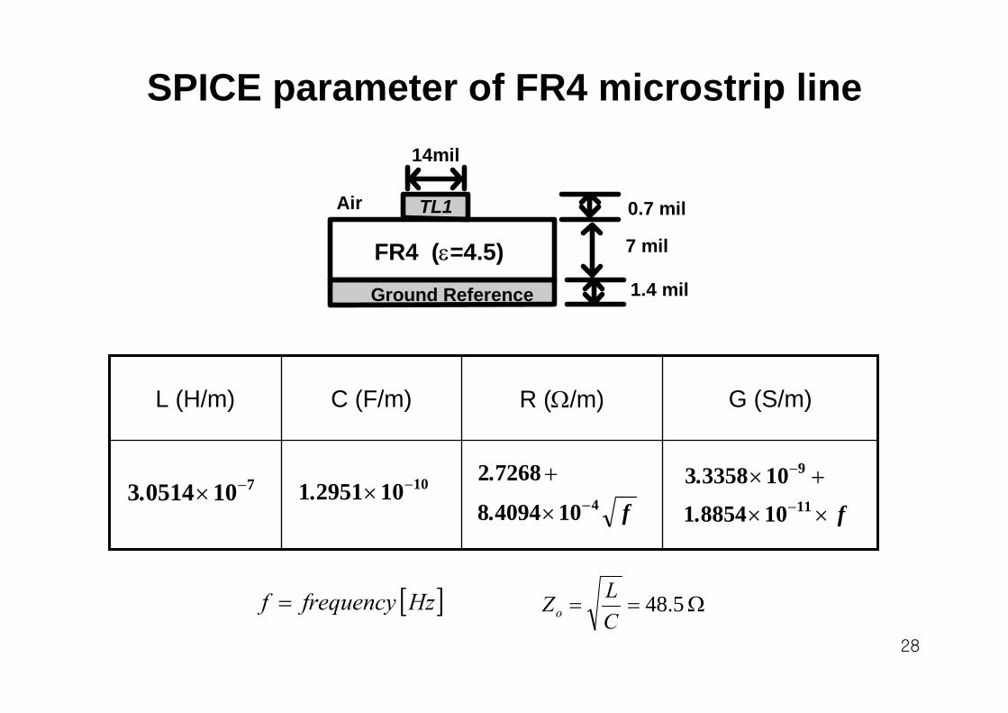
SPICE parameter of FR4 microstrip line
G (S/m)R (Ω/m)C (F/m)L (H/m)
0.7 mil
7 mil
1.4 mil
Air
FR4 (ε=4.5)
14mil
TL1
Ground Reference
71005143 −×. 101029511 −×.f.
.41040948
72682−×
+
f.
.
××
+×−
−
11
9
1088541
1033583
[ ]Hzfrequencyf = Ω== 5.48CLZo
29
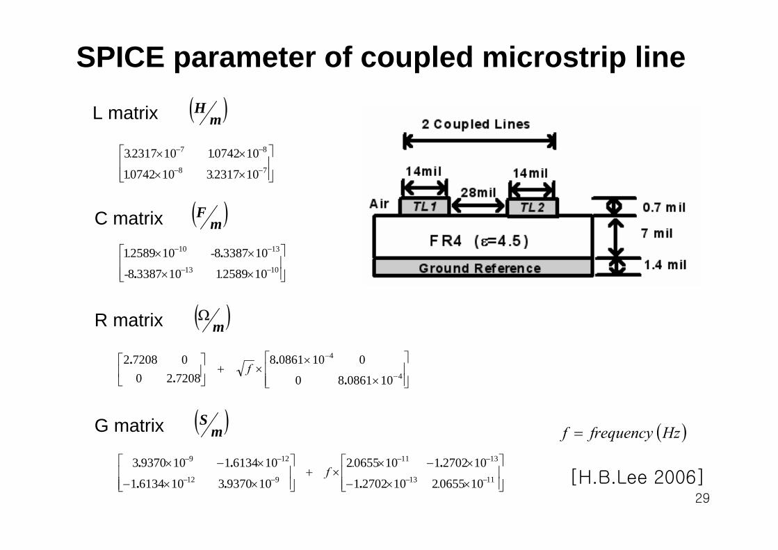
SPICE parameter of coupled microstrip line
L matrix ( )mH
⎥⎥⎦
⎤
⎢⎢⎣
⎡
××
××−−
−−
78
87
10231731007421
10074211023173
..
..
⎥⎥⎦
⎤
⎢⎢⎣
⎡
××
××−−
−−
1013
1310
10258911033878
10338781025891
.-
-.
.
.
C matrix ( )mF
R matrix
⎥⎥⎦
⎤
⎢⎢⎣
⎡
×
××+⎥
⎦
⎤⎢⎣
⎡−
−
4
4
10086180
01008618720820072082
.
..
.f
( )mΩ
( )Hzfrequencyf =G matrix
⎥⎥⎦
⎤
⎢⎢⎣
⎡
××−
×−××+
⎥⎥⎦
⎤
⎢⎢⎣
⎡
××−
×−×−−
−−
−−
−−
1113
1311
912
129
10065521027021
10270211006552
10937031061341
10613411093703
.
.f
.
.
..
..
( )mS
[H.B.Lee 2006]
30
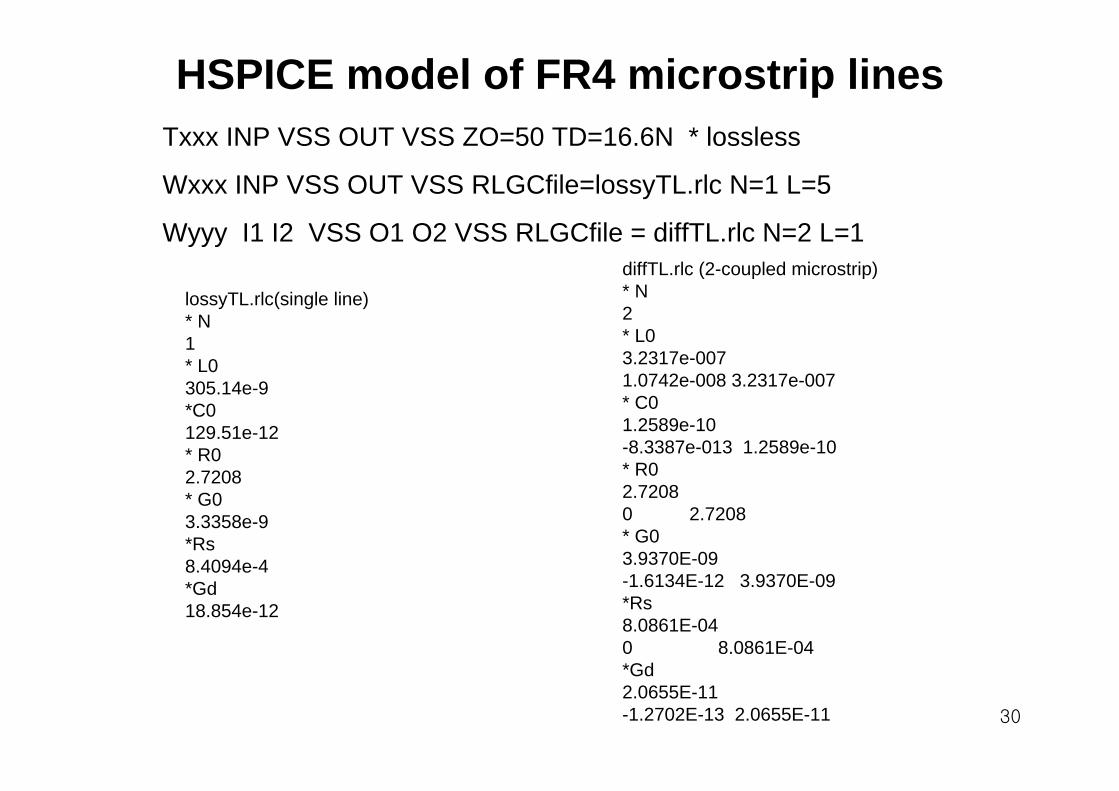
lossyTL.rlc(single line)* N1* L0305.14e-9 *C0129.51e-12* R02.7208* G03.3358e-9*Rs8.4094e-4*Gd18.854e-12
Txxx INP VSS OUT VSS ZO=50 TD=16.6N * lossless
Wxxx INP VSS OUT VSS RLGCfile=lossyTL.rlc N=1 L=5
Wyyy I1 I2 VSS O1 O2 VSS RLGCfile = diffTL.rlc N=2 L=1
HSPICE model of FR4 microstrip lines
diffTL.rlc (2-coupled microstrip)* N2* L03.2317e-0071.0742e-008 3.2317e-007* C01.2589e-10-8.3387e-013 1.2589e-10* R02.72080 2.7208* G03.9370E-09-1.6134E-12 3.9370E-09*Rs8.0861E-040 8.0861E-04*Gd2.0655E-11-1.2702E-13 2.0655E-11
31
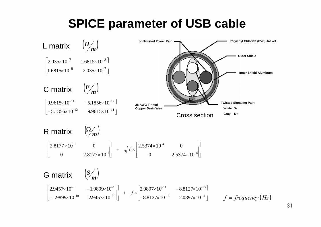
SPICE parameter of USB cableL matrix ( )m
H
⎥⎥⎦
⎤
⎢⎢⎣
⎡
××
××−−
−−
78
87
10035.2106815.1
106815.110035.2
⎥⎥⎦
⎤
⎢⎢⎣
⎡
××−
×−×−−
−−
1112
1211
10961591018565
10185651096159
..
..
C matrix ( )mF
R matrix
⎥⎥⎦
⎤
⎢⎢⎣
⎡
×
××+
⎥⎥⎦
⎤
⎢⎢⎣
⎡
×
×4-
-4
1-
-1
105374.20
0105374.2
102.81770
0102.8177f
( )mΩ
( )Hzfrequencyf =
G matrix
⎥⎥⎦
⎤
⎢⎢⎣
⎡
××−
×−××+
⎥⎥⎦
⎤
⎢⎢⎣
⎡
××−
×−×−−
−−
−−
−−
1113
1311
910
109
10089721081278
10812781008972
10945721098991
10989911094572
..
..
..
..f
( )mS
on-Twisted Power Pair Polyvinyl Chloride (PVC) Jacket
Outer Shield
Inner Shield Aluminum
28 AWG Tinned Copper Drain Wire
Twisted Signaling Pair:
White: D-
Gray: D+Cross section
32
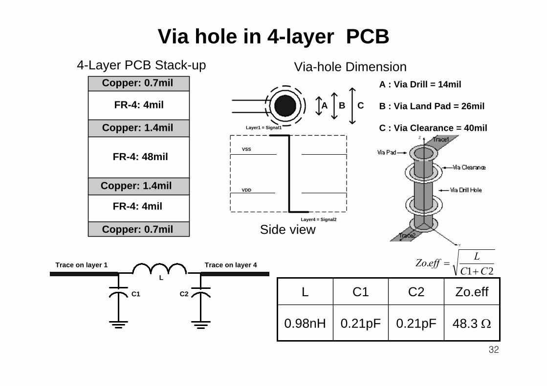
Via hole in 4-layer PCB
Copper: 0.7mil
FR-4: 4mil
Copper: 1.4mil
Copper: 1.4mil
Copper: 0.7mil
FR-4: 4mil
FR-4: 48mil
A B C
A : Via Drill = 14mil
B : Via Land Pad = 26mil
C : Via Clearance = 40mil
4-Layer PCB Stack-up Via-hole Dimension
Side view
C1 C2
L
Trace on layer 1 Trace on layer 4
0.21pF
C1
48.3 Ω0.21pF0.98nH
Zo.effC2L
VSS
VDD
Layer1 = Signal1
Layer4 = Signal2
21.
CCLeffZo+
=
33
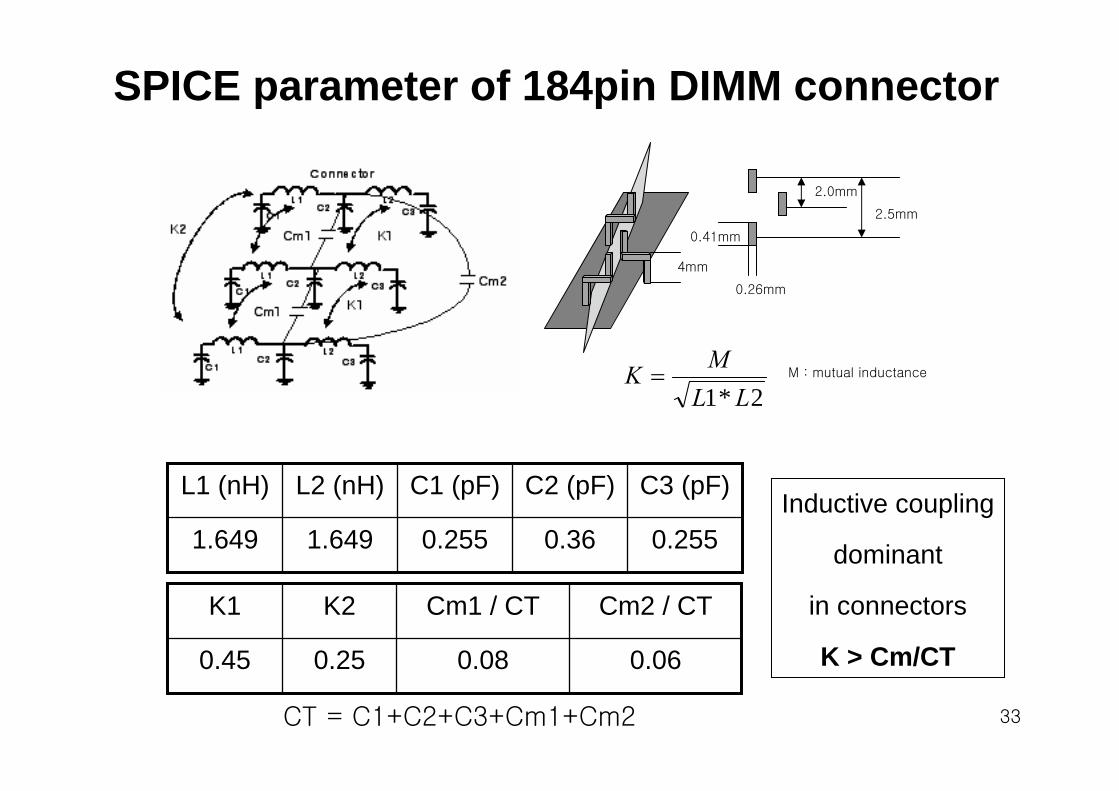
SPICE parameter of 184pin DIMM connector
0.2550.360.2551.6491.649
C3 (pF)C2 (pF)C1 (pF)L2 (nH)L1 (nH)
0.08
Cm1 / CT
0.06 0.250.45
Cm2 / CTK2K1
2*1 LLMK = M : mutual inductance
4mm
2.5mm
2.0mm
0.41mm
0.26mm
Inductive coupling
dominant
in connectors
K > Cm/CT
CT = C1+C2+C3+Cm1+Cm2
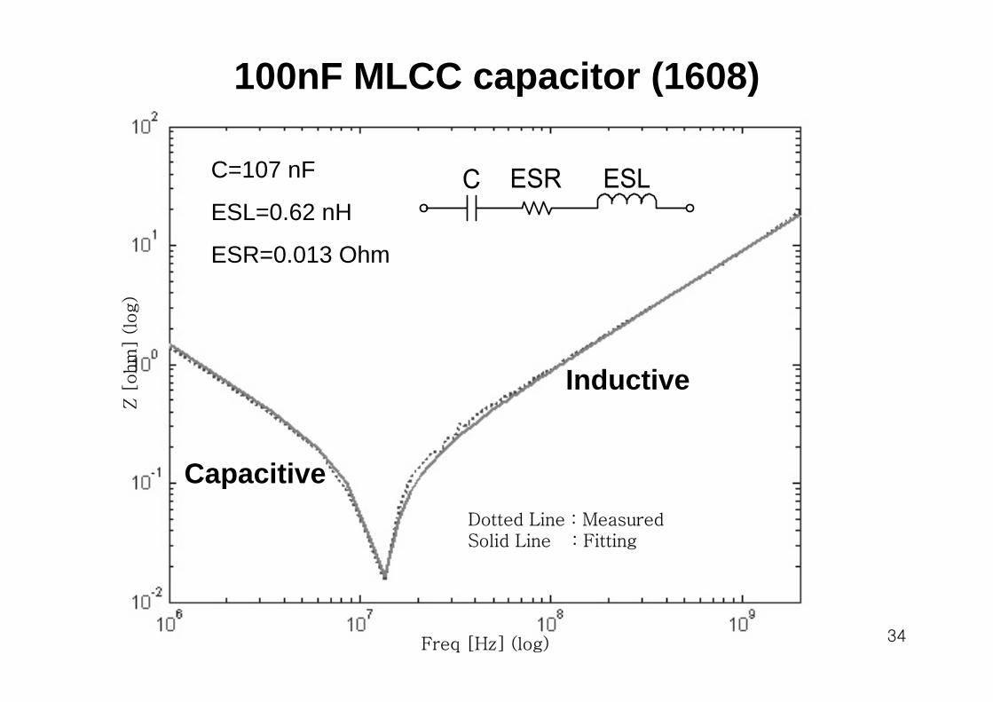
34Freq [Hz] (log)
Z [
ohm
] (log)
Dotted Line : MeasuredSolid Line ...: Fitting
C=107 nF
ESL=0.62 nH
ESR=0.013 Ohm
100nF MLCC capacitor (1608)
Inductive
Capacitive
35
4. Signaling techniques
(Multi-drop vs point-to-point,
single-ended vs differential)
36
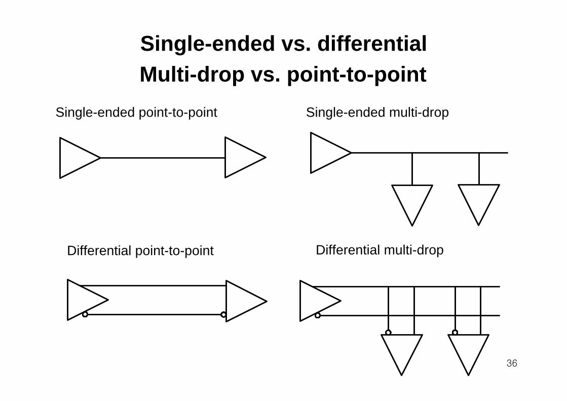
Single-ended vs. differential
Single-ended multi-drop
Differential multi-drop
Single-ended point-to-point
Differential point-to-point
Multi-drop vs. point-to-point
37
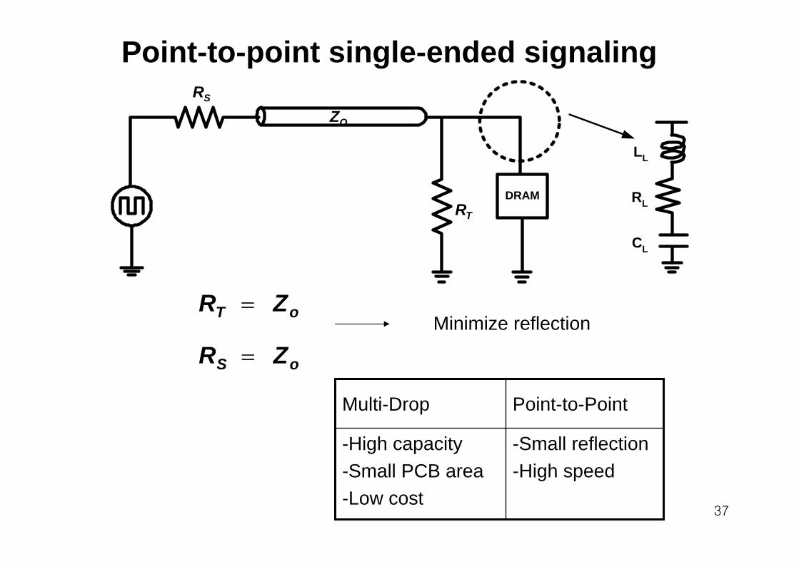
DRAMTR
SR
OZ
LL
RL
CL
oT ZR =Minimize reflection
oS ZR =
Point-to-point single-ended signaling
-Small reflection-High speed
-High capacity-Small PCB area-Low cost
Point-to-PointMulti-Drop
38
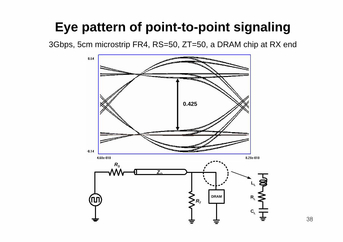
Eye pattern of point-to-point signaling3Gbps, 5cm microstrip FR4, RS=50, ZT=50, a DRAM chip at RX end
0.425
DRAMTR
SR
OZ
LL
RL
CL
39
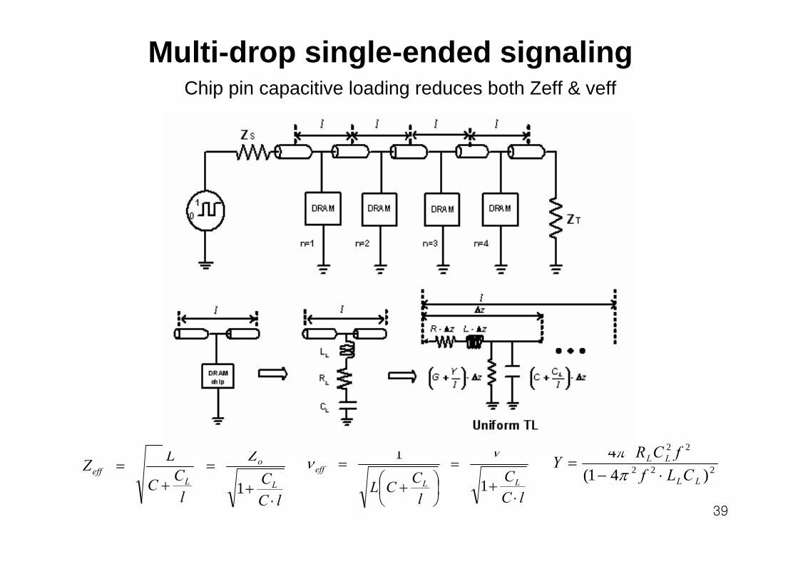
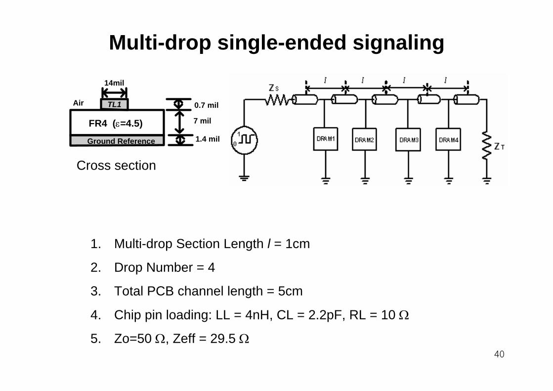
Multi-drop single-ended signalingChip pin capacitive loading reduces both Zeff & veff
222
222
)41(4
LL
LL
CLffCRY
⋅−=
ππ
lCC
Z
lCC
L ZL
o
Leff
⋅+
=+
=1 lC
Cv
lCCL
LL
eff
⋅+
=
⎟⎠⎞
⎜⎝⎛ +
=1
1ν
40
Multi-drop single-ended signaling
0.7 mil
7 mil
1.4 mil
Air
FR4 (ε=4.5)
14mil
TL1
Ground Reference
Cross section
1. Multi-drop Section Length l = 1cm
2. Drop Number = 4
3. Total PCB channel length = 5cm
4. Chip pin loading: LL = 4nH, CL = 2.2pF, RL = 10 Ω
5. Zo=50 Ω, Zeff = 29.5 Ω
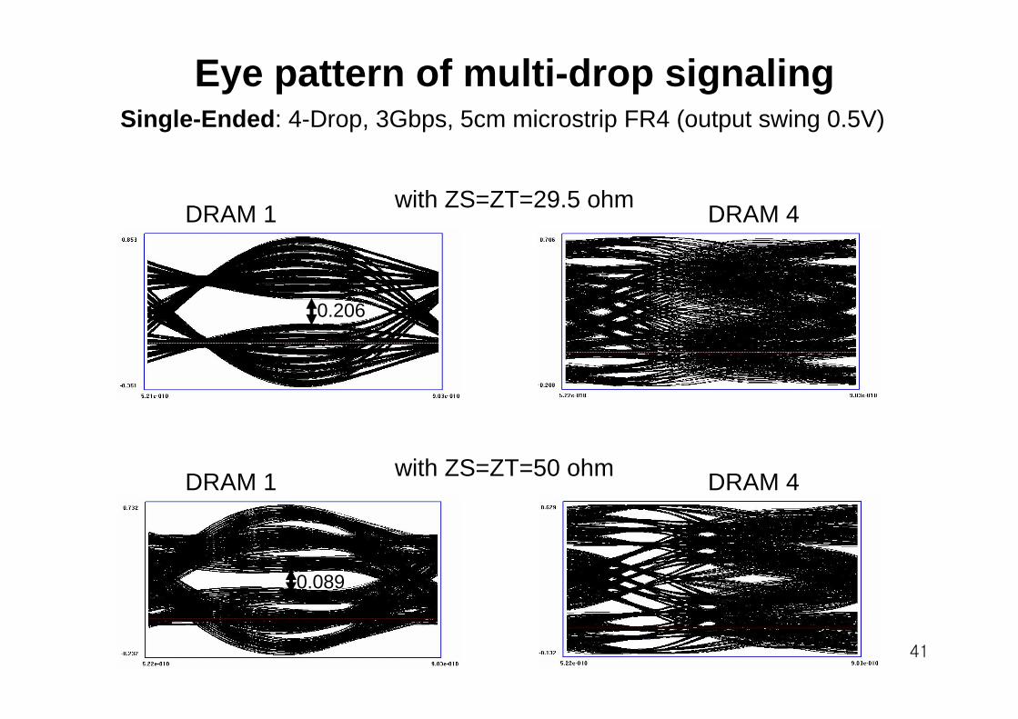
41
DRAM 1 DRAM 4with ZS=ZT=29.5 ohm
with ZS=ZT=50 ohmDRAM 1 DRAM 4
Single-Ended: 4-Drop, 3Gbps, 5cm microstrip FR4 (output swing 0.5V)
0.206
0.089
Eye pattern of multi-drop signaling
0.206
42
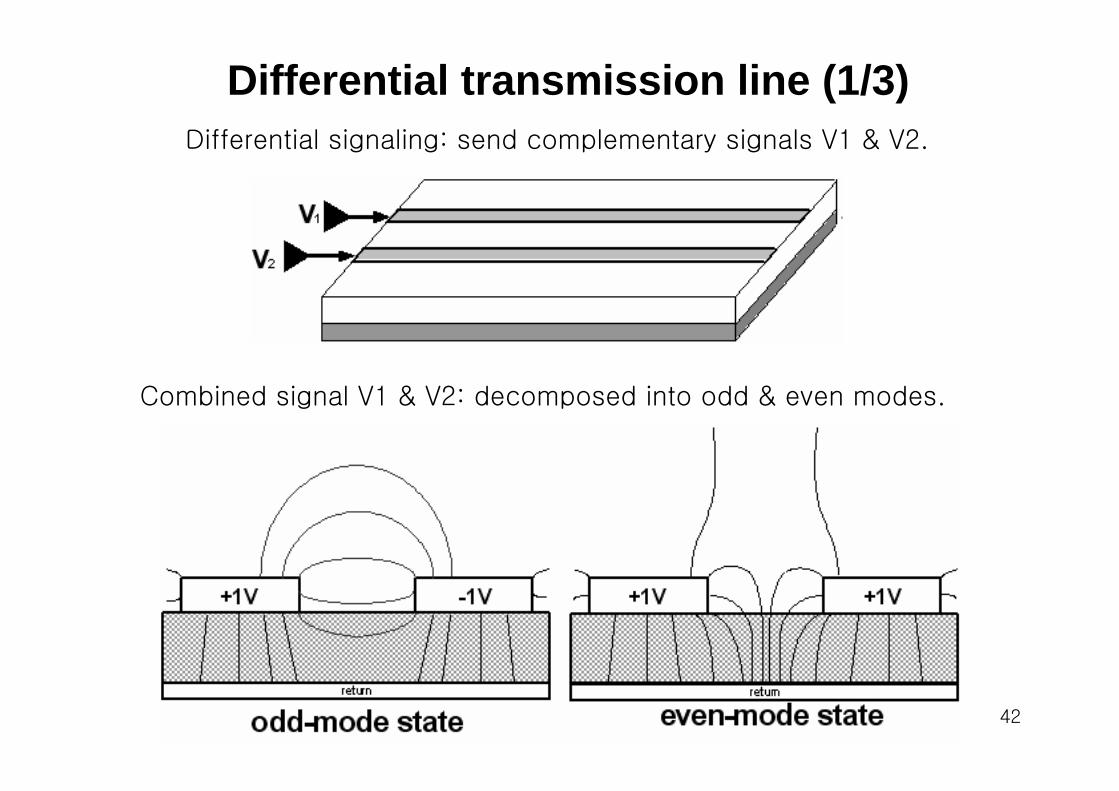
Differential transmission line (1/3)Differential signaling: send complementary signals V1 & V2.
Combined signal V1 & V2: decomposed into odd & even modes.
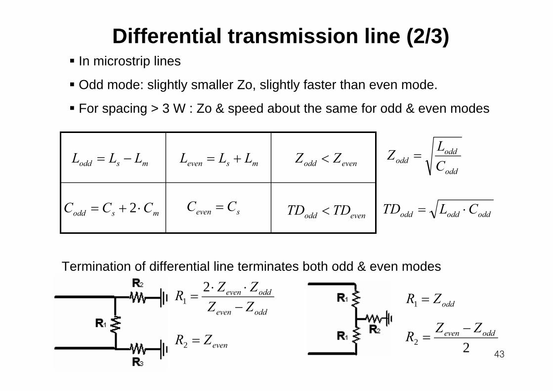
43
msodd LLL −=
msodd CCC ⋅+= 2
mseven LLL +=
seven CC =
evenodd ZZ <
evenodd TDTD <
odd
oddodd C
LZ =
oddoddodd CLTD ⋅=
In microstrip lines
Odd mode: slightly smaller Zo, slightly faster than even mode.
For spacing > 3 W : Zo & speed about the same for odd & even modes
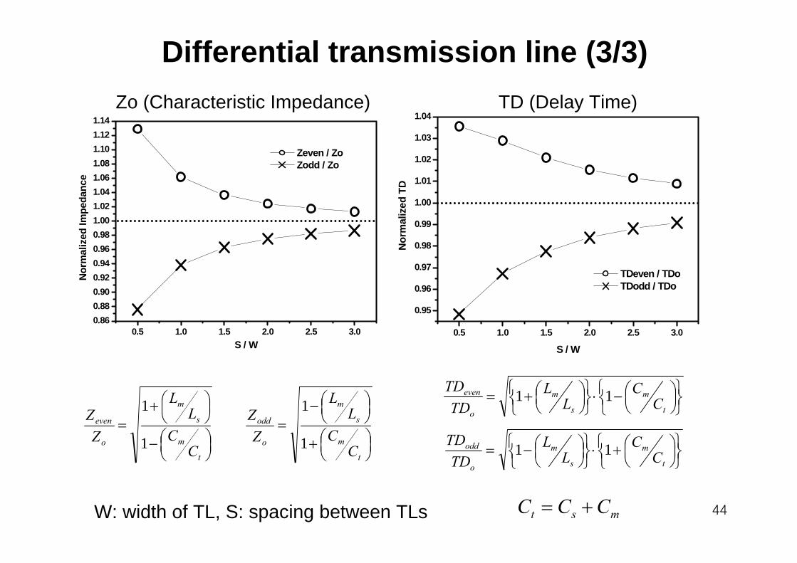
Differential transmission line (2/3)
Termination of differential line terminates both odd & even modes
oddeven
oddeven
ZZZZR
−⋅⋅
=2
1
evenZR =2
oddZR =1
22oddeven ZZR −
=
44
0.5 1.0 1.5 2.0 2.5 3.00.860.880.900.920.940.960.981.001.021.041.061.081.101.121.14
Nor
mal
ized
Impe
danc
e
S / W
Zeven / Zo Zodd / Zo
0.5 1.0 1.5 2.0 2.5 3.0
0.95
0.96
0.97
0.98
0.99
1.00
1.01
1.02
1.03
1.04
Nor
mal
ized
TD
S / W
TDeven / TDo TDodd / TDo
Differential transmission line (3/3)Zo (Characteristic Impedance) TD (Delay Time)
W: width of TL, S: spacing between TLs
⎟⎠⎞⎜
⎝⎛−
⎟⎠⎞⎜
⎝⎛+
=
t
m
s
m
o
even
CC
LL
ZZ
1
1
⎟⎠⎞⎜
⎝⎛+
⎟⎠⎞⎜
⎝⎛−
=
t
m
s
m
o
odd
CC
LL
ZZ
1
1 ⎭⎬⎫
⎩⎨⎧
⎟⎠⎞⎜
⎝⎛−⋅
⎭⎬⎫
⎩⎨⎧
⎟⎠⎞⎜
⎝⎛+=
t
m
s
m
o
evenC
CL
LTD
TD 11
⎭⎬⎫
⎩⎨⎧
⎟⎠⎞⎜
⎝⎛+⋅
⎭⎬⎫
⎩⎨⎧
⎟⎠⎞⎜
⎝⎛−=
t
m
s
m
o
oddC
CL
LTD
TD 11
mst CCC +=

45
5. Compensation techniques for
ISI, loss & reflection
46
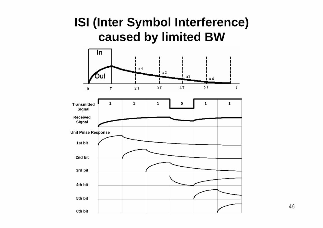
ISI (Inter Symbol Interference)caused by limited BW
TransmittedSIgnal
ReceivedSIgnal
Unit Pulse Response
1 1 1 0 1 1
1st bit
2nd bit
3rd bit
4th bit
5th bit
6th bit
47
HH
HL
LH
LL
0 1 1 1 0 0
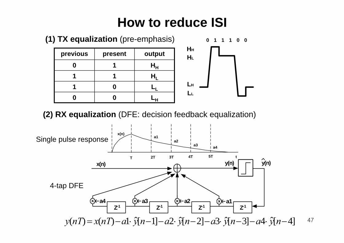
How to reduce ISI
LH00LL01HL11HH10
outputpresentprevious
(1) TX equalization (pre-emphasis)
Z-1 Z-1
x(n)
Z-1Z-1a1a2a3a4
y(n) y(n)
x(n)
T 2T 3T t
a1a2
4T 5T
a3 a4
]4[ˆ4]3[ˆ3]2[ˆ2]1[ˆ1)()( −⋅−−⋅−−⋅−−⋅−= nyanyanyanyanTxnTy
(2) RX equalization (DFE: decision feedback equalization)
Single pulse response
4-tap DFE
48
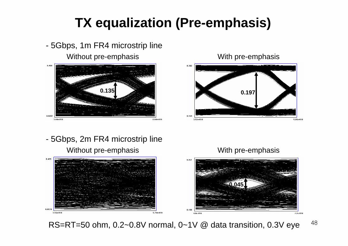
TX equalization (Pre-emphasis)- 5Gbps, 1m FR4 microstrip line
Without pre-emphasis With pre-emphasis
- 5Gbps, 2m FR4 microstrip lineWithout pre-emphasis With pre-emphasis
0.135 0.197
0.045
RS=RT=50 ohm, 0.2~0.8V normal, 0~1V @ data transition, 0.3V eye
49
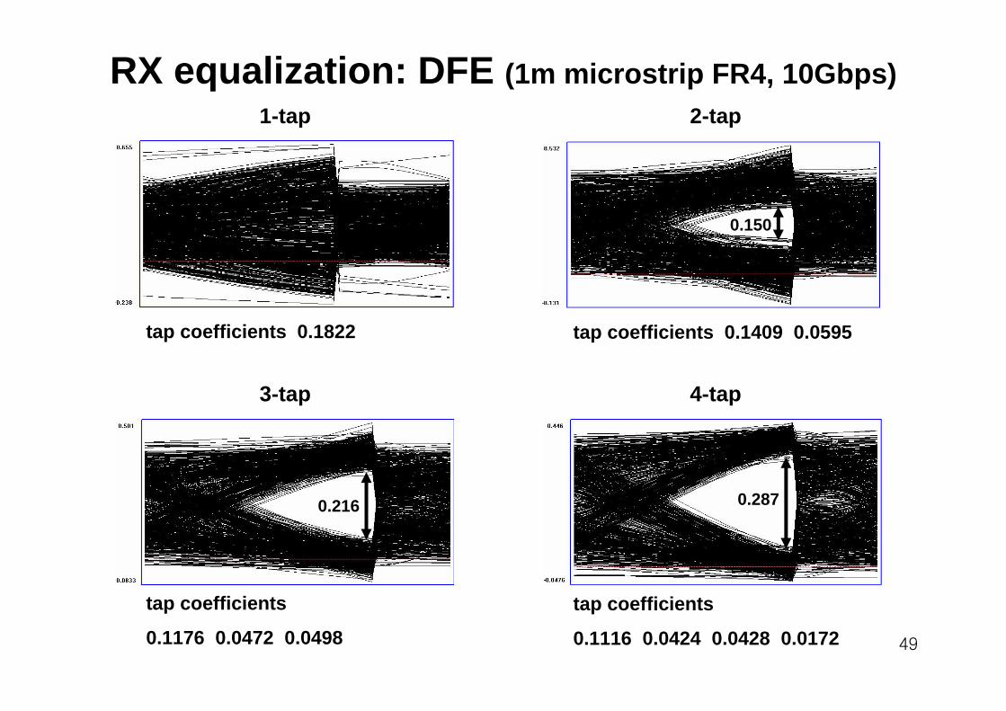
RX equalization: DFE (1m microstrip FR4, 10Gbps)1-tap 2-tap
tap coefficients 0.1822 tap coefficients 0.1409 0.0595
0.150
3-tap 4-tap
tap coefficients
0.1176 0.0472 0.0498
tap coefficients
0.1116 0.0424 0.0428 0.0172
0.216 0.287
50
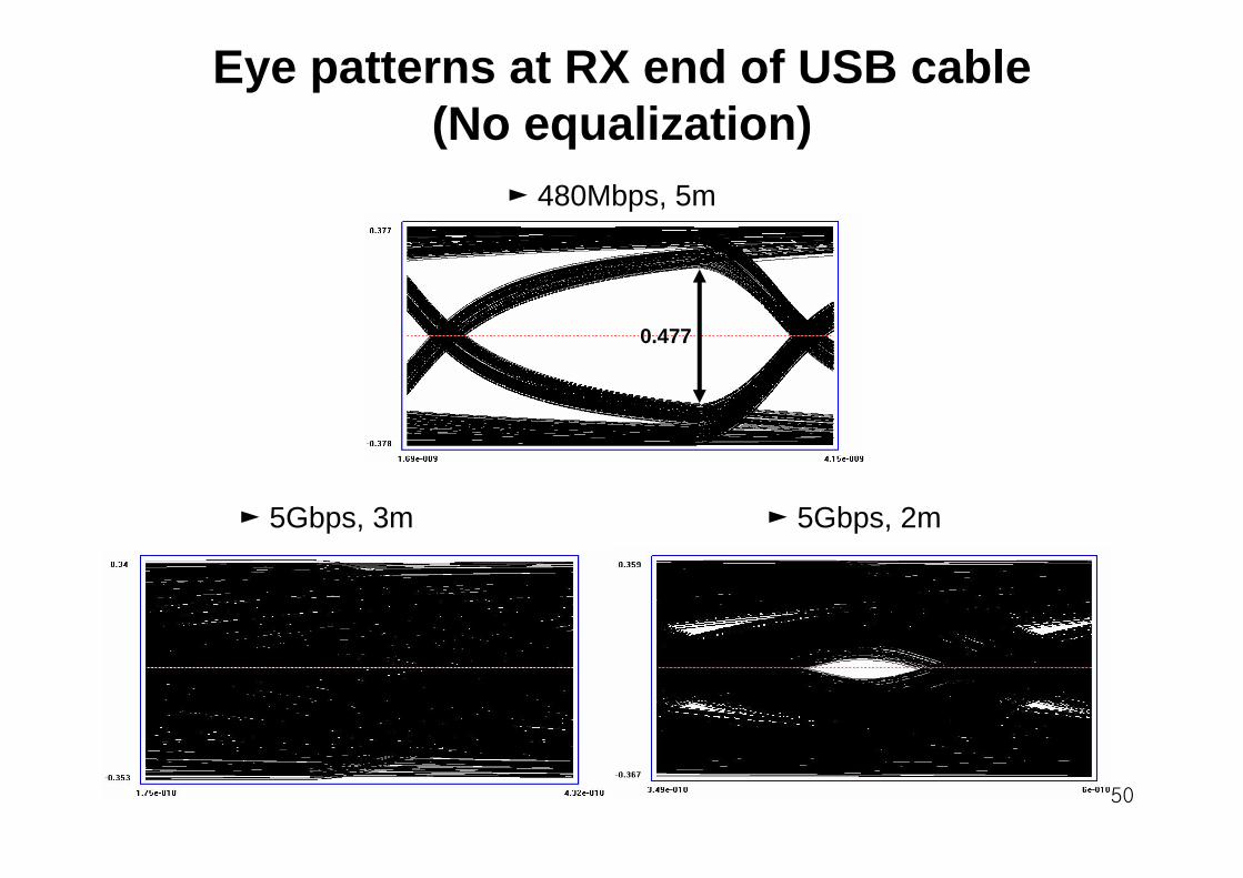
480Mbps, 5m
5Gbps, 3m
0.477
Eye patterns at RX end of USB cable (No equalization)
5Gbps, 2m
51
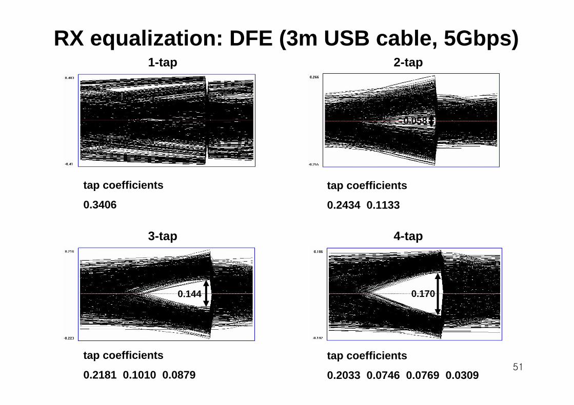
1-tap 2-tap
3-tap 4-tap
0.058
0.144 0.170
tap coefficients
0.3406
tap coefficients
0.2434 0.1133
tap coefficients
0.2181 0.1010 0.0879
tap coefficients
0.2033 0.0746 0.0769 0.0309
RX equalization: DFE (3m USB cable, 5Gbps)
52
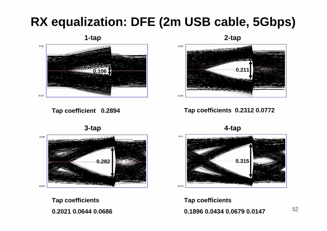
RX equalization: DFE (2m USB cable, 5Gbps)1-tap 2-tap
3-tap 4-tap
Tap coefficient 0.2894
0.106
Tap coefficients 0.2312 0.0772
0.211
Tap coefficients
0.2021 0.0644 0.0686
0.282
Tap coefficients
0.1896 0.0434 0.0679 0.0147
0.315
53
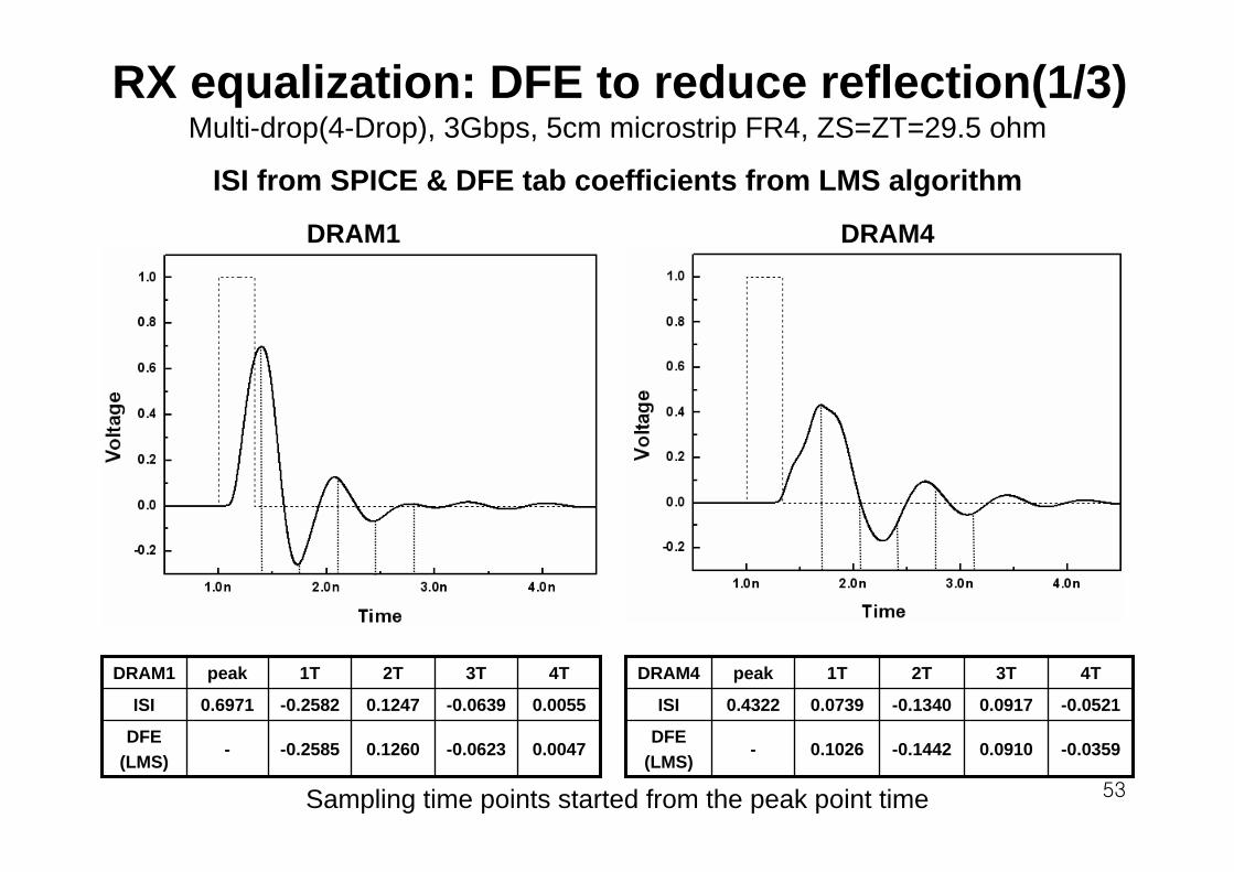
DRAM1
0.0047-0.06230.1260-0.2585-DFE
(LMS)
0.0055-0.06390.1247-0.25820.6971ISI
4T3T2T1TpeakDRAM1
-0.03590.0910-0.14420.1026-DFE
(LMS)
-0.05210.0917-0.13400.07390.4322ISI
4T3T2T1TpeakDRAM4
DRAM4
RX equalization: DFE to reduce reflection(1/3)Multi-drop(4-Drop), 3Gbps, 5cm microstrip FR4, ZS=ZT=29.5 ohm
ISI from SPICE & DFE tab coefficients from LMS algorithm
Sampling time points started from the peak point time
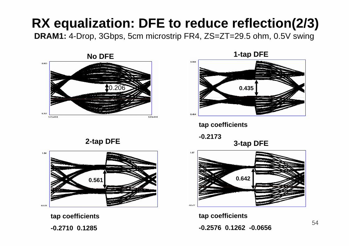
54
3-tap DFE
0.642
tap coefficients
-0.2576 0.1262 -0.0656
1-tap DFE
tap coefficients
-0.2173
0.435
tap coefficients
-0.2710 0.1285
0.561
2-tap DFE
DRAM1: 4-Drop, 3Gbps, 5cm microstrip FR4, ZS=ZT=29.5 ohm, 0.5V swing
0.206
No DFE
RX equalization: DFE to reduce reflection(2/3)
55
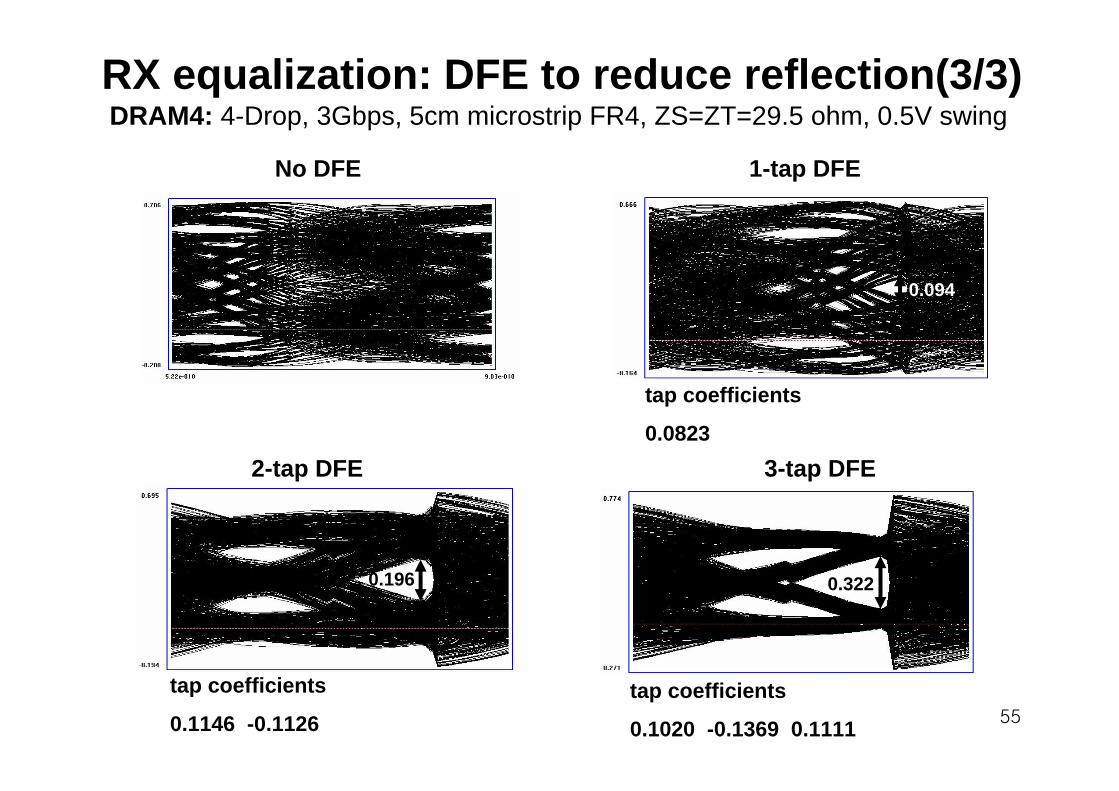
DRAM4: 4-Drop, 3Gbps, 5cm microstrip FR4, ZS=ZT=29.5 ohm, 0.5V swing
No DFE
3-tap DFE
0.322
tap coefficients
0.1020 -0.1369 0.1111
2-tap DFE
0.196
tap coefficients
0.1146 -0.1126
1-tap DFE
tap coefficients
0.0823
0.094
RX equalization: DFE to reduce reflection(3/3)

56
6. Crosstalk & reduction techniques
57
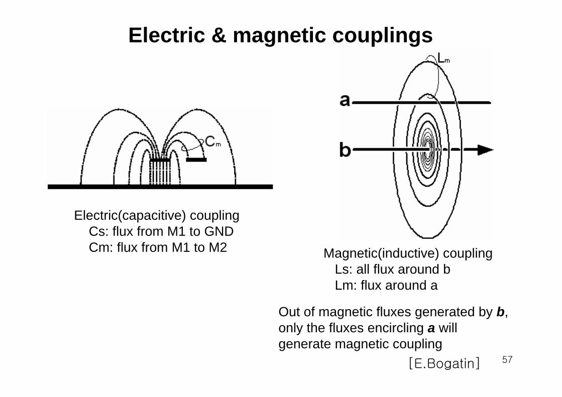
Electric & magnetic couplings
Electric(capacitive) couplingCs: flux from M1 to GND Cm: flux from M1 to M2 Magnetic(inductive) coupling
Ls: all flux around bLm: flux around a
Out of magnetic fluxes generated by b, only the fluxes encircling a will generate magnetic coupling
[E.Bogatin]
58
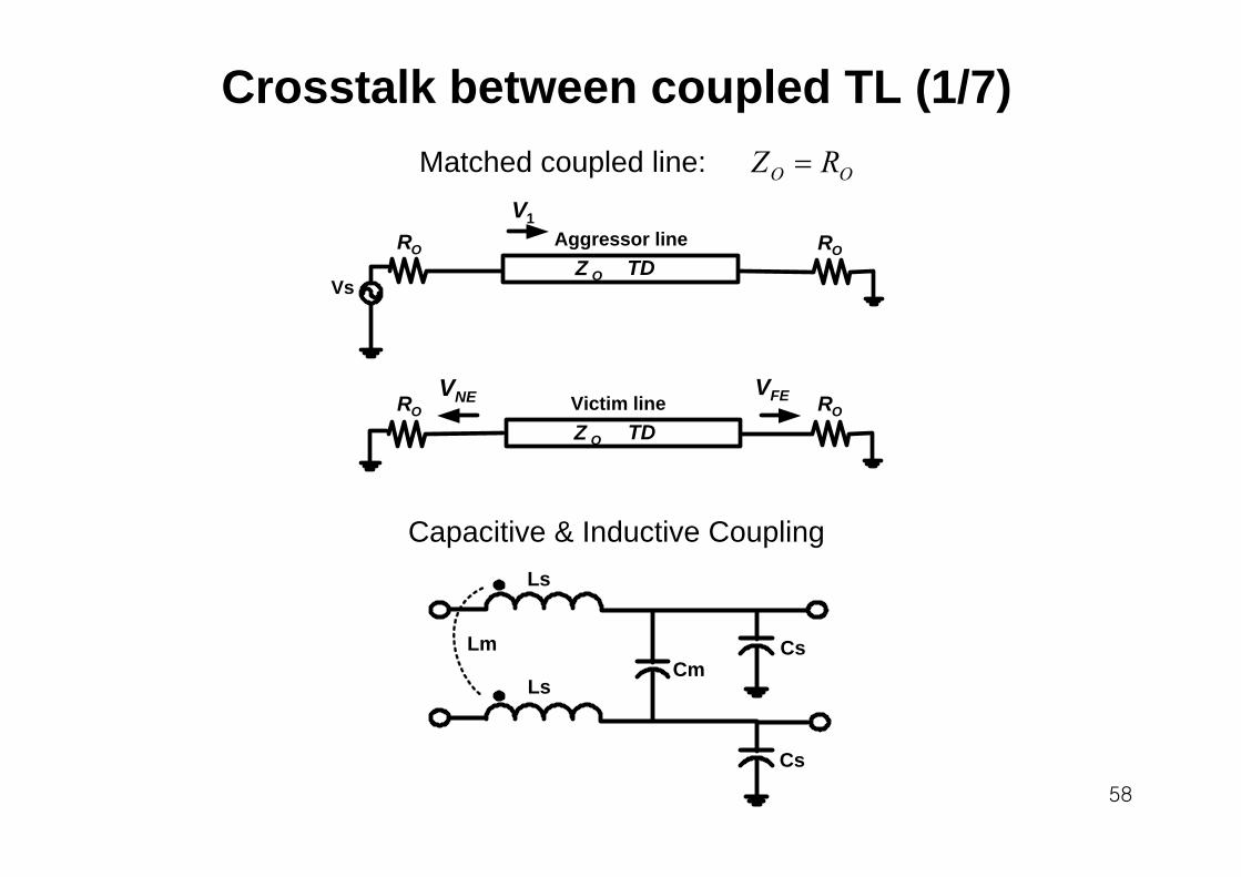
Crosstalk between coupled TL (1/7)
Vs
Aggressor line
Victim line
OZ
1V
FEVNEV
OR
OR
OR
OROZ
TD
TD
Matched coupled line:
Ls
Ls
LmCm
Cs
Cs
Capacitive & Inductive Coupling
OO RZ =
59
Capacitive Coupling
( )dttdVdxCZVd mO
Cτ−
⋅=− 12 2
( )dttdVdxCZVd mO
Cτ−
⋅=+ 12 2
Inductive Coupling
( )dttdVdxLVd m
Lτ−
⋅=− 12 2
( )dttdVdxLVd m
Lτ−
⋅−=+ 12 2
( )( )τ
τ−−
tdtdVdxCm
1
OZ
+CdV2
−CdV2
OZ
Aggressor Line
Victim Line
( )( )τ
τ−−
tdtdIdxLm
1
OZ
−LdV2
+LdV2
OZVictim Line
Crosstalk between coupled TL (2/7)
60
( )dttdV
ZLCZdxdV
O
mmONE
τ22
1 −⎟⎟⎠
⎞⎜⎜⎝
⎛+=
( )dt
TDtdVZLCZdxdV
O
mmOFE
−⎟⎟⎠
⎞⎜⎜⎝
⎛−= 1
2
Capacitive + Inductive
After integration with x along length l
( ) ( ) ( )( )TDtVtVLL
CCtV
S
m
T
mNE 2
41
11 −−⎟⎟⎠
⎞⎜⎜⎝
⎛+=
( ) ( )t
TDtVLL
CCTDtV
S
m
T
mFE ∂
−∂⎟⎟⎠
⎞⎜⎜⎝
⎛−= 1
2
Near-end crosstalk (NEXT):
Far-end crosstalk (FEXT):
Crosstalk between coupled TL (3/7)
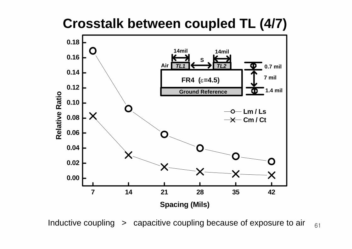
61Inductive coupling > capacitive coupling because of exposure to air
7 14 21 28 35 42
0.00
0.02
0.04
0.06
0.08
0.10
0.12
0.14
0.16
0.18
Rel
ativ
e R
atio
Spacing (Mils)
Lm / Ls Cm / Ct
0.7 mil
7 mil
1.4 mil
Air
FR4 (ε=4.5)
14milS
14mil
Ground Reference
TL1 TL2
Crosstalk between coupled TL (4/7)
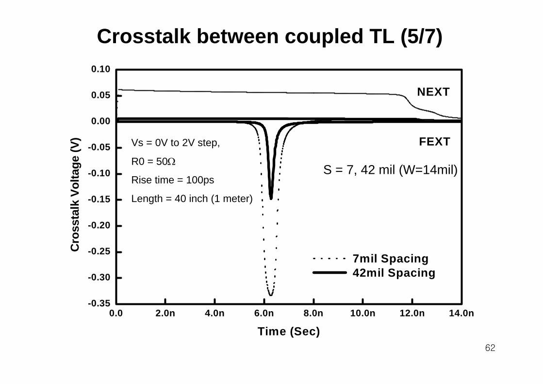
62
S = 7, 42 mil (W=14mil)
0.0 2.0n 4.0n 6.0n 8.0n 10.0n 12.0n 14.0n-0.35
-0.30
-0.25
-0.20
-0.15
-0.10
-0.05
0.00
0.05
0.10
FEXT
NEXTC
ross
talk
Vol
tage
(V)
Time (Sec)
7mil Spacing 42mil Spacing
Vs = 0V to 2V step,
R0 = 50Ω
Rise time = 100ps
Length = 40 inch (1 meter)
Crosstalk between coupled TL (5/7)
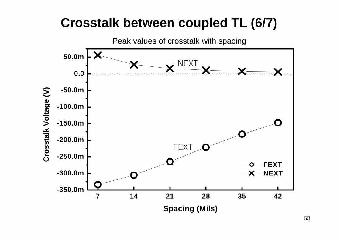
63
Peak values of crosstalk with spacing
7 14 21 28 35 42-350.0m
-300.0m
-250.0m
-200.0m
-150.0m
-100.0m
-50.0m
0.0
50.0mC
ross
talk
Vol
tage
(V)
Spacing (Mils)
FEXT NEXT
NEXT
FEXT
Crosstalk between coupled TL (6/7)
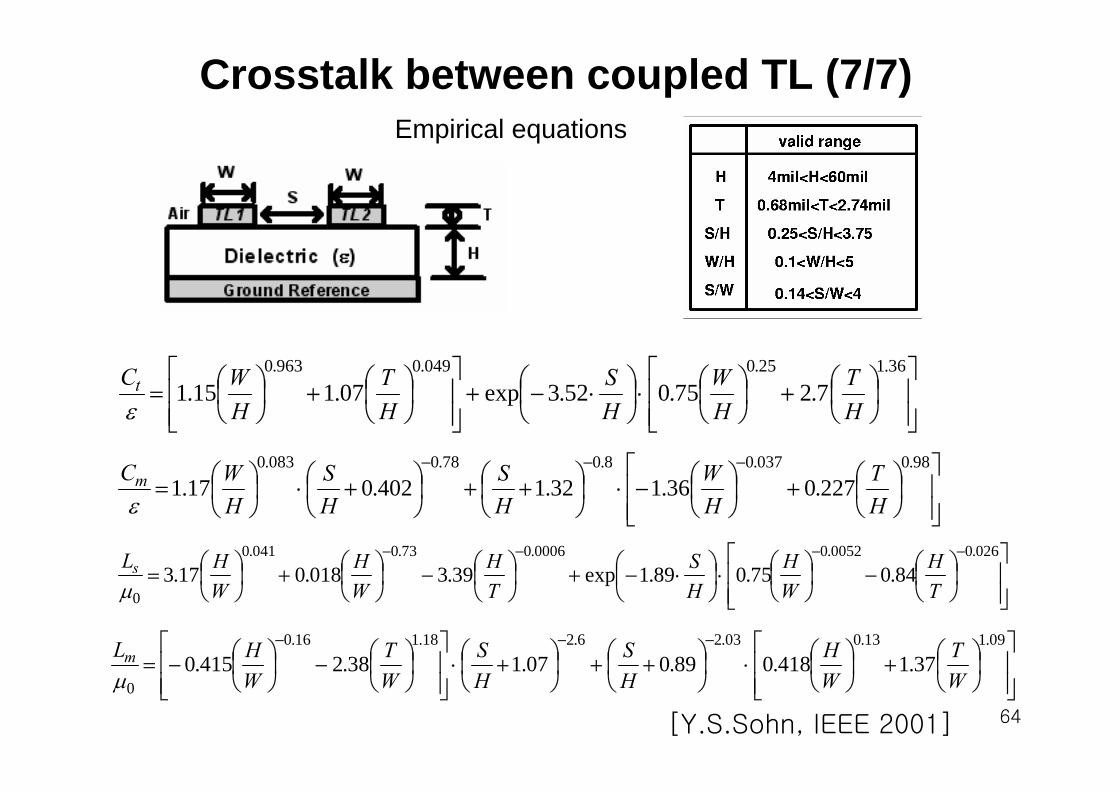
64
Empirical equations
Crosstalk between coupled TL (7/7)
[Y.S.Sohn, IEEE 2001]
⎥⎥⎦
⎤
⎢⎢⎣
⎡⎟⎠⎞
⎜⎝⎛+⎟
⎠⎞
⎜⎝⎛⋅⎟
⎠⎞
⎜⎝⎛ ⋅−+
⎥⎥⎦
⎤
⎢⎢⎣
⎡⎟⎠⎞
⎜⎝⎛+⎟
⎠⎞
⎜⎝⎛=
36.125.0049.0963.0
7.275.052.3exp07.115.1HT
HW
HS
HT
HWCt
ε
⎥⎥⎦
⎤
⎢⎢⎣
⎡⎟⎠⎞
⎜⎝⎛+⎟
⎠⎞
⎜⎝⎛−⋅⎟
⎠⎞
⎜⎝⎛ ++⎟
⎠⎞
⎜⎝⎛ +⋅⎟
⎠⎞
⎜⎝⎛=
−−− 98.0037.08.078.0083.0
227.036.132.1402.017.1HT
HW
HS
HS
HWCm
ε
⎥⎥⎦
⎤
⎢⎢⎣
⎡⎟⎠⎞
⎜⎝⎛−⎟
⎠⎞
⎜⎝⎛⋅⎟
⎠⎞
⎜⎝⎛ ⋅−+⎟
⎠⎞
⎜⎝⎛−⎟
⎠⎞
⎜⎝⎛+⎟
⎠⎞
⎜⎝⎛=
−−−− 026.00052.00006.073.0041.0
084.075.089.1exp39.3018.017.3
TH
WH
HS
TH
WH
WHLs
µ
⎥⎥⎦
⎤
⎢⎢⎣
⎡⎟⎠⎞
⎜⎝⎛+⎟
⎠⎞
⎜⎝⎛⋅⎟
⎠⎞
⎜⎝⎛ ++⎟
⎠⎞
⎜⎝⎛ +⋅
⎥⎥⎦
⎤
⎢⎢⎣
⎡⎟⎠⎞
⎜⎝⎛−⎟
⎠⎞
⎜⎝⎛−=
−−− 09.113.003.26.218.116.0
037.1418.089.007.138.2415.0
WT
WH
HS
HS
WT
WHLm
µ
65
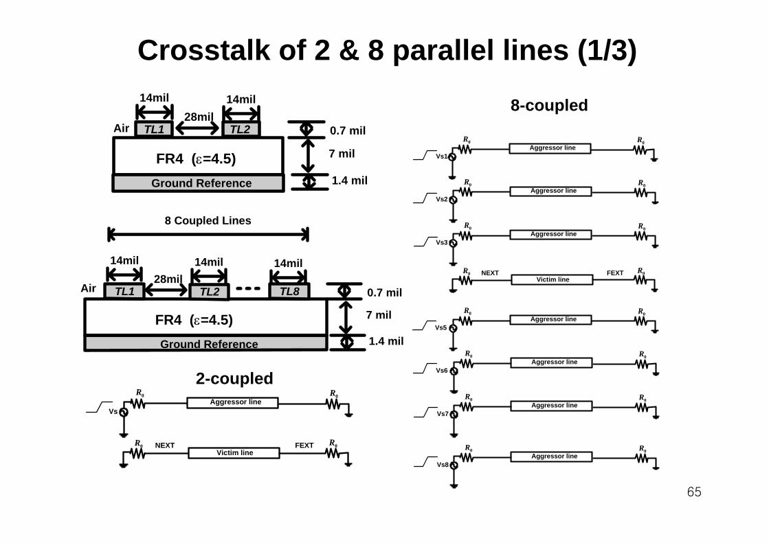
Crosstalk of 2 & 8 parallel lines (1/3)
Aggressor line0R 0R
0R 0R
Vs
Victim lineNEXT FEXT
2-coupled
Aggressor line0R 0R
0R 0R
Vs3
Victim lineNEXT FEXT
Aggressor line0R 0R
Vs2
Aggressor line0R 0R
Vs1
Aggressor line0R 0R
Vs7
Aggressor line0R 0R
Vs6
Aggressor line0R 0R
Vs5
Aggressor line0R 0R
Vs8
8-coupled0.7 mil
7 mil
1.4 mil
Air
FR4 (ε=4.5)
14mil28mil
14mil
Ground Reference
TL1 TL2
0.7 mil
7 mil
1.4 mil
Air
FR4 (ε=4.5)
14mil28mil
14mil 14mil
8 Coupled Lines
TL1
Ground Reference
TL2 TL8
66
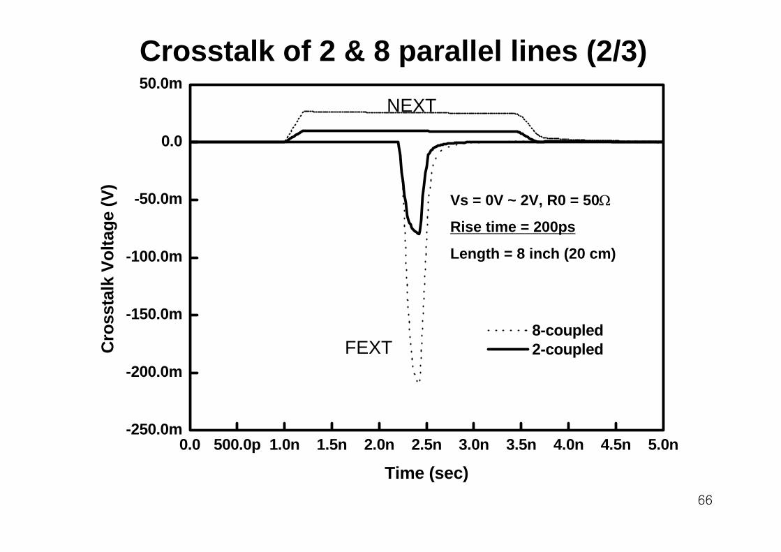
Crosstalk of 2 & 8 parallel lines (2/3)NEXT
FEXT
Vs = 0V ~ 2V, R0 = 50Ω
Rise time = 200ps
Length = 8 inch (20 cm)
0.0 500.0p 1.0n 1.5n 2.0n 2.5n 3.0n 3.5n 4.0n 4.5n 5.0n-250.0m
-200.0m
-150.0m
-100.0m
-50.0m
0.0
50.0mC
ross
talk
Vol
tage
(V)
Time (sec)
8-coupled 2-coupled
67
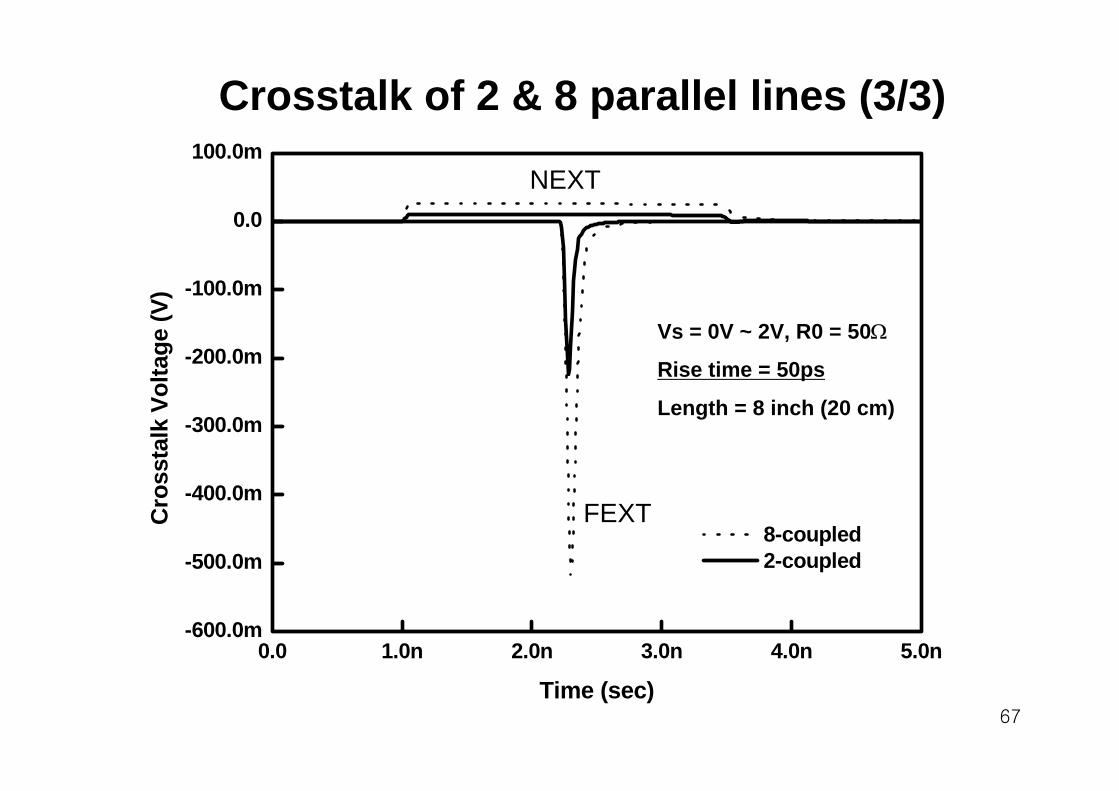
0.0 1.0n 2.0n 3.0n 4.0n 5.0n-600.0m
-500.0m
-400.0m
-300.0m
-200.0m
-100.0m
0.0
100.0mC
ross
talk
Vol
tage
(V)
Time (sec)
8-coupled 2-coupled
Crosstalk of 2 & 8 parallel lines (3/3)
NEXT
Vs = 0V ~ 2V, R0 = 50Ω
Rise time = 50ps
Length = 8 inch (20 cm)
FEXT
68
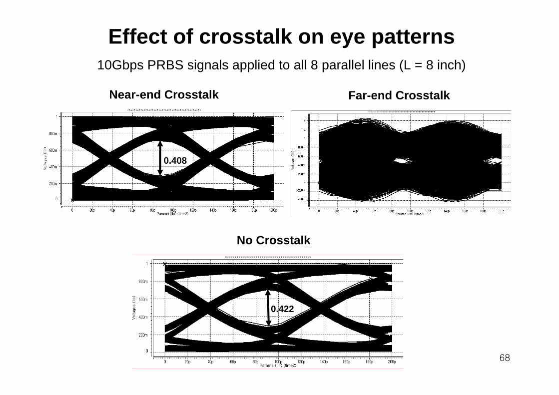
Far-end CrosstalkNear-end Crosstalk
No Crosstalk
0.408
0.422
Effect of crosstalk on eye patterns10Gbps PRBS signals applied to all 8 parallel lines (L = 8 inch)
69
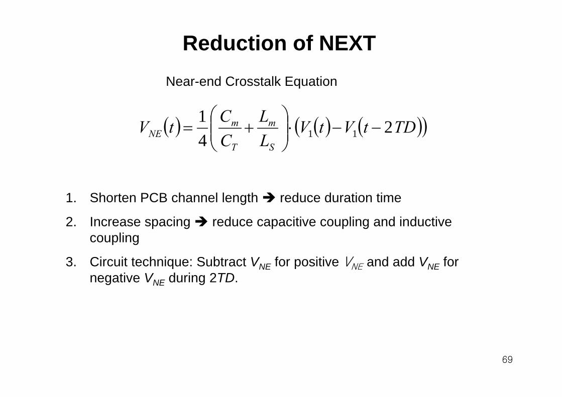
Reduction of NEXT
1. Shorten PCB channel length reduce duration time
2. Increase spacing reduce capacitive coupling and inductive coupling
3. Circuit technique: Subtract VNE for positive VNE and add VNE for negative VNE during 2TD.
Near-end Crosstalk Equation
( ) ( ) ( )( )TDtVtVLL
CCtV
S
m
T
mNE 2
41
11 −−⋅⎟⎟⎠
⎞⎜⎜⎝
⎛+=
70
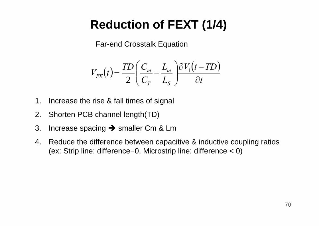
Reduction of FEXT (1/4)
1. Increase the rise & fall times of signal
2. Shorten PCB channel length(TD)
3. Increase spacing smaller Cm & Lm
4. Reduce the difference between capacitive & inductive coupling ratios (ex: Strip line: difference=0, Microstrip line: difference < 0)
Far-end Crosstalk Equation
( ) ( )t
TDtVLL
CCTDtV
S
m
T
mFE ∂
−∂⎟⎟⎠
⎞⎜⎜⎝
⎛−= 1
2
71
5. Add a capacitor at receiver side between aggressor and victim lines
Inductive coupling > capacitive coupling, in FR4 microstrip line because of exposure to air
Adding capacitor at RX reduces the difference between two couplings
V s
A g g r e s s o r l in e
V ic t im l in e
OR
OR OR
OR1V
F EV
OZ T D
OZ T DAdded Capacitor
PC
[Guggenbuhl 1993]
0.082840.1692
( )mHLS ( )mFCTS
mL
LT
mC
C
n8.296 p1.131
1692.0==+⋅+⋅
S
m
PT
Pm
LL
ClCClC pFCP 63.13=∴
Reduction of FEXT (2/4)Unidirectional channel
72
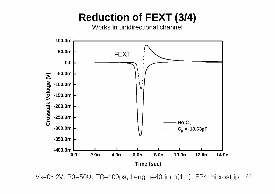
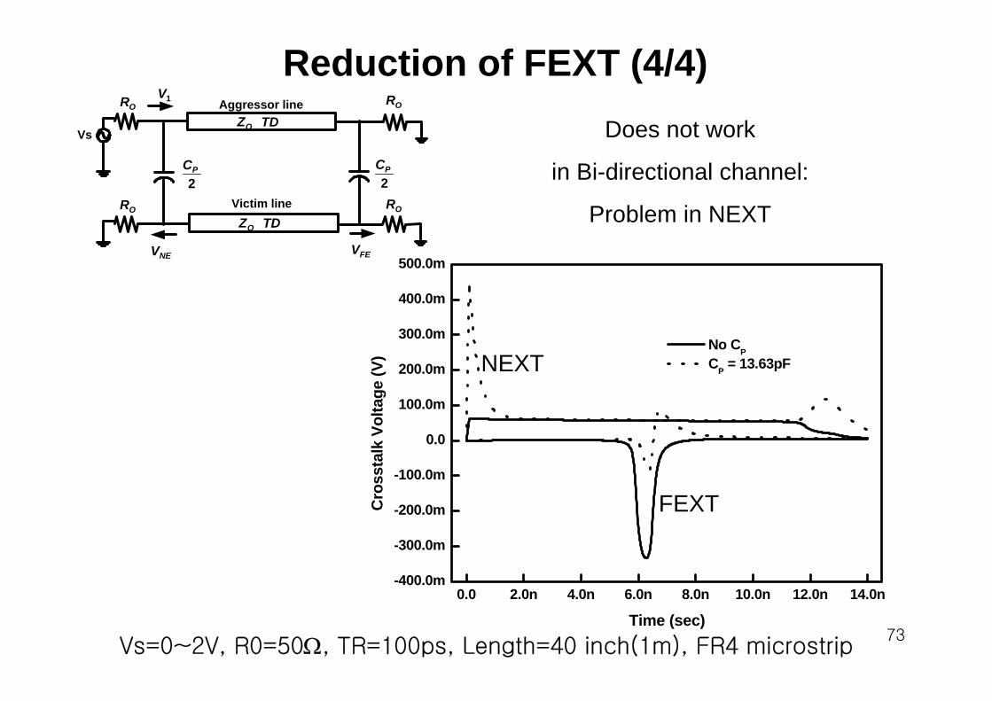
Reduction of FEXT (3/4)Works in unidirectional channel
Vs=0~2V, R0=50Ω, TR=100ps, Length=40 inch(1m), FR4 microstrip
0.0 2.0n 4.0n 6.0n 8.0n 10.0n 12.0n 14.0n-400.0m
-350.0m
-300.0m
-250.0m
-200.0m
-150.0m
-100.0m
-50.0m
0.0
50.0m
100.0mC
ross
talk
Vol
tage
(V)
Time (sec)
No CP CP = 13.63pF
FEXT
73
Reduction of FEXT (4/4)Vs
Aggressor line
Victim line
OR
OR OR
OR1V
FEV
OZ TD
OZ TD
2PC
2PC
NEV
0.0 2.0n 4.0n 6.0n 8.0n 10.0n 12.0n 14.0n-400.0m
-300.0m
-200.0m
-100.0m
0.0
100.0m
200.0m
300.0m
400.0m
500.0m
Cro
ssta
lk V
olta
ge (V
)
Time (sec)
No CP CP = 13.63pFNEXT
FEXT
Does not work
in Bi-directional channel:
Problem in NEXT
Vs=0~2V, R0=50Ω, TR=100ps, Length=40 inch(1m), FR4 microstrip
74
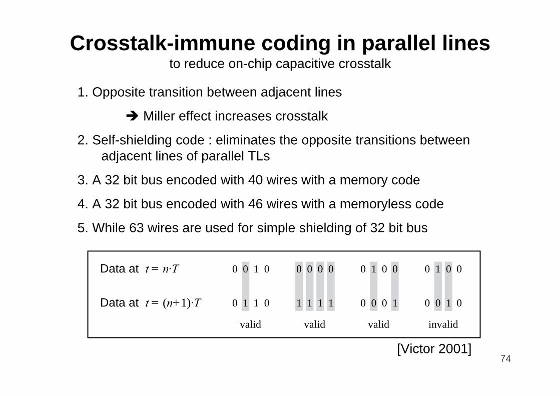
Crosstalk-immune coding in parallel lines to reduce on-chip capacitive crosstalk
[Victor 2001]
1. Opposite transition between adjacent lines
Miller effect increases crosstalk
2. Self-shielding code : eliminates the opposite transitions between adjacent lines of parallel TLs
3. A 32 bit bus encoded with 40 wires with a memory code
4. A 32 bit bus encoded with 46 wires with a memoryless code
5. While 63 wires are used for simple shielding of 32 bit bus
Data at t = n·T
Data at t = (n+1)·T
valid
0 0 1 0 0 0 0 0 0 1 0 0 0 1 0 0
0 1 1 0 1 1 1 1 0 0 0 1 0 0 1 0
valid valid invalid
75
7. IBIS (I/O Buffer Information Spec) model
and power integrity
76
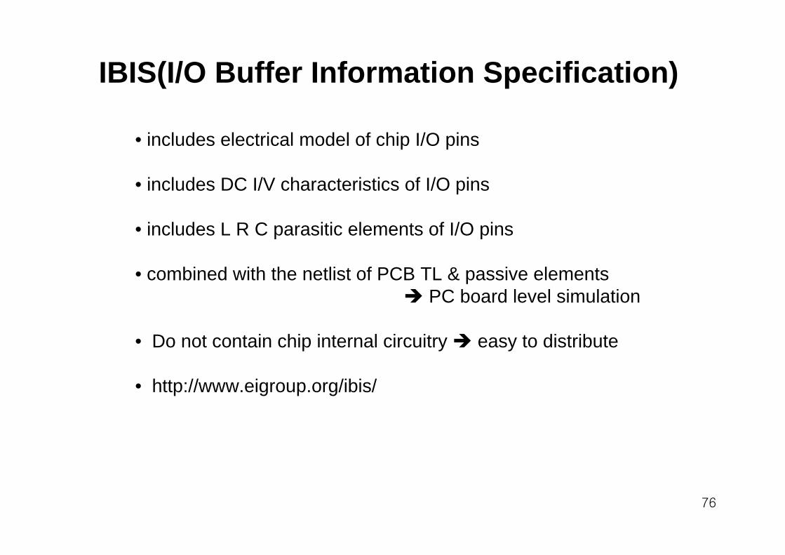
IBIS(I/O Buffer Information Specification)
• includes electrical model of chip I/O pins
• includes DC I/V characteristics of I/O pins
• includes L R C parasitic elements of I/O pins
• combined with the netlist of PCB TL & passive elements PC board level simulation
• Do not contain chip internal circuitry easy to distribute
• http://www.eigroup.org/ibis/
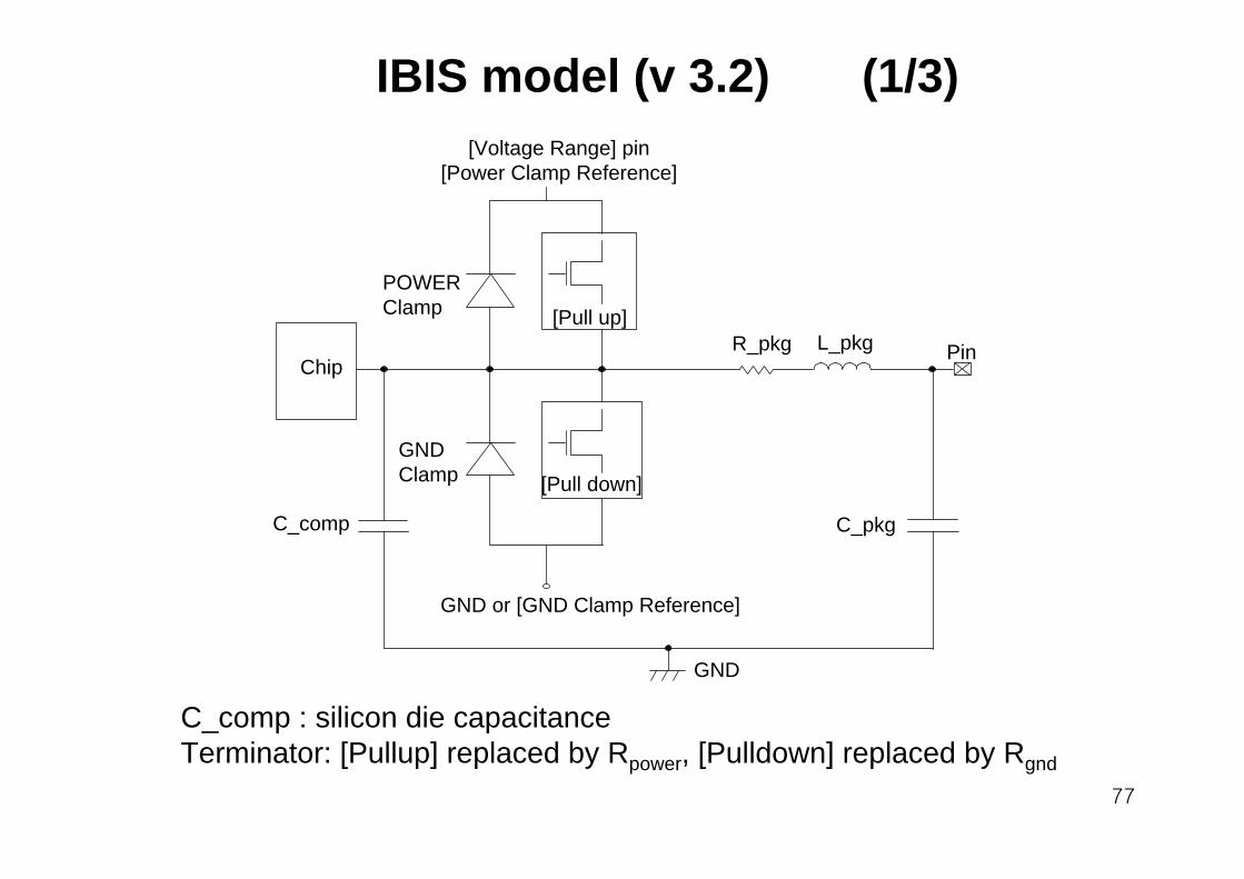
77
IBIS model (v 3.2) (1/3)[Voltage Range] pin
[Power Clamp Reference]
Chip
GND
Pin
GND or [GND Clamp Reference]
GND Clamp [Pull down]
[Pull up]
C_comp C_pkg
R_pkg L_pkg
POWER Clamp
C_comp : silicon die capacitanceTerminator: [Pullup] replaced by Rpower, [Pulldown] replaced by Rgnd
78
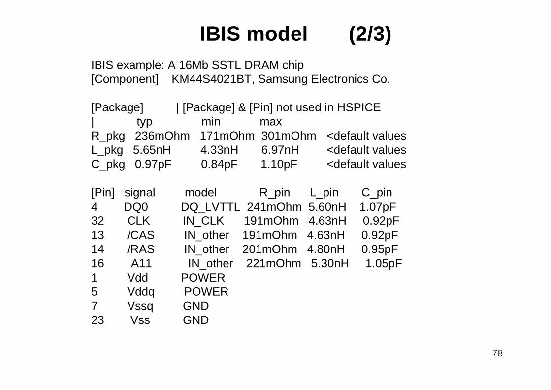
IBIS example: A 16Mb SSTL DRAM chip[Component] KM44S4021BT, Samsung Electronics Co.
[Package] | [Package] & [Pin] not used in HSPICE| typ min maxR_pkg 236mOhm 171mOhm 301mOhm <default values L_pkg 5.65nH 4.33nH 6.97nH <default values C_pkg 0.97pF 0.84pF 1.10pF <default values
[Pin] signal model R_pin L_pin C_pin4 DQ0 DQ_LVTTL 241mOhm 5.60nH 1.07pF32 CLK IN_CLK 191mOhm 4.63nH 0.92pF13 /CAS IN_other 191mOhm 4.63nH 0.92pF14 /RAS IN_other 201mOhm 4.80nH 0.95pF16 A11 IN_other 221mOhm 5.30nH 1.05pF1 Vdd POWER5 Vddq POWER7 Vssq GND23 Vss GND
IBIS model (2/3)
79
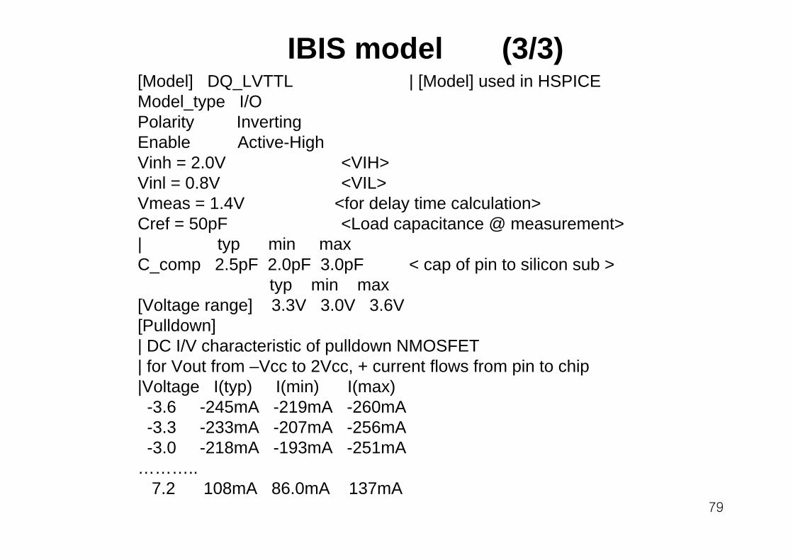
[Model] DQ_LVTTL | [Model] used in HSPICEModel_type I/OPolarity InvertingEnable Active-HighVinh = 2.0V <VIH>Vinl = 0.8V <VIL>Vmeas = 1.4V <for delay time calculation>Cref = 50pF <Load capacitance @ measurement>| typ min maxC_comp 2.5pF 2.0pF 3.0pF < cap of pin to silicon sub >
typ min max[Voltage range] 3.3V 3.0V 3.6V[Pulldown]| DC I/V characteristic of pulldown NMOSFET | for Vout from –Vcc to 2Vcc, + current flows from pin to chip|Voltage I(typ) I(min) I(max)-3.6 -245mA -219mA -260mA-3.3 -233mA -207mA -256mA-3.0 -218mA -193mA -251mA
………..7.2 108mA 86.0mA 137mA
IBIS model (3/3)
80
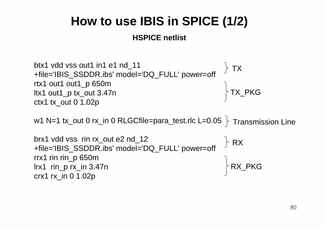
btx1 vdd vss out1 in1 e1 nd_11 +file='IBIS_SSDDR.ibs' model='DQ_FULL' power=offrtx1 out1 out1_p 650mltx1 out1_p tx_out 3.47nctx1 tx_out 0 1.02p
w1 N=1 tx_out 0 rx_in 0 RLGCfile=para_test.rlc L=0.05
brx1 vdd vss rin rx_out e2 nd_12 +file='IBIS_SSDDR.ibs' model='DQ_FULL' power=offrrx1 rin rin_p 650mlrx1 rin_p rx_in 3.47ncrx1 rx_in 0 1.02p
TX
TX_PKG
RX
RX_PKG
Transmission Line
How to use IBIS in SPICE (1/2) HSPICE netlist
81
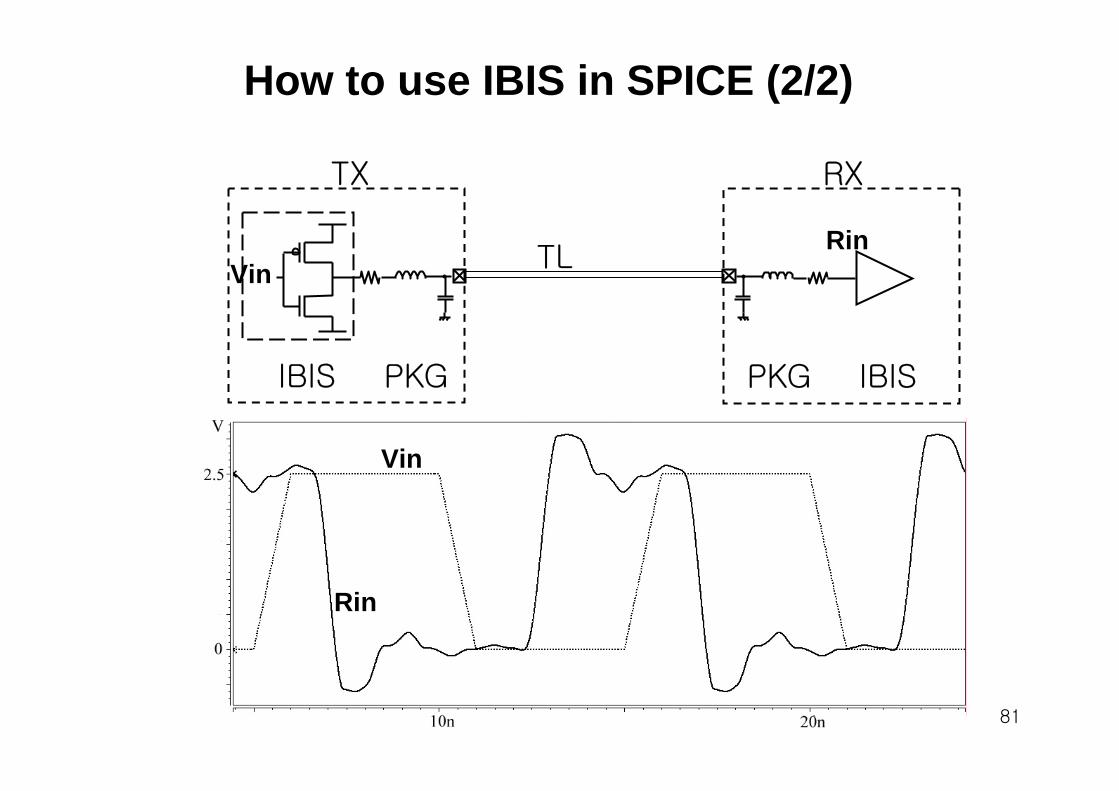
How to use IBIS in SPICE (2/2)
TL
IBIS PKG
TX
Vin
IBISPKG
RX
Rin
Vin
Rin
82
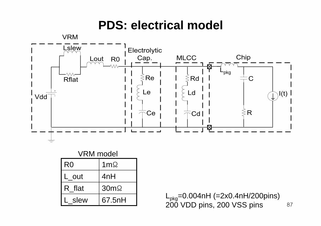
Power Integrity PDS: power distribution system
To reduce ground bounce & supply droop,keep a small VDD-VSS impedance at all frequencies
At low frequency use decoupling capacitor to reduce VDD-VSS impedance
At high frequency minimize loop inductance of decoupling cap & chip’s pad
How to design PDS(1) Use a voltage regulator module(VRM) to keep low impedance
at very low frequency up to several kHz(2) Determine the value of electrolytic cap for low frequency(3) Determine the target impedance seen by chip(4) Decide ceramic capacitors with different resonant frequencies
to keep the impedance low at high frequency(5) Decide the on-chip bypass capacitor(OBC) value to keep low
impedance for frequencies of several hundred or MHz higher
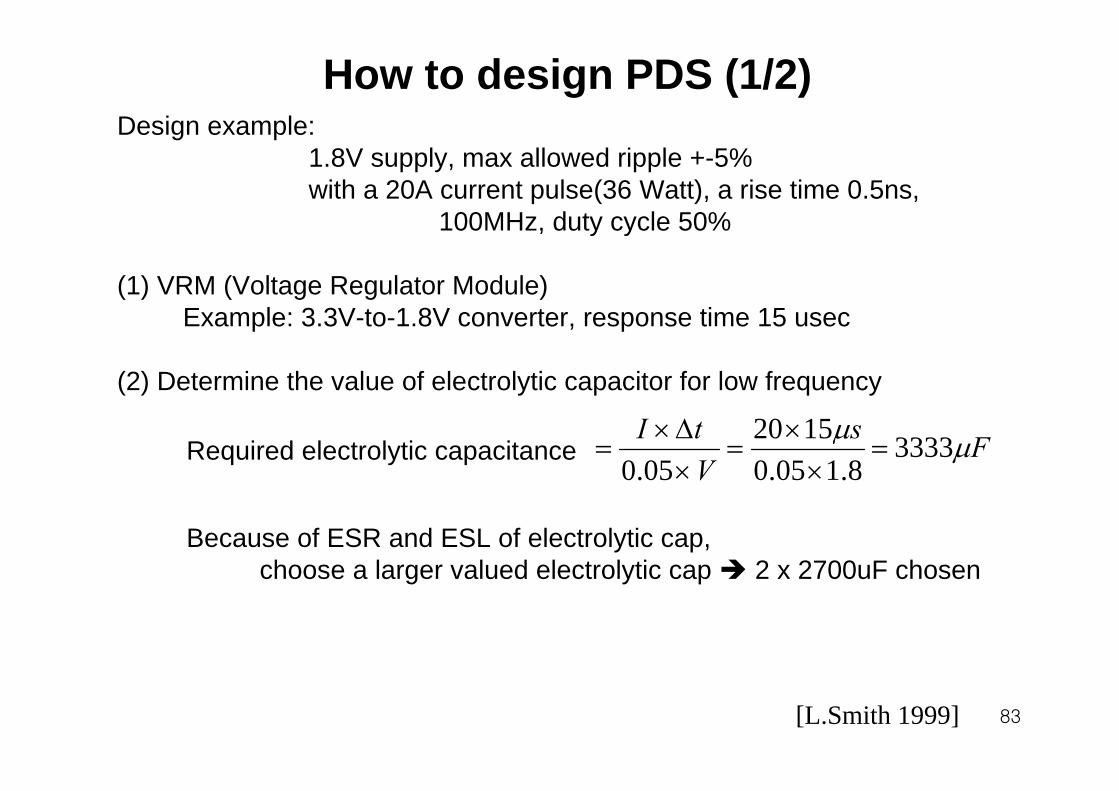
83
Design example: 1.8V supply, max allowed ripple +-5% with a 20A current pulse(36 Watt), a rise time 0.5ns,
100MHz, duty cycle 50%
(1) VRM (Voltage Regulator Module)Example: 3.3V-to-1.8V converter, response time 15 usec
(2) Determine the value of electrolytic capacitor for low frequency
How to design PDS (1/2)
Because of ESR and ESL of electrolytic cap, choose a larger valued electrolytic cap 2 x 2700uF chosen
FsVtI µµ 3333
8.105.01520
05.0=
××
=×∆×
=Required electrolytic capacitance
[L.Smith 1999]
84
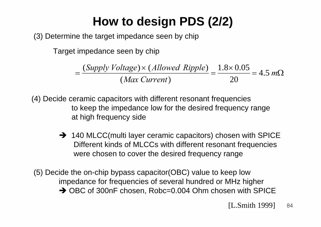
(3) Determine the target impedance seen by chip
How to design PDS (2/2)
Ω=×
=×
= mCurrentMax
RippleAllowedVoltageSupply 5.420
05.08.1)(
)()(
Target impedance seen by chip
[L.Smith 1999]
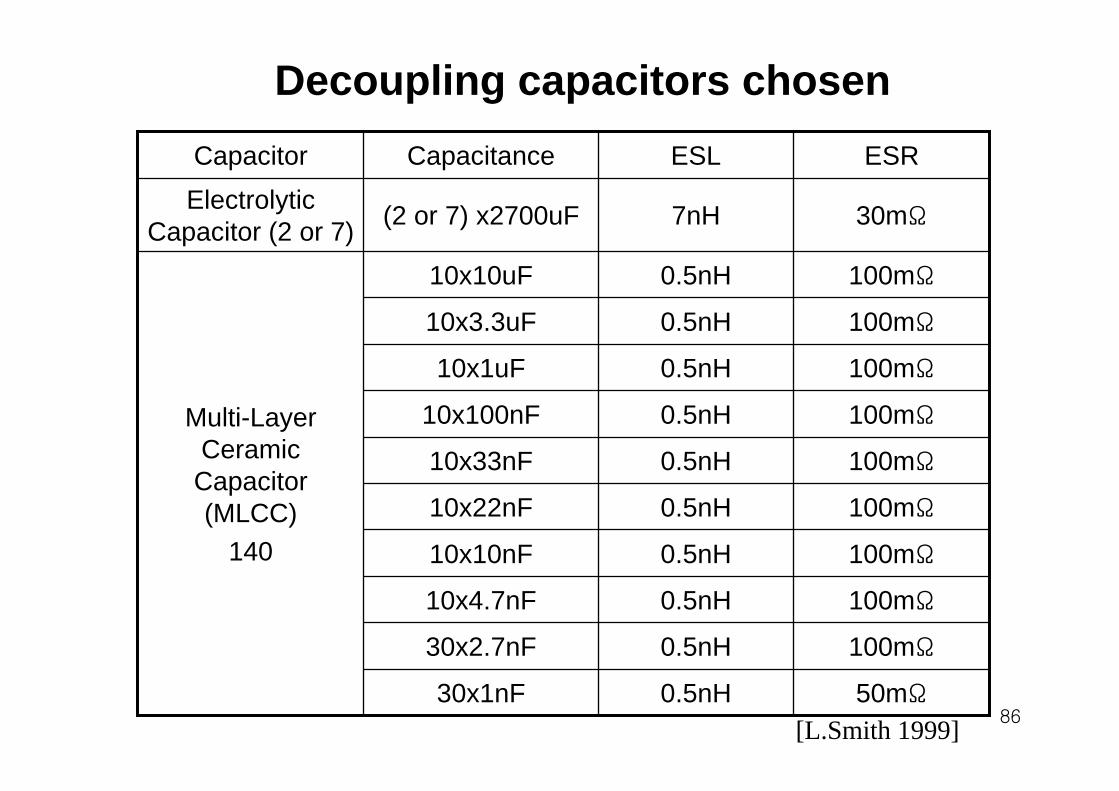
(4) Decide ceramic capacitors with different resonant frequencies to keep the impedance low for the desired frequency range at high frequency side
140 MLCC(multi layer ceramic capacitors) chosen with SPICEDifferent kinds of MLCCs with different resonant frequencies were chosen to cover the desired frequency range
(5) Decide the on-chip bypass capacitor(OBC) value to keep low impedance for frequencies of several hundred or MHz higher
OBC of 300nF chosen, Robc=0.004 Ohm chosen with SPICE
85
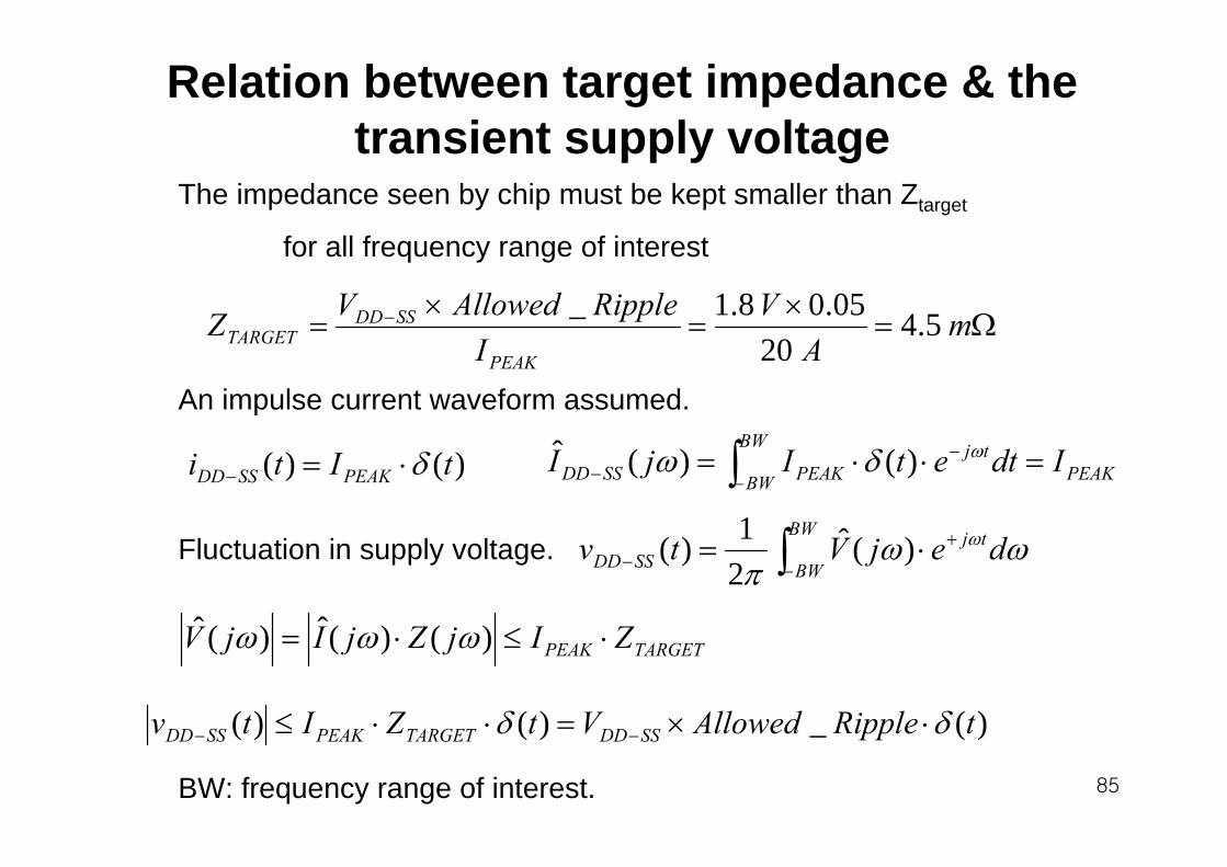
Relation between target impedance & the transient supply voltage
The impedance seen by chip must be kept smaller than Ztarget
for all frequency range of interest
Ω=×
=×
= − mA
VI
RippleAllowedVZPEAK
SSDDTARGET 5.4
2005.08.1_
An impulse current waveform assumed.
)()( tIti PEAKSSDD δ⋅=−
∫−+
− ⋅=BW
BW
tjSSDD dejVtv ωω
πω)(ˆ
21)(
PEAK
BW
BW
tjPEAKSSDD IdtetIjI =⋅⋅= ∫−
−−
ωδω )()(ˆ
TARGETPEAK ZIjZjIjV ⋅≤⋅= )()(ˆ)(ˆ ωωω
)(_)()( tRippleAllowedVtZItv SSDDTARGETPEAKSSDD δδ ⋅×=⋅⋅≤ −−
Fluctuation in supply voltage.
BW: frequency range of interest.
86
Decoupling capacitors chosen
50mΩ0.5nH30x1nF
100mΩ0.5nH30x2.7nF
100mΩ0.5nH10x4.7nF
100mΩ0.5nH10x10nF
100mΩ0.5nH10x22nF
100mΩ0.5nH10x33nF
100mΩ0.5nH10x100nF
100mΩ0.5nH10x1uF
Multi-Layer Ceramic
Capacitor (MLCC)
140
Electrolytic Capacitor (2 or 7)
Capacitor
100mΩ0.5nH10x3.3uF
100mΩ0.5nH10x10uF
30mΩ7nH(2 or 7) x2700uF
ESRESLCapacitance
[L.Smith 1999]
87
PDS: electrical model
1mΩR0
67.5nHL_slew30mΩR_flat4nHL_out
Lpkg
VRM model
Lpkg=0.004nH (=2x0.4nH/200pins)200 VDD pins, 200 VSS pins
88
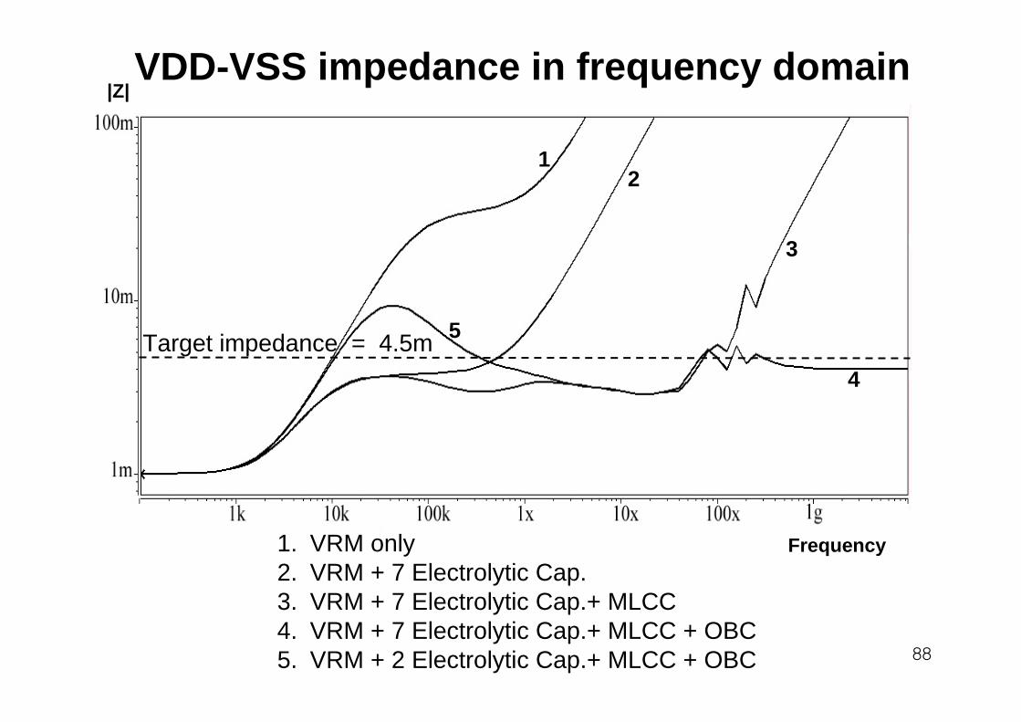
VDD-VSS impedance in frequency domain
1. VRM only2. VRM + 7 Electrolytic Cap.3. VRM + 7 Electrolytic Cap.+ MLCC4. VRM + 7 Electrolytic Cap.+ MLCC + OBC5. VRM + 2 Electrolytic Cap.+ MLCC + OBC
Target impedance = 4.5m
12
3
Frequency
4
5
|Z|
89
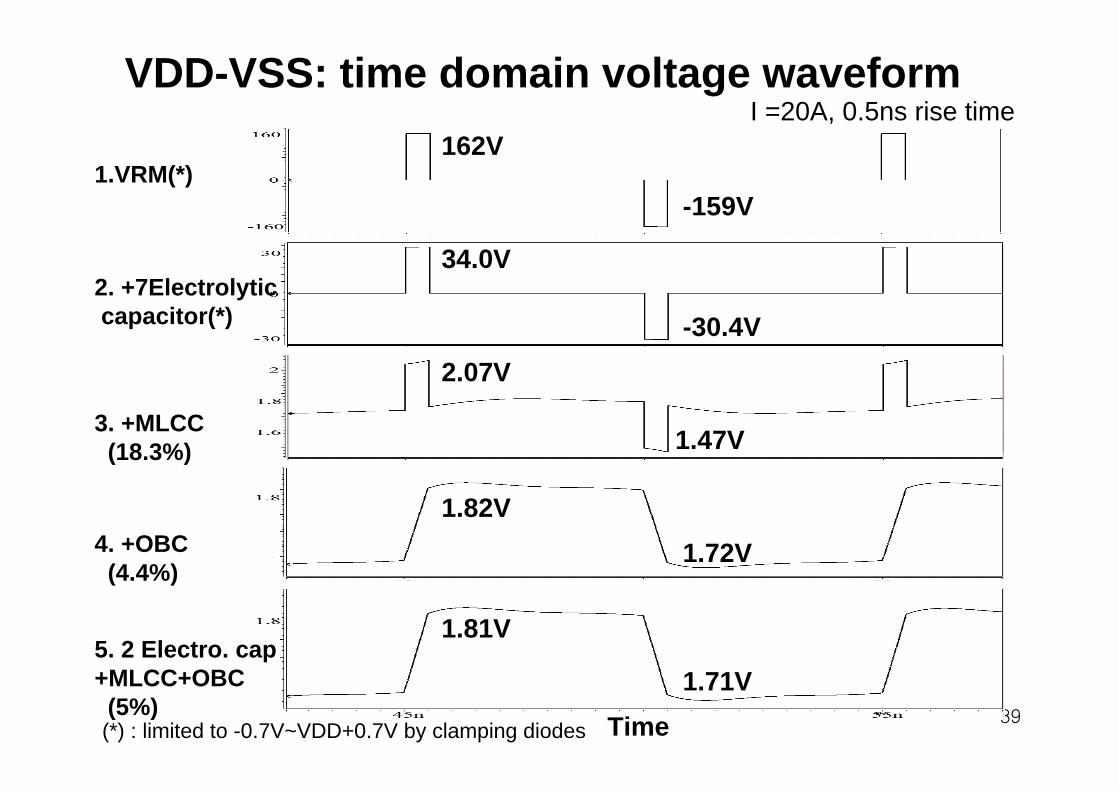
VDD-VSS: time domain voltage waveform
(*) : limited to -0.7V~VDD+0.7V by clamping diodes
I =20A, 0.5ns rise time
Time
162V
-159V
34.0V
-30.4V2.07V
1.47V
1.82V1.72V
1.VRM(*)
2. +7Electrolyticcapacitor(*)
3. +MLCC(18.3%)
4. +OBC(4.4%)
5. 2 Electro. cap +MLCC+OBC(5%)
1.81V
1.71V
90
8. References1. E. Bogatin, “Signal Integrity Simplified”, Prentice Hall, 20042. B.Gunning, L.Yuan, T.Nguyen, T.Wong, “A CMOS Low-Voltage-Swing Transmission-Line
Transceiver”, ISSCC 1992 Digest, pp.58-593. H.W.Johnson, “High-Speed Digital Design: A Handbook of Black Magic”, Prentice Hall, 1993 4. S.H.Hall, G.W.Hall, J.A.McCall, “High-Speed Digital System Design: A Handbook of
Interconnect Theory and Design Practices”, John Wiley & Sons, 20005. H.Johnson, M.Graham, “High-Speed Signal Propagation: Advanced Black Magic”, Prentice Hall,
20036. H.W.Ott, “Noise Reduction Techniques in Electronic Systems”, 2nd Edition, John Wiley & Sons,
19887. H.B.Lee, K. Lee, H.K.Jung, H.J.Park, "Extraction of LRGC Matrices for 8-coupled uniform lossy
transmission lines using 2-port VNA Measurements", IEICE Trans. on Electronics, vol.E89-C, no.3, Mar. 2006.
8. Y.S.Sohn, J.C.Lee, H.J.Park, S.I.Cho, “Empirical Equations on Electrical Parameters of Coupled Microstrip Lines for Crosstalk Estimation in Printed Circuit Board”, IEEE Trans. Advanced Packaging, vol.24, no.4, Nov.2001, pp.521-527
9. W.Guggenbuhl, G.Morbach, “Forward Crosstalk Compensation on Bus Lines”, IEEE Trans. Circuits and Systems-I: Fundamental Theory and Applications, Vol.40, No.8, Aug, pp.523–527, 1993
10. B.Victor, K.Keutzer, “Bus Encoding to Prevent Crosstalk Delay”, IEEE/ACM International Conference on Computer Aided Design, Nov, pp. 57 – 63, 2001
11. L.D.Smith, R.E.Anderson, D.W.Forehand, T.J.Pelc, T.Roy, “Power Distribution System Design Methodology and Capacitor Selection for Modern CMOS Technology”, IEEE Trans. Advanced Packaging, vol.22, no.3, Aug. 1999, pp.284-291

91
Acknowledgements
Thanks to
Dr. Hyun-Bae Lee,
Mr. Jae-Seung Lee,
Mr. Hyung-Joon Chi,
Mr. Kyoung-Ho Lee,
Mr. Hae-Kang Jung
for help in preparing slide materials
Recommended