LINP
LINN
RINP
RINN
SDSD
FaultFault
PLIMIT
PBTL
PVCC 8 to 26V
1 Fm
OUTNL
FERRITE
BEAD
FILTER
OUTPL 15WFERRITE
BEAD
FILTER
FERRITE
BEAD
FILTER 8W
OUTR+
OUTR-
OUTL+
OUTL-Audio
Source
TPA3110D2
GAIN0
GAIN1
OUTNR
FERRITE
BEAD
FILTER
OUTPR 15W
8W
FERRITE
BEAD
FILTER
FERRITE
BEAD
FILTER
Product
Folder
Order
Now
Technical
Documents
Tools &
Software
Support &Community
An IMPORTANT NOTICE at the end of this data sheet addresses availability, warranty, changes, use in safety-critical applications,intellectual property matters and other important disclaimers. PRODUCTION DATA.
TPA3110D2SLOS528F –JULY 2009–REVISED APRIL 2017
TPA3110D2 15-W Fil ter-Free Stereo Class-D Audio Power Amplifier With Speakerguard™
1
1 Features1• 15-W/ch into an 8-Ω Loads at 10% THD+N From
a 16-V Supply• 10-W/ch into 8-Ω Loads at 10% THD+N From a
13-V Supply• 30-W into a 4-Ω Mono Load at 10% THD+N From
a 16-V Supply• 90% Efficient Class-D Operation Eliminates Need
for Heat Sinks• Wide Supply Voltage Range Allows Operation
From 8 V to 26 V• Filter-Free Operation• SpeakerGuard™ Speaker Protection Includes
Adjustable Power Limiter Plus DC Protection• Flow Through Pin Out Facilitates Easy Board
Layout• Robust Pin-to-Pin Short Circuit Protection and
Thermal Protection With Auto Recovery Option• Excellent THD+N / Pop-Free Performance• Four Selectable, Fixed Gain Settings• Differential Inputs
2 Applications• Televisions• Consumer Audio Equipment
3 DescriptionThe TPA3110D2 is a 15-W (per channel) efficient,Class-D audio power amplifier for driving bridged-tiedstereo speakers. Advanced EMI SuppressionTechnology enables the use of inexpensive ferritebead filters at the outputs while meeting EMCrequirements. SpeakerGuard™ speaker protectioncircuitry includes an adjustable power limiter and aDC detection circuit. The adjustable power limiterallows the user to set a "virtual" voltage rail lowerthan the chip supply to limit the amount of currentthrough the speaker. The DC detect circuit measuresthe frequency and amplitude of the PWM signal andshuts off the output stage if the input capacitors aredamaged or shorts exist on the inputs.
The TPA3110D2 can drive stereo speakers as low as4 Ω. The high efficiency of the TPA3110D2, 90%,eliminates the need for an external heat sink whenplaying music.
The outputs are also fully protected against shorts toGND, VCC, and output-to-output. The short-circuitprotection and thermal protection includes an auto-recovery feature.
Device Information(1)
PART NUMBER PACKAGE BODY SIZE (NOM)TPA3110D2 HTSSOP (28) 9.70 mm × 4.40 mm
(1) For all available packages, see the orderable addendum atthe end of the data sheet.
TPA3110D2 Simplified Application Schematic

2
TPA3110D2SLOS528F –JULY 2009–REVISED APRIL 2017 www.ti.com
Product Folder Links: TPA3110D2
Submit Documentation Feedback Copyright © 2009–2017, Texas Instruments Incorporated
Table of Contents1 Features .................................................................. 12 Applications ........................................................... 13 Description ............................................................. 14 Revision History..................................................... 25 Device Comparison Table ..................................... 46 Pin Configuration and F unctions ........................ 47 Specifications......................................................... 5
7.1 Absolute Maximum Ratings ...................................... 57.2 ESD Ratings.............................................................. 67.3 Recommended Operating Conditions...................... 67.4 Thermal Information .................................................. 67.5 DC Characteristics: 24 V.......................................... 67.6 DC Characteristics: 12 V.......................................... 77.7 AC Characteristics: 24 V.......................................... 77.8 AC Characteristics: 12 V.......................................... 77.9 Typical Characteristics ............................................. 8
8 Parameter Measurement Information ................ 149 Detailed Description ............................................ 14
9.1 Overview ................................................................. 14
9.2 Functional Block Diagram ....................................... 149.3 Feature Description................................................. 159.4 Device Functional Modes........................................ 20
10 Application and Implementation........................ 2110.1 Application Information.......................................... 2110.2 Typical Applications ............................................. 21
11 Power Supply Recommendations ..................... 2511.1 Power Supply Decoupling, CS ............................. 25
12 Layout................................................................... 2512.1 Layout Guidelines ................................................. 2512.2 Layout Example .................................................... 26
13 Device and Documentation Support ................. 2713.1 Device Support .................................................... 2713.2 Documentation Support ........................................ 2713.3 Community Resources.......................................... 2713.4 Trademarks ........................................................... 2713.5 Electrostatic Discharge Caution............................ 2713.6 Glossary ................................................................ 27
14 Mechanical, Packaging, and OrderableInformation ........................................................... 27
4 Revision HistoryNOTE: Page numbers for previous revisions may differ from page numbers in the current version.
Changes from Revision E (November 2015) to Revision F Page
• Added Measurement note added to characterization graphs............................................................................................... 10• Added New Output Power vs Supply Voltage Characterization graph ................................................................................ 10• Added footnote for heatsink and EVM ................................................................................................................................. 14
Changes from Revision D (July 2012) to Revision E Page
• Added Pin Configuration and Functions section, ESD Ratings table, Feature Description section, Device FunctionalModes, Application and Implementation section, Power Supply Recommendations section, Layout section, Deviceand Documentation Support section, and Mechanical, Packaging, and Orderable Information section .............................. 1
Changes from Revision C (August 2010) to Revision D Page
• Added < 10 V/ms to VI in the Absolute Maximum Ratings table, added Note 2 .................................................................... 5• Changed the PBTL Select section. Added text - "The voltage slew.......series with the terminals." .................................... 19• Added a 100kΩ resistor to AVCC Pin 14 and Note 1 to Figure 46 ...................................................................................... 24
Changes from Revision B (July 2010) to Revision C Page
• Replaced the Dissipations Ratings table with the Thermal Information table ........................................................................ 6
Changes from Revision A (July 2009) to Revision B Page
• Added slew rate adjustment information .............................................................................................................................. 17• Added AVCC to Pin 7 of Figure 46 ...................................................................................................................................... 24

3
TPA3110D2www.ti.com SLOS528F –JULY 2009–REVISED APRIL 2017
Product Folder Links: TPA3110D2
Submit Documentation FeedbackCopyright © 2009–2017, Texas Instruments Incorporated
Changes from Original (July 2009) to Revision A Page
• Changed Changed the Stereo Class-D Amplifier with BTL Output and Single-Ended Input illustration Figure 42 -Corrected the pin names. ..................................................................................................................................................... 21
• Changed Changed the Stereo Class-D Amplifier with PBTL Output and Single-Ended Input illustration Figure 46 -Corrected the pin names. ..................................................................................................................................................... 24

1
2
3
4
5
6
7
8
9
10
28
27
26
25
24
23
22
21
20
19
SD
FAULT
LINP
LINN
GAIN0
GAIN1
AVCC
AGND
GVDD
PLIMIT
PVCCL
PVCCL
BSPL
OUTPL
PGND
OUTNL
BSNL
BSNR
OUTNR
PGND
RINN
RINP
NC
11
12
13
14
18
17
16
15
OUTPR
BSPR
PVCCR
PVCCRPBTL
4
TPA3110D2SLOS528F –JULY 2009–REVISED APRIL 2017 www.ti.com
Product Folder Links: TPA3110D2
Submit Documentation Feedback Copyright © 2009–2017, Texas Instruments Incorporated
5 Device Comparison Table
DEVICENUMBER SPEAKER CHANNELS SPEAKER AMP
TYPE OUTPUT POWER (W) ADDITIONAL FEATURES
TPA3110D2 Stereo Class D 15 Power limiterTPA3130D1 Stereo Class D 15TPA3118D2 Stereo Class D 30 Power limiterTPA3116D1 Stereo Class D 50 Power limiter
6 Pin Configuration and F unctions
PWP Package28-Pin HTSSOP With PowerPAD™
Top View
Table 1. Pin FunctionsPIN
TYPE DESCRIPTIONNO. NAME
1 SD I Shutdown logic input for audio amp (LOW = outputs Hi-Z, HIGH = outputs enabled). TTL logic levelswith compliance to AVCC.
2 FAULT OOpen drain output used to display short circuit or dc detect fault status. Voltage compliant to AVCC.Short circuit faults can be set to auto-recovery by connecting FAULT pin to SD pin. Otherwise, bothshort circuit faults and dc detect faults must be reset by cycling PVCC.
3 LINP I Positive audio input for left channel. Biased at 3 V.4 LINN I Negative audio input for left channel. Biased at 3 V.5 GAIN0 I Gain select least significant bit. TTL logic levels with compliance to AVCC.6 GAIN1 I Gain select most significant bit. TTL logic levels with compliance to AVCC.7 AVCC P Analog supply8 AGND — Analog signal ground. Connect to the thermal pad.
9 GVDD O High-side FET gate drive supply. Nominal voltage is 7V. Also should be used as supply for PLIMITfunction.
10 PLIMIT I Power limit level adjust. Connect a resistor divider from GVDD to GND to set power limit. Connectdirectly to GVDD for no power limit.
11 RINN I Negative audio input for right channel. Biased at 3 V.12 RINP I Positive audio input for right channel. Biased at 3 V.13 NC — Not connected14 PBTL I Parallel BTL mode switch
5
TPA3110D2www.ti.com SLOS528F –JULY 2009–REVISED APRIL 2017
Product Folder Links: TPA3110D2
Submit Documentation FeedbackCopyright © 2009–2017, Texas Instruments Incorporated
Table 1. Pin Functions (continued)PIN
TYPE DESCRIPTIONNO. NAME
15 PVCCR P Power supply for right channel H-bridge. Right channel and left channel power supply inputs areconnect internally.
16 PVCCR P Power supply for right channel H-bridge. Right channel and left channel power supply inputs areconnect internally.
17 BSPR I Bootstrap I/O for right channel, positive high-side FET.18 OUTPR O Class-D H-bridge positive output for right channel.19 PGND — Power ground for the H-bridges.20 OUTNR O Class-D H-bridge negative output for right channel.21 BSNR I Bootstrap I/O for right channel, negative high-side FET.22 BSNL I Bootstrap I/O for left channel, negative high-side FET.23 OUTNL O Class-D H-bridge negative output for left channel.24 PGND — Power ground for the H-bridges.25 OUTPL O Class-D H-bridge positive output for left channel.26 BSPL I Bootstrap I/O for left channel, positive high-side FET.
27 PVCCL P Power supply for left channel H-bridge. Right channel and left channel power supply inputs areconnect internally.
28 PVCCL P Power supply for left channel H-bridge. Right channel and left channel power supply inputs areconnect internally.
(1) Stresses beyond those listed under Absolute Maximum Ratings may cause permanent damage to the device. These are stress ratingsonly, which do not imply functional operation of the device at these or any other conditions beyond those indicated under RecommendedOperating Conditions. Exposure to absolute-maximum-rated conditions for extended periods may affect device reliability.
(2) The voltage slew rate of these pins must be restricted to no more than 10 V/ms. For higher slew rates, use a 100-kΩ resister in serieswith the pins.
(3) The TPA3110D2 incorporates an exposed thermal pad on the underside of the chip. This acts as a heatsink, and it must be connectedto a thermally dissipating plane for proper power dissipation. Failure to do so may result in the device going into thermal protectionshutdown. See TI Technical Briefs SLMA002 for more information about using the TSSOP thermal pad.
7 Specifications
7.1 Absolute Maximum Ratingsover operating free-air temperature range (unless otherwise noted) (1)
MIN MAX UNITVCC Supply voltage AVCC, PVCC –0.3 V 30 V V
VI Interface pin voltage
SD, GAIN0, GAIN1, PBTL, FAULT (2)–0.3 V VCC +
0.3 V V
< 10V/ms
PLIMIT –0.3 GVDD +0.3 V
RINN, RINP, LINN, LINP –0.3 6.3 V
Continuous total power dissipation See ThermalInformation
RL Minimum Load ResistanceBTL: PVCC > 15 V 4.8BTL: PVCC ≤ 15 V 3.2PBTL 3.2
TA Operating free-air temperature –40 85 °CTJ Operating junction temperature range (3) –40 150 °CTstg Storage temperature –65 150 °C

6
TPA3110D2SLOS528F –JULY 2009–REVISED APRIL 2017 www.ti.com
Product Folder Links: TPA3110D2
Submit Documentation Feedback Copyright © 2009–2017, Texas Instruments Incorporated
(1) JEDEC document JEP155 states that 500-V HBM allows safe manufacturing with a standard ESD control process.(2) JEDEC document JEP157 states that 250-V CDM allows safe manufacturing with a standard ESD control process.
7.2 ESD RatingsVALUE UNIT
V(ESD) Electrostatic dischargeHuman-body model (HBM), per ANSI/ESDA/JEDEC JS-001 (1) ±2000
VCharged-device model (CDM), per JEDEC specification JESD22-C101 (2) ±500
7.3 Recommended Operating Conditionsover operating free-air temperature range (unless otherwise noted)
MIN MAX UNITVCC Supply voltage PVCC, AVCC 8 26 VVIH High-level input voltage SD, GAIN0, GAIN1, PBTL 2 VVIL Low-level input voltage SD, GAIN0, GAIN1, PBTL 0.8 VVOL Low-level output voltage FAULT, RPULL-UP= 100 k, VCC= 26 V 0.8 VIIH High-level input current SD, GAIN0, GAIN1, PBTL, VI = 2 V, VCC = 18 V 50 µAIIL Low-level input current SD, GAIN0, GAIN1, PBTL, VI = 0.8 V, VCC = 18 V 5 µATA Operating free-air temperature –40 85 °C
(1) For more information about traditional and new thermal metrics, see the Semiconductor and IC Package Thermal Metrics applicationreport, SPRA953.
7.4 Thermal Information
THERMAL METRIC (1)TPA3110D2
UNITPWP (HTSSOP)28 PINS
RθJA Junction-to-ambient thermal resistance 30.3 °C/WRθJC(top) Junction-to-case (top) thermal resistance 33.5 °C/WRθJB Junction-to-board thermal resistance 17.5 °C/WψJT Junction-to-top characterization parameter 0.9 °C/WψJB Junction-to-board characterization parameter 7.2 °C/WRθJC(bot) Junction-to-case (bottom) thermal resistance 0.9 °C/W
7.5 DC Characteristics: 24 VTA = 25°C, VCC = 24 V, RL = 8 Ω (unless otherwise noted)
PARAMETER TEST CONDITIONS MIN TYP MAX UNIT
| VOS | Class-D output offset voltage (measureddifferentially) VI = 0 V, Gain = 36 dB 1.5 15 mV
ICC Quiescent supply current SD = 2 V, no load, PVCC = 24 V 32 50 mAICC(SD) Quiescent supply current in shutdown mode SD = 0.8 V, no load, PVCC = 24 V 250 400 µA
rDS(on) Drain-source on-state resistance VCC = 12 V, IO = 500 mA,TJ = 25°C
High Side 240mΩ
Low side 240
G GainGAIN1 = 0.8 V
GAIN0 = 0.8 V 19 20 21dB
GAIN0 = 2 V 25 26 27
GAIN1 = 2 VGAIN0 = 0.8 V 31 32 33
dBGAIN0 = 2 V 35 36 37
ton Turn-on time SD = 2 V 14 mstOFF Turn-off time SD = 0.8 V 2 μsGVDD Gate Drive Supply IGVDD = 100 μA 6.4 6.9 7.4 VtDCDET DC Detect time V(RINN) = 6 V, VRINP = 0 V 420 ms

7
TPA3110D2www.ti.com SLOS528F –JULY 2009–REVISED APRIL 2017
Product Folder Links: TPA3110D2
Submit Documentation FeedbackCopyright © 2009–2017, Texas Instruments Incorporated
7.6 DC Characteristics: 12 VTA = 25°C, VCC = 12 V, RL = 8 Ω (unless otherwise noted)
PARAMETER TEST CONDITIONS MIN TYP MAX UNIT
| VOS | Class-D output offset voltage (measureddifferentially) VI = 0 V, Gain = 36 dB 1.5 15 mV
ICC Quiescent supply current SD = 2 V, no load, PVCC = 12V 20 35 mAICC(SD) Quiescent supply current in shutdown mode SD = 0.8 V, no load, PVCC = 12V 200 µA
rDS(on) Drain-source on-state resistance VCC = 12 V, IO = 500 mA,TJ = 25°C
High Side 240mΩ
Low side 240
G GainGAIN1 = 0.8 V
GAIN0 = 0.8 V 19 20 21dB
GAIN0 = 2 V 25 26 27
GAIN1 = 2 VGAIN0 = 0.8 V 31 32 33
dBGAIN0 = 2 V 35 36 37
tON Turn-on time SD = 2 V 14 mstOFF Turn-off time SD = 0.8 V 2 μsGVDD Gate Drive Supply IGVDD = 2 mA 6.4 6.9 7.4 V
VOOutput Voltage maximum under PLIMITcontrol V(PLIMIT) = 2 V; VI = 1 V rms 6.75 7.90 8.75 V
7.7 AC Characteristics: 24 VTA = 25°C, VCC = 24 V, RL = 8 Ω (unless otherwise noted)
PARAMETER TEST CONDITIONS MIN TYP MAX UNIT
KSVR Power Supply ripple rejection 200 mVPP ripple at 1 kHz,Gain = 20 dB, Inputs ac-coupled to AGND –70 dB
PO Continuous output power THD+N = 10%, f = 1 kHz, VCC = 16 V 15 WTHD+N Total harmonic distortion + noise VCC = 16 V, f = 1 kHz, PO = 7.5 W (half-power) 0.1%
Vn Output integrated noise 20 Hz to 22 kHz, A-weighted filter, Gain = 20 dB65 µV
–80 dBVCrosstalk VO = 1 Vrms, Gain = 20 dB, f = 1 kHz –100 dB
SNR Signal-to-noise ratio Maximum output at THD+N < 1%, f = 1 kHz,Gain = 20 dB, A-weighted 102 dB
fOSC Oscillator frequency 250 310 350 kHzThermal trip point 150 °CThermal hysteresis 15 °C
7.8 AC Characteristics: 12 VTA = 25°C, VCC = 12 V, RL = 8 Ω (unless otherwise noted)
PARAMETER TEST CONDITIONS MIN TYP MAX UNIT
KSVR Supply ripple rejection 200 mVPP ripple from 20 Hz–1 kHz,Gain = 20 dB, Inputs ac-coupled to AGND –70 dB
PO Continuous output power THD+N = 10%, f = 1 kHz; VCC = 13 V 10 WTHD+N Total harmonic distortion + noise RL = 8 Ω, f = 1 kHz, PO = 5 W (half-power) 0.06%
Vn Output integrated noise 20 Hz to 22 kHz, A-weighted filter, Gain = 20 dB65 µV
–80 dBVCrosstalk Po = 1 W, Gain = 20 dB, f = 1 kHz –100 dB
SNR Signal-to-noise ratio Maximum output at THD+N < 1%, f = 1 kHz,Gain = 20 dB, A-weighted 102 dB
fOSC Oscillator frequency 250 310 350 kHzThermal trip point 150 °CThermal hysteresis 15 °C

f − Frequency − Hz
20 100 1k 10k
TH
D−
Tota
l H
arm
onic
Dis
tort
ion
−%
0.001
0.1
10
20k
0.01
1
G005
PO = 10 W
PO = 5 W
Gain = 20 dB
VCC = 18 V
ZL = 6 Ω + 47 µH
PO = 1 W
f − Frequency − Hz
20 100 1k 10k
TH
D−
Tota
l H
arm
onic
Dis
tort
ion
−%
0.001
0.1
10
20k
0.01
1
G006
PO = 1 W
PO = 5 W
PO = 10 W
Gain = 20 dB
VCC = 12 V
ZL = 4 Ω + 33 µH
f − Frequency − Hz
20 100 1k 10k
TH
D−
Tota
l H
arm
onic
Dis
tort
ion
−%
0.001
0.1
10
20k
0.01
1
G003
PO = 1 W
PO = 10 W
PO = 5 W
Gain = 20 dB
VCC = 24 V
ZL = 8 Ω + 66 µH
f − Frequency − Hz
20 100 1k 10k
TH
D−
Tota
l H
arm
onic
Dis
tort
ion
−%
0.001
0.1
10
20k
0.01
1
G004
PO = 0.5 W
PO = 5 W
PO = 2.5 W
Gain = 20 dB
VCC = 12 V
ZL = 6 Ω + 47 µH
f − Frequency − Hz
20 100 1k 10k
TH
D−
Tota
l H
arm
onic
Dis
tort
ion
−%
0.001
0.1
10
20k
0.01
1
G001
PO = 0.5 W
PO = 5 W
PO = 2.5 W
Gain = 20 dB
VCC = 12 V
ZL = 8 Ω + 66 µH
f − Frequency − Hz
20 100 1k 10k
TH
D−
Tota
l H
arm
onic
Dis
tort
ion
−%
0.001
0.1
10
20k
0.01
1
G002
PO = 1 W
PO = 10 W
PO = 5 W
Gain = 20 dB
VCC = 18 V
ZL = 8 + 66 µHΩ
8
TPA3110D2SLOS528F –JULY 2009–REVISED APRIL 2017 www.ti.com
Product Folder Links: TPA3110D2
Submit Documentation Feedback Copyright © 2009–2017, Texas Instruments Incorporated
7.9 Typical CharacteristicsAll Measurements taken at 1 kHz, unless otherwise noted. Measurements were made using the TPA3110D2 EVM which isavailable at www.ti.com.
Figure 1. Total Harmonic Distortion vs Frequency (BTL) Figure 2. Total Harmonic Distortion vs Frequency (BTL)
Figure 3. Total Harmonic Distortion vs Frequency (BTL) Figure 4. Total Harmonic Distortion vs Frequency (BTL)
Figure 5. Total Harmonic Distortion vs Frequency (BTL) Figure 6. Total Harmonic Distortion vs Frequency (BTL)

PO − Output Power − W
0.01 0.1 1 10
TH
D+
N−
Tota
l H
arm
onic
Dis
tort
ion +
Nois
e−
%
0.001
0.1
10
50
0.01
1
G011
f = 1 kHz
Gain = 20 dB
VCC = 18 V
ZL = 6 Ω + 47 µH
f = 20 Hz
f = 10 kHz
PO − Output Power − W
0.01 0.1 1 10
TH
D+
N−
Tota
l H
arm
onic
Dis
tort
ion +
Nois
e−
%
0.001
0.1
10
50
0.01
1
G012
f = 20 Hz
f = 10 kHz
Gain = 20 dB
VCC = 12 V
ZL = 4 Ω + 33 µH
f = 1 kHz
PO − Output Power − W
0.01 0.1 1 10
TH
D+
N−
Tota
l H
arm
onic
Dis
tort
ion
+ N
ois
e−
%
0.001
0.1
10
50
0.01
1
G009
f = 20 Hz
f = 10 kHz
f = 1 kHz
Gain = 20 dB
VCC = 24 V
ZL = 8 Ω + 66 µH
PO − Output Power − W
0.01 0.1 1 10
TH
D+
N−
Tota
l H
arm
onic
Dis
tort
ion
+ N
ois
e−
%
0.001
0.1
10
50
0.01
1
G010
f = 1 kHz
f = 10 kHz
Gain = 20 dB
VCC = 12 V
ZL = 6 Ω + 47 µH
f = 20 Hz
PO − Output Power − W
0.01 0.1 1 10
TH
D+
N−
Tota
l H
arm
onic
Dis
tort
ion
+ N
ois
e−
%
0.001
0.1
10
50
0.01
1
G007
f = 1 kHz
f = 10 kHz
Gain = 20 dB
VCC = 12 V
ZL = 8 Ω + 66 µH
f = 20 Hz
PO − Output Power − W
0.01 0.1 1 10
TH
D+
N−
Tota
l H
arm
onic
Dis
tort
ion
+ N
ois
e−
%
0.001
0.1
10
50
0.01
1
G008
f = 1 kHz
Gain = 20 dB
VCC = 18 V
ZL = 8 Ω + 66 µH
f = 20 Hz
f = 10 kHz
9
TPA3110D2www.ti.com SLOS528F –JULY 2009–REVISED APRIL 2017
Product Folder Links: TPA3110D2
Submit Documentation FeedbackCopyright © 2009–2017, Texas Instruments Incorporated
Typical Characteristics (continued)All Measurements taken at 1 kHz, unless otherwise noted. Measurements were made using the TPA3110D2 EVM which isavailable at www.ti.com.
Figure 7. Total Harmonic Distortion + Noise vs OutputPower (BTL)
Figure 8. Total Harmonic Distortion + Noise vs OutputPower (BTL)
Figure 9. Total Harmonic Distortion + Noise vs OutputPower (BTL)
Figure 10. Total Harmonic Distortion + Noise vs OutputPower (BTL)
Figure 11. Total Harmonic Distortion + Noise vs OutputPower (BTL)
Figure 12. Total Harmonic Distortion + Noise vs OutputPower (BTL)

Vcc - Supply Voltage - V
Po
- O
utpu
t Pow
er -
W
6 8 10 12 14 16 18 20 22 24 260
5
10
15
20
25
30
35
40
Gain = 20 dBZL = 6 : + 47PH
THD= 1%
THD = 10%
Vcc - Supply Voltage - V
Po
- O
utpu
t Pow
er -
W
6 8 10 12 14 16 180
5
10
15
20
25
30
Gain = 20 dBZL = 4 : + 33PH
THD= 1%
THD = 10%
f − Frequency − Hz
Phase
−°
100
50
0
−3000
5
10
15
20
25
30
35
40
Gain
−dB
−50
−100
−150
20 100 10k 100k1k
G015
Phase
Gain
−200
−250
CI = 1 µF
Gain = 20 dB
Filter = Audio Precision AUX-0025
VCC = 12 V
VI = 0.1 Vrms
ZL = 8 Ω + 66 µH
Vcc - Supply Voltage - V
Po
- O
utpu
t Pow
er -
W
6 8 10 12 14 16 18 20 22 24 260
5
10
15
20
25
30
35
40
Gain = 20 dBZL = 8 : + 66PH
THD= 1%
THD = 10%
VPLIMIT − PLIMIT Voltage − V
0
2
4
6
8
10
12
14
16
0.0 0.5 1.0 1.5 2.0 2.5 3.0
PO
(Max)−
Maxim
um
Outp
ut
Pow
er
−W
G013
Gain = 20 dB
VCC = 24 V
ZL = 8 Ω + 66 µH
VPLIMIT − PLIMIT Voltage − V
0
5
10
15
20
25
30
35
0 1 2 3 4 5 6
PO
−O
utp
ut
Pow
er
−W
G014
Gain = 20 dB
VCC = 12 V
ZL = 4 Ω + 33 µH
10
TPA3110D2SLOS528F –JULY 2009–REVISED APRIL 2017 www.ti.com
Product Folder Links: TPA3110D2
Submit Documentation Feedback Copyright © 2009–2017, Texas Instruments Incorporated
Typical Characteristics (continued)All Measurements taken at 1 kHz, unless otherwise noted. Measurements were made using the TPA3110D2 EVM which isavailable at www.ti.com.
SPACEFigure 13. Maximum Output Power vs PLIMIT Voltage (BTL)
Note: Dashed Lines represent thermally limited regions.Figure 14. Output Power vs PLIMIT Voltage (BTL)
SPACEFigure 15. Gain and Phase vs Frequency (BTL)
The figure is measured with heatsink(1) on EVM(2)
Figure 16. Output Power vs Supply Voltage (BTL)
The figure is measured with heatsink(1) on EVM(2)
Figure 17. Output Power vs Supply Voltage (BTL)The figure is measured with heatsink(1) on EVM(2)
Figure 18. Output Power vs Supply Voltage (BTL)

PO − Output Power − W
0
10
20
30
40
50
60
70
80
90
100
0 3 6 9 12 15 18
h−
Effi
cie
ncy
−%
G020
VCC = 12 V
Gain = 20 dB
ZL = 4 Ω + 33 µH
PO − Output Power − W
0
10
20
30
40
50
60
70
80
90
100
0 5 10 15 20 25
h−
Effi
cie
ncy
−%
G034
VCC = 12 V
Gain = 20 dB
LC Filter = 22 µH + 0.68 µF
RL = 4 Ω
PO − Output Power − W
0
10
20
30
40
50
60
70
80
90
100
0 5 10 15 20 25
h−
Effi
cie
ncy
−%
G019
VCC = 12 VVCC = 18 V
Gain = 20 dB
ZL = 6 Ω + 47 µH
PO − Output Power − W
0
10
20
30
40
50
60
70
80
90
100
0 5 10 15 20 25
h−
Effi
cie
ncy
−%
G033
VCC = 12 V
VCC = 18 V
Gain = 20 dB
LC Filter = 22 µH + 0.68 µF
RL = 6 Ω
PO − Output Power − W
0
10
20
30
40
50
60
70
80
90
100
0 5 10 15 20 25 30 35 40
h−
Effi
cie
ncy
−%
G018
VCC = 12 V VCC = 18 VVCC = 24 V
Gain = 20 dB
ZL = 8 Ω + 66 µH
PO − Output Power − W
0
10
20
30
40
50
60
70
80
90
100
0 5 10 15 20 25
h−
Effi
cie
ncy
−%
G032
VCC = 12 VVCC = 18 V
VCC = 24 V
Gain = 20 dB
LC Filter = 22 µH + 0.68 µF
RL = 8 Ω
11
TPA3110D2www.ti.com SLOS528F –JULY 2009–REVISED APRIL 2017
Product Folder Links: TPA3110D2
Submit Documentation FeedbackCopyright © 2009–2017, Texas Instruments Incorporated
Typical Characteristics (continued)All Measurements taken at 1 kHz, unless otherwise noted. Measurements were made using the TPA3110D2 EVM which isavailable at www.ti.com.
Note: Dashed Lines represent thermally limited regions.Figure 19. Efficiency vs Output Power (BTL)
SPACEFigure 20. Efficiency vs Output Power (BTL With LC Filter)
Note: Dashed Lines represent thermally limited regions.Figure 21. Efficiency vs Output Power (BTL)
Figure 22. Efficiency vs Output Power (BTL With LC Filter)
Figure 23. Efficiency vs Output Power (BTL) SPACEFigure 24. Efficiency vs Output Power (BTL With LC Filter)
f − Frequency − Hz
20 100 1k 10k
TH
D−
Tota
l H
arm
onic
Dis
tort
ion
−%
0.001
0.1
10
20k
0.01
1
G025
PO = 0.5 W
PO = 5 W
PO = 2.5 W
Gain = 20 dB
VCC = 24 V
ZL = 4 Ω + 33 µH
PO − Output Power − W
0.01 0.1 1 10
TH
D+
N−
Tota
l H
arm
onic
Dis
tort
ion
+ N
ois
e−
%
0.001
0.1
10
50
0.01
1
G026
f = 20 Hz
f = 10 kHz
f = 1 kHz
Gain = 20 dB
VCC = 24 V
ZL = 4 Ω + 33 µH
−130
−120
−110
−100
−90
−80
−70
−60
−50
−40
−30
−20
f − Frequency − Hz
Cro
ssta
lk−
dB
20 100 1k 10k 20k
G023
Left to Right
Right to Left
Gain = 20 dB
VCC = 12 V
VO = 1 Vrms
ZL = 8 Ω + 66 µH
−120
−100
−80
−60
−40
−20
0
f − Frequency − Hz
KS
VR
−S
upply
Rip
ple
Reje
ction
Ratio
−dB
20 100 1k 10k 20k
G024
Gain = 20 dB
Vripple = 200 mVpp
ZL = 8 Ω + 66 µH
VCC = 12 V
PO(Tot) − Total Output Power − W
0.0
0.2
0.4
0.6
0.8
1.0
1.2
1.4
1.6
1.8
2.0
2.2
2.4
2.6
0 5 10 15 20 25 30 35 40
I CC
−S
upply
Curr
ent−
A
G021
VCC = 12 V
VCC = 18 V
VCC = 24 V
Gain = 20 dB
ZL = 8 Ω + 66 µH
PO(Tot) − Total Output Power − W
0.0
0.4
0.8
1.2
1.6
2.0
2.4
2.8
3.2
0 5 10 15 20 25 30
I CC
−S
upply
Curr
ent−
A
G022
VCC = 12 V
Gain = 20 dB
ZL = 4 Ω + 33 µH
12
TPA3110D2SLOS528F –JULY 2009–REVISED APRIL 2017 www.ti.com
Product Folder Links: TPA3110D2
Submit Documentation Feedback Copyright © 2009–2017, Texas Instruments Incorporated
Typical Characteristics (continued)All Measurements taken at 1 kHz, unless otherwise noted. Measurements were made using the TPA3110D2 EVM which isavailable at www.ti.com.
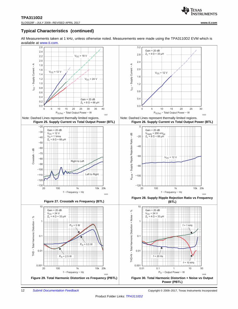
Note: Dashed Lines represent thermally limited regions.Figure 25. Supply Current vs Total Output Power (BTL)
Note: Dashed Lines represent thermally limited regions.Figure 26. Supply Current vs Total Output Power (BTL)
SPACEFigure 27. Crosstalk vs Frequency (BTL)
Figure 28. Supply Ripple Rejection Ratio vs Frequency(BTL)
Figure 29. Total Harmonic Distortion vs Frequency (PBTL) Figure 30. Total Harmonic Distortion + Noise vs OutputPower (PBTL)

−120
−100
−80
−60
−40
−20
0
f − Frequency − Hz
KS
VR
−S
upply
Rip
ple
Reje
ction
Ratio
−dB
20 100 1k 10k 20k
G031
Gain = 20 dB
Vripple = 200 mVpp
ZL = 8 Ω + 66 µH
VCC = 12 V
PO − Output Power − W
0
10
20
30
40
50
60
70
80
90
100
0 5 10 15 20 25 30 35 40 45
h−
Effi
cie
ncy
−%
G029
Gain = 20 dB
ZL = 4 Ω + 33 µH
VCC = 12 V
VCC = 18 V
PO − Output Power − W
0.0
0.2
0.4
0.6
0.8
1.0
1.2
1.4
1.6
1.8
2.0
2.2
2.4
2.6
2.8
0 5 10 15 20 25 30 35 40 45
I CC
−S
upply
Curr
ent−
A
G030
VCC = 12 V
Gain = 20 dB
ZL = 4 Ω + 33 µH
VCC = 18 V
f − Frequency − HzP
hase
−°
100
50
0
−3000
5
10
15
20
25
30
35
40
Gain
−dB
−50
−100
−150
20 100 10k 100k1k
G027
Phase
Gain
−200
−250
CI = 1 µF
Gain = 20 dB
Filter = Audio Precision AUX-0025
VCC = 24 V
VI = 0.1 Vrms
ZL = 8 Ω + 66 µH
Vcc - Supply Voltage - V
Po
- O
utpu
t Pow
er -
W
6 8 10 12 14 16 18 20 22 240
5
10
15
20
25
30
35
40
45
50
55
Gain = 20 dBZL = 4 : + 33PH
THD= 1%
THD = 10%
13
TPA3110D2www.ti.com SLOS528F –JULY 2009–REVISED APRIL 2017
Product Folder Links: TPA3110D2
Submit Documentation FeedbackCopyright © 2009–2017, Texas Instruments Incorporated
Typical Characteristics (continued)All Measurements taken at 1 kHz, unless otherwise noted. Measurements were made using the TPA3110D2 EVM which isavailable at www.ti.com.
Figure 31. Gain and Phase vs Frequency (PBTL)The figure is measured with heatsink(1) on EVM(2)
Figure 32. Output Power vs Supply Voltage (PBTL)
SPACEFigure 33. Efficiency vs Output Power (PBTL)
Figure 34. Supply Current vs Output Power (PBTL)
Figure 35. Supply Ripple Rejection Ratio vs Frequency (PBTL)

PWM
Logic
Gate
Drive
Gate
Drive
PVCCL
PVCCL
GVDD
PVCCL
PVCCL
BSPL
PGND
OUTPL
OUTNL
PGND
GVDD
BSNL
PWM
Logic
Gate
Drive
Gate
Drive
PVCCL
PVCCL
GVDD
PVCCL
PVCCL
BSNR
PGND
OUTNR
OUTPR
PGND
GVDD
BSPR
LINP
LINN
RINP
RINN
UVLO/OVLO
SC Detect
DC Detect
Thermal
Detect
Startup Protection
Logic
Biases and
References
FAULT
SD
GAIN0
PLIMIT
AGND
AVCC
GAIN1
Gain
Control
TTL
Buffer
Ramp
Generator
AVDD
GVDD
GVDD
LDO
Regulator
Gain
ControlPLIMIT
PLIMIT
Reference
PBTL
Gain
Control
TTL
BufferPBTL
Select
PBTL Select
PBTL Select
OUTPL FB
OUTNL FB
OUTNN FB
OUTNP FB
OUTPR FB
OUTNR FB
OUTNL FB
OUTPL FB
PLIMIT
14
TPA3110D2SLOS528F –JULY 2009–REVISED APRIL 2017 www.ti.com
Product Folder Links: TPA3110D2
Submit Documentation Feedback Copyright © 2009–2017, Texas Instruments Incorporated
(1) Detailed parameters of heatsink: please refer to datasheet heatsink with part number ATS-TI10P-521-C1-R1.(2) Related parameters of the two-layer EVM: copper thickness of top layer and bottom layer are both 0.03556mm.
8 Parameter Measurement InformationAll parameters are measured according to the conditions described in the Specifications section.
9 Detailed Description
9.1 OverviewThe TPA3110D2 is a 15-W Class-D audio power amplifier. It is designed to drive BTL stereo speakers. Thisdevice is able to use inexpensive ferrite bead filters at the outputs while meeting EMC requirements. TheTPA3110D2 can drive stereo speakers as low as 4 Ω and its high efficiency eliminates the need for an externalheat sink. The device is fully protected against shorts to GND, VCC and output-to-output. The short-circuitprotection and thermal protection includes an auto-recovery feature.
9.2 Functional Block Diagram

OUTP
OUTN
OUTP
Speaker
Current
OUTP
OUTN
OUTP-OUTN
Speaker
Current
OUTP
OUTN
OUTP-OUTN
Speaker
Current
0V
0V
PVCC
No Output
Positive Output
Negative Output
0A
0A
0V
-PVCC
OUTP-OUTN
15
TPA3110D2www.ti.com SLOS528F –JULY 2009–REVISED APRIL 2017
Product Folder Links: TPA3110D2
Submit Documentation FeedbackCopyright © 2009–2017, Texas Instruments Incorporated
9.3 Feature Description
9.3.1 TPA3110D2 Modulation SchemeThe TPA3110D2 uses a modulation scheme that allows operation without the classic LC reconstruction filterwhen the amp is driving an inductive load. Each output is switching from 0 volts to the supply voltage. The OUTPand OUTN are in phase with each other with no input so that there is little or no current in the speaker. The dutycycle of OUTP is greater than 50% and OUTN is less than 50% for positive output voltages. The duty cycle ofOUTP is less than 50% and OUTN is greater than 50% for negative output voltages. The voltage across the loadsits at 0V throughout most of the switching period, reducing the switching current, which reduces any I2R lossesin the load.
Figure 36. The TPA3110D2 Output Voltage And Current Waveforms Into An Inductive Load
9.3.1.1 Ferrite Bead Filter ConsiderationsUsing the Advanced Emissions Suppression Technology in the TPA3110D2 amplifier it is possible to design ahigh efficiency Class-D audio amplifier while minimizing interference to surrounding circuits. It is also possible toaccomplish this with only a low-cost ferrite bead filter. In this case it is necessary to carefully select the ferritebead used in the filter.
One important aspect of the ferrite bead selection is the type of material used in the ferrite bead. Not all ferritematerial is alike, so it is important to select a material that is effective in the 10 to 100 MHz range which is key tothe operation of the Class D amplifier. Many of the specifications regulating consumer electronics haveemissions limits as low as 30 MHz. It is important to use the ferrite bead filter to block radiation in the 30 MHzand above range from appearing on the speaker wires and the power supply lines which are good antennas forthese signals. The impedance of the ferrite bead can be used along with a small capacitor with a value in therange of 1000 pF to reduce the frequency spectrum of the signal to an acceptable level. For best performance,the resonant frequency of the ferrite bead/ capacitor filter should be less than 10 MHz.

FCC Class B
f - Frequency - Hz
830M
Lim
it L
evel -
dB
V/m
m
30M
20
230M 430M 630M
0
40
10
60
30
70
50
16
TPA3110D2SLOS528F –JULY 2009–REVISED APRIL 2017 www.ti.com
Product Folder Links: TPA3110D2
Submit Documentation Feedback Copyright © 2009–2017, Texas Instruments Incorporated
Feature Description (continued)Also, it is important that the ferrite bead is large enough to maintain its impedance at the peak currents expectedfor the amplifier. Some ferrite bead manufacturers specify the bead impedance at a variety of current levels. Inthis case it is possible to make sure the ferrite bead maintains an adequate amount of impedance at the peakcurrent the amplifier will see. If these specifications are not available, it is also possible to estimate the beadcurrent handling capability by measuring the resonant frequency of the filter output at low power and at maximumpower. A change of resonant frequency of less than fifty percent under this condition is desirable. Examples offerrite beads which have been tested and work well with the TPA3110D2 include 28L0138-80R-10 andHI1812V101R-10 from Steward and the 742792510 from Wurth Electronics.
A high quality ceramic capacitor is also needed for the ferrite bead filter. A low ESR capacitor with goodtemperature and voltage characteristics will work best.
Additional EMC improvements may be obtained by adding snubber networks from each of the class D outputs toground. Suggested values for a simple RC series snubber network would be 10 Ω in series with a 330 pFcapacitor although design of the snubber network is specific to every application and must be designed takinginto account the parasitic reactance of the printed circuit board as well as the audio amp. Take care to evaluatethe stress on the component in the snubber network especially if the amp is running at high PVCC. Also, makesure the layout of the snubber network is tight and returns directly to the PGND or the PowerPAD™ beneath thechip.
Figure 37. TPA3110D2 EMC Spectrum With FCC Class B Limits
9.3.1.2 Efficiency: LC Filter Required With The Traditional Class-D Modulation SchemeThe main reason that the traditional class-D amplifier needs an output filter is that the switching waveform resultsin maximum current flow. This causes more loss in the load, which causes lower efficiency. The ripple current islarge for the traditional modulation scheme, because the ripple current is proportional to voltage multiplied by thetime at that voltage. The differential voltage swing is 2 × VCC, and the time at each voltage is half the period forthe traditional modulation scheme. An ideal LC filter is needed to store the ripple current from each half cycle forthe next half cycle, while any resistance causes power dissipation. The speaker is both resistive and reactive,whereas an LC filter is almost purely reactive.
The TPA3110D2 modulation scheme has little loss in the load without a filter because the pulses are short andthe change in voltage is VCC instead of 2 × VCC. As the output power increases, the pulses widen, making theripple current larger. Ripple current could be filtered with an LC filter for increased efficiency, but for mostapplications the filter is not needed.
An LC filter with a cutoff frequency less than the class-D switching frequency allows the switching current to flowthrough the filter instead of the load. The filter has less resistance but higher impedance at the switchingfrequency than the speaker, which results in less power dissipation, therefore increasing efficiency.

1 nF
Ferrite
Chip Bead
OUTP
OUTN
Ferrite
Chip Bead
1 nF
2.2 mF
15 Hm
15 mH
OUTP
OUTN
L1
L2
C2
C3
2.2 mF
1 mF
1 mF
33 Hm
33 mH
OUTP
OUTN
L1
L2
C2
C3
17
TPA3110D2www.ti.com SLOS528F –JULY 2009–REVISED APRIL 2017
Product Folder Links: TPA3110D2
Submit Documentation FeedbackCopyright © 2009–2017, Texas Instruments Incorporated
Feature Description (continued)9.3.1.3 When to Use an Output Filter for EMI SuppressionThe TPA3110D2 has been tested with a simple ferrite bead filter for a variety of applications including longspeaker wires up to 125 cm and high power. The TPA3110D2 EVM passes FCC Class B specifications underthese conditions using twisted speaker wires. The size and type of ferrite bead can be selected to meetapplication requirements. Also, the filter capacitor can be increased if necessary with some impact on efficiency.
There may be a few circuit instances where it is necessary to add a complete LC reconstruction filter. Thesecircumstances might occur if there are nearby circuits which are sensitive to noise. In these cases a classicsecond order Butterworth filter similar to those shown in the figures below can be used.
Some systems have little power supply decoupling from the AC line but are also subject to line conductedinterference (LCI) regulations. These include systems powered by "wall warts" and "power bricks." In thesecases, it LC reconstruction filters can be the lowest cost means to pass LCI tests. Common mode chokes usinglow frequency ferrite material can also be effective at preventing line conducted interference.
Figure 38. Typical LC Output Filter, Cutoff Frequency of 27 Khz, Speaker Impedance = 8 Ω
Figure 39. Typical Lc Output Filter, Cutoff Frequency Of 27 Khz, Speaker Impedance = 4 Ω
Figure 40. Typical Ferrite Chip Bead Filter (Chip Bead Example)
9.3.2 Gain Setting Via GAIN0 And GAIN1 InputsThe gain of the TPA3110D2 is set by two input terminals, GAIN0 and GAIN1. The voltage slew rate of these gainterminals, along with terminals 1 and 14, must be restricted to no more than 10V/ms. For higher slew rates, usea 100kΩ resistor in series with the terminals.

TPA3110D2 Power Limit FunctionVin=1.13 Freq=1kHz RLoad=8WVPP
PLIMIT = 1.8V Pout = 5W
PLIMIT = 3V Pout = 10W
PLIMIT = 6.96V Pout = 11.8W
Vinput
18
TPA3110D2SLOS528F –JULY 2009–REVISED APRIL 2017 www.ti.com
Product Folder Links: TPA3110D2
Submit Documentation Feedback Copyright © 2009–2017, Texas Instruments Incorporated
Feature Description (continued)The gains listed in Table 2 are realized by changing the taps on the input resistors and feedback resistors insidethe amplifier. This causes the input impedance (ZI) to be dependent on the gain setting. The actual gain settingsare controlled by ratios of resistors, so the gain variation from part-to-part is small. However, the input impedancefrom part-to-part at the same gain may shift by ±20% due to shifts in the actual resistance of the input resistors.
For design purposes, the input network (discussed in the next section) should be designed assuming an inputimpedance of 7.2 kΩ, which is the absolute minimum input impedance of the TPA3110D2. At the lower gainsettings, the input impedance could increase as high as 72 kΩ
Table 2. Gain Setting
GAIN1 GAIN0AMPLIFIER GAIN (dB) INPUT IMPEDANCE
(kΩ)TYP TYP
0 0 20 600 1 26 301 0 32 151 1 36 9
9.3.3 Differential InputsThe differential input stage of the amplifier cancels any noise that appears on both input lines of the channel. Touse the TPA3110D2 with a differential source, connect the positive lead of the audio source to the INP input andthe negative lead from the audio source to the INN input. To use the TPA3110D2 with a single-ended source, acground the INP or INN input through a capacitor equal in value to the input capacitor on INN or INP and applythe audio source to either input. In a single-ended input application, the unused input should be ac grounded atthe audio source instead of at the device input for best noise performance. For good transient performance, theimpedance seen at each of the two differential inputs should be the same.
The impedance seen at the inputs should be limited to an RC time constant of 1 ms or less if possible. This is toallow the input dc blocking capacitors to become completely charged during the 14 ms power-up time. If the inputcapacitors are not allowed to completely charge, there will be some additional sensitivity to component matchingwhich can result in pop if the input components are not well matched.
9.3.4 PLIMITThe voltage at pin 10 can used to limit the power to levels below that which is possible based on the supply rail.Add a resistor divider from GVDD to ground to set the voltage at the PLIMIT pin. An external reference may alsobe used if tighter tolerance is required. Also add a 1μF capacitor from pin 10 to ground.
Figure 41. PLIMIT Circuit Operation

LP
L S
OUTL
2R
x VR + 2 x R
P = for unclipped power2 x R
æ öæ öç ÷ç ÷ç ÷è øè ø
19
TPA3110D2www.ti.com SLOS528F –JULY 2009–REVISED APRIL 2017
Product Folder Links: TPA3110D2
Submit Documentation FeedbackCopyright © 2009–2017, Texas Instruments Incorporated
The PLIMIT circuit sets a limit on the output peak-to-peak voltage. The limiting is done by limiting the duty cycleto fixed maximum value. This limit can be thought of as a virtual voltage rail which is lower than the supplyconnected to PVCC. This "virtual" rail is 4 times the voltage at the PLIMIT pin. This output voltage can be used tocalculate the maximum output power for a given maximum input voltage and speaker impedance.
Where:• RS is the total series resistance including RDS(on), and any resistance in the output filter.• RL is the load resistance.• VP is the peak amplitude of the output possible within the supply rail.• POUT (10%THD) = 1.25 × POUT (unclipped) (1)
Table 3. PLIMIT Typical Operation
TEST CONDITIONS PLIMIT VOLTAGE OUTPUT POWER (W) OUTPUT VOLTAGEAMPLITUDE (VP-P)
PVCC=24V, Vin=1Vrms,RL=8Ω, Gain=26dB
6.97 36.1 (thermally limited) 43
PVCC=24V, Vin=1Vrms,RL=8Ω, Gain=26dB
2.94 15 25.2
PVCC=24V, Vin=1Vrms,RL=8Ω, Gain=26dB
2.34 10 20
PVCC=24V, Vin=1Vrms,RL=8Ω, Gain=26dB
1.62 5 14
PVCC=24V, Vin=1Vrms,RL=8Ω, Gain=20dB
6.97 12.1 27.7
PVCC=24V, Vin=1Vrms,RL=8Ω, Gain=20dB
3.00 10 23
PVCC=24V, Vin=1Vrms,RL=8Ω, Gain=20dB
1.86 5 14.8
PVCC=12V, Vin=1Vrms,RL=8Ω, Gain=20dB
6.97 10.55 23.5
PVCC=12V, Vin=1Vrms,RL=8Ω, Gain=20dB
1.76 5 15
9.3.5 GVDD SupplyThe GVDD Supply is used to power the gates of the output full bridge transistors. It can also be used to supplythe PLIMIT voltage divider circuit. Add a 1-μF capacitor to ground at this pin.
9.3.6 PBTL SelectTPA3110D2 offers the feature of parallel BTL operation with two outputs of each channel connected directly. Ifthe PBTL pin (pin 14) is tied high, the positive and negative outputs of each channel (left and right) aresynchronized and in phase. To operate in this PBTL (mono) mode, apply the input signal to the RIGHT input andplace the speaker between the LEFT and RIGHT outputs. Connect the positive and negative output together forbest efficiency. The voltage slew rate of the PBTL pin must be restricted to no more than 10V/ms. For higherslew rates, use a 100kΩ resistor in series with the terminals. For an example of the PBTL connection, see theschematic in the APPLICATION INFORMATION section.
For normal BTL operation, connect the PBTL pin to local ground.

20
TPA3110D2SLOS528F –JULY 2009–REVISED APRIL 2017 www.ti.com
Product Folder Links: TPA3110D2
Submit Documentation Feedback Copyright © 2009–2017, Texas Instruments Incorporated
9.3.7 Thermal ProtectionThermal protection on the TPA3110D2 prevents damage to the device when the internal die temperatureexceeds 150°C. There is a ±15°C tolerance on this trip point from device to device. Once the die temperatureexceeds the thermal set point, the device enters into the shutdown state and the outputs are disabled. This is nota latched fault. The thermal fault is cleared once the temperature of the die is reduced by 15°C. The devicebegins normal operation at this point with no external system interaction.
Thermal protection faults are NOT reported on the FAULT terminal.
9.3.8 DC DetectTPA3110D2 has circuitry which will protect the speakers from DC current which might occur due to defectivecapacitors on the input or shorts on the printed circuit board at the inputs. A DC detect fault will be reported onthe FAULT pin as a low state. The DC Detect fault will also cause the amplifier to shutdown by changing thestate of the outputs to Hi-Z. To clear the DC Detect it is necessary to cycle the PVCC supply. Cycling S D willNOT clear a DC detect fault.
A DC Detect Fault is issued when the output differential duty-cycle of either channel exceeds 14% (for example,+57%, -43%) for more than 420 msec at the same polarity. This feature protects the speaker from large DCcurrents or AC currents less than 2Hz. To avoid nuisance faults due to the DC detect circuit, hold the SD pin lowat power-up until the signals at the inputs are stable. Also, take care to match the impedance seen at the positiveand negative inputs to avoid nuisance DC detect faults.
The minimum differential input voltages required to trigger the DC detect are show in table 2. The inputs mustremain at or above the voltage listed in the table for more than 420 msec to trigger the DC detect.
Table 4. DC Detect ThresholdAV(dB) Vin (mV, differential)
20 11226 5632 2836 17
9.3.9 Short-Circuit Protection and Automatic Recovery FeatureTPA3110D2 has protection from overcurrent conditions caused by a short circuit on the output stage. The shortcircuit protection fault is reported on the FAULT pin as a low state. The amplifier outputs are switched to a Hi-Zstate when the short circuit protection latch is engaged. The latch can be cleared by cycling the SD pin throughthe low state.
If automatic recovery from the short circuit protection latch is desired, connect the FAULT pin directly to the SDpin. This allows the FAULT pin function to automatically drive the SD pin low which clears the short-circuitprotection latch.
9.4 Device Functional Modes
9.4.1 SD OperationThe TPA3110D2 employs a shutdown mode of operation designed to reduce supply current (ICC) to the absoluteminimum level during periods of nonuse for power conservation. The SD input terminal should be held high (seespecification table for trip point) during normal operation when the amplifier is in use. Pulling SD low causes theoutputs to mute and the amplifier to enter a low-current state. Never leave SD unconnected, because amplifieroperation would be unpredictable.
For the best power-off pop performance, place the amplifier in the shutdown mode prior to removing the powersupply voltage.

PVCC
PVCC
GAIN16
AVCC7
8AGND
9GVDD
OUTNL
BSNL
BSNR
OUTNR
23
22
21
20
TPA3110D2
FAULT2
LINP3
4LINN
5GAIN0
PVCCL
BSPL
OUTPL
PGND
27
26
25
24
PLIMIT10
RINN11
12RINP
13NC
PGND
OUTPR
BSPR
PVCCR
19
18
17
16
PBTL14
PVCCR15
GND
29PowerPAD
SD1
PVCCL28
PVCC
100 μF 0.1 μF 1000 pF
100 μF 0.1 μF 1000 pF
Audio
Source
Control
System
100 kΩ
10 Ω
1 kΩ
FB
FB
0.22 μF
1000 pF
0.22 μF
1000 pF
1 Fm
1 Fm
0.22 μF
FB
FB
1000 pF
1000 pF
0.22 μF
10 kΩ
10 kΩ
1 Fm
1 Fm
1 Fm
1 Fm
1 Fm
21
TPA3110D2www.ti.com SLOS528F –JULY 2009–REVISED APRIL 2017
Product Folder Links: TPA3110D2
Submit Documentation FeedbackCopyright © 2009–2017, Texas Instruments Incorporated
10 Application and Implementation
NOTEInformation in the following applications sections is not part of the TI componentspecification, and TI does not warrant its accuracy or completeness. TI’s customers areresponsible for determining suitability of components for their purposes. Customers shouldvalidate and test their design implementation to confirm system functionality.
10.1 Application InformationThis section describes a stereo BTL application and a mono PBTL application. In the stereo application thePower Limiter is implemented, however in the mono application this limiter is not used.
10.2 Typical Applications
10.2.1 Stereo Class-D Amplifier With BTL Output and Single-Ended Inputs With Power Limiting
Figure 42. Typical Application Schematic With BTL Output and Single-Ended Inputs With Power Limiting

C =i
1
2 Z fpi c
f =c
1
2 Z Cpi i
-3 dB
fc
f =1
2 Z Cpi i
Ci
INZi
Zf
Input
Signal
22
TPA3110D2SLOS528F –JULY 2009–REVISED APRIL 2017 www.ti.com
Product Folder Links: TPA3110D2
Submit Documentation Feedback Copyright © 2009–2017, Texas Instruments Incorporated
Typical Applications (continued)10.2.1.1 Design RequirementsFor this design example, use the parameters listed in Table 5.
Table 5. Design ParametersDESIGN PARAMETER EXAMPLE VALUE
Power supply 8 V to 26 V
Shutdown, gain, and PBTL controlsHigh > 2 V
Low < 0.8 VSpeaker impedance BTL 4 to 8 Ω
Speaker impedance PBTL 2 to 8 Ω
10.2.1.2 Detailed Design Procedure
10.2.1.2.1 Input Resistance
Changing the gain setting can vary the input resistance of the amplifier from its smallest value, 9 kΩ ±20%, to thelargest value, 60 kΩ ±20%. As a result, if a single capacitor is used in the input high-pass filter, the –3 dB orcutoff frequency may change when changing gain steps.
Figure 43. Input Impedance of the TPA3110D2
The –3-dB frequency can be calculated using Equation 2. Use the ZI values given in Table 2.
(2)
10.2.1.2.2 Input Capacitor, CI
In the typical application, an input capacitor (CI) is required to allow the amplifier to bias the input signal to theproper dc level for optimum operation. In this case, CI and the input impedance of the amplifier (ZI) form a high-pass filter with the corner frequency determined in Equation 3.
(3)
The value of CI is important, as it directly affects the bass (low-frequency) performance of the circuit. Considerthe example where ZI is 60 kΩ and the specification calls for a flat bass response down to 20 Hz. Equation 3 isreconfigured as Equation 4.
(4)

VCC − Supply Voltage − V
0
5
10
15
20
25
30
6 8 10 12 14 16 18 20 22 24 26
PO
−O
utp
ut
Pow
er
−W
G016
THD = 10%
THD = 1%
Gain = 20 dB
ZL = 8 Ω + 66 µH
VCC − Supply Voltage − V
0
5
10
15
20
25
6 8 10 12 14 16 18
PO
−O
utp
ut
Pow
er
−W
G017
THD = 10%
THD = 1%
Gain = 20 dB
ZL = 4 Ω + 33 µH
23
TPA3110D2www.ti.com SLOS528F –JULY 2009–REVISED APRIL 2017
Product Folder Links: TPA3110D2
Submit Documentation FeedbackCopyright © 2009–2017, Texas Instruments Incorporated
In this example, CI is 0.13 µF; so, one would likely choose a value of 0.15 μF as this value is commonly used. Ifthe gain is known and is constant, use ZI from Table 2 to calculate CI. A further consideration for this capacitor isthe leakage path from the input source through the input network (CI) and the feedback network to the load. Thisleakage current creates a dc offset voltage at the input to the amplifier that reduces useful headroom, especiallyin high gain applications. For this reason, a low-leakage tantalum or ceramic capacitor is the best choice. Whenpolarized capacitors are used, the positive side of the capacitor should face the amplifier input in mostapplications as the dc level there is held at 3 V, which is likely higher than the source dc level. Note that it isimportant to confirm the capacitor polarity in the application. Additionally, lead-free solder can create dc offsetvoltages and it is important to ensure that boards are cleaned properly.
10.2.1.2.3 BSN and BSP Capacitors
The full H-bridge output stages use only NMOS transistors. Therefore, they require bootstrap capacitors for thehigh side of each output to turn on correctly. A 0.22 μF ceramic capacitor, rated for at least 25 V, must beconnected from each output to its corresponding bootstrap input. Specifically, one 0.22 μF capacitor must beconnected from OUTPx to BSPx, and one 0.22 μF capacitor must be connected from OUTNx to BSNx. (See theapplication circuit diagram in Figure 42.)
The bootstrap capacitors connected between the BSxx pins and corresponding output function as a floatingpower supply for the high-side N-channel power MOSFET gate drive circuitry. During each high-side switchingcycle, the bootstrap capacitors hold the gate-to-source voltage high enough to keep the high-side MOSFETsturned on.
10.2.1.2.4 Using Low-ESR Capacitors
Low-ESR capacitors are recommended throughout this application section. A real (as opposed to ideal) capacitorcan be modeled simply as a resistor in series with an ideal capacitor. The voltage drop across this resistorminimizes the beneficial effects of the capacitor in the circuit. The lower the equivalent value of this resistance,the more the real capacitor behaves like an ideal capacitor.
10.2.1.3 Application Curves
Note: Dashed Lines represent thermally limited regions.Figure 44. Output Power vs Supply Voltage (BTL)
Note: Dashed Lines represent thermally limited regions.Figure 45. Output Power vs Supply Voltage (BTL)

PVCC
PVCC
GAIN16
AVCC7
8AGND
9GVDD
23
22
21
20
TPA3110D2
FAULT2
LINP3
4LINN
5GAIN0
27
26
25
24
PLIMIT10
RINN11
12RINP
13NC
19
18
17
16
PBTL14 15
GND
29PowerPAD
SD1 28
PVCC
100 μF 0.1 μF 1000 pF
100 μF 0.1 μF 1000 pF
Audio
Source
Control
System
100 kΩ
10
100 kW(1)
Ω
1 kΩ
FB
FB
0.47 μF
1000 pF
0.47 μF
1000 pF
AVCC
1 Fm
1 Fm
1 Fm
1 Fm
OUTNL
BSNL
BSNR
OUTNR
PVCCL
BSPL
OUTPL
PGND
PGND
OUTPR
BSPR
PVCCR
PVCCR
PVCCL
AVCC
24
TPA3110D2SLOS528F –JULY 2009–REVISED APRIL 2017 www.ti.com
Product Folder Links: TPA3110D2
Submit Documentation Feedback Copyright © 2009–2017, Texas Instruments Incorporated
10.2.2 Stereo Class-D Amplifier With PBTL Output and Single-Ended Input
(1) 100 kΩ resistor is needed if the PVCC slew rate is more than 10 V/ms.
Figure 46. Typical Application Schematic With PBTL Output and Single-Ended Input
10.2.2.1 Design RequirementsRefer to Table 5 for the Stereo Class-D Amplifier With PBTL Output and Single-Ended Input Application DesignRequirements.
10.2.2.2 Detailed Design ProcedureRefer to Detailed Design Procedure for the Stereo Class-D Amplifier With PBTL Output and Single-Ended InputApplication Detailed Design Procedure.
VCC − Supply Voltage − V
0
5
10
15
20
25
30
35
40
6 8 10 12 14 16 18 20
PO
−O
utp
ut
Pow
er
−W
G028
THD = 10%
THD = 1%
Gain = 20 dB
ZL = 4 Ω + 33 µH
25
TPA3110D2www.ti.com SLOS528F –JULY 2009–REVISED APRIL 2017
Product Folder Links: TPA3110D2
Submit Documentation FeedbackCopyright © 2009–2017, Texas Instruments Incorporated
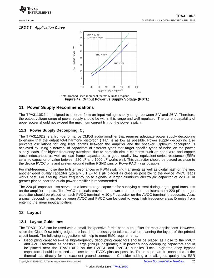
10.2.2.3 Application Curve
Note: Dashed Lines represent thermally limited regions.Figure 47. Output Power vs Supply Voltage (PBTL)
11 Power Supply RecommendationsThe TPA3110D2 is designed to operate form an input voltage supply range between 8-V and 26-V. Therefore,the output voltage range of power supply should be within this range and well regulated. The current capability ofupper power should not exceed the maximum current limit of the power switch.
11.1 Power Supply Decoupling, CS
The TPA3110D2 is a high-performance CMOS audio amplifier that requires adequate power supply decouplingto ensure that the output total harmonic distortion (THD) is as low as possible. Power supply decoupling alsoprevents oscillations for long lead lengths between the amplifier and the speaker. Optimum decoupling isachieved by using a network of capacitors of different types that target specific types of noise on the powersupply leads. For higher frequency transients due to parasitic circuit elements such as bond wire and coppertrace inductances as well as lead frame capacitance, a good quality low equivalent-series-resistance (ESR)ceramic capacitor of value between 220 pF and 1000 pF works well. This capacitor should be placed as close tothe device PVCC pins and system ground (either PGND pins or PowerPAD™) as possible.
For mid-frequency noise due to filter resonances or PWM switching transients as well as digital hash on the line,another good quality capacitor typically 0.1 μF to 1 µF placed as close as possible to the device PVCC leadsworks best. For filtering lower frequency noise signals, a larger aluminum electrolytic capacitor of 220 μF orgreater placed near the audio power amplifier is recommended.
The 220-μF capacitor also serves as a local storage capacitor for supplying current during large signal transientson the amplifier outputs. The PVCC terminals provide the power to the output transistors, so a 220 µF or largercapacitor should be placed on each PVCC terminal. A 10-µF capacitor on the AVCC terminal is adequate. Also,a small decoupling resistor between AVCC and PVCC can be used to keep high frequency class D noise fromentering the linear input amplifiers.
12 Layout
12.1 Layout GuidelinesThe TPA3110D2 can be used with a small, inexpensive ferrite bead output filter for most applications. However,since the Class-D switching edges are fast, it is necessary to take care when planning the layout of the printedcircuit board. The following suggestions will help to meet EMC requirements.• Decoupling capacitors—The high-frequency decoupling capacitors should be placed as close to the PVCC
and AVCC terminals as possible. Large (220 µF or greater) bulk power supply decoupling capacitors shouldbe placed near the TPA3110D2 on the PVCCL and PVCCR supplies. Local, high-frequency bypasscapacitors should be placed as close to the PVCC pins as possible. These caps can be connected to thethermal pad directly for an excellent ground connection. Consider adding a small, good quality low ESR

LINP
LINN
FAULT
GAIN0
GAIN1
PLIMIT
RINN
RINP
PBTL
FB
FB
FB
FB
OUTPL
OUTNL
FBOUTNR
FBOUTPR
`
Top Layer Ground Plane
Vias on the thermal pad to get optimal thermal performance
1 µF
1 nF 100 µF0.1 nF
1 nF 100 µF0.1 nF
1 nF
1 nF
1 nF
1 nF
330 pF
330 pF
0.22 µF
0.22 µF
0.22 µF
0.22 µF
330 pF
330 pF
10
SD
10
10
10
1 µF
1 µF
1 µF
1 µF
1 µF
Place Decoupling capacitors as close to the device as possible.
Place Decoupling capacitors as close to the device as possible.
Several Via connection between top and
bottom ground layers for EMI and Thermal
performance
Bulk Capacitor for good audio decoupling close to
Power source
Pad to Top Layer Ground Plane
Top Layer Traces
PowerPAD
Via to Ground Plane Via to Power
26
TPA3110D2SLOS528F –JULY 2009–REVISED APRIL 2017 www.ti.com
Product Folder Links: TPA3110D2
Submit Documentation Feedback Copyright © 2009–2017, Texas Instruments Incorporated
Layout Guidelines (continued)ceramic capacitor between 220 pF and 1000 pF and a larger mid-frequency cap of value between 0.1μF and1μF also of good quality to the PVCC connections at each end of the chip.
• Keep the current loop from each of the outputs through the ferrite bead and the small filter cap and back toPGND as small and tight as possible. The size of this current loop determines its effectiveness as anantenna.
• Grounding—The AVCC (pin 7) decoupling capacitor should be grounded to analog ground (AGND). ThePVCC decoupling capacitors should connect to PGND. Analog ground and power ground should beconnected at the thermal pad, which should be used as a central ground connection or star ground for theTPA3110D2.
• Output filter—The ferrite EMI filter (Figure 40) should be placed as close to the output terminals as possiblefor the best EMI performance. The LC filter (Figure 38 and Figure 39) should be placed close to the outputs.The capacitors used in both the ferrite and LC filters should be grounded to power ground.
• Thermal Pad—The thermal pad must be soldered to the PCB for proper thermal performance and optimalreliability. The dimensions of the thermal pad and thermal land should be 6.46mm by 2.35mm. Seven rows ofsolid vias (three vias per row, 0,3302 mm or 13 mils diameter) should be equally spaced underneath thethermal land. The vias should connect to a solid copper plane, either on an internal layer or on the bottomlayer of the PCB. The vias must be solid vias, not thermal relief or webbed vias. See the TI ApplicationReport SLMA002 for more information about using the TSSOP thermal pad. For recommended PCBfootprints, see figures at the end of this data sheet.
For an example layout, see the TPA3110D2 Evaluation Module (TPA3110D2EVM) User Manual. Both the EVMuser manual and the thermal pad application report are available on the TI Web site at www.ti.com.
12.2 Layout Example
Figure 48. TPA3110D2 PCB Layout

27
TPA3110D2www.ti.com SLOS528F –JULY 2009–REVISED APRIL 2017
Product Folder Links: TPA3110D2
Submit Documentation FeedbackCopyright © 2009–2017, Texas Instruments Incorporated
13 Device and Documentation Support
13.1 Device Support
13.1.1 Development SupportFor the TPA3110D2 TINA-TI Reference Design, see SLAM052
For the TPA3110D2 TINA-TI Spice Model, see SLAM053
13.2 Documentation Support
13.2.1 Related DocumentationFor related documentation see the following:• Application Report, PowerPAD™ Thermally Enhanced Package, SLMA002• Application Report, Using Thermal Calculation Tools for Analog Components, SLUA566• Application Report, AN-1737 Managing EMI in Class D Audio Applications, SNAA050• Application Report, AN-1849 An Audio Amplifier Power Supply Design, SNAA057• Application Report, Guidelines for Measuring Audio Power Amplifier Performance, SLOA068• User's Guide, TPA3110D2 EVM Audio Amplifier Evaluation Board SLOU263
13.3 Community ResourcesThe following links connect to TI community resources. Linked contents are provided "AS IS" by the respectivecontributors. They do not constitute TI specifications and do not necessarily reflect TI's views; see TI's Terms ofUse.
TI E2E™ Online Community TI's Engineer-to-Engineer (E2E) Community. Created to foster collaborationamong engineers. At e2e.ti.com, you can ask questions, share knowledge, explore ideas and helpsolve problems with fellow engineers.
Design Support TI's Design Support Quickly find helpful E2E forums along with design support tools andcontact information for technical support.
13.4 TrademarksSpeakerGuard, PowerPAD, E2E are trademarks of Texas Instruments.All other trademarks are the property of their respective owners.
13.5 Electrostatic Discharge CautionThese devices have limited built-in ESD protection. The leads should be shorted together or the device placed in conductive foamduring storage or handling to prevent electrostatic damage to the MOS gates.
13.6 GlossarySLYZ022 — TI Glossary.
This glossary lists and explains terms, acronyms, and definitions.
14 Mechanical, Packaging, and Orderable InformationThe following pages include mechanical, packaging, and orderable information. This information is the mostcurrent data available for the designated devices. This data is subject to change without notice and revision ofthis document. For browser-based versions of this data sheet, refer to the left-hand navigation.
PACKAGE OPTION ADDENDUM
www.ti.com 10-Dec-2020
Addendum-Page 1
PACKAGING INFORMATION
Orderable Device Status(1)
Package Type PackageDrawing
Pins PackageQty
Eco Plan(2)
Lead finish/Ball material
(6)
MSL Peak Temp(3)
Op Temp (°C) Device Marking(4/5)
Samples
TPA3110D2PWP ACTIVE HTSSOP PWP 28 50 RoHS & Green NIPDAU Level-3-260C-168 HR -40 to 85 TPA3110D2
TPA3110D2PWPR ACTIVE HTSSOP PWP 28 2000 RoHS & Green NIPDAU Level-3-260C-168 HR -40 to 85 TPA3110D2
(1) The marketing status values are defined as follows:ACTIVE: Product device recommended for new designs.LIFEBUY: TI has announced that the device will be discontinued, and a lifetime-buy period is in effect.NRND: Not recommended for new designs. Device is in production to support existing customers, but TI does not recommend using this part in a new design.PREVIEW: Device has been announced but is not in production. Samples may or may not be available.OBSOLETE: TI has discontinued the production of the device.
(2) RoHS: TI defines "RoHS" to mean semiconductor products that are compliant with the current EU RoHS requirements for all 10 RoHS substances, including the requirement that RoHS substancedo not exceed 0.1% by weight in homogeneous materials. Where designed to be soldered at high temperatures, "RoHS" products are suitable for use in specified lead-free processes. TI mayreference these types of products as "Pb-Free".RoHS Exempt: TI defines "RoHS Exempt" to mean products that contain lead but are compliant with EU RoHS pursuant to a specific EU RoHS exemption.Green: TI defines "Green" to mean the content of Chlorine (Cl) and Bromine (Br) based flame retardants meet JS709B low halogen requirements of <=1000ppm threshold. Antimony trioxide basedflame retardants must also meet the <=1000ppm threshold requirement.
(3) MSL, Peak Temp. - The Moisture Sensitivity Level rating according to the JEDEC industry standard classifications, and peak solder temperature.
(4) There may be additional marking, which relates to the logo, the lot trace code information, or the environmental category on the device.
(5) Multiple Device Markings will be inside parentheses. Only one Device Marking contained in parentheses and separated by a "~" will appear on a device. If a line is indented then it is a continuationof the previous line and the two combined represent the entire Device Marking for that device.
(6) Lead finish/Ball material - Orderable Devices may have multiple material finish options. Finish options are separated by a vertical ruled line. Lead finish/Ball material values may wrap to twolines if the finish value exceeds the maximum column width.
Important Information and Disclaimer:The information provided on this page represents TI's knowledge and belief as of the date that it is provided. TI bases its knowledge and belief on informationprovided by third parties, and makes no representation or warranty as to the accuracy of such information. Efforts are underway to better integrate information from third parties. TI has taken andcontinues to take reasonable steps to provide representative and accurate information but may not have conducted destructive testing or chemical analysis on incoming materials and chemicals.TI and TI suppliers consider certain information to be proprietary, and thus CAS numbers and other limited information may not be available for release.
In no event shall TI's liability arising out of such information exceed the total purchase price of the TI part(s) at issue in this document sold by TI to Customer on an annual basis.

PACKAGE OPTION ADDENDUM
www.ti.com 10-Dec-2020
Addendum-Page 2
OTHER QUALIFIED VERSIONS OF TPA3110D2 :
• Automotive: TPA3110D2-Q1
NOTE: Qualified Version Definitions:
• Automotive - Q100 devices qualified for high-reliability automotive applications targeting zero defects
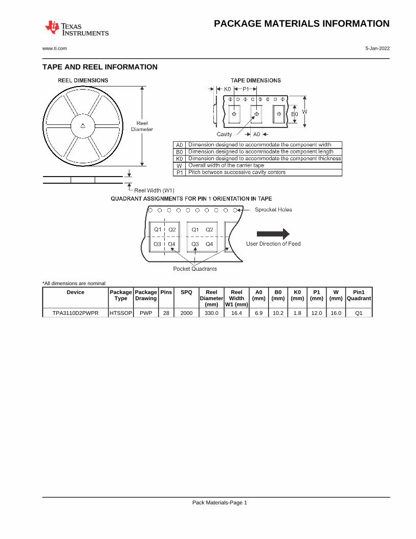
TAPE AND REEL INFORMATION
*All dimensions are nominal
Device PackageType
PackageDrawing
Pins SPQ ReelDiameter
(mm)
ReelWidth
W1 (mm)
A0(mm)
B0(mm)
K0(mm)
P1(mm)
W(mm)
Pin1Quadrant
TPA3110D2PWPR HTSSOP PWP 28 2000 330.0 16.4 6.9 10.2 1.8 12.0 16.0 Q1
PACKAGE MATERIALS INFORMATION
www.ti.com 5-Jan-2022
Pack Materials-Page 1

*All dimensions are nominal
Device Package Type Package Drawing Pins SPQ Length (mm) Width (mm) Height (mm)
TPA3110D2PWPR HTSSOP PWP 28 2000 350.0 350.0 43.0
PACKAGE MATERIALS INFORMATION
www.ti.com 5-Jan-2022
Pack Materials-Page 2

TUBE
*All dimensions are nominal
Device Package Name Package Type Pins SPQ L (mm) W (mm) T (µm) B (mm)
TPA3110D2PWP PWP HTSSOP 28 50 530 10.2 3600 3.5
PACKAGE MATERIALS INFORMATION
www.ti.com 5-Jan-2022
Pack Materials-Page 3

www.ti.com
GENERIC PACKAGE VIEW
This image is a representation of the package family, actual package may vary.Refer to the product data sheet for package details.
TSSOP - 1.2 mm max heightTMPowerPADPWP 28SMALL OUTLINE PACKAGE4.4 x 9.7, 0.65 mm pitch
4224765/B

IMPORTANT NOTICE AND DISCLAIMERTI PROVIDES TECHNICAL AND RELIABILITY DATA (INCLUDING DATA SHEETS), DESIGN RESOURCES (INCLUDING REFERENCE DESIGNS), APPLICATION OR OTHER DESIGN ADVICE, WEB TOOLS, SAFETY INFORMATION, AND OTHER RESOURCES “AS IS” AND WITH ALL FAULTS, AND DISCLAIMS ALL WARRANTIES, EXPRESS AND IMPLIED, INCLUDING WITHOUT LIMITATION ANY IMPLIED WARRANTIES OF MERCHANTABILITY, FITNESS FOR A PARTICULAR PURPOSE OR NON-INFRINGEMENT OF THIRD PARTY INTELLECTUAL PROPERTY RIGHTS.These resources are intended for skilled developers designing with TI products. You are solely responsible for (1) selecting the appropriate TI products for your application, (2) designing, validating and testing your application, and (3) ensuring your application meets applicable standards, and any other safety, security, regulatory or other requirements.These resources are subject to change without notice. TI grants you permission to use these resources only for development of an application that uses the TI products described in the resource. Other reproduction and display of these resources is prohibited. No license is granted to any other TI intellectual property right or to any third party intellectual property right. TI disclaims responsibility for, and you will fully indemnify TI and its representatives against, any claims, damages, costs, losses, and liabilities arising out of your use of these resources.TI’s products are provided subject to TI’s Terms of Sale or other applicable terms available either on ti.com or provided in conjunction with such TI products. TI’s provision of these resources does not expand or otherwise alter TI’s applicable warranties or warranty disclaimers for TI products.TI objects to and rejects any additional or different terms you may have proposed. IMPORTANT NOTICE
Mailing Address: Texas Instruments, Post Office Box 655303, Dallas, Texas 75265Copyright © 2022, Texas Instruments Incorporated
Recommended