TMS320F28335, TMS320F28334, TMS320F28332Digital Signal Controllers (DSCs)
Data Manual
Literature Number: SPRS439
June 2007
PRODUCT PREVIEW information concerns products in theformative or design phase of development. Characteristic data andother specifications are design goals. Texas Instruments reservesthe right to change or discontinue these products without notice.
http://www.tms320.cn 提供DSP芯片解密,DSP破解等服务 010-62245566 13810019655

www.ti.com
Contents
TMS320F28335, TMS320F28334, TMS320F28332
Digital Signal Controllers (DSCs)SPRS439–JUNE 2007
1 TMS320F28335, TMS320F28334, TMS320F28332 DSCs ............................................................. 71.1 Features....................................................................................................................... 71.2 Getting Started ............................................................................................................... 8
2 Introduction......................................................................................................................... 92.1 Pin Assignments ............................................................................................................. 92.2 Signal Descriptions......................................................................................................... 15
3 Functional Overview ........................................................................................................... 243.1 Memory Maps .............................................................................................................. 253.2 Brief Descriptions........................................................................................................... 32
3.2.1 C28x CPU ....................................................................................................... 323.2.2 Memory Bus (Harvard Bus Architecture) .................................................................... 323.2.3 Peripheral Bus .................................................................................................. 323.2.4 Real-Time JTAG and Analysis ................................................................................ 323.2.5 External Interface (XINTF) ..................................................................................... 333.2.6 Flash .............................................................................................................. 333.2.7 M0, M1 SARAMs ............................................................................................... 333.2.8 L0, L1, L2, L3, L4, L5, L6, L7 SARAMs ..................................................................... 333.2.9 Boot ROM ........................................................................................................ 333.2.10 Security .......................................................................................................... 353.2.11 Peripheral Interrupt Expansion (PIE) Block .................................................................. 353.2.12 External Interrupts (XINT1-XINT7, XNMI).................................................................... 363.2.13 Oscillator and PLL .............................................................................................. 363.2.14 Watchdog ........................................................................................................ 363.2.15 Peripheral Clocking ............................................................................................. 363.2.16 Low-Power Modes .............................................................................................. 363.2.17 Peripheral Frames 0, 1, 2, 3 (PFn) ........................................................................... 373.2.18 General-Purpose Input/Output (GPIO) Multiplexer ......................................................... 373.2.19 32-Bit CPU-Timers (0, 1, 2) ................................................................................... 373.2.20 Control Peripherals ............................................................................................. 383.2.21 Serial Port Peripherals ......................................................................................... 38
3.3 Register Map................................................................................................................ 393.4 Device Emulation Registers............................................................................................... 403.5 Interrupts .................................................................................................................... 41
3.5.1 External Interrupts .............................................................................................. 453.6 System Control ............................................................................................................. 45
3.6.1 OSC and PLL Block ............................................................................................ 473.6.2 Watchdog Block ................................................................................................. 50
3.7 Low-Power Modes Block .................................................................................................. 51
4 Peripherals ........................................................................................................................ 524.1 DMA Overview.............................................................................................................. 534.2 32-Bit CPU-Timers 0/1/2 .................................................................................................. 544.3 Enhanced PWM Modules (ePWM1/2/3/4/5/6).......................................................................... 564.4 High-Resolution PWM (HRPWM) ........................................................................................ 584.5 Enhanced CAP Modules (eCAP1/2/3/4/5/6) ............................................................................ 594.6 Enhanced QEP Modules (eQEP1/2)..................................................................................... 614.7 Enhanced Analog-to-Digital Converter (ADC) Module ................................................................ 63
4.7.1 ADC Connections if the ADC Is Not Used ................................................................... 664.7.2 ADC Registers ................................................................................................... 66
4.8 Multichannel Buffered Serial Port (McBSP) Module ................................................................... 684.9 Enhanced Controller Area Network (eCAN) Modules (eCAN-A and eCAN-B)..................................... 71
Contents2 Submit Documentation Feedback
http://www.tms320.cn 提供DSP芯片解密,DSP破解等服务 010-62245566 13810019655
www.ti.com
TMS320F28335, TMS320F28334, TMS320F28332
Digital Signal Controllers (DSCs)SPRS439–JUNE 2007
4.10 Serial Communications Interface (SCI) Modules (SCI-A, SCI-B, SCI-C) ........................................... 764.11 Serial Peripheral Interface (SPI) Module (SPI-A) ...................................................................... 804.12 Inter-Integrated Circuit (I2C) .............................................................................................. 834.13 GPIO MUX .................................................................................................................. 85
5 Device Support .................................................................................................................. 915.1 Device and Development Support Tool Nomenclature................................................................ 915.2 Documentation Support ................................................................................................... 93
6 Electrical Specifications ...................................................................................................... 966.1 Absolute Maximum Ratings ............................................................................................... 966.2 Recommended Operating Conditions ................................................................................... 976.3 Electrical Characteristics ................................................................................................. 97
Contents 3
http://www.tms320.cn 提供DSP芯片解密,DSP破解等服务 010-62245566 13810019655
www.ti.com
TMS320F28335, TMS320F28334, TMS320F28332
Digital Signal Controllers (DSCs)SPRS439–JUNE 2007
List of Figures2-1 F28335, F28334, F28332 176-Pin PGF LQFP (Top View).................................................................. 10
2-2 F28335, F28334, F28332 179-Ball ZHH MicroStar BGA™ (Upper Left Quadrant) (Bottom View) .................... 11
2-3 F28335, F28334, F28332 179-Ball ZHH MicroStar BGA™ (Upper Right Quadrant) (Bottom View) .................. 12
2-4 F28335, F28334, F28332 179-Ball ZHH MicroStar BGA™ (Lower Left Quadrant) (Bottom View) .................... 13
2-5 F28335, F28334, F28332 179-Ball ZHH MicroStar BGA™ (Lower Right Quadrant) (Bottom View) .................. 14
3-1 Functional Block Diagram ....................................................................................................... 24
3-2 F28335 Memory Map ............................................................................................................. 26
3-3 F28334 Memory Map ............................................................................................................. 27
3-4 F28332 Memory Map ............................................................................................................. 28
3-5 External and PIE Interrupt Sources............................................................................................. 41
3-6 External Interrupts ................................................................................................................ 42
3-7 Multiplexing of Interrupts Using the PIE Block ................................................................................ 43
3-8 Clock and Reset Domains ....................................................................................................... 46
3-9 OSC and PLL Block Diagram ................................................................................................... 47
3-10 Using a 3.3-V External Oscillator ............................................................................................... 48
3-11 Using a 1.8-V External Oscillator ............................................................................................... 48
3-12 Using the Internal Oscillator ..................................................................................................... 48
3-13 Watchdog Module................................................................................................................. 50
4-1 DMA Functional Block Diagram ................................................................................................. 53
4-2 CPU-Timers........................................................................................................................ 54
4-3 CPU-Timer Interrupt Signals and Output Signal .............................................................................. 54
4-4 Multiple PWM Modules in a 2833x System.................................................................................... 56
4-5 ePWM Sub-Modules Showing Critical Internal Signal Interconnections ................................................... 58
4-6 eCAP Functional Block Diagram ................................................................................................ 59
4-7 eQEP Functional Block Diagram................................................................................................ 61
4-8 Block Diagram of the ADC Module ............................................................................................. 64
4-9 ADC Pin Connections With Internal Reference ............................................................................... 65
4-10 ADC Pin Connections With External Reference .............................................................................. 65
4-11 McBSP Module ................................................................................................................... 69
4-12 eCAN Block Diagram and Interface Circuit .................................................................................... 72
4-13 eCAN-A Memory Map ............................................................................................................ 73
4-14 eCAN-B Memory Map ............................................................................................................ 74
4-15 Serial Communications Interface (SCI) Module Block Diagram ............................................................ 79
4-16 SPI Module Block Diagram (Slave Mode) ..................................................................................... 82
4-17 I2C Peripheral Module Interfaces ............................................................................................... 84
4-18 GPIO MUX Block Diagram....................................................................................................... 85
4-19 Qualification Using Sampling Window.......................................................................................... 90
5-1 Example of 2833x Device Nomenclature ...................................................................................... 92
List of Figures4 Submit Documentation Feedback
http://www.tms320.cn 提供DSP芯片解密,DSP破解等服务 010-62245566 13810019655

www.ti.com
TMS320F28335, TMS320F28334, TMS320F28332
Digital Signal Controllers (DSCs)SPRS439–JUNE 2007
List of Tables2-1 Hardware Features ................................................................................................................ 9
2-2 Signal Descriptions ............................................................................................................... 15
3-1 Addresses of Flash Sectors in F28335......................................................................................... 29
3-2 Addresses of Flash Sectors in F28334......................................................................................... 29
3-3 Addresses of Flash Sectors in F28332......................................................................................... 29
3-4 Handling Security Code Locations.............................................................................................. 30
3-5 Wait-states ......................................................................................................................... 31
3-6 Boot Mode Selection.............................................................................................................. 34
3-7 Peripheral Frame 0 Registers ................................................................................................... 39
3-8 Peripheral Frame 1 Registers ................................................................................................... 39
3-9 Peripheral Frame 2 Registers ................................................................................................... 40
3-10 Peripheral Frame 3 Registers ................................................................................................... 40
3-11 Device Emulation Registers ..................................................................................................... 40
3-12 PIE Peripheral Interrupts ......................................................................................................... 43
3-13 PIE Configuration and Control Registers ...................................................................................... 44
3-14 External Interrupt Registers...................................................................................................... 45
3-15 PLL, Clocking, Watchdog, and Low-Power Mode Registers ................................................................ 47
3-16 PLLCR Register Bit Definitions.................................................................................................. 49
3-17 CLKIN Divide Options ............................................................................................................ 49
3-18 Possible PLL Configuration Modes ............................................................................................. 49
3-19 Low-Power Modes ................................................................................................................ 51
4-1 CPU-Timers 0, 1, 2 Configuration and Control Registers ................................................................... 55
4-2 ePWM Control and Status Registers ........................................................................................... 57
4-3 eCAP Control and Status Registers ............................................................................................ 60
4-4 eQEP Control and Status Registers ............................................................................................ 62
4-5 ADC Registers..................................................................................................................... 66
4-6 McBSP Register Summary ...................................................................................................... 70
4-7 3.3-V eCAN Transceivers ....................................................................................................... 72
4-8 CAN Register Map ................................................................................................................ 75
4-9 SCI-A Registers ................................................................................................................... 77
4-10 SCI-B Registers ................................................................................................................... 77
4-11 SCI-C Registers ................................................................................................................... 78
4-12 SPI-A Registers ................................................................................................................... 81
4-13 I2C-A Registers.................................................................................................................... 84
4-14 GPIO Registers ................................................................................................................... 86
4-15 GPIO-A Mux Peripheral Selection Matrix ..................................................................................... 87
4-16 GPIO-B Mux Peripheral Selection Matrix ..................................................................................... 88
4-17 GPIO-C Mux Peripheral Selection Matrix ..................................................................................... 89
List of Tables 5
http://www.tms320.cn 提供DSP芯片解密,DSP破解等服务 010-62245566 13810019655

www.ti.com
TMS320F28335, TMS320F28334, TMS320F28332
Digital Signal Controllers (DSCs)SPRS439–JUNE 2007
List of Tables6 Submit Documentation Feedback
http://www.tms320.cn 提供DSP芯片解密,DSP破解等服务 010-62245566 13810019655
www.ti.com
PR
OD
UC
T P
RE
VIE
W
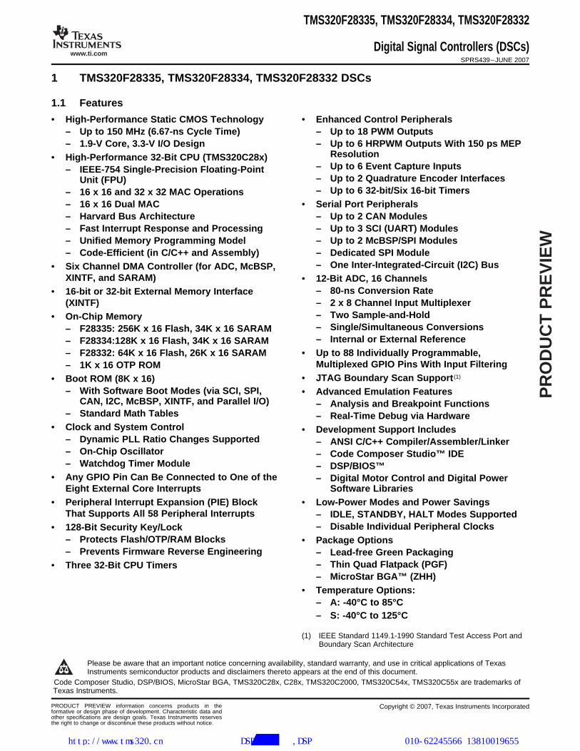
1 TMS320F28335, TMS320F28334, TMS320F28332 DSCs
1.1 Features
TMS320F28335, TMS320F28334, TMS320F28332
Digital Signal Controllers (DSCs)SPRS439–JUNE 2007
• High-Performance Static CMOS Technology • Enhanced Control Peripherals– Up to 150 MHz (6.67-ns Cycle Time) – Up to 18 PWM Outputs– 1.9-V Core, 3.3-V I/O Design – Up to 6 HRPWM Outputs With 150 ps MEP
Resolution• High-Performance 32-Bit CPU (TMS320C28x)– Up to 6 Event Capture Inputs– IEEE-754 Single-Precision Floating-Point– Up to 2 Quadrature Encoder InterfacesUnit (FPU)– Up to 6 32-bit/Six 16-bit Timers– 16 x 16 and 32 x 32 MAC Operations
– 16 x 16 Dual MAC • Serial Port Peripherals– Harvard Bus Architecture – Up to 2 CAN Modules– Fast Interrupt Response and Processing – Up to 3 SCI (UART) Modules– Unified Memory Programming Model – Up to 2 McBSP/SPI Modules– Code-Efficient (in C/C++ and Assembly) – Dedicated SPI Module
– One Inter-Integrated-Circuit (I2C) Bus• Six Channel DMA Controller (for ADC, McBSP,XINTF, and SARAM) • 12-Bit ADC, 16 Channels
– 80-ns Conversion Rate• 16-bit or 32-bit External Memory Interface(XINTF) – 2 x 8 Channel Input Multiplexer
– Two Sample-and-Hold• On-Chip Memory– Single/Simultaneous Conversions– F28335: 256K x 16 Flash, 34K x 16 SARAM– Internal or External Reference– F28334:128K x 16 Flash, 34K x 16 SARAM
– F28332: 64K x 16 Flash, 26K x 16 SARAM • Up to 88 Individually Programmable,Multiplexed GPIO Pins With Input Filtering– 1K x 16 OTP ROM
• JTAG Boundary Scan Support (1)• Boot ROM (8K x 16)– With Software Boot Modes (via SCI, SPI, • Advanced Emulation Features
CAN, I2C, McBSP, XINTF, and Parallel I/O) – Analysis and Breakpoint Functions– Standard Math Tables – Real-Time Debug via Hardware
• Clock and System Control • Development Support Includes– Dynamic PLL Ratio Changes Supported – ANSI C/C++ Compiler/Assembler/Linker– On-Chip Oscillator – Code Composer Studio™ IDE– Watchdog Timer Module – DSP/BIOS™
• Any GPIO Pin Can Be Connected to One of the – Digital Motor Control and Digital PowerEight External Core Interrupts Software Libraries
• Peripheral Interrupt Expansion (PIE) Block • Low-Power Modes and Power SavingsThat Supports All 58 Peripheral Interrupts – IDLE, STANDBY, HALT Modes Supported
– Disable Individual Peripheral Clocks• 128-Bit Security Key/Lock– Protects Flash/OTP/RAM Blocks • Package Options– Prevents Firmware Reverse Engineering – Lead-free Green Packaging
– Thin Quad Flatpack (PGF)• Three 32-Bit CPU Timers– MicroStar BGA™ (ZHH)
• Temperature Options:– A: -40°C to 85°C– S: -40°C to 125°C
(1) IEEE Standard 1149.1-1990 Standard Test Access Port andBoundary Scan Architecture
Please be aware that an important notice concerning availability, standard warranty, and use in critical applications of TexasInstruments semiconductor products and disclaimers thereto appears at the end of this document.
Code Composer Studio, DSP/BIOS, MicroStar BGA, TMS320C28x, C28x, TMS320C2000, TMS320C54x, TMS320C55x are trademarks ofTexas Instruments.
PRODUCT PREVIEW information concerns products in the Copyright © 2007, Texas Instruments Incorporatedformative or design phase of development. Characteristic data andother specifications are design goals. Texas Instruments reservesthe right to change or discontinue these products without notice.
http://www.tms320.cn 提供DSP芯片解密,DSP破解等服务 010-62245566 13810019655

www.ti.com
PR
OD
UC
T P
RE
VIE
W
1.2 Getting Started
TMS320F28335, TMS320F28334, TMS320F28332
Digital Signal Controllers (DSCs)SPRS439–JUNE 2007
This section gives a brief overview of the steps to take when first developing for a C28x device. For moredetail on each of these steps, see the following:• Getting Started With TMS320C28x™ Digital Signal Controllers (literature number SPRAAM0).• C2000 Getting Started Website (http://www.ti.com/c2000getstarted)
8 TMS320F28335, TMS320F28334, TMS320F28332 DSCs Submit Documentation Feedback
http://www.tms320.cn 提供DSP芯片解密,DSP破解等服务 010-62245566 13810019655
www.ti.com
PR
OD
UC
T P
RE
VIE
W
2 Introduction
2.1 Pin Assignments
TMS320F28335, TMS320F28334, TMS320F28332
Digital Signal Controllers (DSCs)SPRS439–JUNE 2007
The TMS320F28335, TMS320F28334, and TMS320F28332, devices, members of the TMS320C28x™DSC generation, are highly integrated, high-performance solutions for demanding control applications.
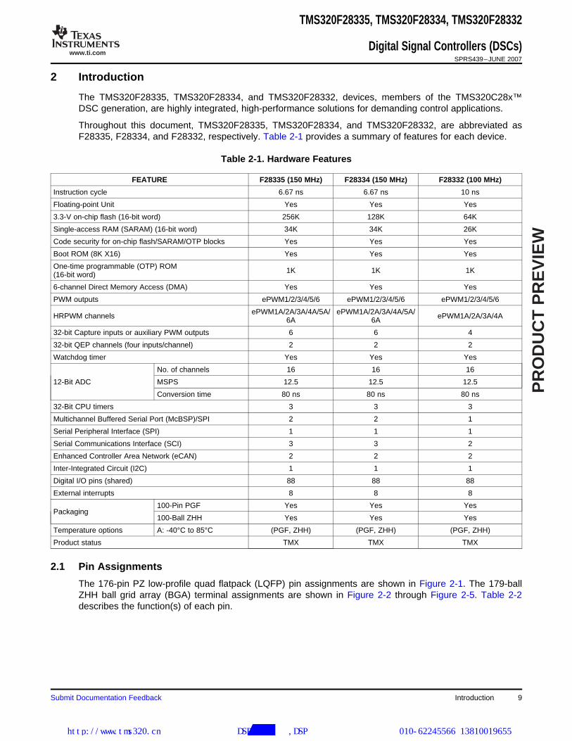
Throughout this document, TMS320F28335, TMS320F28334, and TMS320F28332, are abbreviated asF28335, F28334, and F28332, respectively. Table 2-1 provides a summary of features for each device.
Table 2-1. Hardware Features
FEATURE F28335 (150 MHz) F28334 (150 MHz) F28332 (100 MHz)
Instruction cycle 6.67 ns 6.67 ns 10 ns
Floating-point Unit Yes Yes Yes
3.3-V on-chip flash (16-bit word) 256K 128K 64K
Single-access RAM (SARAM) (16-bit word) 34K 34K 26K
Code security for on-chip flash/SARAM/OTP blocks Yes Yes Yes
Boot ROM (8K X16) Yes Yes Yes
One-time programmable (OTP) ROM 1K 1K 1K(16-bit word)
6-channel Direct Memory Access (DMA) Yes Yes Yes
PWM outputs ePWM1/2/3/4/5/6 ePWM1/2/3/4/5/6 ePWM1/2/3/4/5/6
ePWM1A/2A/3A/4A/5A/ ePWM1A/2A/3A/4A/5A/HRPWM channels ePWM1A/2A/3A/4A6A 6A
32-bit Capture inputs or auxiliary PWM outputs 6 6 4
32-bit QEP channels (four inputs/channel) 2 2 2
Watchdog timer Yes Yes Yes
No. of channels 16 16 16
12-Bit ADC MSPS 12.5 12.5 12.5
Conversion time 80 ns 80 ns 80 ns
32-Bit CPU timers 3 3 3
Multichannel Buffered Serial Port (McBSP)/SPI 2 2 1
Serial Peripheral Interface (SPI) 1 1 1
Serial Communications Interface (SCI) 3 3 2
Enhanced Controller Area Network (eCAN) 2 2 2
Inter-Integrated Circuit (I2C) 1 1 1
Digital I/O pins (shared) 88 88 88
External interrupts 8 8 8
100-Pin PGF Yes Yes YesPackaging
100-Ball ZHH Yes Yes Yes
Temperature options A: -40°C to 85°C (PGF, ZHH) (PGF, ZHH) (PGF, ZHH)
Product status TMX TMX TMX
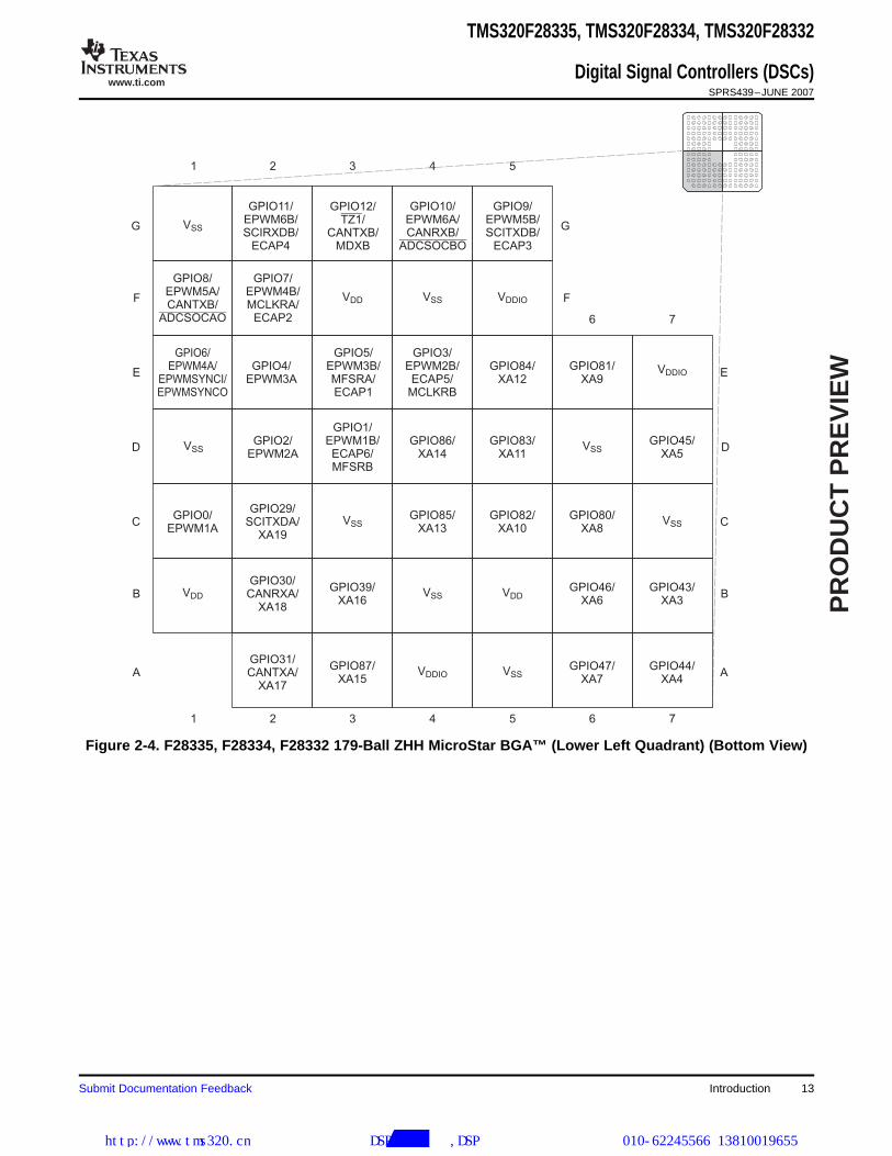
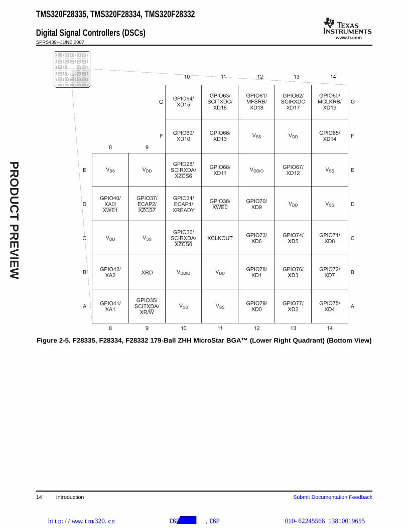
The 176-pin PZ low-profile quad flatpack (LQFP) pin assignments are shown in Figure 2-1. The 179-ballZHH ball grid array (BGA) terminal assignments are shown in Figure 2-2 through Figure 2-5. Table 2-2describes the function(s) of each pin.
Submit Documentation Feedback Introduction 9
http://www.tms320.cn 提供DSP芯片解密,DSP破解等服务 010-62245566 13810019655

www.ti.com
PR
OD
UC
T P
RE
VIE
W
88
87
86
85
84
83
82
81
80
79
78
77
76
75
74
73
72
71
70
69
68
67
66
65
64
63
62
61
60
59
58
57
56
55
54
53
52
51
50
49
48
47
46
45
133
134
135
136
137
138
139
140
141
142
143
144
145
146
147
148
149
150
151
152
153
154
155
156
157
158
159
160
161
162
163
164
165
166
167
168
169
170
171
172
173
174
175
176
1 2 3 4 5 6 7 8 9 10
11
12
13
14
15
16
17
18
19
20
21
22
23
24
25
26
27
28
29
30
31
32
33
34
35
36
37
38
39
40
41
42
43
44
13
2
13
1
13
0
12
9
12
8
12
7
12
6
12
5
12
4
12
3
12
2
12
1
12
0
11
9
11
8
11
7
11
6
11
5
11
4
11
3
11
2
111
11
0
10
9
10
8
10
7
10
6
10
5
10
4
10
3
10
2
10
1
10
0
99
98
97
96
95
94
93
92
91
90
89
GPIO48/ECAP5/XD31
TCK
EMU1
EMU0VDD3VFLVSS
TEST2
TEST1
XRS
TMS
TRST
TDO
TDI
GPIO33/SCLA/EPWMSYNCO/ADCSOCBO
GPIO32/SDAA/EPWMSYNCI/ADCSOCAO
GPIO27/ECAP4/EQEP2S/MFSXB
GPIO26/ECAP3/EQEP2I/MCLKXBVDDIOVSS
GPIO25/ECAP2/EQEP2B/MDRB
GPIO24/ECAP1/EQEP2A/MDXB
GPIO23/EQEP1I/MFSXA/SCIRXDB
GPIO22/EQEP1S/MCLKXA/SCITXDB
GPIO21/EQEP1B/MDRA/CANRXB
GPIO20/EQEP1A/MDXA/CANTXB
GPIO19/ /SCIRXDB/CANTXASPISTEA
GPIO18/SPICLKA/SCITXDB/CANRXAVDDVSSVDD2A18
VSS2AGND
ADCRESEXT
ADCREFP
ADCREFM
ADCREFIN
ADCINB7ADCINB6
ADCINB5
ADCINB4
ADCINB3
ADCINB2
ADCINB1
ADCINB0
VDDAIO
GP
IO7
5/X
D4
GP
IO7
4/X
D5
GP
IO7
3/X
D6
GP
IO7
2/X
D7
GP
IO7
1/X
D8
GP
IO7
0/X
D9
VD
DV
SS
GP
IO6
9/X
D1
0
GP
IO6
8/X
D11
GP
IO6
7/X
D1
2
VD
DIO
VS
SG
PIO
66
/XD
13
VS
SV
DD
GP
IO6
5/X
D1
4G
PIO
64
/XD
15
GP
IO6
3/S
CIT
XD
C/X
D1
6
GP
IO6
2/S
CIR
XD
C/X
D1
7
GP
IO6
1/M
FS
RB
/XD
18
GP
IO6
0/M
CL
KR
B/X
D1
9
GP
IO5
9/M
FS
RA
/XD
20
VD
DV
SS
VD
DIO
VS
S
XC
LK
INX
1
VS
S
X2
VD
DG
PIO
58
/MC
LK
RA
/XD
21
GP
IO5
7/
/XD
22
SP
IST
EA
GP
IO5
6/S
PIC
LK
A/X
D2
3
GP
IO5
5/S
PIS
OM
IA/X
D2
4G
PIO
54
/SP
ISIM
OA
/XD
25
GP
IO5
3/E
QE
P1
I/X
D2
6
GP
IO5
2/E
QE
P1
S/X
D2
7
VD
DIO
VS
SG
PIO
51
/EQ
EP
1B
/XD
28
GP
IO5
0/E
QE
P1
A/X
D2
9
GP
IO4
9/E
CA
P6
/XD
30
GP
IO3
0/C
AN
RX
A/X
A1
8
GP
IO2
9/S
CIT
XD
A/X
A1
9
VS
SV
DD
GP
IO0
/EP
WM
1A
GP
IO1
/EP
WM
1B
/EC
AP
6/M
FS
RB
GP
IO2
/EP
WM
2A
VS
SV
DD
IO
GP
IO3
/EP
WM
2B
/EC
AP
5/M
CL
KR
B
GP
IO4
/EP
WM
3A
GP
IO5
/EP
WM
3B
/MF
SR
A/E
CA
P1
GP
IO6
/EP
WM
4A
/EP
WM
SY
NC
I/E
PW
MS
YN
CO
VS
SV
DD
GP
IO7
/EP
WM
4B
/MC
LK
RA
/EC
AP
2
GP
IO8
/EP
WM
5A
/CA
NT
XB
/ AD
CS
OC
AO
GP
IO9
/EP
WM
5B
/SC
ITX
DB
/EC
AP
3
GP
IO1
0/E
PW
M6
A/C
AN
RX
B/ A
DC
SO
CB
O
GP
IO11
/EP
WM
6B
/SC
IRX
DB
/EC
AP
4
GP
IO1
2/C
AN
TX
B/M
DX
B/T
Z1
VS
SV
DD
GP
IO1
3/
/CA
NR
XB
/MD
RB
TZ
2
GP
IO1
4/
/XH
OL
D/
/T
Z3
SC
ITX
DB
MC
LK
XB
GP
IO1
5/
/XH
OL
DA
TZ
4/S
CIR
XD
B/M
FS
XB
GP
IO1
6/S
PIS
IMO
A/C
AN
TX
B/T
Z5
GP
IO1
7/S
PIS
OM
IA/C
AN
RX
B/T
Z6
VD
DV
SS
VD
D1A
18
VS
S1
AG
ND
VS
SA
2V
DD
A2
AD
CIN
A7
AD
CIN
A6
AD
CIN
A5
AD
CIN
A4
AD
CIN
A3
AD
CIN
A2
AD
CIN
A1
AD
CIN
A0
AD
CL
O
VS
SA
IO
GPIO76/XD3
GPIO77/XD2
GPIO78/XD1
GPIO79/XD0
GPIO38/XWE0XCLKOUT
VDDVSS
GPIO28/SCIRXDA/XZCS6
GPIO34/ECAP1/XREADY
VDDIOVSS
GPIO36/SCIRXDA/XZCS0VDDVSS
GPIO35/SCITXDA/XR/W
XRDGPIO37/ECAP2/XZCS7
GPIO40/XA0/XWE1
GPIO41/XA1
GPIO42/XA2VDDVSS
GPIO43/XA3
GPIO44/XA4
GPIO45/XA5VDDIO
VSSGPIO46/XA6
GPIO47/XA7
GPIO80/XA8
GPIO81/XA9
GPIO82/XA10
VSSVDD
GPIO83/XA11
GPIO84/XA12VDDIO
VSSGPIO85/XA13
GPIO86/XA14
GPIO87/XA15
GPIO39/XA16
GPIO31/CANTXA/XA17
GPIO28/SCIRXDA/XZCS6
TMS320F28335, TMS320F28334, TMS320F28332
Digital Signal Controllers (DSCs)SPRS439–JUNE 2007
Figure 2-1. F28335, F28334, F28332 176-Pin PGF LQFP (Top View)
Introduction10 Submit Documentation Feedback
http://www.tms320.cn 提供DSP芯片解密,DSP破解等服务 010-62245566 13810019655

www.ti.com
PR
OD
UC
T P
RE
VIE
W
ADCINB0 ADCINB2 ADCINB6 ADCREFP
ADCINA1
ADCRESEXTADCINA2 ADCLO ADCINA0 ADCINB4
VSS1AGND
ADCINA4 ADCINA3 ADCINB3 ADCREFIN
P P
N N
M M
L LADCINA5
GPIO18/
SPICLKA/
SCITXDB/
CANRXA
VSSA2 ADCINA7 ADCINB7
GPIO17/
SPISOMIA/
CANRXB/
TZ6
VDD1A18VDD
GPIO14/
/
SCITXDB/
MCLKXB
TZ3 XHOLD/
GPIO13/
CANRXB/
MDRB
TZ2/
VDDAIO
K K
J J
H H
1 2 3 4 5
6 7
GPIO20/
EQEP1A/
MDXA/
CANTXB
VSS2AGND
GPIO21/
EQEP1B/
MDRA/
CANRXB
GPIO22/
EQEP1S/
MCLKXA/
SCITXDB
VSS
1 2 3 4 5 6 7
VSSAIO VSS
VDD
VDD
GPIO23/
EQEP1I/
MFSXA/
SCIRXDB
GPIO19/
SCIRXDB/
CANTXA
SPISTEA/
ADCINA6
GPIO16/
SPISIMOA/
CANTXB/
TZ5
GPIO15/
/
SCIRXDB/
MFSXB
TZ4 XHOLDA/
VDDA2
VDD2A18
ADCREFMADCINB5ADCINB1
TMS320F28335, TMS320F28334, TMS320F28332
Digital Signal Controllers (DSCs)SPRS439–JUNE 2007
Figure 2-2. F28335, F28334, F28332 179-Ball ZHH MicroStar BGA™ (Upper Left Quadrant) (Bottom View)
Submit Documentation Feedback Introduction 11
http://www.tms320.cn 提供DSP芯片解密,DSP破解等服务 010-62245566 13810019655

www.ti.com
PR
OD
UC
T P
RE
VIE
W
GPIO50/
EQEP1A/
XD29
TMS TEST2 EMU1
GPIO51/
EQEP1B/
XD28
GPIO48/
ECAP5/
XD31
TCK
GPIO52/
EQEP1S/
XD27
VSS
GPIO27/
ECAP4/
EQEP2S/
MFSXB
XRS EMU0
GPIO53/
EQEP1I/
XD26
VDD
GPIO55/
SPISOMIA/
XD24
VSS
GPIO56/
SPICLKA/
XD23
GPIO58/
MCLKRA/
XD21
GPIO33/
SCLA/
EPWMSYNCO/
ADCSOCBO
TRST
GPIO32/
SDAA/
EPWMSYNCI/
ADCSOCAO
VDDIO
8 9
10 11 12 13 14
PP
NN
MM
LL
KK
JJ
HH
GPIO57/
/
XD22
SPISTEA
X1 XCLKIN
GPIO59/
MFSRA/
XD20
VSS
GPIO25/
ECAP2/
EQEP2B/
MDRB
VSS
VDD
VSS
8 9 10 11 12 13 14
VSS
VSS
TEST1
VDD3VFL
GPIO24/
ECAP1/
EQEP2A/
MDXB
GPIO26/
ECAP3/
EQEP2I/
MCLKXB
TDO
VDDIO
VSSX2
GPIO54/
SPISIMOA/
XD25
TDI
VDDIO
GPIO49/
ECAP6/
XD30
TMS320F28335, TMS320F28334, TMS320F28332
Digital Signal Controllers (DSCs)SPRS439–JUNE 2007
Figure 2-3. F28335, F28334, F28332 179-Ball ZHH MicroStar BGA™ (Upper Right Quadrant) (Bottom View)
Introduction12 Submit Documentation Feedback
http://www.tms320.cn 提供DSP芯片解密,DSP破解等服务 010-62245566 13810019655
www.ti.com
PR
OD
UC
T P
RE
VIE
W
GPIO11
EPWM6B
SCIRXDB
ECAP4
/
/
/
GPIO12
CANTXB
MDXB
TZ1
/
/
/
GPIO10
EPWM6A
CANRXB
ADCSOCBO
/
/
/
GPIO9/
EPWM5B/
SCITXDB/
ECAP3
GPIO81/
XA9
GPIO8/
EPWM5A/
CANTXB/
ADCSOCAO
GPIO7/
EPWM4B/
MCLKRA/
ECAP2
GPIO84/
XA12
GPIO6/
EPWM4A/
EPWMSYNCI/
EPWMSYNCO
GPIO4/
EPWM3A
GPIO5/
EPWM3B/
MFSRA/
ECAP1
GPIO3/
EPWM2B/
ECAP5/
MCLKRB
VDDIO
VDDIO
VSSGPIO2/
EPWM2A
GPIO1/
EPWM1B/
ECAP6/
MFSRB
GPIO86/
XA14
GPIO83/
XA11
G
F
E
D
GPIO0/
EPWM1A
GPIO29/
SCITXDA/
XA19
VSSGPIO85/
XA13
GPIO82/
XA10
VDD
GPIO30/
CANRXA/
XA18
GPIO39/
XA16VSS VDD
GPIO31/
CANTXA/
XA17
GPIO87/
XA15VDDIO
C
B
A
1 2 3 4 5 6 7
G
F
E
D
C
B
A
VSSGPIO45/
XA5
VSSGPIO80/
XA8
GPIO46/
XA6
GPIO43/
XA3
GPIO44/
XA4
GPIO47/
XA7VSS
1 2 3 4 5
6 7
VSSVDD
VSS
TMS320F28335, TMS320F28334, TMS320F28332
Digital Signal Controllers (DSCs)SPRS439–JUNE 2007
Figure 2-4. F28335, F28334, F28332 179-Ball ZHH MicroStar BGA™ (Lower Left Quadrant) (Bottom View)
Submit Documentation Feedback Introduction 13
http://www.tms320.cn 提供DSP芯片解密,DSP破解等服务 010-62245566 13810019655
www.ti.com
PR
OD
UC
T P
RE
VIE
W
GPIO60/
MCLKRB/
XD19
GPIO64/
XD15
GPIO63/
SCITXDC/
XD16
GPIO61/
MFSRB/
XD18
GPIO67/
XD12
GPIO65/
XD14
GPIO62/
SCIRXDC
XD17
GPIO78/
XD1
GPIO79/
XD0
GPIO66/
XD13
GPIO68/
XD11
VSS
GPIO37/
ECAP2/
XZCS7
GPIO34/
ECAP1/
XREADY
GPIO38/
XWE0
GPIO70/
XD9
G
F
E
D
VDD
GPIO40/
XA0/
XWE1
VSS
XCLKOUTGPIO73/
XD6
GPIO42/
XA2XRD
GPIO28/
SCIRXDA/
XZCS6
VDD
GPIO35/
SCITXDA/
XR/W
GPIO69/
XD10
VDDIO
C
B
A
8 9 10 11 12 13 14
G
F
E
D
C
B
A
GPIO74/
XD5
GPIO76/
XD3
GPIO72/
XD7
GPIO75/
XD4
GPIO77/
XD2
VSS
GPIO41/
XA1
VSS
VDD
VSS
8 9
10 11 12 13 14
VSS VDD
VSS
VDDIO
GPIO36/
SCIRXDA/
XZCS0
VDD
GPIO71/
XD8
TMS320F28335, TMS320F28334, TMS320F28332
Digital Signal Controllers (DSCs)SPRS439–JUNE 2007
Figure 2-5. F28335, F28334, F28332 179-Ball ZHH MicroStar BGA™ (Lower Right Quadrant) (Bottom View)
14 Introduction Submit Documentation Feedback
http://www.tms320.cn 提供DSP芯片解密,DSP破解等服务 010-62245566 13810019655

www.ti.com
PR
OD
UC
T P
RE
VIE
W
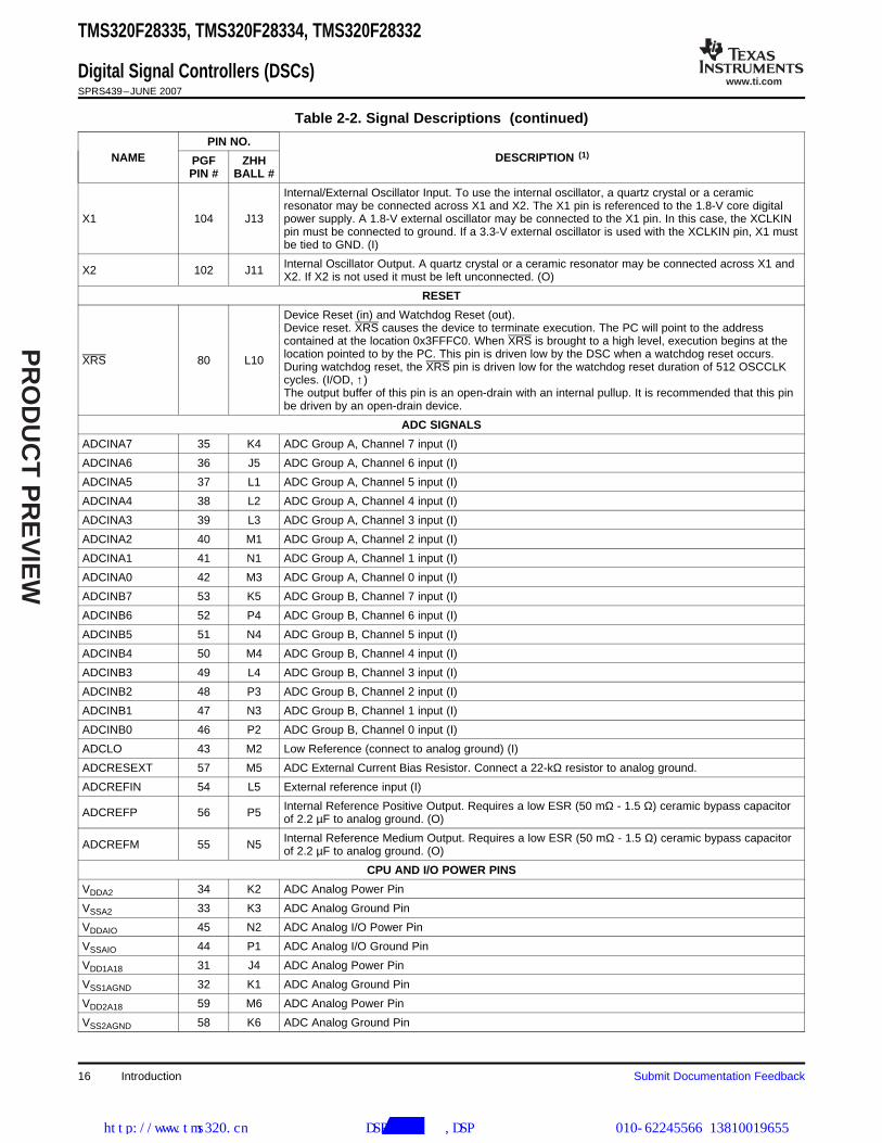
2.2 Signal Descriptions
TMS320F28335, TMS320F28334, TMS320F28332
Digital Signal Controllers (DSCs)SPRS439–JUNE 2007
Table 2-2 describes the signals on the 2833x devices. All digital inputs are TTL-compatible. All outputs are3.3 V with CMOS levels. Inputs are not 5-V tolerant.
Table 2-2. Signal Descriptions
PIN NO.NAME DESCRIPTION (1)PGF ZHH
PIN # BALL #
JTAG
JTAG test reset with internal pulldown. TRST, when driven high, gives the scan system control ofthe operations of the device. If this signal is not connected or driven low, the device operates in itsfunctional mode, and the test reset signals are ignored.NOTE: Do not use pullup resistors on TRST; it has an internal pull-down device. TRST is an activehigh test pin and must be maintained low at all times during normal device operation. In a low-noiseTRST 78 M10 environment, TRST may be left floating. In other instances, an external pulldown resistor is highlyrecommended. The value of this resistor should be based on drive strength of the debugger podsapplicable to the design. A 2.2-kΩ resistor generally offers adequate protection. Since this isapplication-specific, it is recommended that each target board be validated for proper operation ofthe debugger and the application. (I, ↓)
TCK 87 N12 JTAG test clock with internal pullup (I, ↑)
JTAG test-mode select (TMS) with internal pullup. This serial control input is clocked into the TAPTMS 79 P10 controller on the rising edge of TCK. (I, ↑)
JTAG test data input (TDI) with internal pullup. TDI is clocked into the selected register (instructionTDI 76 M9 or data) on a rising edge of TCK. (I, ↑)
JTAG scan out, test data output (TDO). The contents of the selected register (instruction or data)TDO 77 K9 are shifted out of TDO on the falling edge of TCK. (O/Z 8 mA drive)
Emulator pin 0. When TRST is driven high, this pin is used as an interrupt to or from the emulatorsystem and is defined as input/output through the JTAG scan. This pin is also used to put the deviceinto boundary-scan mode. With the EMU0 pin at a logic-high state and the EMU1 pin at a logic-lowstate, a rising edge on the TRST pin would latch the device into boundary-scan mode. (I/O/Z, 8 mA
EMU0 85 L11 drive ↑)NOTE: An external pullup resistor is recommended on this pin. The value of this resistor should bebased on the drive strength of the debugger pods applicable to the design. A 2.2-kΩ to 4.7-kΩresistor is generally adequate. Since this is application-specific, it is recommended that each targetboard be validated for proper operation of the debugger and the application.
Emulator pin 1. When TRST is driven high, this pin is used as an interrupt to or from the emulatorsystem and is defined as input/output through the JTAG scan. This pin is also used to put the deviceinto boundary-scan mode. With the EMU0 pin at a logic-high state and the EMU1 pin at a logic-lowstate, a rising edge on the TRST pin would latch the device into boundary-scan mode. (I/O/Z, 8 mA
EMU1 86 P12 drive ↑)NOTE: An external pullup resistor is recommended on this pin. The value of this resistor should bebased on the drive strength of the debugger pods applicable to the design. A 2.2-kΩ to 4.7-kΩresistor is generally adequate. Since this is application-specific, it is recommended that each targetboard be validated for proper operation of the debugger and the application.
FLASH
VDD3VFL 84 M11 3.3-V Flash Core Power Pin. This pin should be connected to 3.3 V at all times.
TEST1 81 K10 Test Pin. Reserved for TI. Must be left unconnected. (I/O)
TEST2 82 P11 Test Pin. Reserved for TI. Must be left unconnected. (I/O)
CLOCK
Output clock derived from SYSCLKOUT. XCLKOUT is either the same frequency, one-half thefrequency, or one-fourth the frequency of SYSCLKOUT. This is controlled by the bits 1, 0
XCLKOUT 138 C11 (XCLKOUTDIV) in the XCLK register. At reset, XCLKOUT = SYSCLKOUT/4. The XCLKOUT signalcan be turned off by setting XCLKOUTDIV to 3. Unlike other GPIO pins, the XCLKOUT pin is notplaced in high-impedance state during a reset. (O/Z, 8 mA drive).
External Oscillator Input. This pin is to feed a clock from an external 3.3-V oscillator. In this case, theXCLKIN 105 J14 X1 pin must be tied to GND. If a crystal/resonator is used (or if an external 1.8-V oscillator is used to
feed clock to X1 pin), this pin must be tied to GND. (I)
(1) I = Input, O = Output, Z = High impedance, OD = Open drain, ↑ = Pullup, ↓ = Pulldown
Submit Documentation Feedback Introduction 15
http://www.tms320.cn 提供DSP芯片解密,DSP破解等服务 010-62245566 13810019655
www.ti.com
PR
OD
UC
T P
RE
VIE
W
TMS320F28335, TMS320F28334, TMS320F28332
Digital Signal Controllers (DSCs)SPRS439–JUNE 2007
Table 2-2. Signal Descriptions (continued)
PIN NO.NAME DESCRIPTION (1)PGF ZHH
PIN # BALL #
Internal/External Oscillator Input. To use the internal oscillator, a quartz crystal or a ceramicresonator may be connected across X1 and X2. The X1 pin is referenced to the 1.8-V core digital
X1 104 J13 power supply. A 1.8-V external oscillator may be connected to the X1 pin. In this case, the XCLKINpin must be connected to ground. If a 3.3-V external oscillator is used with the XCLKIN pin, X1 mustbe tied to GND. (I)
Internal Oscillator Output. A quartz crystal or a ceramic resonator may be connected across X1 andX2 102 J11 X2. If X2 is not used it must be left unconnected. (O)
RESET
Device Reset (in) and Watchdog Reset (out).Device reset. XRS causes the device to terminate execution. The PC will point to the addresscontained at the location 0x3FFFC0. When XRS is brought to a high level, execution begins at thelocation pointed to by the PC. This pin is driven low by the DSC when a watchdog reset occurs.XRS 80 L10 During watchdog reset, the XRS pin is driven low for the watchdog reset duration of 512 OSCCLKcycles. (I/OD, ↑)The output buffer of this pin is an open-drain with an internal pullup. It is recommended that this pinbe driven by an open-drain device.
ADC SIGNALS
ADCINA7 35 K4 ADC Group A, Channel 7 input (I)
ADCINA6 36 J5 ADC Group A, Channel 6 input (I)
ADCINA5 37 L1 ADC Group A, Channel 5 input (I)
ADCINA4 38 L2 ADC Group A, Channel 4 input (I)
ADCINA3 39 L3 ADC Group A, Channel 3 input (I)
ADCINA2 40 M1 ADC Group A, Channel 2 input (I)
ADCINA1 41 N1 ADC Group A, Channel 1 input (I)
ADCINA0 42 M3 ADC Group A, Channel 0 input (I)
ADCINB7 53 K5 ADC Group B, Channel 7 input (I)
ADCINB6 52 P4 ADC Group B, Channel 6 input (I)
ADCINB5 51 N4 ADC Group B, Channel 5 input (I)
ADCINB4 50 M4 ADC Group B, Channel 4 input (I)
ADCINB3 49 L4 ADC Group B, Channel 3 input (I)
ADCINB2 48 P3 ADC Group B, Channel 2 input (I)
ADCINB1 47 N3 ADC Group B, Channel 1 input (I)
ADCINB0 46 P2 ADC Group B, Channel 0 input (I)
ADCLO 43 M2 Low Reference (connect to analog ground) (I)
ADCRESEXT 57 M5 ADC External Current Bias Resistor. Connect a 22-kΩ resistor to analog ground.
ADCREFIN 54 L5 External reference input (I)
Internal Reference Positive Output. Requires a low ESR (50 mΩ - 1.5 Ω) ceramic bypass capacitorADCREFP 56 P5 of 2.2 µF to analog ground. (O)
Internal Reference Medium Output. Requires a low ESR (50 mΩ - 1.5 Ω) ceramic bypass capacitorADCREFM 55 N5 of 2.2 µF to analog ground. (O)
CPU AND I/O POWER PINS
VDDA2 34 K2 ADC Analog Power Pin
VSSA2 33 K3 ADC Analog Ground Pin
VDDAIO 45 N2 ADC Analog I/O Power Pin
VSSAIO 44 P1 ADC Analog I/O Ground Pin
VDD1A18 31 J4 ADC Analog Power Pin
VSS1AGND 32 K1 ADC Analog Ground Pin
VDD2A18 59 M6 ADC Analog Power Pin
VSS2AGND 58 K6 ADC Analog Ground Pin
Introduction16 Submit Documentation Feedback
http://www.tms320.cn 提供DSP芯片解密,DSP破解等服务 010-62245566 13810019655
www.ti.com
PR
OD
UC
T P
RE
VIE
W
TMS320F28335, TMS320F28334, TMS320F28332
Digital Signal Controllers (DSCs)SPRS439–JUNE 2007
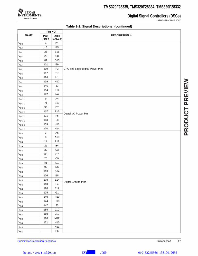
Table 2-2. Signal Descriptions (continued)
PIN NO.NAME DESCRIPTION (1)PGF ZHH
PIN # BALL #
VDD 4 B1
VDD 15 B5
VDD 23 B11
VDD 29 C8
VDD 61 D13
VDD 101 E9
VDD 109 F3 CPU and Logic Digital Power Pins
VDD 117 F13
VDD 126 H1
VDD 139 H12
VDD 146 J2
VDD 154 K14
VDD 167 N6
VDDIO 9 A4
VDDIO 71 B10
VDDIO 93 E7
VDDIO 107 E12Digital I/O Power Pin
VDDIO 121 F5
VDDIO 143 L8
VDDIO 159 H11
VDDIO 170 N14
VSS 3 A5
VSS 8 A10
VSS 14 A11
VSS 22 B4
VSS 30 C3
VSS 60 C7
VSS 70 C9
VSS 83 D1
VSS 92 D6
VSS 103 D14
VSS 106 E8
VSS 108 E14Digital Ground Pins
VSS 118 F4
VSS 120 F12
VSS 125 G1
VSS 140 H10
VSS 144 H13
VSS 147 J3
VSS 155 J10
VSS 160 J12
VSS 166 M12
VSS 171 N10
VSS N11
VSS P6
Submit Documentation Feedback Introduction 17
http://www.tms320.cn 提供DSP芯片解密,DSP破解等服务 010-62245566 13810019655

www.ti.com
PR
OD
UC
T P
RE
VIE
W
TMS320F28335, TMS320F28334, TMS320F28332
Digital Signal Controllers (DSCs)SPRS439–JUNE 2007
Table 2-2. Signal Descriptions (continued)
PIN NO.NAME DESCRIPTION (1)PGF ZHH
PIN # BALL #
VSS P8 Digital Ground Pins
GPIOA AND PERIPHERAL SIGNALS (2) (3)
GPIO0 General purpose input/output 0 (I/O/Z) (4)
EPWM1A Enhanced PWM1 Output A and HRPWM channel (O)5 C1- -- -
GPIO1 General purpose input/output 1 (I/O/Z) (4)
EPWM1B Enhanced PWM1 Output B (O)6 D3ECAP6 Enhanced Capture 6 input/output (I/O)MFSRB McBSP-B receive frame synch (I/O)
GPIO2 General purpose input/output 2 (I/O/Z) (4)
EPWM2A Enhanced PWM2 Output A and HRPWM channel (O)7 D2- -- -
GPIO3 General purpose input/output 3 (I/O/Z) (4)
EPWM2B Enhanced PWM2 Output B (O)10 E4ECAP5 Enhanced Capture 5 input/output (I/O)MCLKRB McBSP-B clock receive (I/O)
GPIO4 General purpose input/output 4 (I/O/Z) (4)
EPWM3A Enhanced PWM3 output A and HRPWM channel (O)11 E2- -- -
GPIO5 General purpose input/output 5 (I/O/Z) (4)
EPWM3B Enhanced PWM3 output B (O)12 E3MFSRA McBSP-A receive frame synch (I/O)ECAP1 Enhanced Capture input/output 1 (I/O)
GPIO6 General purpose input/output 6 (I/O/Z) (4)
EPWM4A Enhanced PWM4 output A and HRPWM channel (O)13 E1EPWMSYNCI External ePWM sync pulse input (I)EPWMSYNCO External ePWM sync pulse output (O)
GPIO7 General purpose input/output 7 (I/O/Z) (4)
EPWM4B Enhanced PWM4 output B (O)16 F2MCLKRA McBSP-A Clock Receive (I/O)ECAP2 Enhanced capture input/output 2 (I/O)
GPIO8 General Purpose Input/Output 8 (I/O/Z) (4)
EPWM5A Enhanced PWM5 output A (O)17 F1CANTXB Enhanced CAN-B transmit (O)ADCSOCAO ADC start-of-conversion A (O)
GPIO9 General purpose input/output 9 (I/O/Z) (4)
EPWM5B Enhanced PWM5 output B (O)18 G5SCITXDB SCI-B transmit data(O)ECAP3 Enhanced capture input/output 3 (I/O)
GPIO10 General purpose input/output 10 (I/O/Z) (4)
EPWM6A Enhanced PWM6 output A (O)19 G4CANRXB Enhanced CAN-B receive (I)ADCSOCBO ADC start-of-conversion B (O)
GPIO11 General purpose input/output 11 (I/O/Z) (4)
EPWM6B Enhanced PWM6 output B (O)20 G2SCIRXDB SCI-B receive data (I)ECAP4 Enhanced CAP Input/Output 4 (I/O)
(2) Some peripheral functions may not be available in all devices. See Table 2-1 for details.(3) All GPIO pins are I/O/Z, 4-mA drive typical (unless otherwise indicated), and have an internal pullup, which can be selectively
enabled/disabled on a per-pin basis. This feature only applies to the GPIO pins. The GPIO function (shown in Italics) is the default atreset. The peripheral signals that are listed under them are alternate functions.
(4) The pullups on GPIO0-GPIO11 pins are not enabled at reset.
Introduction18 Submit Documentation Feedback
http://www.tms320.cn 提供DSP芯片解密,DSP破解等服务 010-62245566 13810019655

www.ti.com
PR
OD
UC
T P
RE
VIE
W
TMS320F28335, TMS320F28334, TMS320F28332
Digital Signal Controllers (DSCs)SPRS439–JUNE 2007
Table 2-2. Signal Descriptions (continued)
PIN NO.NAME DESCRIPTION (1)PGF ZHH
PIN # BALL #
GPIO12 General purpose input/output 12 (I/O/Z) (5)
TZ1 Trip Zone input 1 (I)21 G3CANTXB Enhanced CAN-B transmit (O)MDXB McBSP-B transmit serial data (O)
GPIO13 General purpose input/output 13 (I/O/Z) (5)
TZ2 Trip Zone input 2 (I)24 H3CANRXB Enhanced CAN-B receive (I)MDRB McBSP-B receive serial data (I)
GPIO14 General purpose input/output 14 (I/O/Z) (5)
Trip Zone input 3/External Hold Request. XHOLD, when active (low), requests the external memoryinterface (XINTF) to release the external bus and place all buses and strobes into a high-impedanceTZ3/XHOLD 25 H2 state. The XINTF will release the bus when any current access is complete and there are nopending accesses on the XINTF. (I)
SCITXDB SCI-B Transmit (I)MCLKXB McBSP-B clock transmit (I/O)
GPIO15 General purpose input/output 15 (I/O/Z) (5)
Trip Zone input 4/External Hold Acknowledge. XHOLDA is driven active (low) when the XINTF hasgranted an XHOLD request. All XINTF buses and strobe signals will be in a high-impedance state.TZ4/XHOLDA 26 H4 XHOLDA is released when the XHOLD signal is released. External devices should only drive theexternal bus when XHOLDA is active (low). (I)
SCIRXDB SCI-B receive (I)MFSXB McBSP-B transmit frame synch (I/O)
GPIO16 General purpose input/output 16 (I/O/Z) (5)
SPISIMOA SPI slave in, master out (I/O)27 H5CANTXB Enhanced CAN-B transmit (O)TZ5 Trip Zone input 5 (I)
GPIO17 General purpose input/output 17 (I/O/Z) (5)
SPISOMIA SPI-A slave out, master in (I/O)28 J1CANRXB Enhanced CAN-B receive (I)TZ6 Trip zone input 6 (I)
GPIO18 General purpose input/output 18 (I/O/Z) (5)
SPICLKA SPI-A clock input/output (I/O)62 L6SCITXDB SCI-B transmit (O)CANRXA Enhanced CAN-A receive (I)
GPIO19 General purpose input/output 19 (I/O/Z) (5)
SPISTEA SPI-A slave transmit enable input/output (I/O)63 K7SCIRXDB SCI-B receive (I)CANTXA Enhanced CAN-A transmit (O)
GPIO20 General purpose input/output 20 (I/O/Z) (5)
EQEP1A Enhanced QEP1 input A (I)64 L7MDXA McBSP-A transmit serial data (O)CANTXB Enhanced CAN-B transmit (O)
GPIO21 General purpose input/output 21 (I/O/Z) (5)
EQEP1B Enhanced QEP1 input B (I)65 P7MDRA McBSP-A receive serial data (I)CANRXB Enhanced CAN-B receive (I)
GPIO22 General purpose input/output 22 (I/O/Z) (5)
EQEP1S Enhanced QEP1 strobe (I/O)66 N7MCLKXA McBSP-A clock transmit (I/O)SCITXDB SCI-B transmit (O)
GPIO23 General purpose input/output 23 (I/O/Z) (5)
EQEP1I Enhanced QEP1 index (I/O)67 M7MFSXA McBSP-A transmit frame synch (I/O)SCIRXDB SCI-B receive (I)
(5) The pullups on GPIO12-GPIO34 are enabled upon reset.
Submit Documentation Feedback Introduction 19
http://www.tms320.cn 提供DSP芯片解密,DSP破解等服务 010-62245566 13810019655

www.ti.com
PR
OD
UC
T P
RE
VIE
W
TMS320F28335, TMS320F28334, TMS320F28332
Digital Signal Controllers (DSCs)SPRS439–JUNE 2007
Table 2-2. Signal Descriptions (continued)
PIN NO.NAME DESCRIPTION (1)PGF ZHH
PIN # BALL #
GPIO24 General purpose input/output 24 (I/O/Z) (5)
ECAP1 Enhanced capture 1 (I/O)68 M8EQEP2A Enhanced QEP2 input A (I)MDXB McBSP-B transmit serial data (O)
GPIO25 General purpose input/output 25 (I/O/Z) (5)
ECAP2 Enhanced capture 2 (I/O)69 N8EQEP2B Enhanced QEP2 input B (I)MDRB McBSP-B receive serial data (I)
GPIO26 General purpose input/output 26 (I/O/Z) (5)
ECAP3 Enhanced capture 3 (I/O)72 K8EQEP2I Enhanced QEP2 index (I/O)MCLKXB McBSP-B clock transmit (O)
GPIO27 General purpose input/output 27 (I/O/Z) (5)
ECAP4 Enhanced capture 4 (I/O)73 L9EQEP2S Enhanced QEP2 strobe (I/O)MFSXB McBSP-B transmit frame synch (I/O)
GPIO28 General purpose input/output 28 (I/O/Z) (5)
SCIRXDA 141 E10 SCI receive data (I)XZCS6 External memory interface zone 6 chip select (O)
GPIO29 General purpose input/output 29. (I/O/Z) (5)
SCITXDA 2 C2 SCI transmit data (O)XA19 External Memory Interface Address Line 19 (O)
GPIO30 General purpose input/output 30 (I/O/Z) (5)
CANRXA 1 B2 Enhanced CAN-A receive (I)XA18 External Memory Interface Address Line 18 (O)
GPIO31 General purpose input/output 31 (I/O/Z) (5)
CANTXA 176 A2 Enhanced CAN-A transmit (O)XA17 External Memory Interface Address Line 17 (O)
GPIO32 General purpose input/output 32 (I/O/Z) (5)
SDAA I2C data open-drain bidirectional port (I/OD)74 N9EPWMSYNCI Enhanced PWM external sync pulse input (I)ADCSOCAO ADC start-of-conversion A (O)
GPIO33 General-Purpose Input/Output 33 (I/O/Z) (5)
SCLA I2C clock open-drain bidirectional port (I/OD)75 P9EPWMSYNCO Enhanced PWM external synch pulse output (O)ADCSOCBO ADC start-of-conversion B (O)
GPIO34 General-Purpose Input/Output 34 (I/O/Z) (5)
ECAP1 142 D10 Enhanced Capture input/output 1 (I/O)XREADY External memory interface Ready signal
GPIO35 General-Purpose Input/Output 35 (I/O/Z)SCITXDA 148 A9 SCI-A transmit data (O)XR/W External memory interface read, not write strobe
GPIO36 General-Purpose Input/Output 36 (I/O/Z)SCIRXDA 145 C10 SCI receive data (I)XZCS0 External memory interface zone 0 chip select (O)
GPIO37 General-Purpose Input/Output 37 (I/O/Z)ECAP2 150 D9 Enhanced Capture input/output 2 (I/O)XZCS7 External memory interface zone 7 chip select (O)
GPIO38 General-Purpose Input/Output 38 (I/O/Z)- 137 D11 -XWE0 External memory interface Write Enable 0 (O)
GPIO39 General-Purpose Input/Output 39 (I/O/Z)- 175 B3 -XA016 External Memory Interface Address Line 16 (O)
GPIO40 General-Purpose Input/Output 40 (I/O/Z)- 151 D8 -XA0/XWE1 External Memory Interface Address Line 0/External memory interface Write Enable 1 (O)
Introduction20 Submit Documentation Feedback
http://www.tms320.cn 提供DSP芯片解密,DSP破解等服务 010-62245566 13810019655

www.ti.com
PR
OD
UC
T P
RE
VIE
W
TMS320F28335, TMS320F28334, TMS320F28332
Digital Signal Controllers (DSCs)SPRS439–JUNE 2007
Table 2-2. Signal Descriptions (continued)
PIN NO.NAME DESCRIPTION (1)PGF ZHH
PIN # BALL #
GPIO41 General-Purpose Input/Output 41 (I/O/Z)- 152 A8 -XA1 External Memory Interface Address Line 1 (O)
GPIO42 General-Purpose Input/Output 42 (I/O/Z)- 153 B8 -XA2 External Memory Interface Address Line 2 (O)
GPIO43 General-Purpose Input/Output 43 (I/O/Z)- 156 B7 -XA3 External Memory Interface Address Line 3 (O)
GPIO44 General-Purpose Input/Output 44 (I/O/Z)- 157 A7 -XA4 External Memory Interface Address Line 4 (O)
GPIO45 General-Purpose Input/Output 45 (I/O/Z)- 158 D7 -XA5 External Memory Interface Address Line 5 (O)
GPIO46 General-Purpose Input/Output 46 (I/O/Z)- 161 B6 -XA6 External Memory Interface Address Line 6 (O)
GPIO47 General-Purpose Input/Output 47 (I/O/Z)- 162 A6 -XA7 External Memory Interface Address Line 7 (O)
GPIO48 General-Purpose Input/Output 48 (I/O/Z)ECAP5 88 P13 Enhanced Capture input/output 5 (I/O)XD31 External Memory Interface Data Line 31 (O)
GPIO49 General-Purpose Input/Output 49 (I/O/Z)ECAP6 89 N13 Enhanced Capture input/output 6 (I/O)XD30 External Memory Interface Data Line 30 (O)
GPIO50 General-Purpose Input/Output 50 (I/O/Z)EQEP1A 90 P14 Enhanced QEP 1input A (I)XD29 External Memory Interface Data Line 29 (O)
GPIO51 General-Purpose Input/Output 51 (I/O/Z)EQEP1B 91 M13 Enhanced QEP 1input B (I)XD28 External Memory Interface Data Line 28 (O)
GPIO52 General-Purpose Input/Output 52 (I/O/Z)EQEP1S 94 M14 Enhanced QEP 1Strobe (I/O)XD27 External Memory Interface Data Line 27 (O)
GPIO53 General-Purpose Input/Output 53 (I/O/Z)EQEP1I 95 L12 Enhanced CAP1 lndex (I/O)XD26 External Memory Interface Data Line 26 (O)
GPIO54 General-Purpose Input/Output 54 (I/O/Z)SPISIMOA 96 L13 SPI-A slave in, master out (I/O)XD25 External Memory Interface Data Line 25 (O)
GPIO55 General-Purpose Input/Output 55 (I/O/Z)SPISOMIA 97 L14 SPI-A slave out, master in (I/O)XD24 External Memory Interface Data Line 24 (O)
GPIO56 General-Purpose Input/Output 56 (I/O/Z)SPICLKA 98 K11 SPI-A clock (I/O)XD23 External Memory Interface Data Line 23 (O)
GPIO57 General-Purpose Input/Output 57 (I/O/Z)SPISTEA 99 K13 SPI-A slave transmit enable (I/O)XD22 External Memory Interface Data Line 22 (O)
GPIO58 General-Purpose Input/Output 58 (I/O/Z)MCLKRA 100 K12 McBSP-A receive clock (I/O)XD21 External Memory Interface Data Line 21 (O)
GPIO59 General-Purpose Input/Output 59 (I/O/Z)MFSRA 110 H14 McBSP-A receive frame synch (I/O)XD20 External Memory Interface Data Line 20 (O)
Submit Documentation Feedback Introduction 21
http://www.tms320.cn 提供DSP芯片解密,DSP破解等服务 010-62245566 13810019655

www.ti.com
PR
OD
UC
T P
RE
VIE
W
TMS320F28335, TMS320F28334, TMS320F28332
Digital Signal Controllers (DSCs)SPRS439–JUNE 2007
Table 2-2. Signal Descriptions (continued)
PIN NO.NAME DESCRIPTION (1)PGF ZHH
PIN # BALL #
GPIO60 General-Purpose Input/Output 60 (I/O/Z)MCLKRB 111 G14 McBSP-B receive clock (I/O)XD19 External Memory Interface Data Line 19 (O)
GPIO61 General-Purpose Input/Output 61 (I/O/Z)MFSRB 112 G12 McBSP-B receive frame synch (I/O)XD18 External Memory Interface Data Line 18 (O)
GPIO62 General-Purpose Input/Output 62 (I/O/Z)SCIRXDC 113 G13 SCI-C receive data (I)XD17 External Memory Interface Data Line 17 (O)
GPIO63 General-Purpose Input/Output 63 (I/O/Z)SCITXDC 114 G11 SCI-C transmit data (O)XD16 External Memory Interface Data Line 16 (O)
GPIO64 General-Purpose Input/Output 64 (I/O/Z)- 115 G10 -XD15 External Memory Interface Data Line 15 (O)
GPIO65 General-Purpose Input/Output 65 (I/O/Z)- 116 F14 -XD14 External Memory Interface Data Line 14 (O)
GPIO66 General-Purpose Input/Output 66 (I/O/Z)- 119 F11 -XD13 External Memory Interface Data Line 13 (O)
GPIO67 General-Purpose Input/Output 67 (I/O/Z)- 122 E13 -XD12 External Memory Interface Data Line 12 (O)
GPIO68 General-Purpose Input/Output 68 (I/O/Z)- 123 E11 -XD11 External Memory Interface Data Line 11 (O)
GPIO69 General-Purpose Input/Output 69 (I/O/Z)- 124 F10 -XD10 External Memory Interface Data Line 10 (O)
GPIO70 General-Purpose Input/Output 70 (I/O/Z)- 127 D12 -XD9 External Memory Interface Data Line 9 (O)
GPIO71 General-Purpose Input/Output 71 (I/O/Z)- 128 C14 -XD8 External Memory Interface Data Line 8 (O)
GPIO72 General-Purpose Input/Output 72 (I/O/Z)- 129 B14 -XD7 External Memory Interface Data Line 7 (O)
GPIO73 General-Purpose Input/Output 73 (I/O/Z)- 130 C12 -XD6 External Memory Interface Data Line 6 (O)
GPIO74 General-Purpose Input/Output 74 (I/O/Z)- 131 C13 -XD5 External Memory Interface Data Line 5 (O)
GPIO75 General-Purpose Input/Output 75 (I/O/Z)- 132 A14 -XD4 External Memory Interface Data Line 4 (O)
GPIO76 General-Purpose Input/Output 76 (I/O/Z)- 133 B13 -XD3 External Memory Interface Data Line 3 (O)
GPIO77 General-Purpose Input/Output 77 (I/O/Z)- 134 A13 -XD2 External Memory Interface Data Line 2 (O)
GPIO78 General-Purpose Input/Output 78 (I/O/Z)- 135 B12 -XD1 External Memory Interface Data Line 1 (O)
Introduction22 Submit Documentation Feedback
http://www.tms320.cn 提供DSP芯片解密,DSP破解等服务 010-62245566 13810019655

www.ti.com
PR
OD
UC
T P
RE
VIE
W
TMS320F28335, TMS320F28334, TMS320F28332
Digital Signal Controllers (DSCs)SPRS439–JUNE 2007
Table 2-2. Signal Descriptions (continued)
PIN NO.NAME DESCRIPTION (1)PGF ZHH
PIN # BALL #
GPIO79 General-Purpose Input/Output 79 (I/O/Z)- 136 A12 -XD0 External Memory Interface Data Line 0 (O)
GPIO80 General-Purpose Input/Output 80 (I/O/Z)- 163 C6 -XA8 External Memory Interface Address Line 8 (O)
GPIO81 General-Purpose Input/Output 81 (I/O/Z)- 164 E6 -XA9 External Memory Interface Address Line 9 (O)
GPIO82 General-Purpose Input/Output 82 (I/O/Z)- 165 C5 -XA10 External Memory Interface Address Line 10 (O)
GPIO83 General-Purpose Input/Output 83 (I/O/Z)- 168 D5 -XA11 External Memory Interface Address Line 11 (O)
GPIO84 General-Purpose Input/Output 84 (I/O/Z)- 169 E5 External Memory Interface Address Line 12 (O)XA12
GPIO85 General-Purpose Input/Output 85 (I/O/Z)- 172 C4 -XA13 External Memory Interface Address Line 13 (O)
GPIO86 General-Purpose Input/Output 86 (I/O/Z)- 173 D4 -XA14 External Memory Interface Address Line 14 (O)
GPIO87 General-Purpose Input/Output 87 (I/O/Z)- 174 A3 -XA15 External Memory Interface Address Line 15 (O)
XRD 149 B9 External memory interface Read Enable
Submit Documentation Feedback Introduction 23
http://www.tms320.cn 提供DSP芯片解密,DSP破解等服务 010-62245566 13810019655
www.ti.com
PR
OD
UC
T P
RE
VIE
W
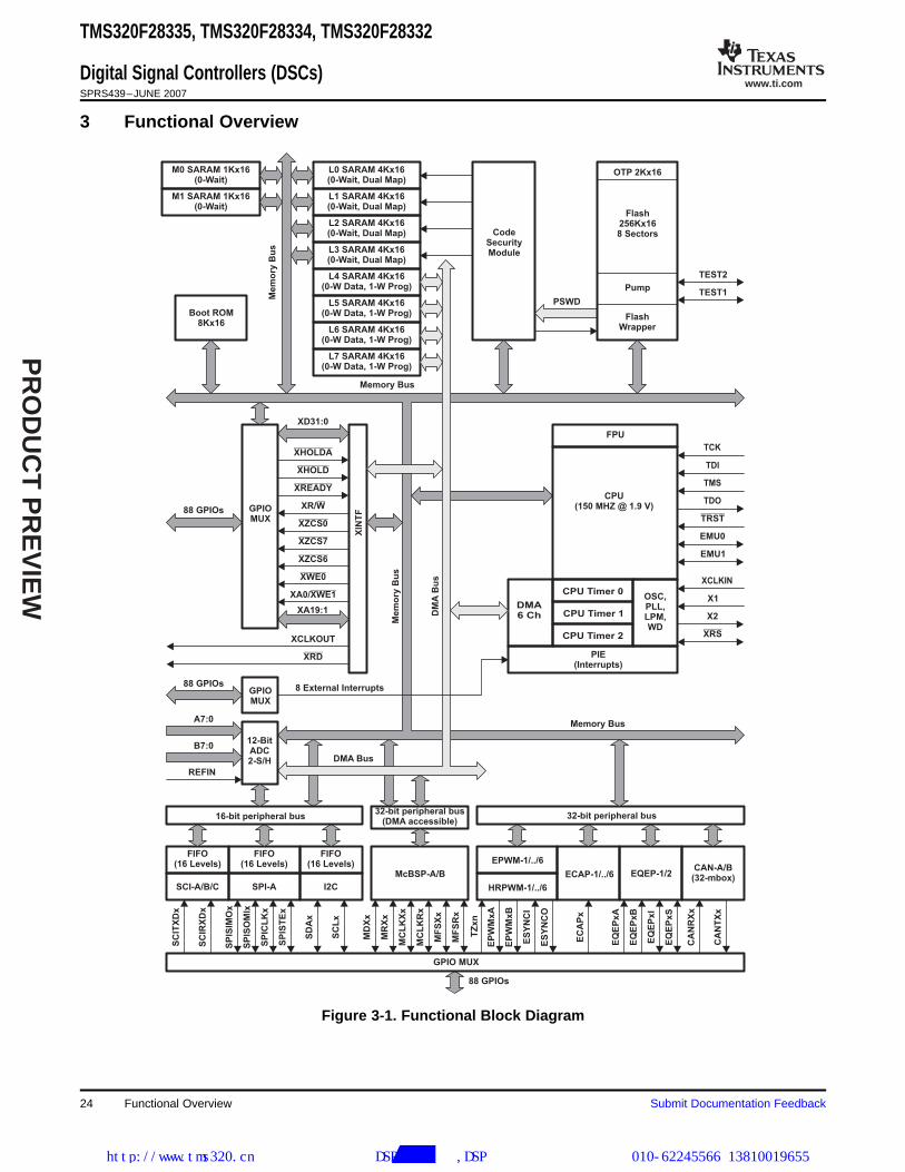
3 Functional Overview
M0 SARAM 1Kx16(0-Wait)
M1 SARAM 1Kx16(0-Wait)
L0 SARAM 4Kx16(0-Wait, Dual Map)
L1 SARAM 4Kx16(0-Wait, Dual Map)
L2 SARAM 4Kx16(0-Wait, Dual Map)
L3 SARAM 4Kx16(0-Wait, Dual Map)
L4 SARAM 4Kx16(0-W Data, 1-W Prog)
L5 SARAM 4Kx16(0-W Data, 1-W Prog)
L6 SARAM 4Kx16(0-W Data, 1-W Prog)
L7 SARAM 4Kx16(0-W Data, 1-W Prog)
Mem
ory
Bu
s
Boot ROM8Kx16
CodeSecurityModule
DM
AB
us
PSWD
OTP 2Kx16
Flash256Kx168 Sectors
Pump
FlashWrapper
TEST1
TEST2
XIN
TF
XA0/XWE1
XWE0
XZCS6
XZCS7
XZCS0
XR/W
XREADY
XHOLD
XHOLDA
XD31:0
XA19:1
GPIOMUX
Mem
ory
Bu
sMemory Bus
XCLKOUT
XRD
GPIOMUX
88 GPIOs8 External Interrupts
88 GPIOs
12-BitADC2-S/H
A7:0
B7:0
CPU Timer 0
CPU Timer 1
CPU Timer 2
OSC,PLL,LPM,WD
DMA6 Ch
PIE(Interrupts)
CPU(150 MHZ @ 1.9 V)
EMU1
EMU0
TRST
TDO
TMS
TDI
TCK
XRS
X2
X1
XCLKIN
FPU
REFIN
DMA Bus
Memory Bus
FIFO(16 Levels)
SCI-A/B/C
FIFO(16 Levels)
SPI-A
FIFO(16 Levels)
I2C
16-bit peripheral bus
SP
ISO
MIx
SP
ISIM
Ox
SP
ICL
Kx
SP
IST
Ex
SC
IRX
Dx
SC
ITX
Dx
SD
Ax
SC
Lx
McBSP-A/B
MR
Xx
MD
Xx
MC
LK
Xx
MC
LK
Rx
MF
SX
x
MF
SR
x
32-bit peripheral bus(DMA accessible)
EPWM-1/../6
HRPWM-1/../6
ECAP-1/../6 EQEP-1/2
EP
WM
xA
EP
WM
xB
ES
YN
CI
ES
YN
CO
TZ
xn
EC
AP
x
EQ
EP
xA
EQ
EP
xB
EQ
EP
xI
EQ
EP
xS
CAN-A/B(32-mbox)
CA
NR
Xx
CA
NT
Xx
32-bit peripheral bus
GPIO MUX
88 GPIOs
TMS320F28335, TMS320F28334, TMS320F28332
Digital Signal Controllers (DSCs)SPRS439–JUNE 2007
Figure 3-1. Functional Block Diagram
24 Functional Overview Submit Documentation Feedback
http://www.tms320.cn 提供DSP芯片解密,DSP破解等服务 010-62245566 13810019655

www.ti.com
PR
OD
UC
T P
RE
VIE
W
3.1 Memory Maps
TMS320F28335, TMS320F28334, TMS320F28332
Digital Signal Controllers (DSCs)SPRS439–JUNE 2007
In Figure 3-2 through Figure 3-4, the following apply:• Memory blocks are not to scale.• Peripheral Frame 0, Peripheral Frame 1, Peripheral Frame 2, and Peripheral Frame 3 memory maps
are restricted to data memory only. A user program cannot access these memory maps in programspace.
• Protected means the order of Write followed by Read operations is preserved rather than the pipelineorder.
• Certain memory ranges are EALLOW protected against spurious writes after configuration.
Submit Documentation Feedback Functional Overview 25
http://www.tms320.cn 提供DSP芯片解密,DSP破解等服务 010-62245566 13810019655

www.ti.com
PR
OD
UC
T P
RE
VIE
W
BlockStart Address
0x00 0000M0 Vector - RAM (32 x 32)
(Enable if VMAP = 0)
Data Space Prog Space
M0 SARAM (1K x 16)
M1 SARAM (1K x 16)
Peripheral Frame 0
0x00 0040
0x00 0400
0x00 0800
PIE Vector - RAM(256 x16)
(Enabled ifVMAP = 1,ENPIE =1)
Peripheral Frame 0
Reserved
Reserved
L0 SARAM (4K x16, Secure Zone Dual Mapped)
Peripheral Frame 1(Protected)
Reserved
Peripheral Frame 2(Protected)
L1 SARAM (4K x 16, Secure Zone Dual Mapped)
FLASH (256 K x 16, Secure Zone)
Reserved
Boot ROM (8K x 16)
BROM Vector - ROM (32 x 32)(Enable if VMAP = 1, ENPIE = 0)
0x00 0D00
0x00 0E00
0x00 2000
0x00 6000
0x00 7000
0x00 8000
0x00 9000
0x0001-0000
0x30 0000
0x3F C000
0x3F E000
0x3F FFC0
Data Space Prog Space
Reserved
XINTF Zone 6 (1 M x 16, )XZCS6
Reserved
XINTF Vector - RAM (32 x32)(Enable if VMAP = 1, ENPIR = 0)
On-Chip Memory External Memory XINTF
Only one of these vector maps*M0 vector, PIE vector, BROM vector, XINTF vector*should be enabled at a time.
LEGEND:
L2 SARAM (4Kx16, Secure Zone, Dual Mapped)
L3 SARAM (4Kx16, Secure Zone, Dual Mapped)
L4 SARAM (4Kx16, DMA Accessilbe)
L5 SARAM (4Kx16, DMA Accessible)
L6 SARAM (4Kx16, DMA Accessible)
L7 SARAM (4Kx16, DMA Accessiible)
0x0000-A000
0x0000-B000
0x0000-C000
0x0000-D000
0x0000-E000
0x0000-F000
Reserved
Reserved
0x10 0000
0x20 0000
XINTF Zone 0 (4K x 16, )(Protected, DMA Accessible)
XZCS00x00 4000
0x00 5000
0x30 0000
Lo
w 6
4K
(24x/2
40x E
qu
ivale
nt
Data
Sp
ace)
Hig
h 6
4K
(24x/2
40x E
qu
ivale
nt
Pro
gra
m S
pace)
0x00 5000
XINTF Zone 7 (1 M x 16, )XZCS7
Peripheral Frame 3 (Protected, DMA Accessable)
128-bit Password0x33 FFF8
0x34 0000
L0 SARAM (4K x 16, Secure Zone Dual Mapped)
OTP (IK x 16, Secure Zone)
0x3F 8000
Reserved
0x38 0400
L1 SARAM (4K x 16, Secure Zone Dual Mapped)0x3F 9000
L2 SARAM (4K x 16, Secure Zone Dual Mapped)0x3F A000
L3 SARAM (4K x 16, Secure Zone Dual Mapped)0x3F B000
TMS320F28335, TMS320F28334, TMS320F28332
Digital Signal Controllers (DSCs)SPRS439–JUNE 2007
Figure 3-2. F28335 Memory Map
Functional Overview26 Submit Documentation Feedback
http://www.tms320.cn 提供DSP芯片解密,DSP破解等服务 010-62245566 13810019655

www.ti.com
PR
OD
UC
T P
RE
VIE
W
BlockStart Address
0x00 0000M0 Vector - RAM (32 x 32)
(Enable if VMAP = 0)
Data Space Prog Space
M0 SARAM (1K x 16)
M1 SARAM (1K x 16)
Peripheral Frame 0
0x00 0040
0x00 0400
0x00 0800
PIE Vector - RAM(256 x16)
(Enabled ifVMAP = 1,ENPIE =1)
Peripheral Frame 0Reserved
Reserved
L0 SARAM (4K x16, Secure Zone Dual Mapped)
Peripheral Frame 1(Protected)
Reserved
Peripheral Frame 2(Protected)
L1 SARAM (4K x 16, Secure Zone Dual Mapped)
FLASH (128 K x 16, Secure Zone)
Reserved
Boot ROM (8K x 16)
BROM Vector - ROM (32 x 32)(Enable if VMAP = 1, ENPIE = 0)
0x00 0D00
0x00 0E00
0x00 2000
0x00 6000
0x00 7000
0x00 8000
0x00 9000
0x0001-0000
0x32 0000
0x3F C000
0x3F E000
0x3F FFC0
Data Space Prog Space
Reserved
XINTF Zone 0 (4K x 16, )(Protected, DMA Accessible)
XZCS0
XINTF Zone 6 (1 M x 16, )XZCS6
Reserved
XINTF Vector - RAM (32 x32)(Enable if VMAP = 1, ENPIR = 0)
On-Chip Memory External Memory XINTF
Only one of these vector maps*M0 vector, PIE vector, BROM vector, XINTF vector*should be enabled at a time.
LEGEND:
L2 SARAM (4Kx16, Secure Zone, Dual Mapped)
L3 SARAM (4Kx16, Secure Zone, Dual Mapped)
L4 SARAM (4Kx16, DMA Accessilbe)
L5 SARAM (4Kx16, DMA Accessible)
L6 SARAM (4Kx16, DMA Accessible)
L7 SARAM (4Kx16, DMA Accessiible)
0x0000-A000
0x0000-B000
0x0000-C000
0x0000-D000
0x0000-E000
0x0000-F000
Reserved
Reserved
0x00 4000
0x10 0000
0x20 0000
0x00 5000
0x30 0000
Lo
w 6
4K
(24x/2
40x E
qu
ivale
nt
Data
Sp
ace)
Hig
h 6
4K
(24x/2
40x E
qu
ivale
nt
Pro
gra
m S
pace)
0x00 5000
XINTF Zone 7 (1 M x 16, )XZCS7
Peripheral Frame 3 (Protected, DMA Accessable)
128-bit Password0x33 FFF8
0x34 0000
L0 SARAM (4K x 16, Secure Zone Dual Mapped)
OTP (IK x 16, Secure Zone)
0x3F 8000
Reserved
0x38 0400
L1 SARAM (4K x 16, Secure Zone Dual Mapped)0x3F 9000
L2 SARAM (4K x 16, Secure Zone Dual Mapped)0x3F A000
L3 SARAM (4K x 16, Secure Zone Dual Mapped)0x3F B000
XINTF Zone 7 (16K x 15, )(Enable if MP/ = 1)
XZCS6AND7MC
Peripheral Frame 0
TMS320F28335, TMS320F28334, TMS320F28332
Digital Signal Controllers (DSCs)SPRS439–JUNE 2007
Figure 3-3. F28334 Memory Map
Submit Documentation Feedback Functional Overview 27
http://www.tms320.cn 提供DSP芯片解密,DSP破解等服务 010-62245566 13810019655

www.ti.com
PR
OD
UC
T P
RE
VIE
W
BlockStart Address
0x00 0000M0 Vector - RAM (32 x 32)
(Enable if VMAP = 0)
Data Space Prog Space
M0 SARAM (1K x 16)
M1 SARAM (1K x 16)
Peripheral Frame 0
0x00 0040
0x00 0400
0x00 0800
PIE Vector - RAM(256 x16)
(Enabled ifVMAP = 1,ENPIE =1)
Reserved
Reserved
L0 SARAM (4K x16, Secure Zone Dual Mapped)
Peripheral Frame 1(Protected)
Reserved
Peripheral Frame 2(Protected)
L1 SARAM (4K x 16, Secure Zone Dual Mapped)
FLASH (64 K x 16, Secure Zone)
Reserved
Boot ROM (8K x 16)
BROM Vector - ROM (32 x 32)(Enable if VMAP = 1, ENPIE = 0)
0x00 0D00
0x00 0E00
0x00 2000
0x00 6000
0x00 7000
0x00 8000
0x00 9000
0x33 0000
0x3F C000
0x3F E000
0x3F FFC0
Data Space Prog Space
Reserved
XINTF Zone 0 (4K x 16, )(Protected, DMA Accessible)
XZCS0
XINTF Zone 6 (1 M x 16, )XZCS6
Reserved
XINTF Vector - RAM (32 x32)(Enable if VMAP = 1, ENPIR = 0)
On-Chip Memory External Memory XINTF
Only one of these vector maps*M0 vector, PIE vector, BROM vector, XINTF vector*should be enabled at a time.
LEGEND:
L2 SARAM (4Kx16, Secure Zone, Dual Mapped)
L3 SARAM (4Kx16, Secure Zone, Dual Mapped)
L4 SARAM (4Kx16, DMA Accessilbe)
L5 SARAM (4Kx16, DMA Accessible)
0x0000-A000
0x0000-B000
0x0000-C000
0x0000-D000
0x0000-E000
Reserved
Reserved
0x00 4000
0x10 0000
0x20 0000
0x00 5000
0x30 0000
Lo
w 6
4K
(24x/2
40x E
qu
ivale
nt
Data
Sp
ace)
Hig
h 6
4K
(24x/2
40x E
qu
ivale
nt
Pro
gra
m S
pace)
0x00 5000
XINTF Zone 7 (1 M x 16, )XZCS7
Peripheral Frame 3 (Protected, DMA Accessable)
128-bit Password0x33 FFF8
0x34 0000
L0 SARAM (4K x 16, Secure Zone Dual Mapped)
OTP (IK x 16, Secure Zone)
0x3F 8000
Reserved
0x38 0400
L1 SARAM (4K x 16, Secure Zone Dual Mapped)0x3F 9000
L2 SARAM (4K x 16, Secure Zone Dual Mapped)0x3F A000
L3 SARAM (4K x 16, Secure Zone Dual Mapped)0x3F B000
XINTF Zone 7 (16K x 15, )(Enable if MP/ = 1)
XZCS6AND7MC
Peripheral Frame 0
TMS320F28335, TMS320F28334, TMS320F28332
Digital Signal Controllers (DSCs)SPRS439–JUNE 2007
Figure 3-4. F28332 Memory Map
Functional Overview28 Submit Documentation Feedback
http://www.tms320.cn 提供DSP芯片解密,DSP破解等服务 010-62245566 13810019655

www.ti.com
PR
OD
UC
T P
RE
VIE
W
TMS320F28335, TMS320F28334, TMS320F28332
Digital Signal Controllers (DSCs)SPRS439–JUNE 2007
Table 3-1. Addresses of Flash Sectors in F28335
ADDRESS RANGE PROGRAM AND DATA SPACE
0x30 0000 - 0x30 7FFF Sector H (32K x 16)
0x30 8000 - 0x30 FFFF Sector G (32K x 16)
0x31 0000 - 0x31 7FFF Sector F (32K x 16)
0x31 8000 - 0x31 FFFF Sector E (32K x 16)
0x32 0000 - 0x32 7FFF Sector D (32K x 16)
0x32 8000 - 0x32 FFFF Sector C (32K x 16)
0x33 0000 - 0x33 7FFF Sector B (32K x 16)
0x33 8000 - 0x33 FFFF Sector A (32K x 16)
Program to 0x0000 when using the0x33 FF80 - 0x33 FFF5 Code Security Module
Boot-to-Flash Entry Point0x33 FFF6 - 0x33 FFF7 (program branch instruction here)
Security Password0x33 FFF8 - 0x33 FFFF (128-Bit) (Do Not Program to all zeros)
Table 3-2. Addresses of Flash Sectors in F28334
ADDRESS RANGE PROGRAM AND DATA SPACE
0x32 0000 - 0x32 3FFF Sector H (16K x 16)
0x32 4000 - 0x32 7FFF Sector G (16K x 16)
0x32 8000 - 0x32 BFFF Sector F (16K x 16)
0x32 C000 - 0x32 FFFF Sector E (16K x 16)
0x33 0000 - 0x33 3FFF Sector D (16K x 16)
0x33 4000 - 0x33 7FFFF Sector C (16K x 16)
0x33 8000 - 0x33 BFFF Sector B (16K x 16)
0x33 C000 - 0x33 FFFF Sector A (16K x 16)
0x33 FF80 - 0x33 FFF5 Program to 0x0000 when using theCode Security Module
0x33 FFF6 - 0x33 FFF7 Boot-to-Flash Entry Point(program branch instruction here)
0x33 FFF8 - 0x33 FFFF Security Password (128-Bit)(Do Not Program to all zeros)
Table 3-3. Addresses of Flash Sectors in F28332
ADDRESS RANGE PROGRAM AND DATA SPACE
0x33 0000 - 0x33 3FFF Sector D (16K x 16)
0x33 4000 - 0x33 7FFFF Sector C (16K x 16)
0x33 8000 - 0x33 BFFF Sector B (16K x 16)
0x33 C000 - 0x33 FFFF Sector A (16K x 16)
0x33 FF80 - 0x33 FFF5 Program to 0x0000 when using the Code SecurityModule
0x33 FFF6 - 0x33 FFF7 Boot-to-Flash Entry Point (program branchinstruction here)
0x33 FFF8 - 0x33 FFFF Security Password (128-Bit) (Do Not Program to allzeros)
Submit Documentation Feedback Functional Overview 29
http://www.tms320.cn 提供DSP芯片解密,DSP破解等服务 010-62245566 13810019655
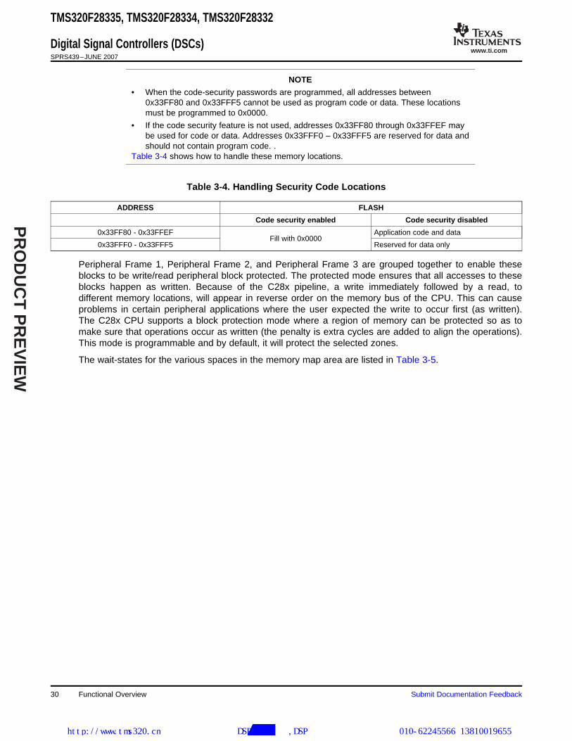
www.ti.com
PR
OD
UC
T P
RE
VIE
W
TMS320F28335, TMS320F28334, TMS320F28332
Digital Signal Controllers (DSCs)SPRS439–JUNE 2007
NOTE
• When the code-security passwords are programmed, all addresses between0x33FF80 and 0x33FFF5 cannot be used as program code or data. These locationsmust be programmed to 0x0000.
• If the code security feature is not used, addresses 0x33FF80 through 0x33FFEF maybe used for code or data. Addresses 0x33FFF0 – 0x33FFF5 are reserved for data andshould not contain program code. .
Table 3-4 shows how to handle these memory locations.
Table 3-4. Handling Security Code Locations
ADDRESS FLASH
Code security enabled Code security disabled
0x33FF80 - 0x33FFEF Application code and dataFill with 0x0000
0x33FFF0 - 0x33FFF5 Reserved for data only
Peripheral Frame 1, Peripheral Frame 2, and Peripheral Frame 3 are grouped together to enable theseblocks to be write/read peripheral block protected. The protected mode ensures that all accesses to theseblocks happen as written. Because of the C28x pipeline, a write immediately followed by a read, todifferent memory locations, will appear in reverse order on the memory bus of the CPU. This can causeproblems in certain peripheral applications where the user expected the write to occur first (as written).The C28x CPU supports a block protection mode where a region of memory can be protected so as tomake sure that operations occur as written (the penalty is extra cycles are added to align the operations).This mode is programmable and by default, it will protect the selected zones.
The wait-states for the various spaces in the memory map area are listed in Table 3-5.
30 Functional Overview Submit Documentation Feedback
http://www.tms320.cn 提供DSP芯片解密,DSP破解等服务 010-62245566 13810019655

www.ti.com
PR
OD
UC
T P
RE
VIE
W
TMS320F28335, TMS320F28334, TMS320F28332
Digital Signal Controllers (DSCs)SPRS439–JUNE 2007
Table 3-5. Wait-states
Area Wait-States CPU Comments
M0 and M1 SARAMs 0-wait Fixed
Peripheral Frame 0 1-wait (reads) This applies to all PF0 peripherals exceptthe floating-point unit (FPU) (0-wait reads)0-wait (writes)
Peripheral Frame 3 0-wait (writes) Assumes no conflicts between CPU andDMA.2-wait (reads)
Peripheral Frame 1 0-wait (writes) Cycles can be extended by peripheralgenerated ready.
2-wait (reads) Consecutive writes to the CAN willexperience a 1-cycle pipeline hit.
Peripheral Frame 2 0-wait (writes) Fixed. Cycles cannot be extended by theperipheral.2-wait (reads)
L0 SARAM 0-wait data and prog Assumes no CPU conflicts
L1 SARAM
L2 SARAM
L3 SARAM
L4 SARAM 0-wait data (read) Assumes no conflicts between CPU andDMA.L5 SARAM 0-wait data (write)
L6 SARAM 1-wait prog (read)
L7 SARAM 1-wait prog (write)
XINTF Programmable Programmed via the XTIMING registers orextendable via external XREADY signal.
1-wait minimum 1-wait is minimum wait states allowed onexternal waveforms for both reads andwrites on XINTF.
0-wait minimum writes with 0-wait minimum for writes assumes writewrite buffer enabled buffer enabled and not full.
Assumes no conflicts between CPU andDMA. When DMA and CPU attemptsimultaneous conflict, 1-cycle delay isadded for arbitration.
OTP Programmable Programmed via the Flash registers.
1-wait minimum 1-wait is minimum number of wait statesallowed. 1-wait-state operation is possibleat a reduced CPU frequency.
FLASH Programmable Programmed via the Flash registers.
1-wait Paged min 0-wait minimum for paged access is notallowed
1-wait Random min
Random > Paged
FLASH Password Programmable, Wait states of password locations arefixed.16-wait fixed
Boot-ROM 1-wait 0-wait speed is not possible.
Submit Documentation Feedback Functional Overview 31
http://www.tms320.cn 提供DSP芯片解密,DSP破解等服务 010-62245566 13810019655

www.ti.com
PR
OD
UC
T P
RE
VIE
W
3.2 Brief Descriptions
3.2.1 C28x CPU
3.2.2 Memory Bus (Harvard Bus Architecture)
3.2.3 Peripheral Bus
3.2.4 Real-Time JTAG and Analysis
TMS320F28335, TMS320F28334, TMS320F28332
Digital Signal Controllers (DSCs)SPRS439–JUNE 2007
The C28x™ DSC generation is the newest member of the TMS320C2000™ DSC platform. The C28x is avery efficient C/C++ engine, hence enabling users to develop not only their system control software in ahigh-level language, but also enables math algorithms to be developed using C/C++. The C28x is asefficient in DSC math tasks as it is in system control tasks that typically are handled by microcontrollerdevices. This efficiency removes the need for a second processor in many systems. The 32 x 32-bit MACcapabilities of the C28x and its 64-bit processing capabilities, enable the C28x to efficiently handle highernumerical resolution problems. Add to this the fast interrupt response with automatic context save ofcritical registers, resulting in a device that is capable of servicing many asynchronous events with minimallatency. The C28x has an 8-level-deep protected pipeline with pipelined memory accesses. This pipeliningenables the C28x to execute at high speeds without resorting to expensive high-speed memories. Specialbranch-look-ahead hardware minimizes the latency for conditional discontinuities. Special store conditionaloperations further improve performance.
As with many DSC type devices, multiple busses are used to move data between the memories andperipherals and the CPU. The C28x memory bus architecture contains a program read bus, data read busand data write bus. The program read bus consists of 22 address lines and 32 data lines. The data readand write busses consist of 32 address lines and 32 data lines each. The 32-bit-wide data busses enablesingle cycle 32-bit operations. The multiple bus architecture, commonly termed Harvard Bus, enables theC28x to fetch an instruction, read a data value and write a data value in a single cycle. All peripherals andmemories attached to the memory bus will prioritize memory accesses. Generally, the priority of memorybus accesses can be summarized as follows:
Highest: Data Writes (Simultaneous data and program writes cannot occur on the memory bus.)
Program Writes (Simultaneous data and program writes cannot occur on the memory bus.)
Data Reads
Program Reads (Simultaneous program reads and fetches cannot occur on the memory bus.)
Lowest: Fetches (Simultaneous program reads and fetches cannot occur on the memory bus.)
To enable migration of peripherals between various Texas Instruments (TI) DSC family of devices, the2833x devices adopt a peripheral bus standard for peripheral interconnect. The peripheral bus bridgemultiplexes the various busses that make up the processor Memory Bus into a single bus consisting of 16address lines and 16 or 32 data lines and associated control signals. Three versions of the peripheral busare supported on the 2833x. One version supports only 16-bit accesses (called peripheral frame 2).Another version supports both 16- and 32-bit accesses (called peripheral frame 1). The third versionsupports DMA access and both 16- and 32-bit accesses (called peripheral frame 3).
The 2833x implements the standard IEEE 1149.1 JTAG interface. Additionally, the 2833x supportsreal-time mode of operation whereby the contents of memory, peripheral and register locations can bemodified while the processor is running and executing code and servicing interrupts. The user can alsosingle step through non-time critical code while enabling time-critical interrupts to be serviced withoutinterference. The 2833x implements the real-time mode in hardware within the CPU. This is a uniquefeature to the 2833x, no software monitor is required. Additionally, special analysis hardware is providedwhich allows the user to set hardware breakpoint or data/address watch-points and generate varioususer-selectable break events when a match occurs.
Functional Overview32 Submit Documentation Feedback
http://www.tms320.cn 提供DSP芯片解密,DSP破解等服务 010-62245566 13810019655

www.ti.com
PR
OD
UC
T P
RE
VIE
W
3.2.5 External Interface (XINTF)
3.2.6 Flash
3.2.7 M0, M1 SARAMs
3.2.8 L0, L1, L2, L3, L4, L5, L6, L7 SARAMs
3.2.9 Boot ROM
TMS320F28335, TMS320F28334, TMS320F28332
Digital Signal Controllers (DSCs)SPRS439–JUNE 2007
This asynchronous interface consists of 19 address lines, 32 data lines, and three chip-select lines. Thechip-select lines are mapped to three external zones, Zones 0, 6, and 7. Each of the three zones can beprogrammed with a different number of wait states, strobe signal setup and hold timing and each zone canbe programmed for extending wait states externally or not. The programmable wait-state, chip-select andprogrammable strobe timing enables glueless interface to external memories and peripherals.
The F28335 contains 256K × 16 of embedded flash memory, segregated into eight 32K × 16 sectors. TheF28334 contains 128K × 16 of embedded flash memory, segregated into eight 16K × 16 sectors. TheF28332 device contains 64K ×16 of embedded flash, segregated into four 16K × 16 sectors. All thedevices also contain a single 1K × 16 of OTP memory at address range 0x380400 – 0x3807FF. The usercan individually erase, program, and validate a flash sector while leaving other sectors untouched.However, it is not possible to use one sector of the flash or the OTP to execute flash algorithms thaterase/program other sectors. Special memory pipelining is provided to enable the flash module to achievehigher performance. The flash/OTP is mapped to both program and data space; therefore, it can be usedto execute code or store data information. Note that addresses 0x33FFF0 – 0x33FFF5 are reserved fordata variables and should not contain program code.
NOTEThe F28335/F28334/F28332 Flash and OTP wait-states can be configured by theapplication. This allows applications running at slower frequencies to configure the flash touse fewer wait-states.
Flash effective performance can be improved by enabling the flash pipeline mode in theFlash options register. With this mode enabled, effective performance of linear codeexecution will be much faster than the raw performance indicated by the wait-stateconfiguration alone. The exact performance gain when using the Flash pipeline mode isapplication-dependent.
For more information on the Flash options, Flash wait-state, and OTP wait-state registers,see the TMS320x280x, 2801x, 2804x System Control and Interrupts Reference Guide(literature number SPRU712).
All 2833x devices contain these two blocks of single access memory, each 1K × 16 in size. The stackpointer points to the beginning of block M1 on reset. The M0 and M1 blocks, like all other memory blockson C28x devices, are mapped to both program and data space. Hence, the user can use M0 and M1 toexecute code or for data variables. The partitioning is performed within the linker. The C28x devicepresents a unified memory map to the programmer. This makes for easier programming in high-levellanguages.
The F28335 and F28334 each contain an additional 32K × 16 of single-access RAM, divided into 8 blocks(L0-L7 with 4K each). The F28332 contains an additional 24K × 16 of single-access RAM, divided into6 blocks (L0-L5 with 4K each). Each block can be independently accessed to minimize CPU pipelinestalls. Each block is mapped to both program and data space. L4, L5, L6, and L7 are DMA accessible
The Boot ROM is factory-programmed with boot-loading software. Boot-mode signals are provided to tellthe bootloader software what boot mode to use on power up. The user can select to boot normally or todownload new software from an external connection or to select boot software that is programmed in theinternal Flash/ROM. The Boot ROM also contains standard tables, such as SIN/COS waveforms, for usein math related algorithms.
Submit Documentation Feedback Functional Overview 33
http://www.tms320.cn 提供DSP芯片解密,DSP破解等服务 010-62245566 13810019655
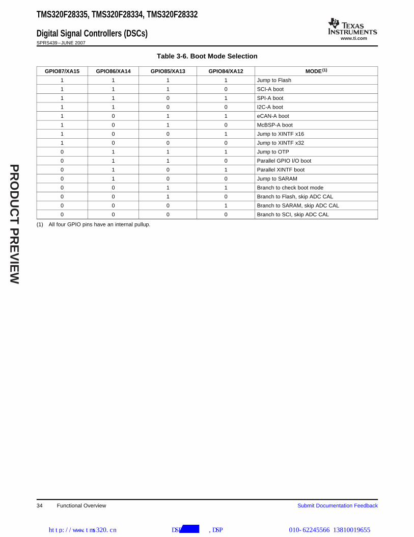
www.ti.com
PR
OD
UC
T P
RE
VIE
W
TMS320F28335, TMS320F28334, TMS320F28332
Digital Signal Controllers (DSCs)SPRS439–JUNE 2007
Table 3-6. Boot Mode Selection
GPIO87/XA15 GPIO86/XA14 GPIO85/XA13 GPIO84/XA12 MODE (1)
1 1 1 1 Jump to Flash
1 1 1 0 SCI-A boot
1 1 0 1 SPI-A boot
1 1 0 0 I2C-A boot
1 0 1 1 eCAN-A boot
1 0 1 0 McBSP-A boot
1 0 0 1 Jump to XINTF x16
1 0 0 0 Jump to XINTF x32
0 1 1 1 Jump to OTP
0 1 1 0 Parallel GPIO I/O boot
0 1 0 1 Parallel XINTF boot
0 1 0 0 Jump to SARAM
0 0 1 1 Branch to check boot mode
0 0 1 0 Branch to Flash, skip ADC CAL
0 0 0 1 Branch to SARAM, skip ADC CAL
0 0 0 0 Branch to SCI, skip ADC CAL
(1) All four GPIO pins have an internal pullup.
34 Functional Overview Submit Documentation Feedback
http://www.tms320.cn 提供DSP芯片解密,DSP破解等服务 010-62245566 13810019655

www.ti.com
PR
OD
UC
T P
RE
VIE
W
3.2.10 Security
3.2.11 Peripheral Interrupt Expansion (PIE) Block
TMS320F28335, TMS320F28334, TMS320F28332
Digital Signal Controllers (DSCs)SPRS439–JUNE 2007
The 2833x devices support high levels of security to protect the user firmware from being reverseengineered. The security features a 128-bit password (hardcoded for 16 wait-states), which the userprograms into the flash. One code security module (CSM) is used to protect the flash/OTP and theL0/L1/L2/L3 SARAM blocks. The security feature prevents unauthorized users from examining thememory contents via the JTAG port, executing code from external memory or trying to boot-load someundesirable software that would export the secure memory contents. To enable access to the secureblocks, the user must write the correct 128-bit KEY value, which matches the value stored in the passwordlocations within the Flash.
NOTE
• When the code-security passwords are programmed, all addresses between0x33FF80 and 0x33FFF5 cannot be used as program code or data. These locationsmust be programmed to 0x0000.
• If the code security feature is not used, addresses 0x33FF80 through 0x33FFEF maybe used for code or data. Addresses 0x33FFF0 – 0x33FFF5 are reserved for data andshould not contain program code. .
The 128-bit password (at 0x33 FFF8 – 0x33 FFFF) must not be programmed to zeros.Doing so would permanently lock the device.
NOTECode Security Module Disclaimer
THE CODE SECURITY MODULE (CSM) INCLUDED ON THIS DEVICE WASDESIGNED TO PASSWORD PROTECT THE DATA STORED IN THE ASSOCIATEDMEMORY (EITHER ROM OR FLASH) AND IS WARRANTED BY TEXASINSTRUMENTS (TI), IN ACCORDANCE WITH ITS STANDARD TERMS ANDCONDITIONS, TO CONFORM TO TI'S PUBLISHED SPECIFICATIONS FOR THEWARRANTY PERIOD APPLICABLE FOR THIS DEVICE.
TI DOES NOT, HOWEVER, WARRANT OR REPRESENT THAT THE CSM CANNOT BECOMPROMISED OR BREACHED OR THAT THE DATA STORED IN THE ASSOCIATEDMEMORY CANNOT BE ACCESSED THROUGH OTHER MEANS. MOREOVER,EXCEPT AS SET FORTH ABOVE, TI MAKES NO WARRANTIES ORREPRESENTATIONS CONCERNING THE CSM OR OPERATION OF THIS DEVICE,INCLUDING ANY IMPLIED WARRANTIES OF MERCHANTABILITY OR FITNESS FORA PARTICULAR PURPOSE.
IN NO EVENT SHALL TI BE LIABLE FOR ANY CONSEQUENTIAL, SPECIAL,INDIRECT, INCIDENTAL, OR PUNITIVE DAMAGES, HOWEVER CAUSED, ARISING INANY WAY OUT OF YOUR USE OF THE CSM OR THIS DEVICE, WHETHER OR NOTTI HAS BEEN ADVISED OF THE POSSIBILITY OF SUCH DAMAGES. EXCLUDEDDAMAGES INCLUDE, BUT ARE NOT LIMITED TO LOSS OF DATA, LOSS OFGOODWILL, LOSS OF USE OR INTERRUPTION OF BUSINESS OR OTHERECONOMIC LOSS.
The PIE block serves to multiplex numerous interrupt sources into a smaller set of interrupt inputs. ThePIE block can support up to 96 peripheral interrupts. On the 2833x, 58 of the possible 96 interrupts areused by peripherals. The 96 interrupts are grouped into blocks of 8 and each group is fed into 1 of 12
Submit Documentation Feedback Functional Overview 35
http://www.tms320.cn 提供DSP芯片解密,DSP破解等服务 010-62245566 13810019655

www.ti.com
PR
OD
UC
T P
RE
VIE
W
3.2.12 External Interrupts (XINT1-XINT7, XNMI)
3.2.13 Oscillator and PLL
3.2.14 Watchdog
3.2.15 Peripheral Clocking
3.2.16 Low-Power Modes
TMS320F28335, TMS320F28334, TMS320F28332
Digital Signal Controllers (DSCs)SPRS439–JUNE 2007
CPU interrupt lines (INT1 to INT12). Each of the 96 interrupts is supported by its own vector stored in adedicated RAM block that can be overwritten by the user. The vector is automatically fetched by the CPUon servicing the interrupt. It takes 8 CPU clock cycles to fetch the vector and save critical CPU registers.Hence the CPU can quickly respond to interrupt events. Prioritization of interrupts is controlled inhardware and software. Each individual interrupt can be enabled/disabled within the PIE block.
The 2833x supports eight masked external interrupts (XINT1-XINT7, XNMI). XNMI can be connected tothe INT13 or NMI interrupt of the CPU. Each of the interrupts can be selected for negative, positive, orboth negative and positive edge triggering and can also be enabled/disabled (including the XNMI). Themasked interrupts also contain a 16-bit free running up counter, which is reset to zero when a validinterrupt edge is detected. This counter can be used to accurately time stamp the interrupt. Unlike the281x devices, there are no dedicated pins for the external interrupts. Rather, any Port A GPIO pin can beconfigured to trigger any external interrupt.
The 2833x can be clocked by an external oscillator or by a crystal attached to the on-chip oscillator circuit.A PLL is provided supporting up to 10 input-clock-scaling ratios. The PLL ratios can be changed on-the-flyin software, enabling the user to scale back on operating frequency if lower power operation is desired.Refer to the Electrical Specification section for timing details. The PLL block can be set in bypass mode.
The 2833x devices contain a watchdog timer. The user software must regularly reset the watchdogcounter within a certain time frame; otherwise, the watchdog will generate a reset to the processor. Thewatchdog can be disabled if necessary.
The clocks to each individual peripheral can be enabled/disabled so as to reduce power consumptionwhen a peripheral is not in use. Additionally, the system clock to the serial ports (except I2C and eCAN)and the ADC blocks can be scaled relative to the CPU clock. This enables the timing of peripherals to bedecoupled from increasing CPU clock speeds.
The 2833x devices are full static CMOS devices. Three low-power modes are provided:
IDLE: Place CPU into low-power mode. Peripheral clocks may be turned off selectively and onlythose peripherals that need to function during IDLE are left operating. An enabled interruptfrom an active peripheral or the watchdog timer will wake the processor from IDLE mode.
STANDBY: Turns off clock to CPU and peripherals. This mode leaves the oscillator and PLL functional.An external interrupt event will wake the processor and the peripherals. Execution beginson the next valid cycle after detection of the interrupt event
HALT: Turns off the internal oscillator. This mode basically shuts down the device and places it inthe lowest possible power consumption mode. A reset or external signal can wake thedevice from this mode.
Functional Overview36 Submit Documentation Feedback
http://www.tms320.cn 提供DSP芯片解密,DSP破解等服务 010-62245566 13810019655

www.ti.com
PR
OD
UC
T P
RE
VIE
W
3.2.17 Peripheral Frames 0, 1, 2, 3 (PFn)
3.2.18 General-Purpose Input/Output (GPIO) Multiplexer
3.2.19 32-Bit CPU-Timers (0, 1, 2)
TMS320F28335, TMS320F28334, TMS320F28332
Digital Signal Controllers (DSCs)SPRS439–JUNE 2007
The 2833x device segregates peripherals into three sections. The mapping of peripherals is as follows:
PF0: PIE: PIE Interrupt Enable and Control Registers Plus PIE Vector Table
Flash: Flash Control, Programming, Erase, Verify Registers
XINTF: External Interface Registers
DMA DMA Registers
FPU: Floating-Point Unit Registers
Timers: CPU-Timers 0, 1, 2 Registers
CSM: Code Security Module KEY Registers
ADC: ADC Result Registers (dual-mapped)
PF1: eCAN: eCAN Mailbox and Control Registers
GPIO: GPIO MUX Configuration and Control Registers
ePWM: Enhanced Pulse Width Modulator Module and Registers
eCAP: Enhanced Capture Module and Registers
eQEP: Enhanced Quadrature Encoder Pulse Module and Registers
PF2: SYS: System Control Registers
SCI: Serial Communications Interface (SCI) Control and RX/TX Registers
SPI: Serial Port Interface (SPI) Control and RX/TX Registers
ADC: ADC Status, Control, and Result Register
I2C: Inter-Integrated Circuit Module and Registers
XINTF External Interface Registers
PF3: McBSP Multichannel Buffered Serial Port Registers
Most of the peripheral signals are multiplexed with general-purpose input/output (GPIO) signals. Thisenables the user to use a pin as GPIO if the peripheral signal or function is not used. On reset, GPIO pinsare configured as inputs. The user can individually program each pin for GPIO mode or peripheral signalmode. For specific inputs, the user can also select the number of input qualification cycles. This is to filterunwanted noise glitches. The GPIO signals can also be used to bring the device out of specific low-powermodes.
CPU-Timers 0, 1, and 2 are identical 32-bit timers with presettable periods and with 16-bit clockprescaling. The timers have a 32-bit count down register, which generates an interrupt when the counterreaches zero. The counter is decremented at the CPU clock speed divided by the prescale value setting.When the counter reaches zero, it is automatically reloaded with a 32-bit period value. CPU-Timer 2 isreserved for Real-Time OS (RTOS)/BIOS applications. CPU-Timer 1 is also reserved for TI systemfunctions. CPU-Timer 2 is connected to INT14 of the CPU. CPU-Timer 1 can be connected to INT13 ofthe CPU. CPU-Timer 0 is for general use and is connected to the PIE block.
Submit Documentation Feedback Functional Overview 37
http://www.tms320.cn 提供DSP芯片解密,DSP破解等服务 010-62245566 13810019655
www.ti.com
PR
OD
UC
T P
RE
VIE
W
3.2.20 Control Peripherals
3.2.21 Serial Port Peripherals
TMS320F28335, TMS320F28334, TMS320F28332
Digital Signal Controllers (DSCs)SPRS439–JUNE 2007
The 2833x devices support the following peripherals which are used for embedded control andcommunication:
ePWM: The enhanced PWM peripheral supports independent/complementary PWM generation,adjustable dead-band generation for leading/trailing edges, latched/cycle-by-cycle tripmechanism. Some of the PWM pins support HRPWM features.
eCAP: The enhanced capture peripheral uses a 32-bit time base and registers up to fourprogrammable events in continuous/one-shot capture modes.This peripheral can also be configured to generate an auxiliary PWM signal.
eQEP: The enhanced QEP peripheral uses a 32-bit position counter, supports low-speedmeasurement using capture unit and high-speed measurement using a 32-bit unit timer.This peripheral has a watchdog timer to detect motor stall and input error detection logicto identify simultaneous edge transition in QEP signals.
ADC: The ADC block is a 12-bit converter, single ended, 16-channels. It contains twosample-and-hold units for simultaneous sampling.
The 2833x devices support the following serial communication peripherals:
eCAN: This is the enhanced version of the CAN peripheral. It supports 32 mailboxes, timestamping of messages, and is CAN 2.0B-compliant.
McBSP: The multichannel buffered serial port (McBSP) connects to E1/T1 lines, phone-qualitycodecs for modem applications or high-quality stereo audio DAC devices. The McBSPreceive and transmit registers are supported by the DMA to significantly reduce theoverhead for servicing this peripheral.
SPI: The SPI is a high-speed, synchronous serial I/O port that allows a serial bit stream ofprogrammed length (one to sixteen bits) to be shifted into and out of the device at aprogrammable bit-transfer rate. Normally, the SPI is used for communications between theDSC and external peripherals or another processor. Typical applications include externalI/O or peripheral expansion through devices such as shift registers, display drivers, andADCs. Multi-device communications are supported by the master/slave operation of theSPI. On the 2833x, the SPI contains a 16-level receive and transmit FIFO for reducinginterrupt servicing overhead.
SCI: The serial communications interface is a two-wire asynchronous serial port, commonlyknown as UART. On the 2833x, the SCI contains a 16-level receive and transmit FIFO forreducing interrupt servicing overhead.
I2C: The inter-integrated circuit (I2C) module provides an interface between a DSC and otherdevices compliant with Philips Semiconductors Inter-IC bus (I2C-bus) specification version2.1 and connected by way of an I2C-bus. External components attached to this 2-wireserial bus can transmit/receive up to 8-bit data to/from the DSC through the I2C module.On the 2833x, the I2C contains a 16-level receive and transmit FIFO for reducing interruptservicing overhead.
Functional Overview38 Submit Documentation Feedback
http://www.tms320.cn 提供DSP芯片解密,DSP破解等服务 010-62245566 13810019655

www.ti.com
PR
OD
UC
T P
RE
VIE
W
3.3 Register Map
TMS320F28335, TMS320F28334, TMS320F28332
Digital Signal Controllers (DSCs)SPRS439–JUNE 2007
The 2833x devices contain four peripheral register spaces. The spaces are categorized as follows:
Peripheral These are peripherals that are mapped directly to the CPU memory bus.Frame 0: See Table 3-7
Peripheral These are peripherals that are mapped to the 32-bit peripheral bus.Frame 1 See Table 3-8
Peripheral These are peripherals that are mapped to the 16-bit peripheral bus.Frame 2: See Table 3-9
Peripheral These are peripherals that are mapped to the 32-bit DMA-accessible peripheralFrame 3: bus.
See Table 3-10
Table 3-7. Peripheral Frame 0 Registers (1)
NAME ADDRESS RANGE SIZE (×16) ACCESS TYPE (2)
Device Emulation Registers 0x00 0880 - 0x00 09FF 384 EALLOW protected
FLASH Registers (3) 0x00 0A80 - 0x00 0ADF 96 EALLOW protected
Code Security Module Registers 0x00 0AE0 - 0x00 0AEF 16 EALLOW protected
ADC registers (dual-mapped) (0 wait, read only) 0x00 0B00 - 0x00 0B1F 32 Not EALLOW protected
XINTF Registers 0x00 0B20 - 0x00 0B3F 32 Not EALLOW protected
CPU–TIMER0/1/2 Registers 0x00 0C00 - 0x00 0C3F 64 Not EALLOW protected
PIE Registers 0x00 0CE0 - 0x00 0CFF 32 Not EALLOW protected
PIE Vector Table 0x00 0D00 - 0x00 0DFF 256 EALLOW protected
DMA Registers 0x00 1000 - 0x00 11FF 512 EALLOW protected
(1) Registers in Frame 0 support 16-bit and 32-bit accesses.(2) If registers are EALLOW protected, then writes cannot be performed until the EALLOW instruction is executed. The EDIS instruction
disables writes to prevent stray code or pointers from corrupting register contents.(3) The Flash Registers are also protected by the Code Security Module (CSM).
Table 3-8. Peripheral Frame 1 Registers
NAME ADDRESS RANGE SIZE (×16)
ECAN-A Registers 0x0000 6000 - 0x0000 61FF 512
ECAN-B Registers 0x0000 6200 - 0x0000 63FF 512
EPWM1 + HRPWM1 Registers 0x0000 6800 - 0x0000 683F 64
EPWM2 + HRPWM2 Registers 0x0000 6840 - 0x0000 687F 64
EPWM3 + HRPWM3 Registers 0x0000 6880 - 0x0000 68BF 64
EPWM4 + HRPWM4 Registers 0x0000 68C0 - 0x0000 68FF 64
EPWM5 + HRPWM5 Registers 0x0000 6900 - 0x0000 693F 64
EPWM6 + HRPWM6 Registers 0x0000 6940 - 0x0000 697F 64
ECAP1 Registers 0x0000 6A00 - 0x0000 6A1F 32
ECAP2 Registers 0x0000 6A20 - 0x0000 6A3F 32
ECAP3 Registers 0x0000 6A40 - 0x0000 6A5F 32
ECAP4 Registers 0x0000 6A60 - 0x0000 6A7F 32
ECAP5 Registers 0x0000 6A80 - 0x0000 6A9F 32
ECAP6 Registers 0x0000 6AA0 - 0x0000 6ABF 32
EQEP1 Registers 0x0000 6B00 - 0x0000 6B3F 64
EQEP2 Registers 0x0000 6B40 - 0x0000 6B7F 64
GPIO Registers 0x0000 6F80 - 0x0000 6FFF 128
Submit Documentation Feedback Functional Overview 39
http://www.tms320.cn 提供DSP芯片解密,DSP破解等服务 010-62245566 13810019655

www.ti.com
PR
OD
UC
T P
RE
VIE
W
3.4 Device Emulation Registers
TMS320F28335, TMS320F28334, TMS320F28332
Digital Signal Controllers (DSCs)SPRS439–JUNE 2007
Table 3-9. Peripheral Frame 2 Registers
NAME ADDRESS RANGE SIZE (×16)
System Control Registers 0x0000 7010 - 0x0000 702F 32
SPI-A Registers 0x0000 7040 - 0x0000 704F 16
SCI-A Registers 0x0000 7050 - 0x0000 705F 16
External Interrupt Registers 0x0000 7070 - 0x0000 707F 16
ADC Registers 0x0000 7100 - 0x0000 711F 32
SCI-B Registers 0x0000 7750 - 0x0000 775F 16
SCI-C Registers 0x0000 7770 - 0x0000 777F 16
I2C-A Registers 0x0000 7900 - 0x0000 793F 64
Table 3-10. Peripheral Frame 3 Registers
NAME ADDRESS RANGE SIZE (×16)
McBSP-A Registers 0x0000 5000 - 0x0000 503F 64
McBSP-B Registers 0x0000 5040 - 0x0000 507F 64
These registers are used to control the protection mode of the C28x CPU and to monitor some criticaldevice signals. The registers are defined in Table 3-11.
Table 3-11. Device Emulation Registers
ADDRESSNAME SIZE (x16) DESCRIPTIONRANGE
0x0880DEVICECNF 2 Device Configuration Register0x0881
PARTID 0x0882 1 Part ID Register 0x00F8 (1) - F283320x00F9 - F283340x00FA - F28335
REVID 0x0883 1 Revision ID Register 0x0000 - Silicon Rev. 0 - TMX
PROTSTART 0x0884 1 Block Protection Start Address Register
PROTRANGE 0x0885 1 Block Protection Range Address Register
(1) The first byte (00) denotes flash devices. FF denotes ROM devices. Other values are reserved for future devices.
40 Functional Overview Submit Documentation Feedback
http://www.tms320.cn 提供DSP芯片解密,DSP破解等服务 010-62245566 13810019655

www.ti.com
PR
OD
UC
T P
RE
VIE
W
3.5 Interrupts
WDINT
LPMINTWatchdog
Low Power ModelsSync
SYSCLKOUT
WAKEINT
DMAClear
Peripherals(SPI, SCI, I2C, CAN, McBSP,EPWM, ECAP, EQEP, ADC)
DMA
XINT1Interrupt Control
XINT1CR(15:0)
XINT1CTR(15:0)
XINT1Latch
MU
X
GPIOXINT1SEL(4:0)
DMA
XINT2Interrupt Control
XINT2CR(15:0)
XINT2CTR(15:0)
XINT2
Latch
MU
X
GPIOXINT2SEL(4:0)
ADC XINT2SOC
DMA
TINT0CPU Timer 0
DMA
TINT2CPU Timer 2
CPU Timer 1
MU
X
TINT1
Flash Wrapper
TOUT1
Interrupt Control
XNMICR(15:0)
XNMICTR(15:0)
MU
X
1
DMA
NMI
INT13
INT14
INT1to
INT12
C28Core 9
6 I
nte
rru
pts
PIE
XNMI_XINT13
Latch
MU
X
GPIOXNMISEL(4:0)
GPIOMux
GPIO0.int
GPIO31.int
TMS320F28335, TMS320F28334, TMS320F28332
Digital Signal Controllers (DSCs)SPRS439–JUNE 2007
Figure 3-5 shows how the various interrupt sources are multiplexed within the 2833x devices.
Figure 3-5. External and PIE Interrupt Sources
Submit Documentation Feedback Functional Overview 41
http://www.tms320.cn 提供DSP芯片解密,DSP破解等服务 010-62245566 13810019655

www.ti.com
PR
OD
UC
T P
RE
VIE
W
Interrupt Control
XINT3CR(15:0)
Latch
Mu
x
GPIOXINT3SEL(4:0)
DMA
XINT3
Interrupt Control
XINT4CR(15:0)
Latch
Mu
x
GPIOXINT4SEL(4:0)
XINT4
Interrupt Control
XINT5CR(15:0)
Mu
x
GPIOXINT5SEL(4:0)
XINT5
Interrupt Control
XINT6CR(15:0)
Mu
x
GPIOXINT6SEL(4:0)
XINT6
Interrupt Control
XINT7CR(15:0)
Mu
x
GPIOXINT7SEL(4:0)
XINT7
DMA
DMA
DMA
DMA
96
In
terr
up
ts
PIE
INT1to
INT12
C28Core
GPIO32.int
GPIO63.int
GPIOMux
Latch
Latch
Latch
TMS320F28335, TMS320F28334, TMS320F28332
Digital Signal Controllers (DSCs)SPRS439–JUNE 2007
Figure 3-6. External Interrupts
Eight PIE block interrupts are grouped into one CPU interrupt. In total, 12 CPU interrupt groups, with 8interrupts per group equals 96 possible interrupts. On the 2833x, 58 of these are used by peripherals asshown in Table 3-12.
Functional Overview42 Submit Documentation Feedback
http://www.tms320.cn 提供DSP芯片解密,DSP破解等服务 010-62245566 13810019655

www.ti.com
PR
OD
UC
T P
RE
VIE
W
INT12
MUX
INT11
INT2INT1
CPU
(Enable)(Flag)
INTx
INTx.8
PIEIERx(8:1) PIEIFRx(8:1)
MUX
INTx.7INTx.6INTx.5INTx.4INTx.3INTx.2INTx.1
FromPeripherals or
ExternalInterrupts
(Enable) (Flag)
IER(12:1)IFR(12:1)
GlobalEnable
INTM
1
0
PIEACKx
(Enable/Flag)
TMS320F28335, TMS320F28334, TMS320F28332
Digital Signal Controllers (DSCs)SPRS439–JUNE 2007
Figure 3-7. Multiplexing of Interrupts Using the PIE Block
Table 3-12. PIE Peripheral Interrupts (1)
PIE INTERRUPTSCPUINTERRUPTS INTx.8 INTx.7 INTx.6 INTx.5 INTx.4 INTx.3 INTx.2 INTx.1
WAKEINT TINT0 ADCINT SEQ2INT SEQ1INTINT1 XINT2 XINT1 reserved(LPM/WD) (TIMER 0) (ADC) (ADC) (ADC)
EPWM6_TZINT EPWM5_TZINT EPWM4_TZINT EPWM3_TZINT EPWM2_TZINT EPWM1_TZINTINT2 reserved reserved (ePWM6) (ePWM5) (ePWM4) (ePWM3) (ePWM2) (ePWM1)
EPWM6_INT EPWM5_INT EPWM4_INT EPWM3_INT EPWM2_INT EPWM1_INTINT3 reserved reserved (ePWM6) (ePWM5) (ePWM4) (ePWM3) (ePWM2) (ePWM1)
ECAP6_INT ECAP5_INT ECAP4_INT ECAP3_INT ECAP2_INT ECAP1_INTINT4 reserved reserved (ECAP6) (ECAP5) (eCAP4) (eCAP3) (eCAP2) (eCAP1)
EQEP2_INT EQEP1_INTINT5 reserved reserved reserved reserved reserved reserved (eQEP2) (eQEP1)
MXINTA MRINTA MXINTB MRXINTB SPITXINTA SPIRXINTAINT6 reserved reserved (McBSP-A) (McBSP-A) (McBSP-B) (McBSP-B) (SPI-A) (SPI-A)
DINTCH6 DINTCH5 DINTCH4 DINTCH3 DINTCH2 DINTCH1INT7 reserved reserved (DMA) (DMA) (DMA) (DMA) (DMA) (DMA)
SCITXINTC SCIRXINTC I2CINT2A I2CINT1AINT8 reserved reserved reserved reserved(SCI-C) (SCI-C) (I2C-A) (I2C-A)
ECAN1_INTB ECAN0_INTB ECAN1_INTA ECAN0_INTA SCITXINTB SCIRXINTB SCITXINTA SCIRXINTAINT9 (CAN-B) (CAN-B) (CAN-A) (CAN-A) (SCI-B) (SCI-B) (SCI-A) (SCI-A)
INT10 reserved reserved reserved reserved reserved reserved reserved reserved
INT11 reserved reserved reserved reserved reserved reserved reserved reserved
LUF LVFINT12 reserved XINT7 XINT6 XINT5 XINT4 XINT3(FPU) (FPU)
(1) Out of the 96 possible interrupts, 58 interrupts are currently used. The remaining interrupts are reserved for future devices. Theseinterrupts can be used as software interrupts if they are enabled at the PIEIFRx level, provided none of the interrupts within the group isbeing used by a peripheral. Otherwise, interrupts coming in from peripherals may be lost by accidentally clearing their flag whilemodifying the PIEIFR. To summarize, there are two safe cases when the reserved interrupts could be used as software interrupts:1) No peripheral within the group is asserting interrupts.2) No peripheral interrupts are assigned to the group (example PIE group 11).
Submit Documentation Feedback Functional Overview 43
http://www.tms320.cn 提供DSP芯片解密,DSP破解等服务 010-62245566 13810019655

www.ti.com
PR
OD
UC
T P
RE
VIE
W
TMS320F28335, TMS320F28334, TMS320F28332
Digital Signal Controllers (DSCs)SPRS439–JUNE 2007
Table 3-13. PIE Configuration and Control Registers
NAME ADDRESS SIZE (X16) DESCRIPTION (1)
PIECTRL 0x0CE0 1 PIE, Control Register
PIEACK 0x0CE1 1 PIE, Acknowledge Register
PIEIER1 0x0CE2 1 PIE, INT1 Group Enable Register
PIEIFR1 0x0CE3 1 PIE, INT1 Group Flag Register
PIEIER2 0x0CE4 1 PIE, INT2 Group Enable Register
PIEIFR2 0x0CE5 1 PIE, INT2 Group Flag Register
PIEIER3 0x0CE6 1 PIE, INT3 Group Enable Register
PIEIFR3 0x0CE7 1 PIE, INT3 Group Flag Register
PIEIER4 0x0CE8 1 PIE, INT4 Group Enable Register
PIEIFR4 0x0CE9 1 PIE, INT4 Group Flag Register
PIEIER5 0x0CEA 1 PIE, INT5 Group Enable Register
PIEIFR5 0x0CEB 1 PIE, INT5 Group Flag Register
PIEIER6 0x0CEC 1 PIE, INT6 Group Enable Register
PIEIFR6 0x0CED 1 PIE, INT6 Group Flag Register
PIEIER7 0x0CEE 1 PIE, INT7 Group Enable Register
PIEIFR7 0x0CEF 1 PIE, INT7 Group Flag Register
PIEIER8 0x0CF0 1 PIE, INT8 Group Enable Register
PIEIFR8 0x0CF1 1 PIE, INT8 Group Flag Register
PIEIER9 0x0CF2 1 PIE, INT9 Group Enable Register
PIEIFR9 0x0CF3 1 PIE, INT9 Group Flag Register
PIEIER10 0x0CF4 1 PIE, INT10 Group Enable Register
PIEIFR10 0x0CF5 1 PIE, INT10 Group Flag Register
PIEIER11 0x0CF6 1 PIE, INT11 Group Enable Register
PIEIFR11 0x0CF7 1 PIE, INT11 Group Flag Register
PIEIER12 0x0CF8 1 PIE, INT12 Group Enable Register
PIEIFR12 0x0CF9 1 PIE, INT12 Group Flag Register
Reserved 0x0CFA 6 Reserved0x0CFF
(1) The PIE configuration and control registers are not protected by EALLOW mode. The PIE vector tableis protected.
44 Functional Overview Submit Documentation Feedback
http://www.tms320.cn 提供DSP芯片解密,DSP破解等服务 010-62245566 13810019655

www.ti.com
PR
OD
UC
T P
RE
VIE
W
3.5.1 External Interrupts
3.6 System Control
TMS320F28335, TMS320F28334, TMS320F28332
Digital Signal Controllers (DSCs)SPRS439–JUNE 2007
Table 3-14. External Interrupt Registers
Name Address Size (x16) Description
XINT1CR 0x0000 7070 1 XINT1 configuration register
XINT2CR 0x0000 7071 1 XINT2 configuration register
XINT3CR 0x0000 7072 1 XINT3 configuration register
XINT4CR 0x0000 7073 1 XINT4 configuration register
XINT5CR 0x0000 7074 1 XINT5 configuration register
XINT6CR 0x0000 7075 1 XINT6 configuration register
XINT7CR 0x0000 7076 1 XINT7 configuration register
XNMICR 0x0000 7077 1 XNMI configuration register
XINT1CTR 0x0000 7078 1 XINT1 counter register
XINT2CTR 0x0000 7079 1 XINT2 counter register
reserved 0x0000 707A - 0x0000 5707E
XNMICTR 0x0000 707F 1 XNMI counter register
Each external interrupt can be enabled/disabled or qualified using positive, negative, or both positive andnegative edge. For more information, see the TMS320x280x, 2801x, 2804x System Control and InterruptsReference Guide (literature number SPRU712).
This section describes the 2833x oscillator, PLL and clocking mechanisms, the watchdog function and thelow power modes. Figure 3-8 shows the various clock and reset domains in the 2833x devices that will bediscussed.
Submit Documentation Feedback Functional Overview 45
http://www.tms320.cn 提供DSP芯片解密,DSP破解等服务 010-62245566 13810019655

www.ti.com
PR
OD
UC
T P
RE
VIE
W
EPWM1/../6, HRPWM1/../6,ECAP1/../6, EQEP1/2
PeripheralRegisters
Bridge
Clock Enables
I/O
PeripheralRegisters
Clock Enables
I/O
eCAN-A/B
/2
PeripheralRegisters
Clock Enables
I/O
SPI-A, SCI-A/B/C, I2C-A
LOSPCPLSPCLK
SystemControlRegister
Bridge
SYSCLKOUT
Me
mo
ry B
us
C28x Core
GPIOMux
Clock Enables
PeripheralRegisters
I/O
McBSP-A/B
LOSPCPLSPCLK
Clock Enables
Bridge
HISPCPHSPCLK
DM
AB
us
ResultRegisters
Bridge
12-Bit ADCADC
Registers
16 Channels
DMAClock Enables
Pe
rip
he
ral
Bu
s
TMS320F28335, TMS320F28334, TMS320F28332
Digital Signal Controllers (DSCs)SPRS439–JUNE 2007
A. CLKIN is the clock into the CPU. It is passed out of the CPU as SYSCLKOUT (that is, CLKIN is the same frequencyas SYSCLKOUT).
Figure 3-8. Clock and Reset Domains
Functional Overview46 Submit Documentation Feedback
http://www.tms320.cn 提供DSP芯片解密,DSP破解等服务 010-62245566 13810019655

www.ti.com
PR
OD
UC
T P
RE
VIE
W
3.6.1 OSC and PLL Block
X1
XCLKIN (3.3-V clock input)
On chiposcillator
X2
xor
PLLSTS[OSCOFF]
OSCCLK
PLLVCOCLK
4-bit PLL Select (PLLCR)
OSCCLK or VCOCLK CLKIN
OSCCLK0
PLLSTS[PLLOFF]
n n ≠ 0 /2
PLLSTS[CLKINDIV]
TMS320F28335, TMS320F28334, TMS320F28332
Digital Signal Controllers (DSCs)SPRS439–JUNE 2007
The PLL, clocking, watchdog and low-power modes, are controlled by the registers listed in Table 3-15.
Table 3-15. PLL, Clocking, Watchdog, and Low-Power Mode Registers
Name Address Size (x16) Description
XCLK 0x0000-7010 1 XCLKOUT Pin Control and X1/XCLKIN Status Register
PLLSTS 0x0000-7011 1 PLL Status Register
reserved 0x0000-7012 - 0x0000-7018 7
HISPCP 0x0000-701A 1 High-Speed Peripheral Clock Pre-Scaler Register
LOSPCP 0x0000-701B 1 Low-Speed Peripheral Clock Pre-Scaler Register
PCLKCR0 0x0000-701C 1 Peripheral Clock Control Register 0
PCLKCR1 0x0000-701D 1 Peripheral Clock Control Register 1
LPMCR0 0x0000-701E 1 Low Power Mode Control Register 0
reserved 0x0000-701F 1 Low Power Mode Control Register 1
PCLKCR3 0x0000-7020 1 Peripheral Clock Control Register 3
PLLCR 0x0000-7021 1 PLL Control Register
SCSR 0x0000-7022 1 System Control and Status Register
WDCNTR 0x0000-7023 1 Watchdog Counter Register
reserved 0x0000-7024 1
WDKEY 0x0000-7025 1 Watchdog Reset Key Register
reserved 0x0000-7026 - 0x0000-7028 3
WDCR 0x0000-7029 1 Watchdog Control Register
reserved 0x0000-702A - 0x0000-702F 6
Figure 3-9 shows the OSC and PLL block on the 2833x.
Figure 3-9. OSC and PLL Block Diagram
The on-chip oscillator circuit enables a crystal/resonator to be attached to the 2833x devices using the X1and X2 pins. If the on-chip oscillator is not used, an external oscillator can be used in either one of thefollowing configurations:
1. A 3.3-V external oscillator can be directly connected to the XCLKIN pin. The X2 pin should be leftunconnected and the X1 pin tied low. The logic-high level in this case should not exceed VDDIO.
2. A 1.8-V external oscillator can be directly connected to the X1 pin. The X2 pin should be leftunconnected and the XCLKIN pin tied low. The logic-high level in this case should not exceed VDD.
The three possible input-clock configurations are shown in Figure 3-10 through Figure 3-12
Submit Documentation Feedback Functional Overview 47
http://www.tms320.cn 提供DSP芯片解密,DSP破解等服务 010-62245566 13810019655

www.ti.com
PR
OD
UC
T P
RE
VIE
W
External Clock Signal (Toggling 0 −VDDIO)
XCLKIN X2
NC
X1
External Clock Signal (Toggling 0 −VDD)
XCLKIN X2
NC
X1
CL1
X2X1
CrystalCL2
XCLKIN
TMS320F28335, TMS320F28334, TMS320F28332
Digital Signal Controllers (DSCs)SPRS439–JUNE 2007
Figure 3-10. Using a 3.3-V External Oscillator
Figure 3-11. Using a 1.8-V External Oscillator
Figure 3-12. Using the Internal Oscillator
3.6.1.1 External Reference Oscillator Clock Option
The typical specifications for the external quartz crystal for a frequency of 20 MHz are listed below:• Fundamental mode, parallel resonant• CL (load capacitance) = 12 pF• CL1 = CL2 = 24 pF• Cshunt = 6 pF• ESR range = 30 to 60 Ω
TI recommends that customers have the resonator/crystal vendor characterize the operation of theirdevice with the DSC chip. The resonator/crystal vendor has the equipment and expertise to tune the tankcircuit. The vendor can also advise the customer regarding the proper tank component values that willproduce proper start up and stability over the entire operating range.
3.6.1.2 PLL-Based Clock Module
The 2833x devices have an on-chip, PLL-based clock module. This module provides all the necessaryclocking signals for the device, as well as control for low-power mode entry. The PLL has a 4-bit ratiocontrol PLLCR[DIV] to select different CPU clock rates. The watchdog module should be disabled beforewriting to the PLLCR register. It can be re-enabled (if need be) after the PLL module has stabilized, whichtakes 131072 OSCCLK cycles.
48 Functional Overview Submit Documentation Feedback
http://www.tms320.cn 提供DSP芯片解密,DSP破解等服务 010-62245566 13810019655

www.ti.com
PR
OD
UC
T P
RE
VIE
W
TMS320F28335, TMS320F28334, TMS320F28332
Digital Signal Controllers (DSCs)SPRS439–JUNE 2007
Table 3-16. PLLCR Register Bit Definitions
SYSCLKOUTPLLCR[DIV] (1)(CLKIN) (2)
0000 (PLL bypass) OSCCLK/n
0001 (OSCCLK*1)/n
0010 (OSCCLK*2)/n
0011 (OSCCLK*3)/n
0100 (OSCCLK*4)/n
0101 (OSCCLK*5)/n
0110 (OSCCLK*6)/n
0111 (OSCCLK*7)/n
1000 (OSCCLK*8)/n
1001 (OSCCLK*9)/n
1010 (OSCCLK*10)/n
1011-1111 reserved
(1) This register is EALLOW protected.(2) CLKIN is the input clock to the CPU. SYSCLKOUT is the output
clock from the CPU. The frequency of SYSCLKOUT is the same asCLKIN. If CLKINDIV = 0, n = 2; if CLKINDIV = 1, n = 1.
Table 3-17. CLKIN Divide Options
PLLSTS [DIVSEL] CLKIN DIVIDE
0 /4
1 /4
2 /2
3 /1
The PLL-based clock module provides two modes of operation:• Crystal-operation - This mode allows the use of an external crystal/resonator to provide the time base
to the device.• External clock source operation - This mode allows the internal oscillator to be bypassed. The device
clocks are generated from an external clock source input on the X1 or the XCLKIN pin.
Table 3-18. Possible PLL Configuration Modes
SYSCLKOUTPLL MODE REMARKS PLLSTS[CLKINDIV] (CLKIN)
Invoked by the user setting the PLLOFF bit in the PLLSTS register. The PLL block 0 OSCCLK/2is disabled in this mode. This can be useful to reduce system noise and for low
PLL Off power operation. The PLLCR register must first be set to 0x0000 (PLL Bypass)1 OSCCLKbefore entering this mode. The CPU clock (CLKIN) is derived directly from the
input clock on either X1/X2, X1 or XCLKIN.
PLL Bypass is the default PLL configuration upon power-up or after an external 0 OSCCLK/2reset (XRS). This mode is selected when the PLLCR register is set to 0x0000 orPLL Bypass while the PLL locks to a new frequency after the PLLCR register has been 1 OSCCLKmodified. In this mode, the PLL itself is bypassed but the PLL is not turned off.
Achieved by writing a non-zero value n into the PLLCR register. Upon writing to thePLL Enable 0 OSCCLK*n/2PLLCR the device will switch to PLL Bypass mode until the PLL locks.
Submit Documentation Feedback Functional Overview 49
http://www.tms320.cn 提供DSP芯片解密,DSP破解等服务 010-62245566 13810019655
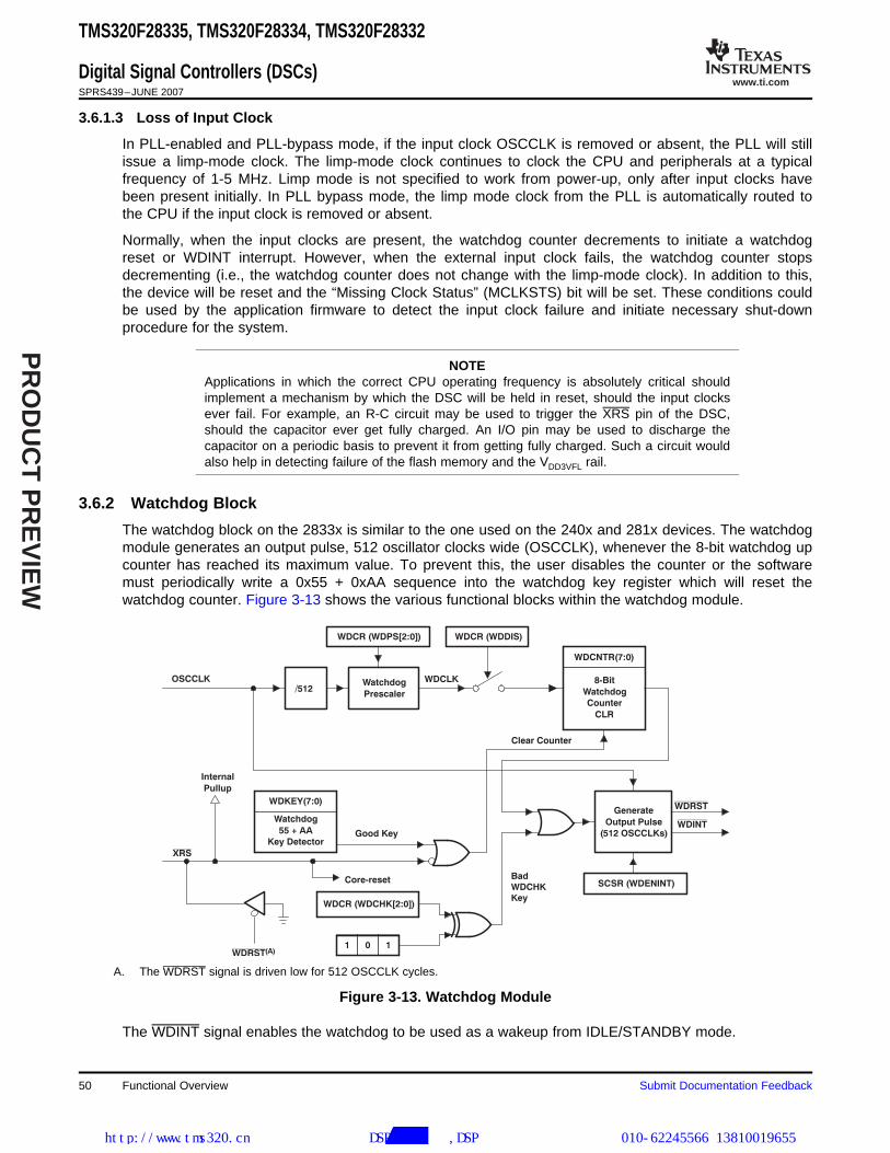
www.ti.com
PR
OD
UC
T P
RE
VIE
W
3.6.2 Watchdog Block
/512OSCCLK
WDCR (WDPS[2:0])
WDCLK
WDCNTR(7:0)
WDKEY(7:0)
Good Key
1 0 1
WDCR (WDCHK[2:0])
Bad
WDCHK
Key
WDCR (WDDIS)
Clear Counter
SCSR (WDENINT)
Watchdog
Prescaler
Generate
Output Pulse
(512 OSCCLKs)
8-Bit
Watchdog
Counter
CLR
WDRST
WDINTWatchdog
55 + AA
Key Detector
XRS
Core-reset
WDRST(A)
Internal
Pullup
TMS320F28335, TMS320F28334, TMS320F28332
Digital Signal Controllers (DSCs)SPRS439–JUNE 2007
3.6.1.3 Loss of Input Clock
In PLL-enabled and PLL-bypass mode, if the input clock OSCCLK is removed or absent, the PLL will stillissue a limp-mode clock. The limp-mode clock continues to clock the CPU and peripherals at a typicalfrequency of 1-5 MHz. Limp mode is not specified to work from power-up, only after input clocks havebeen present initially. In PLL bypass mode, the limp mode clock from the PLL is automatically routed tothe CPU if the input clock is removed or absent.
Normally, when the input clocks are present, the watchdog counter decrements to initiate a watchdogreset or WDINT interrupt. However, when the external input clock fails, the watchdog counter stopsdecrementing (i.e., the watchdog counter does not change with the limp-mode clock). In addition to this,the device will be reset and the “Missing Clock Status” (MCLKSTS) bit will be set. These conditions couldbe used by the application firmware to detect the input clock failure and initiate necessary shut-downprocedure for the system.
NOTEApplications in which the correct CPU operating frequency is absolutely critical shouldimplement a mechanism by which the DSC will be held in reset, should the input clocksever fail. For example, an R-C circuit may be used to trigger the XRS pin of the DSC,should the capacitor ever get fully charged. An I/O pin may be used to discharge thecapacitor on a periodic basis to prevent it from getting fully charged. Such a circuit wouldalso help in detecting failure of the flash memory and the VDD3VFL rail.
The watchdog block on the 2833x is similar to the one used on the 240x and 281x devices. The watchdogmodule generates an output pulse, 512 oscillator clocks wide (OSCCLK), whenever the 8-bit watchdog upcounter has reached its maximum value. To prevent this, the user disables the counter or the softwaremust periodically write a 0x55 + 0xAA sequence into the watchdog key register which will reset thewatchdog counter. Figure 3-13 shows the various functional blocks within the watchdog module.
A. The WDRST signal is driven low for 512 OSCCLK cycles.
Figure 3-13. Watchdog Module
The WDINT signal enables the watchdog to be used as a wakeup from IDLE/STANDBY mode.
Functional Overview50 Submit Documentation Feedback
http://www.tms320.cn 提供DSP芯片解密,DSP破解等服务 010-62245566 13810019655

www.ti.com
PR
OD
UC
T P
RE
VIE
W
3.7 Low-Power Modes Block
TMS320F28335, TMS320F28334, TMS320F28332
Digital Signal Controllers (DSCs)SPRS439–JUNE 2007
In STANDBY mode, all peripherals are turned off on the device. The only peripheral that remainsfunctional is the watchdog. The WATCHDOG module will run off OSCCLK. The WDINT signal is fed to theLPM block so that it can wake the device from STANDBY (if enabled). See Section Section 3.7,Low-Power Modes Block, for more details.
In IDLE mode, the WDINT signal can generate an interrupt to the CPU, via the PIE, to take the CPU out ofIDLE mode.
In HALT mode, this feature cannot be used because the oscillator (and PLL) are turned off and hence sois the WATCHDOG.
The low-power modes on the 2833x are similar to the 240x devices. Table 3-19 summarizes the variousmodes.
Table 3-19. Low-Power Modes
MODE LPMCR0(1:0) OSCCLK CLKIN SYSCLKOUT EXIT (1)
XRS, Watchdog interrupt, any enabledIDLE 00 On On On (2)interrupt, XNMI
On XRS, Watchdog interrupt, GPIO Port ASTANDBY 01 Off Off(watchdog still running) signal, debugger (3), XNMI
Off XRS, GPIO Port A signal, XNMI,HALT 1X (oscillator and PLL turned off, Off Off debugger (3)watchdog not functional)
(1) The Exit column lists which signals or under what conditions the low power mode will be exited. A low signal, on any of the signals, willexit the low power condition. This signal must be kept low long enough for an interrupt to be recognized by the device. Otherwise theIDLE mode will not be exited and the device will go back into the indicated low power mode.
(2) The IDLE mode on the C28x behaves differently than on the 24x/240x. On the C28x, the clock output from the CPU (SYSCLKOUT) isstill functional while on the 24x/240x the clock is turned off.
(3) On the C28x, the JTAG port can still function even if the CPU clock (CLKIN) is turned off.
The various low-power modes operate as follows:
IDLE Mode: This mode is exited by any enabled interrupt or an XNMI that is recognized bythe processor. The LPM block performs no tasks during this mode as long as theLPMCR0(LPM) bits are set to 0,0.
STANDBY Mode: Any GPIO port A signal (GPIO[31:0]) can wake the device from STANDBYmode. The user must select which signal(s) will wake the device in theGPIOLPMSEL register. The selected signal(s) are also qualified by the OSCCLKbefore waking the device. The number of OSCCLKs is specified in the LPMCR0register.
HALT Mode: Only the XRS and any GPIO port A signal (GPIO[31:0]) can wake the devicefrom HALT mode. The user selects the signal in the GPIOLPMSEL register.
NOTEThe low-power modes do not affect the state of the output pins (PWM pins included).They will be in whatever state the code left them in when the IDLE instruction wasexecuted. See the TMS320x280x, 2801x, 2804x System Control and Interrupts ReferenceGuide (literature number SPRU712) for more details.
Submit Documentation Feedback Functional Overview 51
http://www.tms320.cn 提供DSP芯片解密,DSP破解等服务 010-62245566 13810019655
www.ti.com
PR
OD
UC
T P
RE
VIE
W
4 Peripherals
TMS320F28335, TMS320F28334, TMS320F28332
Digital Signal Controllers (DSCs)SPRS439–JUNE 2007
The integrated peripherals of the 2833x are described in the following subsections:• Three 32-bit CPU-Timers• Up to six enhanced PWM modules (ePWM1, ePWM2, ePWM3, ePWM4, ePWM5, ePWM6)• Up to six enhanced capture modules (eCAP1, eCAP2, eCAP3, eCAP4, eCAP5, eCAP6)• Up to two enhanced QEP modules (eQEP1, eQEP2)• Enhanced analog-to-digital converter (ADC) module• Up to two enhanced controller area network (eCAN) modules (eCAN-A, eCAN-B)• Up to three serial communications interface modules (SCI-A, SCI-B, SCI-C)• One serial peripheral interface (SPI) module (SPI-A)• Inter-integrated circuit module (I2C)• Up to two multichannel buffered serial port (McBSP-A, McBSP-B) modules• Digital I/O and shared pin functions
52 Peripherals Submit Documentation Feedback
http://www.tms320.cn 提供DSP芯片解密,DSP破解等服务 010-62245566 13810019655

www.ti.com
PR
OD
UC
T P
RE
VIE
W
4.1 DMA Overview
PIE
Peripheral Bus
DIN
T[C
H1
:CH
6]
Memory Bus
ADC0/1-wait
Registers(16 x 16)
SY
SC
LK
OU
T
DM
AE
ve
nt
Tri
gg
ers
Du
al
Po
rts
Du
al
Po
rt
XIN
TF
Du
al
Po
rt
AD
CC
on
tro
l
CP
U
L4SARAM(4K x 16) M
cB
SP
-B
Mc
BS
P-A
Ex
tern
al
Inte
rru
pts
DMA Bus
L5SARAM(4K x 16)
CP
U T
ime
rs
L6SARAM(4K x 16)
L7SARAM(4K x 16)
DMAType 0
6-Ch
TMS320F28335, TMS320F28334, TMS320F28332
Digital Signal Controllers (DSCs)SPRS439–JUNE 2007
Features:• 6 Channels with independent PIE interrupts• Trigger Sources:
– ADC Sequencer 1 and Sequencer 2– McBSP-A and McBSP-B transmit and receive logic– XINT1-7 and XINT13– CPU Timers– Software
• Data Sources/Destinations:– L4-L7 16k x 16 SARAM– All XINTF zones– ADC Memory Bus mapped RESULT registers– McBSP-A and McBSP-B transmit and receive buffers
• Word Size: 16-bit or 32-bit (McBSPs limited to 16-bit)• Throughput: 4 cycles/word (5 cycles/word for McBSP reads)
Figure 4-1. DMA Functional Block Diagram
Submit Documentation Feedback Peripherals 53
http://www.tms320.cn 提供DSP芯片解密,DSP破解等服务 010-62245566 13810019655

www.ti.com
PR
OD
UC
T P
RE
VIE
W
4.2 32-Bit CPU-Timers 0/1/2
Borrow
Reset
Timer Reload
SYSCLKOUTTCR.4
(Timer Start Status)
TINT
16-Bit Timer Divide-Down TDDRH:TDDR
32-Bit Timer PeriodPRDH:PRD
32-Bit CounterTIMH:TIM
16-Bit Prescale CounterPSCH:PSC
Borrow
INT1to
INT12
INT14
C28x
TINT2
TINT0PIE CPU-TIMER 0
CPU-TIMER 2 (Reserved for
DSP/BIOS)
INT13TINT1 CPU-TIMER 1
(Reserved for TI system functions)
XINT13
TMS320F28335, TMS320F28334, TMS320F28332
Digital Signal Controllers (DSCs)SPRS439–JUNE 2007
There are three 32-bit CPU-timers on the 2833x devices (CPU-TIMER0/1/2).
CPU-Timer 1 is reserved for TI system functions and Timer 2 is reserved for DSP/BIOS™. CPU-Timer 0can be used in user applications. These timers are different from the timers that are present in the ePWMmodules.
NOTENOTE: If the application is not using DSP/BIOS, then CPU-Timer 2 can be used in theapplication.
Figure 4-2. CPU-Timers
In the 2833x devices, the timer interrupt signals (TINT0, TINT1, TINT2) are connected as shown inFigure 4-3.
A. The timer registers are connected to the memory bus of the C28x processor.
B. The timing of the timers is synchronized to SYSCLKOUT of the processor clock.
C. While TIMER1 is reserved, INT13 is not reserved and the user can use XINT13 connected to INT13.
Figure 4-3. CPU-Timer Interrupt Signals and Output Signal
Peripherals54 Submit Documentation Feedback
http://www.tms320.cn 提供DSP芯片解密,DSP破解等服务 010-62245566 13810019655

www.ti.com
PR
OD
UC
T P
RE
VIE
W
TMS320F28335, TMS320F28334, TMS320F28332
Digital Signal Controllers (DSCs)SPRS439–JUNE 2007
The general operation of the timer is as follows: The 32-bit counter register "TIMH:TIM" is loaded with thevalue in the period register "PRDH:PRD". The counter register decrements at the SYSCLKOUT rate of theC28x. When the counter reaches 0, a timer interrupt output signal generates an interrupt pulse. Theregisters listed in Table 4-1 are used to configure the timers. For more information, see the TMS320x280x,2801x, 2804x System Control and Interrupts Reference Guide (literature number SPRU712).
Table 4-1. CPU-Timers 0, 1, 2 Configuration and Control Registers
NAME ADDRESS SIZE (x16) DESCRIPTION
TIMER0TIM 0x0C00 1 CPU-Timer 0, Counter Register
TIMER0TIMH 0x0C01 1 CPU-Timer 0, Counter Register High
TIMER0PRD 0x0C02 1 CPU-Timer 0, Period Register
TIMER0PRDH 0x0C03 1 CPU-Timer 0, Period Register High
TIMER0TCR 0x0C04 1 CPU-Timer 0, Control Register
reserved 0x0C05 1
TIMER0TPR 0x0C06 1 CPU-Timer 0, Prescale Register
TIMER0TPRH 0x0C07 1 CPU-Timer 0, Prescale Register High
TIMER1TIM 0x0C08 1 CPU-Timer 1, Counter Register
TIMER1TIMH 0x0C09 1 CPU-Timer 1, Counter Register High
TIMER1PRD 0x0C0A 1 CPU-Timer 1, Period Register
TIMER1PRDH 0x0C0B 1 CPU-Timer 1, Period Register High
TIMER1TCR 0x0C0C 1 CPU-Timer 1, Control Register
reserved 0x0C0D 1
TIMER1TPR 0x0C0E 1 CPU-Timer 1, Prescale Register
TIMER1TPRH 0x0C0F 1 CPU-Timer 1, Prescale Register High
TIMER2TIM 0x0C10 1 CPU-Timer 2, Counter Register
TIMER2TIMH 0x0C11 1 CPU-Timer 2, Counter Register High
TIMER2PRD 0x0C12 1 CPU-Timer 2, Period Register
TIMER2PRDH 0x0C13 1 CPU-Timer 2, Period Register High
TIMER2TCR 0x0C14 1 CPU-Timer 2, Control Register
reserved 0x0C15 1
TIMER2TPR 0x0C16 1 CPU-Timer 2, Prescale Register
TIMER2TPRH 0x0C17 1 CPU-Timer 2, Prescale Register High
0x0C18reserved 400x0C3F
Submit Documentation Feedback Peripherals 55
http://www.tms320.cn 提供DSP芯片解密,DSP破解等服务 010-62245566 13810019655

www.ti.com
PR
OD
UC
T P
RE
VIE
W
4.3 Enhanced PWM Modules (ePWM1/2/3/4/5/6)
PIE
TZ1 to TZ6
Peripheral Bus
ePWM1 module
ePWM2 module
ePWMx module
EPWM1SYNCI
EPWM2SYNCI
EPWM2SYNCO
EPWMxSYNCI
EPWMxSYNCO
ADC
GPIO
MUX
EPWM1SYNCI
EPWM1SYNCO
ADCSOCx0
EPWMxA
EPWMxB
EPWM2A
EPWM2B
EPWM1A
EPWM1B
EPWM1INT
EPWM1SOC
EPWM2INT
EPWM2SOC
EPWMxINT
EPWMxSOC
to eCAP1 module(sync in)
TZ1 to TZ6
TZ1 to TZ6
.EPWM1SYNCO
TMS320F28335, TMS320F28334, TMS320F28332
Digital Signal Controllers (DSCs)SPRS439–JUNE 2007
The 2833x device contains up to six enhanced PWM Modules (ePWM). Figure 4-4 shows a block diagramof multiple ePWM modules. Figure 4-4 shows the signal interconnections with the ePWM. See theTMS320x280x Enhanced Pulse Width Modulator (ePWM) Module Reference Guide (literature numberSPRU791) for more details.
Figure 4-4. Multiple PWM Modules in a 2833x System
Table 4-2 shows the complete ePWM register set per module.
56 Peripherals Submit Documentation Feedback
http://www.tms320.cn 提供DSP芯片解密,DSP破解等服务 010-62245566 13810019655

www.ti.com
TMS320F28335, TMS320F28334, TMS320F28332
Digital Signal Controllers (DSCs)SPRS439–JUNE 2007
Table 4-2. ePWM Control and Status Registers
SIZE (x16) /NAME EPWM1 EPWM2 EPWM3 EPWM4 EPWM5 EPWM6 DESCRIPTION#SHADOW
TBCTL 0x6800 0x6840 0x6880 0x68C0 0x6900 0x6940 1 / 0 Time Base Control Register
TBSTS 0x6801 0x6841 0x6881 0x68C1 0x6901 0x6941 1 / 0 Time Base Status Register
TBPHSHR 0x6802 0x6842 0x6882 0x68C2 N/A N/A 1 / 0 Time Base Phase HRPWM Register
TBPHS 0x6803 0x6843 0x6883 0x68C3 0x6903 0x6943 1 / 0 Time Base Phase Register
TBCTR 0x6804 0x6844 0x6884 0x68C4 0x6904 0x6944 1 / 0 Time Base Counter Register
TBPRD 0x6805 0x6845 0x6885 0x68C5 0x6905 0x6945 1 / 1 Time Base Period Register Set
CMPCTL 0x6807 0x6847 0x6887 0x68C7 0x6907 0x6947 1 / 0 Counter Compare Control Register
CMPAHR 0x6808 0x6848 0x6888 0x68C8 N/A N/A 1 / 1 Time Base Compare A HRPWM Register
CMPA 0x6809 0x6849 0x6889 0x68C9 0x6909 0x6949 1 / 1 Counter Compare A Register Set
CMPB 0x680A 0x684A 0x688A 0x68CA 0x690A 0x694A 1 / 1 Counter Compare B Register Set
AQCTLA 0x680B 0x684B 0x688B 0x68CB 0x690B 0x694B 1 / 0 Action Qualifier Control Register For Output A
AQCTLB 0x680C 0x684C 0x688C 0x68CC 0x690C 0x694C 1 / 0 Action Qualifier Control Register For Output B
AQSFRC 0x680D 0x684D 0x688D 0x68CD 0x690D 0x694D 1 / 0 Action Qualifier Software Force Register
AQCSFRC 0x680E 0x684E 0x688E 0x68CE 0x690E 0x694E 1 / 1 Action Qualifier Continuous S/W Force Register Set
DBCTL 0x680F 0x684F 0x688F 0x68CF 0x690F 0x694F 1 / 1 Dead-Band Generator Control Register
DBRED 0x6810 0x6850 0x6890 0x68D0 0x6910 0x6950 1 / 0 Dead-Band Generator Rising Edge Delay Count Register
DBFED 0x6811 0x6851 0x6891 0x68D1 0x6911 0x6951 1 / 0 Dead-Band Generator Falling Edge Delay Count Register
TZSEL 0x6812 0x6852 0x6892 0x68D2 0x6912 0x6952 1 / 0 Trip Zone Select Register (1)
TZCTL 0x6814 0x6854 0x6894 0x68D4 0x6914 0x6954 1 / 0 Trip Zone Control Register (1)
TZEINT 0x6815 0x6855 0x6895 0x68D5 0x6915 0x6955 1 / 0 Trip Zone Enable Interrupt Register (1)
TZFLG 0x6816 0x6856 0x6896 0x68D6 0x6916 0x6956 1 / 0 Trip Zone Flag Register
TZCLR 0x6817 0x6857 0x6897 0x68D7 0x6917 0x6957 1 / 0 Trip Zone Clear Register (1)
TZFRC 0x6818 0x6858 0x6898 0x68D8 0x6918 0x6958 1 / 0 Trip Zone Force Register (1)
ETSEL 0x6819 0x6859 0x6899 0x68D9 0x6919 0x6959 1 / 0 Event Trigger Selection Register
ETPS 0x681A 0x685A 0x689A 0x68DA 0x691A 0x695A 1 / 0 Event Trigger Prescale Register
ETFLG 0x681B 0x685B 0x689B 0x68DB 0x691B 0x695B 1 / 0 Event Trigger Flag Register
ETCLR 0x681C 0x685C 0x689C 0x68DC 0x691C 0x695C 1 / 0 Event Trigger Clear Register
ETFRC 0x681D 0x685D 0x689D 0x68DD 0x691D 0x695D 1 / 0 Event Trigger Force Register
PCCTL 0x681E 0x685E 0x689E 0x68DE 0x691E 0x695E 1 / 0 PWM Chopper Control Register
HRCNFG 0x6820 0x6860 0x68A0 0x68E0 0x6920 0x6960 1 / 0 HRPWM Configuration Register (1)
(1) Registers that are EALLOW protected.
Submit Documentation Feedback Peripherals 57
http://www.tms320.cn 提供DSP芯片解密,DSP破解等服务 010-62245566 13810019655

www.ti.com
PR
OD
UC
T P
RE
VIE
W
CTR=PRD
TBPRD shadow (16)
TBPRD active (16)
Counterup/down(16 bit)
TBCNTactive (16)
TBCTL[CNTLDE]
TBCTL[SWFSYNC](software forced sync)
EPWMxSYNCI
CTR=ZERO
CTR_Dir
CTR=CMPBDisabled
Syncin/outselectMux
TBCTL[SYNCOSEL]
EPWMxSYNCO
TBPHS active (24)
16 8TBPHSHR (8)
Phasecontrol
Time−base (TB)
CTR=CMPA
CMPA active (24)
16
CMPA shadow (24)
Actionqualifier
(AQ)
8
16
Counter compare (CC)
CMPB active (16)
CTR=CMPB
CMPB shadow (16)
CMPAHR (8)
EPWMA
EPWMB
Deadband(DB) (PC)
chopperPWM
zone(TZ)
Trip
CTR = ZERO
EPWMxAO
EPWMxBO
EPWMxTZINT
TZ1 to TZ6
HiRes PWM (HRPWM)
CTR = PRDCTR = ZERO
CTR = CMPBCTR = CMPA
CTR_Dir
Eventtrigger
andinterrupt
(ET)
EPWMxINT
EPWMxSOCA
EPWMxSOCB
CTR=ZERO
4.4 High-Resolution PWM (HRPWM)
TMS320F28335, TMS320F28334, TMS320F28332
Digital Signal Controllers (DSCs)SPRS439–JUNE 2007
Figure 4-5. ePWM Sub-Modules Showing Critical Internal Signal Interconnections
The HRPWM module offers PWM resolution (time granularity) which is significantly better than what canbe achieved using conventionally derived digital PWM methods. The key points for the HRPWM moduleare:• Significantly extends the time resolution capabilities of conventionally derived digital PWM• Typically used when effective PWM resolution falls below ~ 9-10 bits. This occurs at PWM frequencies
greater than ~200 KHz when using a CPU/System clock of 100 MHz.• This capability can be utilized in both duty cycle and phase-shift control methods.• Finer time granularity control or edge positioning is controlled via extensions to the Compare A and
Phase registers of the ePWM module.• HRPWM capabilities are offered only on the A signal path of an ePWM module (i.e., on the EPWMxA
output). EPWMxB output has conventional PWM capabilities.
Peripherals58 Submit Documentation Feedback
http://www.tms320.cn 提供DSP芯片解密,DSP破解等服务 010-62245566 13810019655

www.ti.com
PR
OD
UC
T P
RE
VIE
W
4.5 Enhanced CAP Modules (eCAP1/2/3/4/5/6)
TSCTR(counter−32 bit)
RST
CAP1(APRD active) LD
CAP2(ACMP active) LD
CAP3(APRD shadow) LD
CAP4(ACMP shadow) LD
Continuous /Oneshot
Capture Control
LD1
LD2
LD3
LD4
32
32
PRD [0−31]
CMP [0−31]
CTR [0−31]
eCAPx
InterruptTrigger
andFlag
control
to PIE
CTR=CMP
32
32
32
32
32
ACMPshadow
Event Pre-scale
CTRPHS(phase register−32 bit)
SYNCOut
SYNCIn
Eventqualifier
Polarityselect
Polarityselect
Polarityselect
Polarityselect
CTR=PRD
CTR_OVF
4
PWMcompare
logic
CTR [0−31]
PRD [0−31]
CMP [0−31]
CTR=CMP
CTR=PRD
CTR_OVFOVF
APWM mode
Delta−mode
SY
NC
4Capture events
CEVT[1:4]
APRDshadow
32
32 MO
DE
SE
LEC
T
TMS320F28335, TMS320F28334, TMS320F28332
Digital Signal Controllers (DSCs)SPRS439–JUNE 2007
The 2833x device contains up to six enhanced capture (eCAP) modules. Figure 4-6 shows a functionalblock diagram of a module. See the TMS320x280x Enhanced Capture (eCAP) Module Reference Guide(literature number SPRU807) for more details.
Figure 4-6. eCAP Functional Block Diagram
The eCAP modules are clocked at the SYSCLKOUT rate.
Submit Documentation Feedback Peripherals 59
http://www.tms320.cn 提供DSP芯片解密,DSP破解等服务 010-62245566 13810019655

www.ti.com
PR
OD
UC
T P
RE
VIE
W
TMS320F28335, TMS320F28334, TMS320F28332
Digital Signal Controllers (DSCs)SPRS439–JUNE 2007
The clock enable bits (ECAP1/2/3/4/5/6ENCLK) in the PCLKCR1 register are used to turn off the eCAPmodules individually (for low power operation). Upon reset, ECAP1ENCLK, ECAP2ENCLK,ECAP3ENCLK, ECAP4ENCLK, ECAP5ENCLK, and ECAP6ENCLK are set to low, indicating that theperipheral clock is off.
Table 4-3. eCAP Control and Status Registers
SIZENAME ECAP1 ECAP2 ECAP3 ECAP4 ECAP5 ECAP6 DESCRIPTION(x16)
TSCTR 0x6A00 0x6A20 0x6A40 0x6A60 0x6A80 0x6AA0 2 Time-Stamp Counter
CTRPHS 0x6A02 0x6A22 0x6A42 0x6A62 0x6A82 0x6AA2 2 Counter Phase Offset ValueRegister
CAP1 0x6A04 0x6A24 0x6A44 0x6A64 0x6A84 0x6AA4 2 Capture 1 Register
CAP2 0x6A06 0x6A26 0x6A46 0x6A66 0x6A86 0x6AA6 2 Capture 2 Register
CAP3 0x6A08 0x6A28 0x6A48 0x6A68 0x6A88 0x6AA8 2 Capture 3 Register
CAP4 0x6A0A 0x6A2A 0x6A4A 0x6A6A 0x6A8A 0x6AAA 2 Capture 4 Register
Reserved 0x6A0C- 0x6A2C- 0x6A4C- 0x6A6C- 0x6A8C- 0x6AAC- 8 Reserved0x6A12 0x6A32 0x6A52 0x6A72 0x6A92 0x6AB2
ECCTL1 0x6A14 0x6A34 0x6A54 0x6A74 0x6A94 0x6AB4 1 Capture Control Register 1
ECCTL2 0x6A15 0x6A35 0x6A55 0x6A75 0x6A95 0x6AB5 1 Capture Control Register 2
ECEINT 0x6A16 0x6A36 0x6A56 0x6A76 0x6A96 0x6AB6 1 Capture Interrupt Enable Register
ECFLG 0x6A17 0x6A37 0x6A57 0x6A77 0x6A97 0x6AB7 1 Capture Interrupt Flag Register
ECCLR 0x6A18 0x6A38 0x6A58 0x6A78 0x6A98 0x6AB8 1 Capture Interrupt Clear Register
ECFRC 0x6A19 0x6A39 0x6A59 0x6A79 0x6A99 0x6AB9 1 Capture Interrupt Force Register
Reserved 0x6A1A- 0x6A3A- 0x6A5A- 0x6A7A- 0x6A9A- 0x6ABA- 6 Reserved0x6A1F 0x6A3F 0x6A5F 0x6A7F 0x6A9F 0x6ABC
Peripherals60 Submit Documentation Feedback
http://www.tms320.cn 提供DSP芯片解密,DSP破解等服务 010-62245566 13810019655
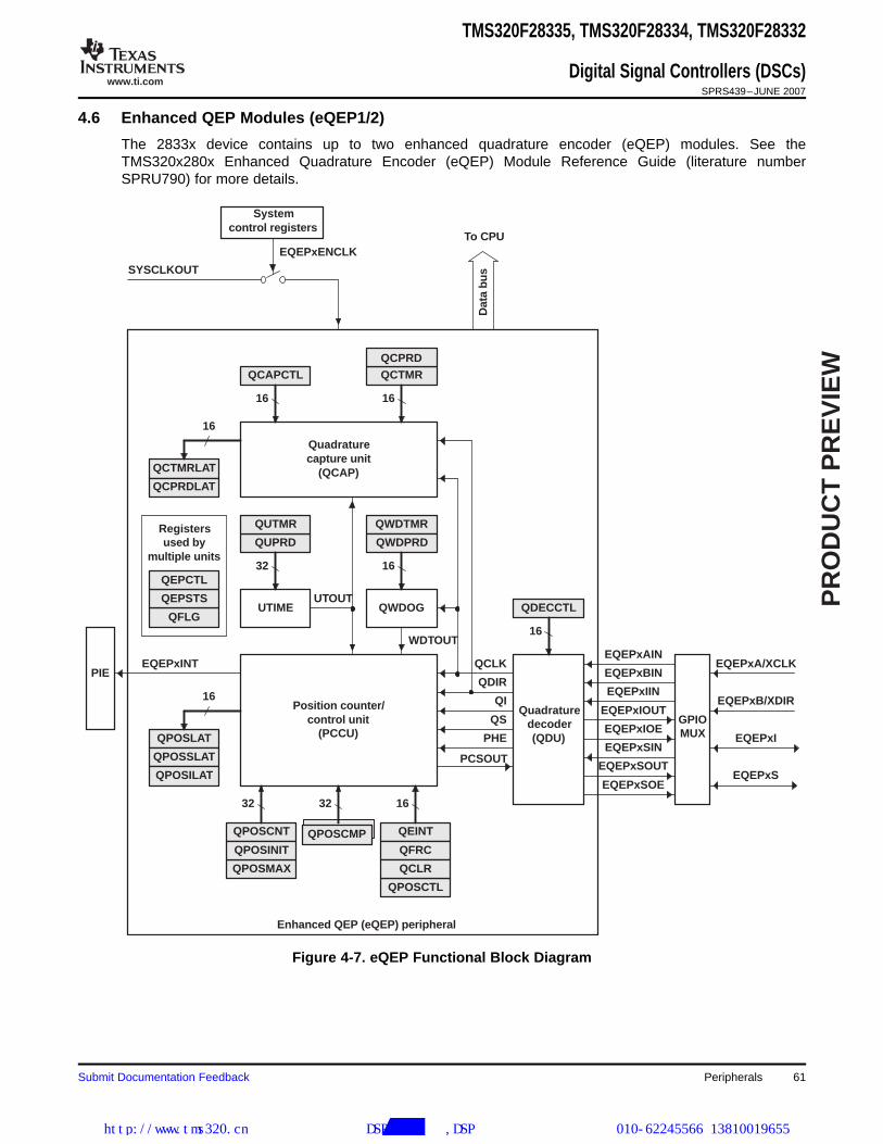
www.ti.com
PR
OD
UC
T P
RE
VIE
W
4.6 Enhanced QEP Modules (eQEP1/2)
QWDTMR
QWDPRD
16
QWDOGUTIME
QUPRD
QUTMR
32
UTOUT
WDTOUT
Quadraturecapture unit
(QCAP)QCPRDLAT
QCTMRLAT
16
QFLG
QEPSTS
QEPCTL
Registersused by
multiple units
QCLK
QDIR
QI
QS
PHE
PCSOUT
Quadraturedecoder(QDU)
QDECCTL
16
Position counter/control unit
(PCCU)QPOSLAT
QPOSSLAT
16
QPOSILAT
EQEPxAIN
EQEPxBIN
EQEPxIIN
EQEPxIOUT
EQEPxIOE
EQEPxSIN
EQEPxSOUT
EQEPxSOE
GPIOMUX
EQEPxA/XCLK
EQEPxB/XDIR
EQEPxS
EQEPxI
QPOSCMP QEINT
QFRC
32
QCLR
QPOSCTL
1632
QPOSCNT
QPOSMAX
QPOSINIT
PIEEQEPxINT
Enhanced QEP (eQEP) peripheral
Systemcontrol registers
QCTMRQCPRD
1616
QCAPCTL
EQEPxENCLK
SYSCLKOUT
Dat
a b
us
To CPU
TMS320F28335, TMS320F28334, TMS320F28332
Digital Signal Controllers (DSCs)SPRS439–JUNE 2007
The 2833x device contains up to two enhanced quadrature encoder (eQEP) modules. See theTMS320x280x Enhanced Quadrature Encoder (eQEP) Module Reference Guide (literature numberSPRU790) for more details.
Figure 4-7. eQEP Functional Block Diagram
Submit Documentation Feedback Peripherals 61
http://www.tms320.cn 提供DSP芯片解密,DSP破解等服务 010-62245566 13810019655

www.ti.com
PR
OD
UC
T P
RE
VIE
W
TMS320F28335, TMS320F28334, TMS320F28332
Digital Signal Controllers (DSCs)SPRS439–JUNE 2007
Table 4-4. eQEP Control and Status Registers
EQEP1EQEP1 EQEP2NAME SIZE(x16)/ REGISTER DESCRIPTIONADDRESS ADDRESS #SHADOW
QPOSCNT 0x6B00 0x6B40 2/0 eQEP Position Counter
QPOSINIT 0x6B02 0x6B42 2/0 eQEP Initialization Position Count
QPOSMAX 0x6B04 0x6B44 2/0 eQEP Maximum Position Count
QPOSCMP 0x6B06 0x6B46 2/1 eQEP Position-compare
QPOSILAT 0x6B08 0x6B48 2/0 eQEP Index Position Latch
QPOSSLAT 0x6B0A 0x6B4A 2/0 eQEP Strobe Position Latch
QPOSLAT 0x6B0C 0x6B4C 2/0 eQEP Position Latch
QUTMR 0x6B0E 0x6B4E 2/0 eQEP Unit Timer
QUPRD 0x6B10 0x6B50 2/0 eQEP Unit Period Register
QWDTMR 0x6B12 0x6B52 1/0 eQEP Watchdog Timer
QWDPRD 0x6B13 0x6B53 1/0 eQEP Watchdog Period Register
QDECCTL 0x6B14 0x6B54 1/0 eQEP Decoder Control Register
QEPCTL 0x6B15 0x6B55 1/0 eQEP Control Register
QCAPCTL 0x6B16 0x6B56 1/0 eQEP Capture Control Register
QPOSCTL 0x6B17 0x6B57 1/0 eQEP Position-compare Control Register
QEINT 0x6B18 0x6B58 1/0 eQEP Interrupt Enable Register
QFLG 0x6B19 0x6B59 1/0 eQEP Interrupt Flag Register
QCLR 0x6B1A 0x6B5A 1/0 eQEP Interrupt Clear Register
QFRC 0x6B1B 0x6B5B 1/0 eQEP Interrupt Force Register
QEPSTS 0x6B1C 0x6B5C 1/0 eQEP Status Register
QCTMR 0x6B1D 0x6B5D 1/0 eQEP Capture Timer
QCPRD 0x6B1E 0x6B5E 1/0 eQEP Capture Period Register
QCTMRLAT 0x6B1F 0x6B5F 1/0 eQEP Capture Timer Latch
QCPRDLAT 0x6B20 0x6B60 1/0 eQEP Capture Period Latch
Reserved 0x6B21- 0x6B61- 31/00x6B3F 0x6B7F
Peripherals62 Submit Documentation Feedback
http://www.tms320.cn 提供DSP芯片解密,DSP破解等服务 010-62245566 13810019655

www.ti.com
PR
OD
UC
T P
RE
VIE
W
4.7 Enhanced Analog-to-Digital Converter (ADC) Module
Digital Value 0,
Digital Value 4096 Input Analog Voltage ADCLO
3
when input ≤ 0 V
when 0 V < input < 3 V
when input ≥ 3 VDigital Value 4095,
TMS320F28335, TMS320F28334, TMS320F28332
Digital Signal Controllers (DSCs)SPRS439–JUNE 2007
A simplified functional block diagram of the ADC module is shown in Figure 4-8. The ADC moduleconsists of a 12-bit ADC with a built-in sample-and-hold (S/H) circuit. Functions of the ADC moduleinclude:• 12-bit ADC core with built-in S/H• Analog input: 0.0 V to 3.0 V (Voltages above 3.0 V produce full-scale conversion results.)• Fast conversion rate: Up to 80 ns at 25-MHz ADC clock, 12.5 MSPS• 16-channel, MUXed inputs• Autosequencing capability provides up to 16 "autoconversions" in a single session. Each conversion
can be programmed to select any 1 of 16 input channels• Sequencer can be operated as two independent 8-state sequencers or as one large 16-state
sequencer (i.e., two cascaded 8-state sequencers)• Sixteen result registers (individually addressable) to store conversion values
– The digital value of the input analog voltage is derived by:
A. All fractional values are truncated.
• Multiple triggers as sources for the start-of-conversion (SOC) sequence– S/W - software immediate start– ePWM start of conversion– XINT2 ADC start of conversion
• Flexible interrupt control allows interrupt request on every end-of-sequence (EOS) or every other EOS.• Sequencer can operate in "start/stop" mode, allowing multiple "time-sequenced triggers" to
synchronize conversions.• SOCA and SOCB triggers can operate independently in dual-sequencer mode.• Sample-and-hold (S/H) acquisition time window has separate prescale control.
The ADC module in the 2833x has been enhanced to provide flexible interface to ePWM peripherals. TheADC interface is built around a fast, 12-bit ADC module with a fast conversion rate of up to 80 ns at25-MHz ADC clock. The ADC module has 16 channels, configurable as two independent 8-channelmodules. The two independent 8-channel modules can be cascaded to form a 16-channel module.Although there are multiple input channels and two sequencers, there is only one converter in the ADCmodule. Figure 4-8 shows the block diagram of the ADC module.
The two 8-channel modules have the capability to autosequence a series of conversions, each modulehas the choice of selecting any one of the respective eight channels available through an analog MUX. Inthe cascaded mode, the autosequencer functions as a single 16-channel sequencer. On each sequencer,once the conversion is complete, the selected channel value is stored in its respective RESULT register.Autosequencing allows the system to convert the same channel multiple times, allowing the user toperform oversampling algorithms. This gives increased resolution over traditional single-sampledconversion results.
Submit Documentation Feedback Peripherals 63
http://www.tms320.cn 提供DSP芯片解密,DSP破解等服务 010-62245566 13810019655

www.ti.com
PR
OD
UC
T P
RE
VIE
W
Result Registers
EPWMSOCB
S/W
GPIO/XINT2_ADCSOC
EPWMSOCA
S/W
Sequencer 2Sequencer 1 SOCSOC
ADC Control Registers
70B7h
70B0h
70AFh
70A8h
Result Reg 15
Result Reg 8
Result Reg 7
Result Reg 1
Result Reg 0
ModuleADC12-Bit
AnalogMUX
ADCINA0
ADCINA7
ADCINB0
ADCINB7
SystemControl Block
High-SpeedPrescaler
HSPCLKADCENCLK
DSPSYSCLKOUT
S/H
S/H
HALT
TMS320F28335, TMS320F28334, TMS320F28332
Digital Signal Controllers (DSCs)SPRS439–JUNE 2007
Figure 4-8. Block Diagram of the ADC Module
To obtain the specified accuracy of the ADC, proper board layout is very critical. To the best extentpossible, traces leading to the ADCIN pins should not run in close proximity to the digital signal paths.This is to minimize switching noise on the digital lines from getting coupled to the ADC inputs.Furthermore, proper isolation techniques must be used to isolate the ADC module power pins ( VDD1A18,VDD2A18 , VDDA2, VDDAIO ) from the digital supply.Figure 4-9 shows the ADC pin connections for the 2833xdevices.
NOTE
1. The ADC registers are accessed at the SYSCLKOUT rate. The internal timing of theADC module is controlled by the high-speed peripheral clock (HSPCLK).
2. The behavior of the ADC module based on the state of the ADCENCLK and HALTsignals is as follows:
– ADCENCLK: On reset, this signal will be low. While reset is active-low (XRS) theclock to the register will still function. This is necessary to make sure all registersand modes go into their default reset state. The analog module, however, will bein a low-power inactive state. As soon as reset goes high, then the clock to theregisters will be disabled. When the user sets the ADCENCLK signal high, thenthe clocks to the registers will be enabled and the analog module will be enabled.There will be a certain time delay (ms range) before the ADC is stable and can beused.
– HALT: This mode only affects the analog module. It does not affect the registers.In this mode, the ADC module goes into low-power mode. This mode also will stopthe clock to the CPU, which will stop the HSPCLK; therefore, the ADC registerlogic will be turned off indirectly.
Peripherals64 Submit Documentation Feedback
http://www.tms320.cn 提供DSP芯片解密,DSP破解等服务 010-62245566 13810019655

www.ti.com
PR
OD
UC
T P
RE
VIE
W
ADCINA[7:0]ADCINB[7:0]
ADCLOADCREFIN
ADC External Current Bias Resistor ADCRESEXT
ADCREFP
VDD1A18VDD2A18
VSS1AGNDVSS2AGND
VDDAIOVSSAIO
VDDA2VSSA2
ADC Reference Positive Output
ADCREFMADC Reference Medium Output
ADC Power
ADC Analog and Reference I/O Power
Analog input 0−3 V with respect to ADCLO
Connect to analog ground
22 k
2.2 F (A)
2.2 F (A)
ADC Analog Power Pin (1.8 V)ADC Analog Power Pin (1.8 V)
ADC Analog Power Pin (3.3 V)ADC Analog I/O Ground Pin
ADC Analog Power Pin (3.3 V)
ADCREFP and ADCREFM should notbe loaded by external circuitry
ADC Analog Ground Pin
ADC 16-Channel Analog Inputs
Float or ground if internal reference is used
ADC Analog Ground PinADC Analog Ground Pin
ADCINA[7:0]ADCINB[7:0]
ADCLOADCREFIN
ADC External Current Bias Resistor ADCRESEXT
ADCREFP
VDD1A18VDD2A18
VSS1AGNDVSS2AGND
VDDAIOVSSAIO
VDDA2VSSA2
ADC Reference Positive Output
ADCREFMADC Reference Medium Output
ADC Analog Power
ADC Analog and Reference I/O Power
Analog input 0−3 V with respect to ADCLO
Connect to Analog Ground
22 k
2.2 F (A)
2.2 F (A) ADCREFP and ADCREFM should notbe loaded by external circuitry
ADC 16-Channel Analog Inputs
Connect to 1.500, 1.024, or 2.048-V precision source (D)
ADC Analog Power Pin (1.8 V)ADC Analog Power Pin (1.8 V)
ADC Analog I/O Ground Pin
ADC Analog Power Pin (3.3 V)ADC Analog Ground Pin
ADC Analog Ground PinADC Analog Ground Pin
ADC Analog Power Pin (3.3 V)
TMS320F28335, TMS320F28334, TMS320F28332
Digital Signal Controllers (DSCs)SPRS439–JUNE 2007
Figure 4-9 shows the ADC pin-biasing for internal reference and Figure 4-10 shows the ADC pin-biasingfor external reference.
A. TAIYO YUDEN LMK212BJ225MG-T or equivalent
B. External decoupling capacitors are recommended on all power pins.
C. Analog inputs must be driven from an operational amplifier that does not degrade the ADC performance.
Figure 4-9. ADC Pin Connections With Internal Reference
A. TAIYO YUDEN LMK212BJ225MG-T or equivalent
B. External decoupling capacitors are recommended on all power pins.
C. Analog inputs must be driven from an operational amplifier that does not degrade the ADC performance.
D. External voltage on ADCREFIN is enabled by changing bits 15:14 in the ADC Reference Select register depending onthe voltage used on this pin. TI recommends TI part REF3020 or equivalent for 2.048-V generation. Overall gainaccuracy will be determined by accuracy of this voltage source.
Figure 4-10. ADC Pin Connections With External Reference
Submit Documentation Feedback Peripherals 65
http://www.tms320.cn 提供DSP芯片解密,DSP破解等服务 010-62245566 13810019655

www.ti.com
PR
OD
UC
T P
RE
VIE
W
4.7.1 ADC Connections if the ADC Is Not Used
4.7.2 ADC Registers
TMS320F28335, TMS320F28334, TMS320F28332
Digital Signal Controllers (DSCs)SPRS439–JUNE 2007
NOTEThe temperature rating of any recommended component must match the rating of the endproduct.
It is recommended to keep the connections for the analog power pins, even if the ADC is not used.Following is a summary of how the ADC pins should be connected, if the ADC is not used in anapplication:• VDD1A18/VDD2A18 – Connect to VDD
• VDDA2, VDDAIO – Connect to VDDIO
• VSS1AGND/VSS2AGND, VSSA2, VSSAIO – Connect to VSS
• ADCLO – Connect to VSS
• ADCREFIN – Connect to VSS
• ADCREFP/ADCREFM – Connect a 100-nF cap to VSS
• ADCRESEXT – Connect a 20-kΩ resistor (very loose tolerance) to VSS.• ADCINAn, ADCINBn - Connect to VSS
When the ADC is not used, be sure that the clock to the ADC module is not turned on to realize powersavings.
When the ADC module is used in an application, unused ADC input pins should be connected to analogground (VSS1AGND/VSS2AGND)
The ADC operation is configured, controlled, and monitored by the registers listed in Table 4-5.
Table 4-5. ADC Registers (1)
NAME ADDRESS (1) ADDRESS (2) SIZE (x16) DESCRIPTION
ADCTRL1 0x7100 1 ADC Control Register 1
ADCTRL2 0x7101 1 ADC Control Register 2
ADCMAXCONV 0x7102 1 ADC Maximum Conversion Channels Register
ADCCHSELSEQ1 0x7103 1 ADC Channel Select Sequencing Control Register 1
ADCCHSELSEQ2 0x7104 1 ADC Channel Select Sequencing Control Register 2
ADCCHSELSEQ3 0x7105 1 ADC Channel Select Sequencing Control Register 3
ADCCHSELSEQ4 0x7106 1 ADC Channel Select Sequencing Control Register 4
ADCASEQSR 0x7107 1 ADC Auto-Sequence Status Register
ADCRESULT0 0x7108 0x0B00 1 ADC Conversion Result Buffer Register 0
ADCRESULT1 0x7109 0x0B01 1 ADC Conversion Result Buffer Register 1
ADCRESULT2 0x710A 0x0B02 1 ADC Conversion Result Buffer Register 2
ADCRESULT3 0x710B 0x0B03 1 ADC Conversion Result Buffer Register 3
ADCRESULT4 0x710C 0x0B04 1 ADC Conversion Result Buffer Register 4
ADCRESULT5 0x710D 0x0B05 1 ADC Conversion Result Buffer Register 5
ADCRESULT6 0x710E 0x0B06 1 ADC Conversion Result Buffer Register 6
ADCRESULT7 0x710F 0x0B07 1 ADC Conversion Result Buffer Register 7
ADCRESULT8 0x7110 0x0B08 1 ADC Conversion Result Buffer Register 8
ADCRESULT9 0x7111 0x0B09 1 ADC Conversion Result Buffer Register 9
(1) The registers in this column are Peripheral Frame 2 Registers.(2) The ADC result registers are dual mapped in the 2833x DSC. Locations in Peripheral Frame 2 (0x7108-0x7117) are 2 wait-states and
left justified. Locations in Peripheral frame 0 space (0x0B00-0x0B0F) are 0 wait sates and right justified. During high speed/continuousconversion use of the ADC, use the 0 wait-state locations for fast transfer of ADC results to user memory.
Peripherals66 Submit Documentation Feedback
http://www.tms320.cn 提供DSP芯片解密,DSP破解等服务 010-62245566 13810019655

www.ti.com
PR
OD
UC
T P
RE
VIE
W
TMS320F28335, TMS320F28334, TMS320F28332
Digital Signal Controllers (DSCs)SPRS439–JUNE 2007
Table 4-5. ADC Registers (continued)
NAME ADDRESS (1) ADDRESS (2) SIZE (x16) DESCRIPTION
ADCRESULT10 0x7112 0x0B0A 1 ADC Conversion Result Buffer Register 10
ADCRESULT11 0x7113 0x0B0B 1 ADC Conversion Result Buffer Register 11
ADCRESULT12 0x7114 0x0B0C 1 ADC Conversion Result Buffer Register 12
ADCRESULT13 0x7115 0x0B0D 1 ADC Conversion Result Buffer Register 13
ADCRESULT14 0x7116 0x0B0E 1 ADC Conversion Result Buffer Register 14
ADCRESULT15 0x7117 0x0B0F 1 ADC Conversion Result Buffer Register 15
ADCTRL3 0x7118 1 ADC Control Register 3
ADCST 0x7119 1 ADC Status Register
0x711AReserved 20x711B
ADCREFSEL 0x711C 1 ADC Reference Select Register
ADCOFFTRIM 0x711D 1 ADC Offset Trim Register
0x711EReserved 2 ADC Status Register0x711F
Submit Documentation Feedback Peripherals 67
http://www.tms320.cn 提供DSP芯片解密,DSP破解等服务 010-62245566 13810019655

www.ti.com
PR
OD
UC
T P
RE
VIE
W
4.8 Multichannel Buffered Serial Port (McBSP) Module
• McBSP clock rate = ( )CLKSRG
CLKG =1+ CLKGDIV where CLKSRG source could be LSPCLK, CLKX, or CLKR.
TMS320F28335, TMS320F28334, TMS320F28332
Digital Signal Controllers (DSCs)SPRS439–JUNE 2007
The McBSP module has the following features:• Compatible to McBSP in TMS320C54x™ /TMS320C55x™ DSC devices, except the DMA features• Full–duplex communication• Double–buffered data registers that allow a continuous data stream• Independent framing and clocking for receive and transmit• External shift clock generation or an internal programmable frequency shift clock• A wide selection of data sizes including 8–, 12–, 16–, 20–, 24–, or 32–bits• 8–bit data transfers with LSB or MSB first• Programmable polarity for both frame synchronization and data clocks• HIghly programmable internal clock and frame generation• Support A–bis mode• Direct interface to industry–standard CODECs, Analog Interface Chips (AICs), and other serially
connected A/D and D/A devices• Works with SPI–compatible devices
The following application interfaces can be supported on the McBSP:• T1/E1 framers• MVIP switching–compatible and ST–BUS–compliant devices including:
– MVIP framers– H.100 framers– SCSA framers– IOM–2 compliant devices– AC97–compliant devices (the necessary multiphase frame synchronization capability is provided.)– IIS–compliant devices
Serial port performance is limited by I/O buffer switching speed. Internal prescalers must be adjustedsuch that the peripheral speed is less than the I/O buffer speed limit—20–MHz maximum.
Figure 4-11 shows the block diagram of the McBSP module.
Peripherals68 Submit Documentation Feedback
http://www.tms320.cn 提供DSP芯片解密,DSP破解等服务 010-62245566 13810019655
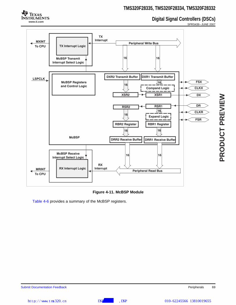
www.ti.com
PR
OD
UC
T P
RE
VIE
W
McBSP Receive
Interrupt Select Logic
DX
DR
Expand Logic
DRR1 Receive Buffer
RXInterrupt
DRR2 Receive Buffer
RBR1 RegisterRBR2 Register
McBSP Registers
and Control LogicCLKX
FSX
CLKR
FSR
16
Compand Logic
DXR2 Transmit Buffer
RSR1
XSR2 XSR1
Peripheral Read Bus
16
1616
1616
RSR2
DXR1 Transmit BufferLSPCLK
MRINT
To CPU
McBSP
RX Interrupt Logic
McBSP Transmit
Interrupt Select Logic
TXInterruptMXINT
To CPU TX Interrupt LogicPeripheral Write Bus
16 16
16 16
TMS320F28335, TMS320F28334, TMS320F28332
Digital Signal Controllers (DSCs)SPRS439–JUNE 2007
Figure 4-11. McBSP Module
Table 4-6 provides a summary of the McBSP registers.
Submit Documentation Feedback Peripherals 69
http://www.tms320.cn 提供DSP芯片解密,DSP破解等服务 010-62245566 13810019655

www.ti.com
PR
OD
UC
T P
RE
VIE
W
TMS320F28335, TMS320F28334, TMS320F28332
Digital Signal Controllers (DSCs)SPRS439–JUNE 2007
Table 4-6. McBSP Register Summary
NAME McBSP-A McBSP-B TYPE RESET VALUE DESCRIPTIONADDRESS ADDRESS
DATA REGISTERS, RECEIVE, TRANSMIT
DRR2 0x5000 0x5040 R 0x0000 McBSP Data Receive Register 2
DRR1 0x5001 0x5041 R 0x0000 McBSP Data Receive Register 1
DXR2 0x5002 0x5042 W 0x0000 McBSP Data Transmit Register 2
DXR1 0x5003 0x5043 W 0x0000 McBSP Data Transmit Register 1
McBSP CONTROL REGISTERS
SPCR2 0x5004 0x5044 R/W 0x0000 McBSP Serial Port Control Register 2
SPCR1 0x5005 0x5045 R/W 0x0000 McBSP Serial Port Control Register 1
RCR2 0x5006 0x5046 R/W 0x0000 McBSP Receive Control Register 2
RCR1 0x5007 0x5047 R/W 0x0000 McBSP Receive Control Register 1
XCR2 0x5008 0x5048 R/W 0x0000 McBSP Transmit Control Register 2
XCR1 0x5009 0x5049 R/W 0x0000 McBSP Transmit Control Register 1
SRGR2 0x500A 0x504A R/W 0x0000 McBSP Sample Rate Generator Register 2
SRGR1 0x500B 0x504B R/W 0x0000 McBSP Sample Rate Generator Register 1
MULTICHANNEL CONTROL REGISTERS
MCR2 0x500C 0x504C R/W 0x0000 McBSP Multichannel Register 2
MCR1 0x500D 0x504D R/W 0x0000 McBSP Multichannel Register 1
RCERA 0x500E 0x504E R/W 0x0000 McBSP Receive Channel Enable Register Partition A
RCERB 0x500F 0x504F R/W 0x0000 McBSP Receive Channel Enable Register Partition B
XCERA 0x5010 0x5050 R/W 0x0000 McBSP Transmit Channel Enable Register Partition A
XCERB 0x5011 0x5051 R/W 0x0000 McBSP Transmit Channel Enable Register Partition B
PCR 0x5012 0x5052 R/W 0x0000 McBSP Pin Control Register
RCERC 0x5013 0x5053 R/W 0x0000 McBSP Receive Channel Enable Register Partition C
RCERD 0x5014 0x5054 R/W 0x0000 McBSP Receive Channel Enable Register Partition D
XCERC 0x5015 0x5055 R/W 0x0000 McBSP Transmit Channel Enable Register Partition C
XCERD 0x5016 0x5056 R/W 0x0000 McBSP Transmit Channel Enable Register Partition D
RCERE 0x5017 0x5057 R/W 0x0000 McBSP Receive Channel Enable Register Partition E
RCERF 0x5018 0x5058 R/W 0x0000 McBSP Receive Channel Enable Register Partition F
XCERE 0x5019 0x5059 R/W 0x0000 McBSP Transmit Channel Enable Register Partition E
XCERF 0x501A 0x505A R/W 0x0000 McBSP Transmit Channel Enable Register Partition F
RCERG 0x501B 0x505B R/W 0x0000 McBSP Receive Channel Enable Register Partition G
RCERH 0x501C 0x505C R/W 0x0000 McBSP Receive Channel Enable Register Partition H
XCERG 0x501D 0x505D R/W 0x0000 McBSP Transmit Channel Enable Register Partition G
XCERH 0x501E 0x505E R/W 0x0000 McBSP Transmit Channel Enable Register Partition H
MFFINT 0x5023 0x5063 R/W 0x0000 McBSP Interrupt Enable Register
MFFST 0x5024 0x5064 R/W 0x0000 McBSP Pin Status Register
Peripherals70 Submit Documentation Feedback
http://www.tms320.cn 提供DSP芯片解密,DSP破解等服务 010-62245566 13810019655

www.ti.com
PR
OD
UC
T P
RE
VIE
W
4.9 Enhanced Controller Area Network (eCAN) Modules (eCAN-A and eCAN-B)
TMS320F28335, TMS320F28334, TMS320F28332
Digital Signal Controllers (DSCs)SPRS439–JUNE 2007
The CAN module has the following features:• Fully compliant with CAN protocol, version 2.0B• Supports data rates up to 1 Mbps• Thirty-two mailboxes, each with the following properties:
– Configurable as receive or transmit– Configurable with standard or extended identifier– Has a programmable receive mask– Supports data and remote frame– Composed of 0 to 8 bytes of data– Uses a 32-bit time stamp on receive and transmit message– Protects against reception of new message– Holds the dynamically programmable priority of transmit message– Employs a programmable interrupt scheme with two interrupt levels– Employs a programmable alarm on transmission or reception time-out
• Low-power mode• Programmable wake-up on bus activity• Automatic reply to a remote request message• Automatic retransmission of a frame in case of loss of arbitration or error• 32-bit local network time counter synchronized by a specific message (communication in conjunction
with mailbox 16)• Self-test mode
– Operates in a loopback mode receiving its own message. A "dummy" acknowledge is provided,thereby eliminating the need for another node to provide the acknowledge bit.
NOTEFor a SYSCLKOUT of 100 MHz, the smallest bit rate possible is 15.625 kbps.
For a SYSCLKOUT of 150 MHz, the smallest bit rate possible is 23.4 kbps.
Submit Documentation Feedback Peripherals 71
http://www.tms320.cn 提供DSP芯片解密,DSP破解等服务 010-62245566 13810019655

www.ti.com
PR
OD
UC
T P
RE
VIE
W
Mailbox RAM(512 Bytes)
32-Message Mailboxof 4 × 32-Bit Words
Memory ManagementUnit
CPU Interface,Receive Control Unit,
Timer Management Unit
eCAN Memory(512 Bytes)
Registers and MessageObjects Control32 32
Message Controller
32 3232 3232 32
eCAN Protocol Kernel Receive Buffer
Transmit Buffer
Control Buffer
Status Buffer
Enhanced CAN Controller32
Controls Address DataeCAN1INTeCAN0INT
32
SN65HVD23x3.3-V CAN Transceiver
CAN Bus
TMS320F28335, TMS320F28334, TMS320F28332
Digital Signal Controllers (DSCs)SPRS439–JUNE 2007
Figure 4-12. eCAN Block Diagram and Interface Circuit
Table 4-7. 3.3-V eCAN Transceivers
SUPPLY LOW-POWER SLOPEPART NUMBER VREF OTHER TAVOLTAGE MODE CONTROL
SN65HVD230 3.3 V Standby Adjustable Yes – -40°C to 85°C
SN65HVD230Q 3.3 V Standby Adjustable Yes – -40°C to 125°C
SN65HVD231 3.3 V Sleep Adjustable Yes – -40°C to 85°C
SN65HVD231Q 3.3 V Sleep Adjustable Yes – -40°C to 125°C
SN65HVD232 3.3 V None None None – -40°C to 85°C
SN65HVD232Q 3.3 V None None None – -40°C to 125°C
SN65HVD233 3.3 V Standby Adjustable None Diagnostic -40°C to 125°CLoopback
SN65HVD234 3.3 V Standby and Sleep Adjustable None – -40°C to 125°C
SN65HVD235 3.3 V Standby Adjustable None Autobaud -40°C to 125°CLoopback
Peripherals72 Submit Documentation Feedback
http://www.tms320.cn 提供DSP芯片解密,DSP破解等服务 010-62245566 13810019655

www.ti.com
PR
OD
UC
T P
RE
VIE
W
Mailbox Enable − CANME
Mailbox Direction − CANMD
Transmission Request Set − CANTRS
Transmission Request Reset − CANTRR
Transmission Acknowledge − CANT A
Abort Acknowledge − CANAA
Received Message Pending − CANRMP
Received Message Lost − CANRML
Remote Frame Pending − CANRFP
Global Acceptance Mask − CANGAM
Master Control − CANMC
Bit-T iming Configuration − CANBTC
Error and Status − CANES
Transmit Error Counter − CANTEC
Receive Error Counter − CANREC
Global Interrupt Flag 0 − CANGIF0
Global Interrupt Mask − CANGIM
Mailbox Interrupt Mask − CANMIM
Mailbox Interrupt Level − CANMIL
Overwrite Protection Control − CANOPC
TX I/O Control − CANTIOC
RX I/O Control − CANRIOC
Time Stamp Counter − CANTSC
Global Interrupt Flag 1 − CANGIF1
Time-Out Control − CANT OC
Time-Out Status − CANT OS
Reserved
eCAN-A Control and Status Registers
Message Identifier − MSGID61E8h−61E9h
Message Control − MSGCTRL
Message Data Low − MDL
Message Data High − MDH
Message Mailbox (16 Bytes)
Control and Status Registers6000h
603Fh
Local Acceptance Masks (LAM)(32 × 32-Bit RAM)
6040h
607Fh
6080h
60BFh
60C0h
60FFh
eCAN-A Memory (512 Bytes)
Message Object T ime Stamps (MOTS)(32 × 32-Bit RAM)
Message Object T ime-Out (MOT O)(32 × 32-Bit RAM)
Mailbox 06100h−6107h
Mailbox 16108h−610Fh
Mailbox 26110h−6117h
Mailbox 36118h−611Fh
eCAN-A Memory RAM (512 Bytes)
Mailbox 46120h−6127h
Mailbox 2861E0h−61E7h
Mailbox 2961E8h−61EFh
Mailbox 3061F0h−61F7h
Mailbox 3161F8h−61FFh
61EAh−61EBh
61ECh−61EDh
61EEh−61EFh
TMS320F28335, TMS320F28334, TMS320F28332
Digital Signal Controllers (DSCs)SPRS439–JUNE 2007
Figure 4-13. eCAN-A Memory Map
Submit Documentation Feedback Peripherals 73
http://www.tms320.cn 提供DSP芯片解密,DSP破解等服务 010-62245566 13810019655

www.ti.com
PR
OD
UC
T P
RE
VIE
W
Mailbox Enable − CANME
Mailbox Direction − CANMD
Transmission Request Set − CANTRS
Transmission Request Reset − CANTRR
Transmission Acknowledge − CANT A
Abort Acknowledge − CANAA
Received Message Pending − CANRMP
Received Message Lost − CANRML
Remote Frame Pending − CANRFP
Global Acceptance Mask − CANGAM
Master Control − CANMC
Bit-T iming Configuration − CANBTC
Error and Status − CANES
Transmit Error Counter − CANTEC
Receive Error Counter − CANREC
Global Interrupt Flag 0 − CANGIF0
Global Interrupt Mask − CANGIM
Mailbox Interrupt Mask − CANMIM
Mailbox Interrupt Level − CANMIL
Overwrite Protection Control − CANOPC
TX I/O Control − CANTIOC
RX I/O Control − CANRIOC
Time Stamp Counter − CANTSC
Global Interrupt Flag 1 − CANGIF1
Time-Out Control − CANT OC
Time-Out Status − CANT OS
Reserved
eCAN-B Control and Status Registers
Message Identifier − MSGID63E8h−63E9h
Message Control − MSGCTRL
Message Data Low − MDL
Message Data High − MDH
Message Mailbox (16 Bytes)
Control and Status Registers6200h
623Fh
Local Acceptance Masks (LAM)(32 × 32-Bit RAM)
6240h
627Fh
6280h
62BFh
62C0h
62FFh
eCAN-B Memory (512 Bytes)
Message Object T ime Stamps (MOTS)(32 × 32-Bit RAM)
Message Object T ime-Out (MOT O)(32 × 32-Bit RAM)
Mailbox 06300h−6307h
Mailbox 16308h−630Fh
Mailbox 26310h−6317h
Mailbox 36318h−631Fh
eCAN-B Memory RAM (512 Bytes)
Mailbox 46320h−6327h
Mailbox 2863E0h−63E7h
Mailbox 2963E8h−63EFh
Mailbox 3063F0h−63F7h
Mailbox 3163F8h−63FFh
63EAh−63EBh
63ECh−63EDh
63EEh−63EFh
TMS320F28335, TMS320F28334, TMS320F28332
Digital Signal Controllers (DSCs)SPRS439–JUNE 2007
Figure 4-14. eCAN-B Memory Map
The CAN registers listed in Table 4-8 are used by the CPU to configure and control the CAN controllerand the message objects. eCAN control registers only support 32-bit read/write operations. Mailbox RAMcan be accessed as 16 bits or 32 bits. 32-bit accesses are aligned to an even boundary.
Peripherals74 Submit Documentation Feedback
http://www.tms320.cn 提供DSP芯片解密,DSP破解等服务 010-62245566 13810019655

www.ti.com
PR
OD
UC
T P
RE
VIE
W
TMS320F28335, TMS320F28334, TMS320F28332
Digital Signal Controllers (DSCs)SPRS439–JUNE 2007
Table 4-8. CAN Register Map (1)
ECAN-A ECAN-B SIZEREGISTER NAME DESCRIPTIONADDRESS ADDRESS (x32)
CANME 0x6000 0x6200 1 Mailbox enable
CANMD 0x6002 0x6202 1 Mailbox direction
CANTRS 0x6004 0x6204 1 Transmit request set
CANTRR 0x6006 0x6206 1 Transmit request reset
CANTA 0x6008 0x6208 1 Transmission acknowledge
CANAA 0x600A 0x620A 1 Abort acknowledge
CANRMP 0x600C 0x620C 1 Receive message pending
CANRML 0x600E 0x620E 1 Receive message lost
CANRFP 0x6010 0x6210 1 Remote frame pending
CANGAM 0x6012 0x6212 1 Global acceptance mask
CANMC 0x6014 0x6214 1 Master control
CANBTC 0x6016 0x6216 1 Bit-timing configuration
CANES 0x6018 0x6218 1 Error and status
CANTEC 0x601A 0x621A 1 Transmit error counter
CANREC 0x601C 0x621C 1 Receive error counter
CANGIF0 0x601E 0x621E 1 Global interrupt flag 0
CANGIM 0x6020 0x6220 1 Global interrupt mask
CANGIF1 0x6022 0x6222 1 Global interrupt flag 1
CANMIM 0x6024 0x6224 1 Mailbox interrupt mask
CANMIL 0x6026 0x6226 1 Mailbox interrupt level
CANOPC 0x6028 0x6228 1 Overwrite protection control
CANTIOC 0x602A 0x622A 1 TX I/O control
CANRIOC 0x602C 0x622C 1 RX I/O control
CANTSC 0x602E 0x622E 1 Time stamp counter (Reserved in SCC mode)
CANTOC 0x6030 0x6230 1 Time-out control (Reserved in SCC mode)
CANTOS 0x6032 0x6232 1 Time-out status (Reserved in SCC mode)
(1) These registers are mapped to Peripheral Frame 1.
Submit Documentation Feedback Peripherals 75
http://www.tms320.cn 提供DSP芯片解密,DSP破解等服务 010-62245566 13810019655

www.ti.com
PR
OD
UC
T P
RE
VIE
W
4.10 Serial Communications Interface (SCI) Modules (SCI-A, SCI-B, SCI-C)
Baud rate =
LSPCLK16
LSPCLK(BRR 1) * 8 when BRR ≠ 0
Baud rate = when BRR = 0
•Max bit rate 150 MHz
16 9.375 106 bs
(for 150-MHz devices)
•Max bit rate 100 MHz
16 6.25 106 bs
(for 100-MHz devices)
TMS320F28335, TMS320F28334, TMS320F28332
Digital Signal Controllers (DSCs)SPRS439–JUNE 2007
The 2833x devices include three serial communications interface (SCI) modules. The SCI modulessupport digital communications between the CPU and other asynchronous peripherals that use thestandard non-return-to-zero (NRZ) format. The SCI receiver and transmitter are double-buffered, and eachhas its own separate enable and interrupt bits. Both can be operated independently or simultaneously inthe full-duplex mode. To ensure data integrity, the SCI checks received data for break detection, parity,overrun, and framing errors. The bit rate is programmable to over 65000 different speeds through a 16-bitbaud-select register.
Features of each SCI module include:• Two external pins:
– SCITXD: SCI transmit-output pin– SCIRXD: SCI receive-input pin
NOTE: Both pins can be used as GPIO if not used for SCI.– Baud rate programmable to 64K different rates:
• Data-word format– One start bit– Data-word length programmable from one to eight bits– Optional even/odd/no parity bit– One or two stop bits
• Four error-detection flags: parity, overrun, framing, and break detection• Two wake-up multiprocessor modes: idle-line and address bit• Half- or full-duplex operation• Double-buffered receive and transmit functions• Transmitter and receiver operations can be accomplished through interrupt-driven or polled algorithms
with status flags.– Transmitter: TXRDY flag (transmitter-buffer register is ready to receive another character) and TX
EMPTY flag (transmitter-shift register is empty)– Receiver: RXRDY flag (receiver-buffer register is ready to receive another character), BRKDT flag
(break condition occurred), and RX ERROR flag (monitoring four interrupt conditions)• Separate enable bits for transmitter and receiver interrupts (except BRKDT)
• NRZ (non-return-to-zero) format• Ten SCI module control registers located in the control register frame beginning at address 7050h
NOTEAll registers in this module are 8-bit registers that are connected to Peripheral Frame 2.When a register is accessed, the register data is in the lower byte (7-0), and the upperbyte (15-8) is read as zeros. Writing to the upper byte has no effect.
Enhanced features:• Auto baud-detect hardware logic
Peripherals76 Submit Documentation Feedback
http://www.tms320.cn 提供DSP芯片解密,DSP破解等服务 010-62245566 13810019655
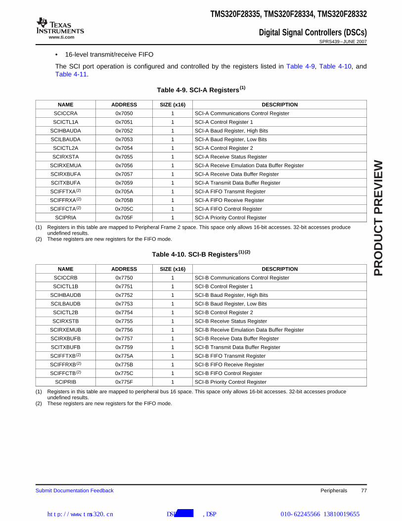
www.ti.com
PR
OD
UC
T P
RE
VIE
W
TMS320F28335, TMS320F28334, TMS320F28332
Digital Signal Controllers (DSCs)SPRS439–JUNE 2007
• 16-level transmit/receive FIFO
The SCI port operation is configured and controlled by the registers listed in Table 4-9, Table 4-10, andTable 4-11.
Table 4-9. SCI-A Registers (1)
NAME ADDRESS SIZE (x16) DESCRIPTION
SCICCRA 0x7050 1 SCI-A Communications Control Register
SCICTL1A 0x7051 1 SCI-A Control Register 1
SCIHBAUDA 0x7052 1 SCI-A Baud Register, High Bits
SCILBAUDA 0x7053 1 SCI-A Baud Register, Low Bits
SCICTL2A 0x7054 1 SCI-A Control Register 2
SCIRXSTA 0x7055 1 SCI-A Receive Status Register
SCIRXEMUA 0x7056 1 SCI-A Receive Emulation Data Buffer Register
SCIRXBUFA 0x7057 1 SCI-A Receive Data Buffer Register
SCITXBUFA 0x7059 1 SCI-A Transmit Data Buffer Register
SCIFFTXA (2) 0x705A 1 SCI-A FIFO Transmit Register
SCIFFRXA (2) 0x705B 1 SCI-A FIFO Receive Register
SCIFFCTA (2) 0x705C 1 SCI-A FIFO Control Register
SCIPRIA 0x705F 1 SCI-A Priority Control Register
(1) Registers in this table are mapped to Peripheral Frame 2 space. This space only allows 16-bit accesses. 32-bit accesses produceundefined results.
(2) These registers are new registers for the FIFO mode.
Table 4-10. SCI-B Registers (1) (2)
NAME ADDRESS SIZE (x16) DESCRIPTION
SCICCRB 0x7750 1 SCI-B Communications Control Register
SCICTL1B 0x7751 1 SCI-B Control Register 1
SCIHBAUDB 0x7752 1 SCI-B Baud Register, High Bits
SCILBAUDB 0x7753 1 SCI-B Baud Register, Low Bits
SCICTL2B 0x7754 1 SCI-B Control Register 2
SCIRXSTB 0x7755 1 SCI-B Receive Status Register
SCIRXEMUB 0x7756 1 SCI-B Receive Emulation Data Buffer Register
SCIRXBUFB 0x7757 1 SCI-B Receive Data Buffer Register
SCITXBUFB 0x7759 1 SCI-B Transmit Data Buffer Register
SCIFFTXB (2) 0x775A 1 SCI-B FIFO Transmit Register
SCIFFRXB (2) 0x775B 1 SCI-B FIFO Receive Register
SCIFFCTB (2) 0x775C 1 SCI-B FIFO Control Register
SCIPRIB 0x775F 1 SCI-B Priority Control Register
(1) Registers in this table are mapped to peripheral bus 16 space. This space only allows 16-bit accesses. 32-bit accesses produceundefined results.
(2) These registers are new registers for the FIFO mode.
Submit Documentation Feedback Peripherals 77
http://www.tms320.cn 提供DSP芯片解密,DSP破解等服务 010-62245566 13810019655

www.ti.com
PR
OD
UC
T P
RE
VIE
W
TMS320F28335, TMS320F28334, TMS320F28332
Digital Signal Controllers (DSCs)SPRS439–JUNE 2007
Table 4-11. SCI-C Registers (1) (2)
NAME ADDRESS SIZE (x16) DESCRIPTION
SCICCRC 0x7770 1 SCI-C Communications Control Register
SCICTL1C 0x7771 1 SCI-C Control Register 1
SCIHBAUDC 0x7772 1 SCI-C Baud Register, High Bits
SCILBAUDC 0x7773 1 SCI-C Baud Register, Low Bits
SCICTL2C 0x7774 1 SCI-C Control Register 2
SCIRXSTC 0x7775 1 SCI-C Receive Status Register
SCIRXEMUC 0x7776 1 SCI-C Receive Emulation Data Buffer Register
SCIRXBUFC 0x7777 1 SCI-C Receive Data Buffer Register
SCITXBUFC 0x7779 1 SCI-C Transmit Data Buffer Register
SCIFFTXC (2) 0x777A 1 SCI-C FIFO Transmit Register
SCIFFRXC (2) 0x777B 1 SCI-C FIFO Receive Register
SCIFFCTC (2) 0x777C 1 SCI-C FIFO Control Register
SCIPRC 0x777F 1 SCI-C Priority Control Register
(1) Registers in this table are mapped to peripheral bus 16 space. This space only allows 16-bit accesses. 32-bit accesses produceundefined results.
(2) These registers are new registers for the FIFO mode.
Peripherals78 Submit Documentation Feedback
http://www.tms320.cn 提供DSP芯片解密,DSP破解等服务 010-62245566 13810019655
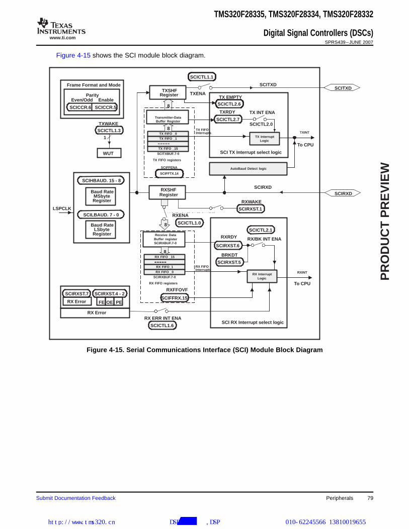
www.ti.com
PR
OD
UC
T P
RE
VIE
W
TX FIFO _0
LSPCLK
WUT
Frame Format and Mode
Even/Odd EnableParity
SCI RX Interrupt select logic
BRKDT
RXRDY
SCIRXST.6
SCICTL1.3
8SCICTL2.1
RX/BK INT ENA
SCIRXD
SCIRXST.1
TXENA
SCI TX Interrupt select logic
TX EMPTY
TXRDY
SCICTL2.0
TX INT ENA
SCITXD
RXENA
SCIRXD
RXWAKE
SCICTL1.6
RX ERR INT ENA
TXWAKE
SCITXD
SCICCR.6 SCICCR.5
SCITXBUF.7-0
SCIHBAUD. 15 - 8
Baud RateMSbyteRegister
SCILBAUD. 7 - 0
Transmitter-DataBuffer Register
8 SCICTL2.6
SCICTL2.7
Baud RateLSbyte
Register
RXSHFRegister
TXSHFRegister
SCIRXST.5
1 TX FIFO _1
-----TX FIFO _15
8
TX FIFO registers
TX FIFO
TX InterruptLogic
TXINT
SCIFFTX.14
RX FIFO _15
SCIRXBUF.7-0
Receive DataBuffer registerSCIRXBUF.7-0
-----RX FIFO_1
RX FIFO _0
8
RX FIFO registers
SCICTL1.0
RX InterruptLogic
RXINT
RX FIFO
SCIFFRX.15
RXFFOVF
RX Error
SCIRXST.7
PEFE OERX Error
SCIRXST.4 - 2
To CPU
To CPU
AutoBaud Detect logic
SCICTL1.1
SCIFFENA
Interrupts
Interrupts
TMS320F28335, TMS320F28334, TMS320F28332
Digital Signal Controllers (DSCs)SPRS439–JUNE 2007
Figure 4-15 shows the SCI module block diagram.
Figure 4-15. Serial Communications Interface (SCI) Module Block Diagram
Submit Documentation Feedback Peripherals 79
http://www.tms320.cn 提供DSP芯片解密,DSP破解等服务 010-62245566 13810019655

www.ti.com
PR
OD
UC
T P
RE
VIE
W
4.11 Serial Peripheral Interface (SPI) Module (SPI-A)
Baud rate =
LSPCLK4
LSPCLK(SPIBRR 1) when SPIBRR = 3 to 127
Baud rate = when SPIBRR = 0,1, 2
TMS320F28335, TMS320F28334, TMS320F28332
Digital Signal Controllers (DSCs)SPRS439–JUNE 2007
The 2833x devices include the four-pin serial peripheral interface (SPI) module. One SPI module (SPI-A)is available. The SPI is a high-speed, synchronous serial I/O port that allows a serial bit stream ofprogrammed length (one to sixteen bits) to be shifted into and out of the device at a programmablebit-transfer rate. Normally, the SPI is used for communications between the DSC controller and externalperipherals or another processor. Typical applications include external I/O or peripheral expansion throughdevices such as shift registers, display drivers, and ADCs. Multidevice communications are supported bythe master/slave operation of the SPI.
The SPI module features include:• Four external pins:
– SPISOMI: SPI slave-output/master-input pin– SPISIMO: SPI slave-input/master-output pin– SPISTE: SPI slave transmit-enable pin– SPICLK: SPI serial-clock pin
NOTE: All four pins can be used as GPIO, if the SPI module is not used.• Two operational modes: master and slave
Baud rate: 125 different programmable rates.
• Data word length: one to sixteen data bits• Four clocking schemes (controlled by clock polarity and clock phase bits) include:
– Falling edge without phase delay: SPICLK active-high. SPI transmits data on the falling edge of theSPICLK signal and receives data on the rising edge of the SPICLK signal.
– Falling edge with phase delay: SPICLK active-high. SPI transmits data one half-cycle ahead of thefalling edge of the SPICLK signal and receives data on the falling edge of the SPICLK signal.
– Rising edge without phase delay: SPICLK inactive-low. SPI transmits data on the rising edge of theSPICLK signal and receives data on the falling edge of the SPICLK signal.
– Rising edge with phase delay: SPICLK inactive-low. SPI transmits data one half-cycle ahead of thefalling edge of the SPICLK signal and receives data on the rising edge of the SPICLK signal.
• Simultaneous receive and transmit operation (transmit function can be disabled in software)• Transmitter and receiver operations are accomplished through either interrupt-driven or polled
algorithms.• Nine SPI module control registers: Located in control register frame beginning at address 7040h.
NOTEAll registers in this module are 16-bit registers that are connected to Peripheral Frame 2.When a register is accessed, the register data is in the lower byte (7-0), and the upperbyte (15-8) is read as zeros. Writing to the upper byte has no effect.
Enhanced feature:• 16-level transmit/receive FIFO• Delayed transmit control
The SPI port operation is configured and controlled by the registers listed in Table 4-12.
Peripherals80 Submit Documentation Feedback
http://www.tms320.cn 提供DSP芯片解密,DSP破解等服务 010-62245566 13810019655
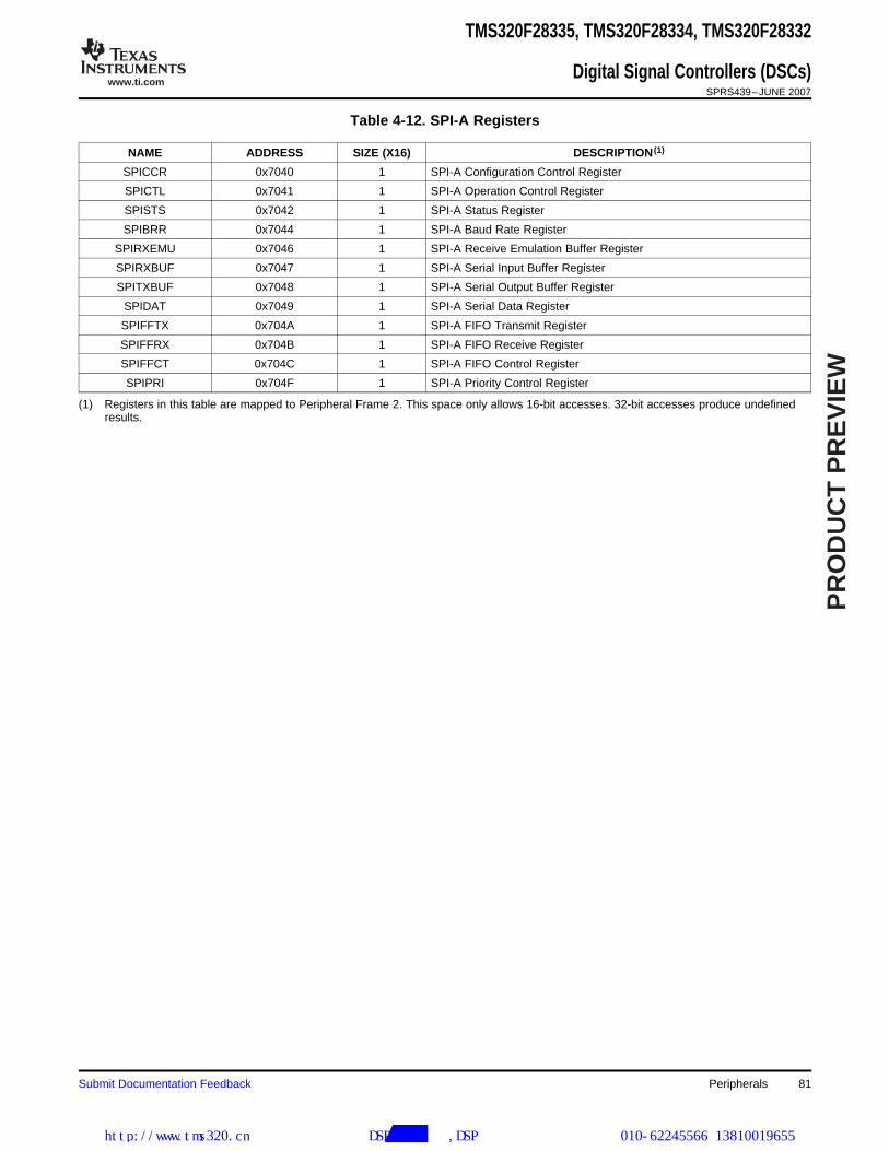
www.ti.com
PR
OD
UC
T P
RE
VIE
W
TMS320F28335, TMS320F28334, TMS320F28332
Digital Signal Controllers (DSCs)SPRS439–JUNE 2007
Table 4-12. SPI-A Registers
NAME ADDRESS SIZE (X16) DESCRIPTION (1)
SPICCR 0x7040 1 SPI-A Configuration Control Register
SPICTL 0x7041 1 SPI-A Operation Control Register
SPISTS 0x7042 1 SPI-A Status Register
SPIBRR 0x7044 1 SPI-A Baud Rate Register
SPIRXEMU 0x7046 1 SPI-A Receive Emulation Buffer Register
SPIRXBUF 0x7047 1 SPI-A Serial Input Buffer Register
SPITXBUF 0x7048 1 SPI-A Serial Output Buffer Register
SPIDAT 0x7049 1 SPI-A Serial Data Register
SPIFFTX 0x704A 1 SPI-A FIFO Transmit Register
SPIFFRX 0x704B 1 SPI-A FIFO Receive Register
SPIFFCT 0x704C 1 SPI-A FIFO Control Register
SPIPRI 0x704F 1 SPI-A Priority Control Register
(1) Registers in this table are mapped to Peripheral Frame 2. This space only allows 16-bit accesses. 32-bit accesses produce undefinedresults.
Submit Documentation Feedback Peripherals 81
http://www.tms320.cn 提供DSP芯片解密,DSP破解等服务 010-62245566 13810019655
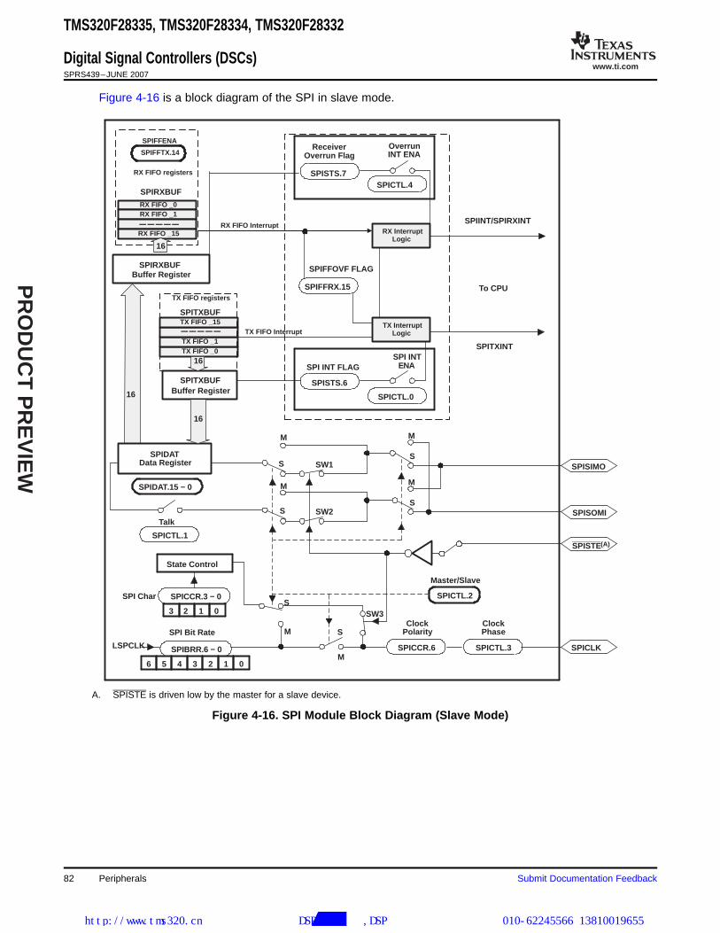
www.ti.com
PR
OD
UC
T P
RE
VIE
W S
SPICTL.0
SPI INT FLAGSPI INT
ENA
SPISTS.6
S
ClockPolarity
Talk
LSPCLK
456 123 0
0123
SPI Bit Rate
State Control
SPIRXBUFBuffer Register
ClockPhase
ReceiverOverrun Flag
SPICTL.4
OverrunINT ENA
SPICCR.3 − 0
SPIBRR.6 − 0 SPICCR.6 SPICTL.3
SPIDAT.15 − 0
SPICTL.1
M
S
M
Master/Slave
SPISTS.7
SPIDATData Register
M
S
SPICTL.2SPI Char
SPISIMO
SPISOMI
SPICLK
SW2
S
M
M
S
SW3
To CPU
M
SW1
SPITXBUFBuffer Register
RX FIFO _0RX FIFO _1
−−−−−RX FIFO _15
TX FIFO registers
TX FIFO _0TX FIFO _1−−−−−TX FIFO _15
RX FIFO registers
16
16
16
TX InterruptLogic
RX InterruptLogic
SPIINT/SPIRXINT
SPITXINT
SPIFFOVF FLAG
SPIFFRX.15
16
TX FIFO Interrupt
RX FIFO Interrupt
SPIRXBUF
SPITXBUF
SPIFFTX.14
SPIFFENA
SPISTE(A)
TMS320F28335, TMS320F28334, TMS320F28332
Digital Signal Controllers (DSCs)SPRS439–JUNE 2007
Figure 4-16 is a block diagram of the SPI in slave mode.
A. SPISTE is driven low by the master for a slave device.
Figure 4-16. SPI Module Block Diagram (Slave Mode)
82 Peripherals Submit Documentation Feedback
http://www.tms320.cn 提供DSP芯片解密,DSP破解等服务 010-62245566 13810019655

www.ti.com
PR
OD
UC
T P
RE
VIE
W
4.12 Inter-Integrated Circuit (I2C)
TMS320F28335, TMS320F28334, TMS320F28332
Digital Signal Controllers (DSCs)SPRS439–JUNE 2007
The 2833x device contains one I2C Serial Port. Figure 4-15 shows how the I2C peripheral moduleinterfaces within the 2833x device.
The I2C module has the following features:• Compliance with the Philips Semiconductors I2C-bus specification (version 2.1):
– Support for 1-bit to 8-bit format transfers– 7-bit and 10-bit addressing modes– General call– START byte mode– Support for multiple master-transmitters and slave-receivers– Support for multiple slave-transmitters and master-receivers– Combined master transmit/receive and receive/transmit mode– Data transfer rate of from 10 kbps up to 400 kbps (Philips Fast-mode rate)
• One 16-bit receive FIFO and one 16-bit transmit FIFO• One interrupt that can be used by the CPU. This interrupt can be generated as a result of one of the
following conditions:– Transmit-data ready– Receive-data ready– Register-access ready– No-acknowledgment received– Arbitration lost– Stop condition detected– Addressed as slave
• An additional interrupt that can be used by the CPU when in FIFO mode• Module enable/disable capability• Free data format mode
Submit Documentation Feedback Peripherals 83
http://www.tms320.cn 提供DSP芯片解密,DSP破解等服务 010-62245566 13810019655

www.ti.com
PR
OD
UC
T P
RE
VIE
W
SYSRS
Data[16]
SYSCLKOUT
Data[16]
Addr[16]
Control
I2CINT1A
I2CINT2A
C28X CPU
GPIOMUX
I2C−A
System ControlBlock
I2CAENCLK
PIEBlock
SDAA
SCLA
Per
iphe
ral B
us
TMS320F28335, TMS320F28334, TMS320F28332
Digital Signal Controllers (DSCs)SPRS439–JUNE 2007
A. The I2C registers are accessed at the SYSCLKOUT rate. The internal timing and signal waveforms of the I2C port arealso at the SYSCLKOUT rate.
B. The clock enable bit (I2CAENCLK) in the PCLKCRO register turns off the clock to the I2C port for low poweroperation. Upon reset, I2CAENCLK is clear, which indicates the peripheral internal clocks are off.
Figure 4-17. I2C Peripheral Module Interfaces
The registers in Table 4-13 configure and control the I2C port operation.
Table 4-13. I2C-A Registers
NAME ADDRESS DESCRIPTION
I2COAR 0x7900 I2C own address register
I2CIER 0x7901 I2C interrupt enable register
I2CSTR 0x7902 I2C status register
I2CCLKL 0x7903 I2C clock low-time divider register
I2CCLKH 0x7904 I2C clock high-time divider register
I2CCNT 0x7905 I2C data count register
I2CDRR 0x7906 I2C data receive register
I2CSAR 0x7907 I2C slave address register
I2CDXR 0x7908 I2C data transmit register
I2CMDR 0x7909 I2C mode register
I2CISRC 0x790A I2C interrupt source register
I2CPSC 0x790C I2C prescaler register
I2CFFTX 0x7920 I2C FIFO transmit register
I2CFFRX 0x7921 I2C FIFO receive register
I2CRSR - I2C receive shift register (not accessible to the CPU)
I2CXSR - I2C transmit shift register (not accessible to the CPU)
Peripherals84 Submit Documentation Feedback
http://www.tms320.cn 提供DSP芯片解密,DSP破解等服务 010-62245566 13810019655

www.ti.com
PR
OD
UC
T P
RE
VIE
W
4.13 GPIO MUX
GPxDAT (read)
InputQualification
GPxMUX1/2
High Impedance
Output Control
GPIOx pin
XRS
0 = Input, 1 = Output
Low PowerModes Block
GPxDIR (latch)
Peripheral 2 Input
Peripheral 3 Input
Peripheral 1 Output
Peripheral 2 Output
Peripheral 3 Output
Peripheral 1 Output Enable
Peripheral 2 Output Enable
Peripheral 3 Output Enable
00
01
10
11
00
01
10
11
00
01
10
11
GPxCTRL
Peripheral 1 Input
N/CGPxPUD
LPMCR0
InternalPullup
GPIOLMPSEL
GPxQSEL1/2
GPxSET
GPxDAT (latch)
GPxCLEAR
GPxTOGGLE
GPIOXINT1SEL
GPIOXINT2SEL
GPIOXNMISEL
= Default at Reset
PIEExternal InterruptMUX
Asynchronous path
Asynchronous path
TMS320F28335, TMS320F28334, TMS320F28332
Digital Signal Controllers (DSCs)SPRS439–JUNE 2007
On the 2833x devices, the GPIO MUX can multiplex up to three independent peripheral signals on asingle GPIO pin in addition to providing individual pin bit-banging IO capability. The GPIO MUX blockdiagram per pin is shown in Figure 4-18. Because of the open drain capabilities of the I2C pins, the GPIOMUX block diagram for these pins differ. See the TMS320x280x, 2801x, 2804x System Control andInterrupts Reference Guide (literature number SPRU712) for details.
A. x stands for the port, either A or B. For example, GPxDIR refers to either the GPADIR and GPBDIR registerdepending on the particular GPIO pin selected.
B. GPxDAT latch/read are accessed at the same memory location.
Figure 4-18. GPIO MUX Block Diagram
Submit Documentation Feedback Peripherals 85
http://www.tms320.cn 提供DSP芯片解密,DSP破解等服务 010-62245566 13810019655

www.ti.com
PR
OD
UC
T P
RE
VIE
W
TMS320F28335, TMS320F28334, TMS320F28332
Digital Signal Controllers (DSCs)SPRS439–JUNE 2007
The 2833x supports 88 GPIO pins. The GPIO control and data registers are mapped to Peripheral Frame1 to enable 32-bit operations on the registers (along with 16-bit operations). Table 4-14 shows the GPIOregister mapping.
Table 4-14. GPIO Registers
NAME ADDRESS SIZE (x16) DESCRIPTION
GPIO CONTROL REGISTERS (EALLOW PROTECTED)
GPACTRL 0x6F80 2 GPIO A Control Register (GPIO0 to 31)
GPAQSEL1 0x6F82 2 GPIO A Qualifier Select 1 Register (GPIO0 to 15)
GPAQSEL2 0x6F84 2 GPIO A Qualifier Select 2 Register (GPIO16 to 31)
GPAMUX1 0x6F86 2 GPIO A MUX 1 Register (GPIO0 to 15)
GPAMUX2 0x6F88 2 GPIO A MUX 2 Register (GPIO16 to 31)
GPADIR 0x6F8A 2 GPIO A Direction Register (GPIO0 to 31)
GPAPUD 0x6F8C 2 GPIO A Pull Up Disable Register (GPIO0 to 31)
0x6F8Ereserved 20x6F8F
GPBCTRL 0x6F90 2 GPIO B Control Register (GPIO32 to 35)
GPBQSEL1 0x6F92 2 GPIO B Qualifier Select 1 Register (GPIO32 to 35)
GPBQSEL2 0x6F94 2 reserved
GPBMUX1 0x6F96 2 GPIO B MUX 1 Register (GPIO32 to 35)
GPBMUX2 0x6F98 2 reserved
GPBDIR 0x6F9A 2 GPIO B Direction Register (GPIO32 to 35)
GPBPUD 0x6F9C 2 GPIO B Pull Up Disable Register (GPIO32 to 35)
0x6F9Ereserved 2 reserved0x6F9F
0x6FA0reserved 320x6FBF
GPIO DATA REGISTERS (NOT EALLOW PROTECTED)
GPADAT 0x6FC0 2 GPIO Data Register (GPIO0 to 31)
GPASET 0x6FC2 2 GPIO Data Set Register (GPIO0 to 31)
GPACLEAR 0x6FC4 2 GPIO Data Clear Register (GPIO0 to 31)
GPATOGGLE 0x6FC6 2 GPIO Data Toggle Register (GPIO0 to 31)
GPBDAT 0x6FC8 2 GPIO Data Register (GPIO32 to 35)
GPBSET 0x6FCA 2 GPIO Data Set Register (GPIO32 to 35)
GPBCLEAR 0x6FCC 2 GPIO Data Clear Register (GPIO32 to 35)
GPBTOGGLE 0x6FCE 2 GPIO Data Toggle Register (GPIO32 to 35)
0x6FD0reserved 160x6FDF
GPIO INTERRUPT AND LOW POWER MODES SELECT REGISTERS (EALLOW PROTECTED)
GPIOXINT1SEL 0x6FE0 1 XINT1 GPIO Input Select Register (GPIO0 to 31)
GPIOXINT2SEL 0x6FE1 1 XINT2 GPIO Input Select Register (GPIO0 to 31)
GPIOXNMISEL 0x6FE2 1 XNMI GPIO Input Select Register (GPIO0 to 31)
0x6FE3reserved 50x6FE7
GPIOLPMSEL 0x6FE8 2 LPM GPIO Select Register (GPIO0 to 31)
0x6FEAreserved 220x6FFF
Peripherals86 Submit Documentation Feedback
http://www.tms320.cn 提供DSP芯片解密,DSP破解等服务 010-62245566 13810019655
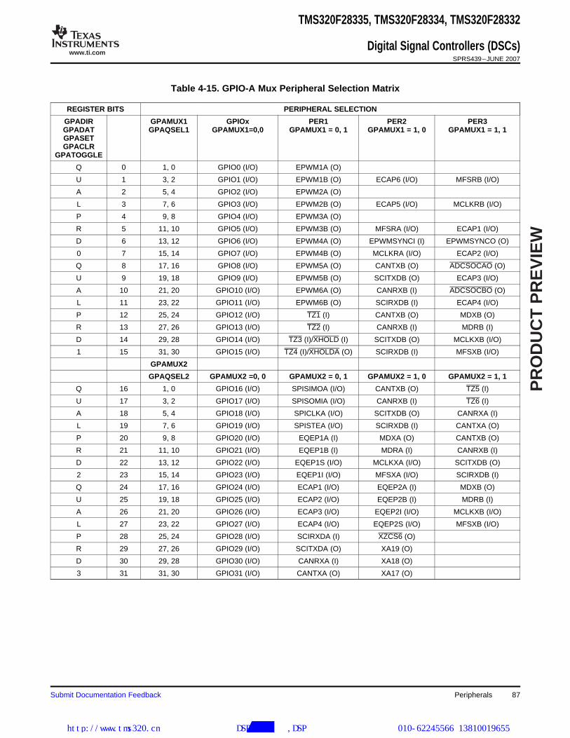
www.ti.com
PR
OD
UC
T P
RE
VIE
W
TMS320F28335, TMS320F28334, TMS320F28332
Digital Signal Controllers (DSCs)SPRS439–JUNE 2007
Table 4-15. GPIO-A Mux Peripheral Selection Matrix
REGISTER BITS PERIPHERAL SELECTION
GPADIR GPAMUX1 GPIOx PER1 PER2 PER3GPADAT GPAQSEL1 GPAMUX1=0,0 GPAMUX1 = 0, 1 GPAMUX1 = 1, 0 GPAMUX1 = 1, 1GPASETGPACLR
GPATOGGLE
Q 0 1, 0 GPIO0 (I/O) EPWM1A (O)
U 1 3, 2 GPIO1 (I/O) EPWM1B (O) ECAP6 (I/O) MFSRB (I/O)
A 2 5, 4 GPIO2 (I/O) EPWM2A (O)
L 3 7, 6 GPIO3 (I/O) EPWM2B (O) ECAP5 (I/O) MCLKRB (I/O)
P 4 9, 8 GPIO4 (I/O) EPWM3A (O)
R 5 11, 10 GPIO5 (I/O) EPWM3B (O) MFSRA (I/O) ECAP1 (I/O)
D 6 13, 12 GPIO6 (I/O) EPWM4A (O) EPWMSYNCI (I) EPWMSYNCO (O)
0 7 15, 14 GPIO7 (I/O) EPWM4B (O) MCLKRA (I/O) ECAP2 (I/O)
Q 8 17, 16 GPIO8 (I/O) EPWM5A (O) CANTXB (O) ADCSOCAO (O)
U 9 19, 18 GPIO9 (I/O) EPWM5B (O) SCITXDB (O) ECAP3 (I/O)
A 10 21, 20 GPIO10 (I/O) EPWM6A (O) CANRXB (I) ADCSOCBO (O)
L 11 23, 22 GPIO11 (I/O) EPWM6B (O) SCIRXDB (I) ECAP4 (I/O)
P 12 25, 24 GPIO12 (I/O) TZ1 (I) CANTXB (O) MDXB (O)
R 13 27, 26 GPIO13 (I/O) TZ2 (I) CANRXB (I) MDRB (I)
D 14 29, 28 GPIO14 (I/O) TZ3 (I)/XHOLD (I) SCITXDB (O) MCLKXB (I/O)
1 15 31, 30 GPIO15 (I/O) TZ4 (I)/XHOLDA (O) SCIRXDB (I) MFSXB (I/O)
GPAMUX2
GPAQSEL2 GPAMUX2 =0, 0 GPAMUX2 = 0, 1 GPAMUX2 = 1, 0 GPAMUX2 = 1, 1
Q 16 1, 0 GPIO16 (I/O) SPISIMOA (I/O) CANTXB (O) TZ5 (I)
U 17 3, 2 GPIO17 (I/O) SPISOMIA (I/O) CANRXB (I) TZ6 (I)
A 18 5, 4 GPIO18 (I/O) SPICLKA (I/O) SCITXDB (O) CANRXA (I)
L 19 7, 6 GPIO19 (I/O) SPISTEA (I/O) SCIRXDB (I) CANTXA (O)
P 20 9, 8 GPIO20 (I/O) EQEP1A (I) MDXA (O) CANTXB (O)
R 21 11, 10 GPIO21 (I/O) EQEP1B (I) MDRA (I) CANRXB (I)
D 22 13, 12 GPIO22 (I/O) EQEP1S (I/O) MCLKXA (I/O) SCITXDB (O)
2 23 15, 14 GPIO23 (I/O) EQEP1I (I/O) MFSXA (I/O) SCIRXDB (I)
Q 24 17, 16 GPIO24 (I/O) ECAP1 (I/O) EQEP2A (I) MDXB (O)
U 25 19, 18 GPIO25 (I/O) ECAP2 (I/O) EQEP2B (I) MDRB (I)
A 26 21, 20 GPIO26 (I/O) ECAP3 (I/O) EQEP2I (I/O) MCLKXB (I/O)
L 27 23, 22 GPIO27 (I/O) ECAP4 (I/O) EQEP2S (I/O) MFSXB (I/O)
P 28 25, 24 GPIO28 (I/O) SCIRXDA (I) XZCS6 (O)
R 29 27, 26 GPIO29 (I/O) SCITXDA (O) XA19 (O)
D 30 29, 28 GPIO30 (I/O) CANRXA (I) XA18 (O)
3 31 31, 30 GPIO31 (I/O) CANTXA (O) XA17 (O)
Submit Documentation Feedback Peripherals 87
http://www.tms320.cn 提供DSP芯片解密,DSP破解等服务 010-62245566 13810019655

www.ti.com
PR
OD
UC
T P
RE
VIE
W
TMS320F28335, TMS320F28334, TMS320F28332
Digital Signal Controllers (DSCs)SPRS439–JUNE 2007
Table 4-16. GPIO-B Mux Peripheral Selection Matrix
REGISTER BITS PERIPHERAL SELECTION
GPBDIR GPBMUX1 GPIOx PER1 PER2 PER3GPBDAT GPBQSEL1 GPBMUX1=0, 0 GPBMUX1 = 0, 1 GPBMUX1 = 1, 0 GPBMUX1 = 1, 1GPBSETGPBCLR
GPBTOGGLE
Q 0 1, 0 GPIO32 (I/O) SDAA (I/OC) (1) EPWMSYNCI (I) ADCSOCAO (O)
U 1 3, 2 GPIO33 (I/O) SCLA (I/OC) (1) EPWMSYNCO (O) ADCSOCBO (O)
A 2 5, 4 GPIO34 (I/O) ECAP1 (I/O) XREADY (I)
L 3 7, 6 GPIO35 (I/O) SCITXDA (O) XR/W (O)
P 4 9, 8 GPIO36 (I/O) SCIRXDA (I) XZCS0 (O)
R 5 11, 10 GPIO37 (I/O) ECAP2 (I/O) XZCS7 (O)
D 6 13, 12 GPIO38 (I/O) XWE0 (O)
0 7 15, 14 GPIO39 (I/O) XA16 (O)
Q 8 17, 16 GPIO40 (I/O) XA0/XWE1 (O)
U 9 19, 18 GPIO41 (I/O) XA1 (O)
A 10 21, 20 GPIO42 (I/O) XA2 (O)
L 11 23, 22 GPIO43 (I/O) XA3 (O)
P 12 25, 24 GPIO44 (I/O) XA4 (O)
R 13 27, 26 GPIO45 (I/O) XA5 (O)
D 14 29, 28 GPIO46 (I/O) XA6 (O)
1 15 31, 30 GPIO47 (I/O) XA7 (O)
GPBMUX2 GPBMUX2 =0, 0 GPBMUX2 = 0, 1 GPBMUX2 = 1, 0 GPBMUX2 = 1, 1GPBQSEL2
Q 16 1, 0 GPIO48 (I/O) ECAP5 (I/O) XD31 (I/O)
U 17 3, 2 GPIO49 (I/O) ECAP6 (I/O) XD30 (I/O)
A 18 5, 4 GPIO50 (I/O) EQEP1A (I) XD29 (I/O)
L 19 7, 6 GPIO51 (I/O) EQEP1B (I) XD28 (I/O)
P 20 9, 8 GPIO52 (I/O) EQEP1S (I/O) XD27 (I/O)
R 21 11, 10 GPIO53 (I/O) EQEP1I (I/O) XD26 (I/O)
D 22 13, 12 GPIO54 (I/O) SPISIMOA (I/O) XD25 (I/O)
2 23 15, 14 GPIO55 (I/O) SPISOMIA (I/O) XD24 (I/O)
Q 24 17, 16 GPIO56 (I/O) SPICLKA (I/O) XD23 (I/O)
U 25 19, 18 GPIO57 (I/O) SPISTEA (I/O) XD22 (I/O)
A 26 21, 20 GPIO58 (I/O) MCLKRA (I/O) XD21 (I/O)
L 27 23, 22 GPIO59 (I/O) MFSRA (I/O) XD20 (I/O)
P 28 25, 24 GPIO60 (I/O) MCLKRB (I/O) XD19 (I/O)
R 29 27, 26 GPIO61 (I/O) MFSRB (I/O) XD18 (I/O)
D 30 29, 28 GPIO62 (I/O) SCIRXDC (I) XD17 (I/O)
3 31 31, 30 GPIO63 (I/O) SCITXDC (O) XD16 (I/O)
(1) Open drain
88 Peripherals Submit Documentation Feedback
http://www.tms320.cn 提供DSP芯片解密,DSP破解等服务 010-62245566 13810019655

www.ti.com
PR
OD
UC
T P
RE
VIE
W
TMS320F28335, TMS320F28334, TMS320F28332
Digital Signal Controllers (DSCs)SPRS439–JUNE 2007
Table 4-17. GPIO-C Mux Peripheral Selection Matrix
REGISTER BITS PERIPHERAL SELECTION
GPCDIR GPCMUX1 GPIOx or PER1 PER2 or PER3GPCDAT GPCMUX1 = 0, 0 or 0, 1 GPCMUX1 = 1, 0 or 1, 1GPCSETGPCCLR
GPCTOGGLE
no 0 1, 0 GPIO64 (I/O) XD15 (I/O)
1 3, 2 GPIO65 (I/O) XD14 (I/O)
qu 2 5, 4 GPIO66 (I/O) XD13 (I/O)
a 3 7, 6 GPIO67 (I/O) XD12 (I/O)
l 4 9, 8 GPIO68 (I/O) XD11 (I/O)
5 11, 10 GPIO69 (I/O) XD10 (I/O)
6 13, 12 GPIO70 (I/O) XD9 (I/O)
7 15, 14 GPIO71 (I/O) XD8 (I/O)
no 8 17, 16 GPIO72 (I/O) XD7 (I/O)
9 19, 18 GPIO73 (I/O) XD6 (I/O)
qu 10 21, 20 GPIO74 (I/O) XD5 (I/O)
a 11 23, 22 GPIO75 (I/O) XD4 (I/O)
l 12 25, 24 GPIO76 (I/O) XD3 (I/O)
13 27, 26 GPIO77 (I/O) XD2 (I/O)
14 29, 28 GPIO78 (I/O) XD1 (I/O)
15 31, 30 GPIO79 (I/O) XD0 (I/O)
GPCMUX2 GPCMUX2 = 0, 0 or 0, 1 GPCMUX2 = 1, 0 or 1, 1
no 16 1, 0 GPIO80 (I/O) XA8 (O)
17 3, 2 GPIO81 (I/O) XA9 (O)
qu 18 5, 4 GPIO82 (I/O) XA10 (O)
a 19 7, 6 GPIO83 (I/O) XA11 (O)
l 20 9, 8 GPIO84 (I/O) XA12 (O)
21 11, 10 GPIO85 (I/O) XA13 (O)
22 13, 12 GPIO86 (I/O) XA14 (O)
23 15, 14 GPIO87 (I/O) XA15 (O)
The user can select the type of input qualification for each GPIO pin via the GPxQSEL1/2 registers fromfour choices:• Synchronization To SYSCLKOUT Only (GPxQSEL1/2=0, 0): This is the default mode of all GPIO pins
at reset and it simply synchronizes the input signal to the system clock (SYSCLKOUT).• Qualification Using Sampling Window (GPxQSEL1/2=0, 1 and 1, 0): In this mode the input signal, after
synchronization to the system clock (SYSCLKOUT), is qualified by a specified number of cycles beforethe input is allowed to change.
Submit Documentation Feedback Peripherals 89
http://www.tms320.cn 提供DSP芯片解密,DSP破解等服务 010-62245566 13810019655

www.ti.com
PR
OD
UC
T P
RE
VIE
W
GPyCTRL Reg
SYNC
SYSCLKOUT
Qualification Input Signal Qualified By 3 or 6 Samples
GPIOx
Time between samples
GPxQSEL
Number of Samples
TMS320F28335, TMS320F28334, TMS320F28332
Digital Signal Controllers (DSCs)SPRS439–JUNE 2007
Figure 4-19. Qualification Using Sampling Window
• The sampling period is specified by the QUALPRD bits in the GPxCTRL register and is configurable ingroups of 8 signals. It specifies a multiple of SYSCLKOUT cycles for sampling the input signal. Thesampling window is either 3-samples or 6-samples wide and the output is only changed when ALLsamples are the same (all 0s or all 1s) as shown in Figure 4-18 (for 6 sample mode).
• No Synchronization (GPxQSEL1/2=1,1): This mode is used for peripherals where synchronization isnot required (synchronization is performed within the peripheral).
Due to the multi-level multiplexing that is required on the 2833x device, there may be cases where aperipheral input signal can be mapped to more then one GPIO pin. Also, when an input signal is notselected, the input signal will default to either a 0 or 1 state, depending on the peripheral.
90 Peripherals Submit Documentation Feedback
http://www.tms320.cn 提供DSP芯片解密,DSP破解等服务 010-62245566 13810019655

www.ti.com
PR
OD
UC
T P
RE
VIE
W
5 Device Support
5.1 Device and Development Support Tool Nomenclature
TMS320F28335, TMS320F28334, TMS320F28332
Digital Signal Controllers (DSCs)SPRS439–JUNE 2007
Texas Instruments (TI) offers an extensive line of development tools for the C28x™ generation of DSCs,including tools to evaluate the performance of the processors, generate code, develop algorithmimplementations, and fully integrate and debug software and hardware modules.
The following products support development of 2833x-based applications:
Software Development Tools• Code Composer Studio™ Integrated Development Environment (IDE)
– C/C++ Compiler– Code generation tools– Assembler/Linker– Cycle Accurate Simulator
• Application algorithms• Sample applications code
Hardware Development Tools• 2833x development board• Evaluation modules• JTAG-based emulators - SPI515, XDS510PP, XDS510PP Plus, XDS510USB• Universal 5-V dc power supply• Documentation and cables
To designate the stages in the product development cycle, TI assigns prefixes to the part numbers of allTMS320™ DSC devices and support tools. Each TMS320™ DSP commercial family member has one ofthree prefixes: TMX, TMP, or TMS (e.g., TMS320F28335). Texas Instruments recommends two of threepossible prefix designators for its support tools: TMDX and TMDS. These prefixes represent evolutionarystages of product development from engineering prototypes (TMX/TMDX) through fully qualifiedproduction devices/tools (TMS/TMDS).
Device development evolutionary flow:
TMX Experimental device that is not necessarily representative of the final device's electricalspecifications
TMP Final silicon die that conforms to the device's electrical specifications but has not completedquality and reliability verification
TMS Fully qualified production device
Support tool development evolutionary flow:
TMDX Development-support product that has not yet completed Texas Instruments internal qualificationtesting
TMDS Fully qualified development-support product
TMX and TMP devices and TMDX development-support tools are shipped against the followingdisclaimer:"Developmental product is intended for internal evaluation purposes."
TMS devices and TMDS development-support tools have been characterized fully, and the quality andreliability of the device have been demonstrated fully. TI's standard warranty applies.
Submit Documentation Feedback Device Support 91
http://www.tms320.cn 提供DSP芯片解密,DSP破解等服务 010-62245566 13810019655

www.ti.com
PR
OD
UC
T P
RE
VIE
W
PREFIX
TMS 320 F 28335 PGF
TMX = experimental deviceTMP = prototype deviceTMS = qualified device
DEVICE FAMILY
320 = TMS320 DSP Family
TECHNOLOGY
PACKAGE TYPE
ZHH = 179-ball MicroStar BGA (lead-free)PGF = 176-pin LQFP
F = Flash EEPROM (1.8-V/1.9-V Core/3.3-V I/O)
DEVICE
283352833428332
BGA = Ball Grid Array
LQFP = Low-Profile Quad Flatpack
.ti.com/leadfree
TEMPERATURERANGE
A = −40°C to 85°C
A
TMS320F28335, TMS320F28334, TMS320F28332
Digital Signal Controllers (DSCs)SPRS439–JUNE 2007
Predictions show that prototype devices (TMX or TMP) have a greater failure rate than the standardproduction devices. Texas Instruments recommends that these devices not be used in any productionsystem because their expected end-use failure rate still is undefined. Only qualified production devices areto be used.
TI device nomenclature also includes a suffix with the device family name. This suffix indicates thepackage type (for example, PBK) and temperature range (for example, A). Figure 5-1 provides a legendfor reading the complete device name for any family member.
Figure 5-1. Example of 2833x Device Nomenclature
92 Device Support Submit Documentation Feedback
http://www.tms320.cn 提供DSP芯片解密,DSP破解等服务 010-62245566 13810019655

www.ti.com
PR
OD
UC
T P
RE
VIE
W
5.2 Documentation Support
TMS320F28335, TMS320F28334, TMS320F28332
Digital Signal Controllers (DSCs)SPRS439–JUNE 2007
Extensive documentation supports all of the TMS320™ DSP family generations of devices from productannouncement through applications development. The types of documentation available include: datasheets and data manuals, with design specifications; and hardware and software applications. Usefulreference documentation includes:
CPU User's GuidesSPRU430 TMS320C28x DSP CPU and Instruction Set Reference Guide describes the central
processing unit (CPU) and the assembly language instructions of the TMS320C28xfixed-point digital signal processors (DSPs). It also describes emulation features available onthese DSPs.
SPRUEO2 TMS320C28x Floating Point Unit and Instruction Set Reference Guide describes thefloating-point unit and includes the instructions for the FPU.
Peripheral GuidesSPRU566 TMS320x28xx, 28xxx Peripheral Reference Guide describes the peripheral reference guides
of the 28x digital signal processors (DSPs).
SPRU716 TMS320x280x, 2801x, 2804x Analog-to-Digital Converter (ADC) Reference Guide describeshow to configure and use the on-chip ADC module, which is a 12-bit pipelined ADC.
SPRU791 TMS320x28xx, 28xxx Enhanced Pulse Width Modulator (ePWM) Module Reference Guidedescribes the main areas of the enhanced pulse width modulator that include digital motorcontrol, switch mode power supply control, UPS (uninterruptible power supplies), and otherforms of power conversion
SPRU924 TMS320x28xx, 28xxx High-Resolution Pulse Width Modulator (HRPWM) describes theoperation of the high-resolution extension to the pulse width modulator (HRPWM)
SPRU807 TMS320x28xx, 28xxx Enhanced Capture (eCAP) Module Reference Guide describes theenhanced capture module. It includes the module description and registers.
SPRU790 TMS320x28xx, 28xxx Enhanced Quadrature Encoder Pulse (eQEP) Reference Guidedescribes the eQEP module, which is used for interfacing with a linear or rotary incrementalencoder to get position, direction, and speed information from a rotating machine in highperformance motion and position control systems. It includes the module description andregisters
SPRU074 TMS320x28xx, 28xxx Enhanced Controller Area Network (eCAN) Reference Guidedescribes the eCAN that uses established protocol to communicate serially with othercontrollers in electrically noisy environments.
SPRU051 TMS320x28xx, 28xxx Serial Communication Interface (SCI) Reference Guide describes theSCI, which is a two-wire asynchronous serial port, commonly known as a UART. The SCImodules support digital communications between the CPU and other asynchronousperipherals that use the standard non-return-to-zero (NRZ) format.
SPRU059 TMS320x28xx, 28xxx Serial Peripheral Interface (SPI) Reference Guide describes the SPI -a high-speed synchronous serial input/output (I/O) port - that allows a serial bit stream ofprogrammed length (one to sixteen bits) to be shifted into and out of the device at aprogrammed bit-transfer rate.
SPRU721 TMS320x28xx, 28xxx Inter-Integrated Circuit (I2C) Reference Guide describes the featuresand operation of the inter-integrated circuit (I2C) module that is available on theTMS320x280x digital signal processor (DSP).
Tools GuidesSPRU513 TMS320C28x Assembly Language Tools User's Guide describes the assembly language
tools (assembler and other tools used to develop assembly language code), assembler
Submit Documentation Feedback Device Support 93
http://www.tms320.cn 提供DSP芯片解密,DSP破解等服务 010-62245566 13810019655

www.ti.com
PR
OD
UC
T P
RE
VIE
W
TMS320F28335, TMS320F28334, TMS320F28332
Digital Signal Controllers (DSCs)SPRS439–JUNE 2007
directives, macros, common object file format, and symbolic debugging directives for theTMS320C28x device.
SPRU514 TMS320C28x Optimizing C Compiler User's Guide describes the TMS320C28x™ C/C++compiler. This compiler accepts ANSI standard C/C++ source code and produces TMS320DSP assembly language source code for the TMS320C28x device.
SPRU608 The TMS320C28x Instruction Set Simulator Technical Overview describes the simulator,available within the Code Composer Studio for TMS320C2000 IDE, that simulates theinstruction set of the C28x™ core.
SPRU625 TMS320C28x DSP/BIOS Application Programming Interface (API) Reference Guidedescribes development using DSP/BIOS.
Application Reports
SPRAAM0 Getting Started With TMS320C28x™ Digital Signal Controllers is organized by developmentflow and functional areas to make your design effort as seamless as possible. Tips ongetting started with C28x™ DSP software and hardware development are provided to aid inyour initial design and debug efforts. Each section includes pointers to valuable informationincluding technical documentation, software, and tools for use in each phase of design.
SPRAAD5 Power Line Communication for Lighting Apps using BPSK w/ a Single DSP Controllerpresents a complete implementation of a power line modem following CEA-709 protocolusing a single DSP.
SPRAA85 Programming TMS320x28xx and 28xxx Peripherals in C/C++ explores a hardwareabstraction layer implementation to make C/C++ coding easier on 28x DSPs. This method iscompared to traditional #define macros and topics of code efficiency and special caseregisters are also addressed.
SPRA958 Running an Application from Internal Flash Memory on the TMS320F28xx DSP covers therequirements needed to properly configure application software for execution from on-chipflash memory. Requirements for both DSP/BIOS™ and non-DSP/BIOS projects arepresented. Example code projects are included.
SPRAA91 TMS320F280x DSC USB Connectivity Using TUSB3410 USB-to-UART Bridge Chip presentshardware connections as well as software preparation and operation of the developmentsystem using a simple communication echo program.
SPRAA58 TMS320x281x to TMS320x280x Migration Overview describes differences between theTexas Instruments TMS320x281x and TMS320x280x DSPs to assist in application migrationfrom the 281x to the 280x. While the main focus of this document is migration from 281x to280x, users considering migrating in the reverse direction (280x to 281x) will also find thisdocument useful.
SPRAAD8 TMS320280x and TMS320F2801x ADC Calibration describes a method for improving theabsolute accuracy of the 12-bit ADC found on the TMS320280x and TMS3202801x devices.Inherent gain and offset errors affect the absolute accuracy of the ADC. The methodsdescribed in this report can improve the absolute accuracy of the ADC to levels better than0.5%. This application report has an option to download an example program that executesfrom RAM on the F2808 EzDSP.
SPRAAI1 Using Enhanced Pulse Width Modulator (ePWM) Module for 0-100% Duty Cycle Controlprovides a guide for the use of the ePWM module to provide 0% to 100% duty cycle controland is applicable to the TMS320x280x family of processors.
SPRAA88 Using PWM Output as a Digital-to-Analog Converter on a TMS320F280x presents a methodfor utilizing the on-chip pulse width modulated (PWM) signal generators on theTMS320F280x family of digital signal controllers as a digital-to-analog converter (DAC).
Device Support94 Submit Documentation Feedback
http://www.tms320.cn 提供DSP芯片解密,DSP破解等服务 010-62245566 13810019655

www.ti.com
PR
OD
UC
T P
RE
VIE
W
TMS320F28335, TMS320F28334, TMS320F28332
Digital Signal Controllers (DSCs)SPRS439–JUNE 2007
SPRAAH1 Using the Enhanced Quadrature Encoder Pulse (eQEP) Module provides a guide for the useof the eQEP module as a dedicated capture unit and is applicable to the TMS320x280x,28xxx family of processors.
SPRA820 Online Stack Overflow Detection on the TMS320C28x DSP presents the methodology foronline stack overflow detection on the TMS320C28x™ DSP. C-source code is provided thatcontains functions for implementing the overflow detection on both DSP/BIOS™ andnon-DSP/BIOS applications.
SPRA806 An Easy Way of Creating a C-callable Assembly Function for the TMS320C28x DSPprovides instructions and suggestions to configure the C compiler to assist withunderstanding of parameter-passing conventions and environments expected by the Ccompiler.
A series of DSP textbooks is published by Prentice-Hall and John Wiley & Sons to support digital signalprocessing research and education. The TMS320 DSP newsletter, Details on Signal Processing, ispublished quarterly and distributed to update TMS320 DSP customers on product information.
Updated information on the TMS320 DSP controllers can be found on the worldwide web at:http://www.ti.com.
To send comments regarding this data manual (literature number SPRS230), use [email protected] email address, which is a repository for feedback. For questions and support,contact the Product Information Center listed at the http://www.ti.com/sc/docs/pic/home.htm site.
Submit Documentation Feedback Device Support 95
http://www.tms320.cn 提供DSP芯片解密,DSP破解等服务 010-62245566 13810019655

www.ti.com
PR
OD
UC
T P
RE
VIE
W
6 Electrical Specifications
6.1 Absolute Maximum Ratings (1) (2)
TMS320F28335, TMS320F28334, TMS320F28332
Digital Signal Controllers (DSCs)SPRS439–JUNE 2007
This section provides the absolute maximum ratings and the recommended operating conditions.
Unless otherwise noted, the list of absolute maximum ratings are specified over operating temperature ranges.Supply voltage range, VDDIO, VDD3VFL with respect to VSS - 0.3 V to 4.6 V
Supply voltage range, VDDA2, VDDAIO with respect to VSSA - 0.3 V to 4.6 V
Supply voltage range, VDD with respect to VSS - 0.3 V to 2.5 V
Supply voltage range, VDD1A18, VDD2A18 with respect to VSSA - 0.3 V to 2.5 V
Supply voltage range, VSSA2, VSSAIO, VSS1AGND, VSS2AGND with respect to VSS - 0.3 V to 0.3 V
Input voltage range, VIN - 0.3 V to 4.6 V
Output voltage range, VO - 0.3 V to 4.6 V
Input clamp current, IIK (VIN < 0 or VIN > VDDIO) (3) ± 20 mA
Output clamp current, IOK (VO < 0 or VO > VDDIO) ± 20 mA
Operating ambient temperature ranges, TA: A version (4) - 40°C to 85°C
Junction temperature range, Tj(4) - 40°C to 150°C
Storage temperature range, Tstg(4) - 65°C to 150°C
(1) Stresses beyond those listed under Absolute Maximum Ratings may cause permanent damage to the device. These are stress ratingsonly, and functional operation of the device at these or any other conditions beyond those indicated under Section 6.2 is not implied.Exposure to absolute-maximum-rated conditions for extended periods may affect device reliability.
(2) All voltage values are with respect to VSS, unless otherwise noted.(3) Continuous clamp current per pin is ± 2 mA. This includes the analog inputs which have an internal clamping circuit that clamps the
voltage to a diode drop above VDDA2 or below VSSA2.(4) Long-term high-temperature storage and/or extended use at maximum temperature conditions may result in a reduction of overall device
life. For additional information, see IC Package Thermal Metrics Application Report (literature number SPRA953) and Reliability Data forTMS320LF24x and TMS320F281x Devices Application Report (literature number SPRA963)
Electrical Specifications96 Submit Documentation Feedback
http://www.tms320.cn 提供DSP芯片解密,DSP破解等服务 010-62245566 13810019655

www.ti.com
PR
OD
UC
T P
RE
VIE
W
6.2 Recommended Operating Conditions
6.3 Electrical Characteristics
TMS320F28335, TMS320F28334, TMS320F28332
Digital Signal Controllers (DSCs)SPRS439–JUNE 2007
over operating free-air temperature range (unless otherwise noted)MIN NOM MAX UNIT
Device supply voltage, I/O, VDDIO 3.2 3.3 3.4 V
Device supply voltage CPU, VDD 1.84 1.9 1.96 V
Supply ground, VSS, VSSIO 0 V
ADC supply voltage (3.3 V), VDDA2, VDDAIO 3.2 3.3 3.4 V
ADC supply voltage (1.8 V), VDD1A18, VDD2A18 1.84 1.9 1.96 V
Flash supply voltage, VDD3VFL 3.2 3.3 3.4 V
Device clock frequency (system clock), fSYSCLKOUT 150-MHz devices 2 150 MHz
100-MHz devices 2 100 MHz
High-level input voltage, VIH 2 VDDIO V
Low-level input voltage, VIL 0.8
All I/Os except Group 2 -4 mAHigh-level output source current, VOH = 2.4 V, IOH
Group 2 (1) -8
All I/Os except Group 2 4 mALow-level output sink current, VOL = VOL MAX, IOL
Group 2 (1) 8
Ambient temperature, TA A version -40 85
(1) Group 2 pins are as follows: GPIO28, GPIO29, GPIO30, GPIO31, TDO, XCLKOUT, EMU0, EMU1, XINTF pins, GPIO35-87, XRD.
over recommended operating conditions (unless otherwise noted)PARAMETER TEST CONDITIONS MIN TYP MAX UNIT
IOH = IOHMAX 2.4VOH High-level output voltage V
IOH = 50 µA VDDIO - 0.2
VOL Low-level output voltage IOL = IOLMAX 0.4 V
Pin with pullup VDDIO = 3.3 V, VIN = 0 V All I/Os (including XRS) -80 -140 -190enabledInput currentIIL µA(low level) Pin with pulldown VDDIO = 3.3 V, VIN = 0 V ±2enabled
Pin with pullup VDDIO = 3.3 V, VIN = VDDIO ±2enabled
Input current Pin with pulldownIIH VDDIO = 3.3 V, VIN = VDDIO 28 50 80 µA(high level) enabled
Pin with pulldown VDDIO = 3.3 V, VIN = VDDIO 80 140 190enabled
Output current, pullup orIOZ VO = VDDIO or 0 V ±2 µApulldown disabled
CI Input capacitance 2 pF
Submit Documentation Feedback Electrical Specifications 97
http://www.tms320.cn 提供DSP芯片解密,DSP破解等服务 010-62245566 13810019655
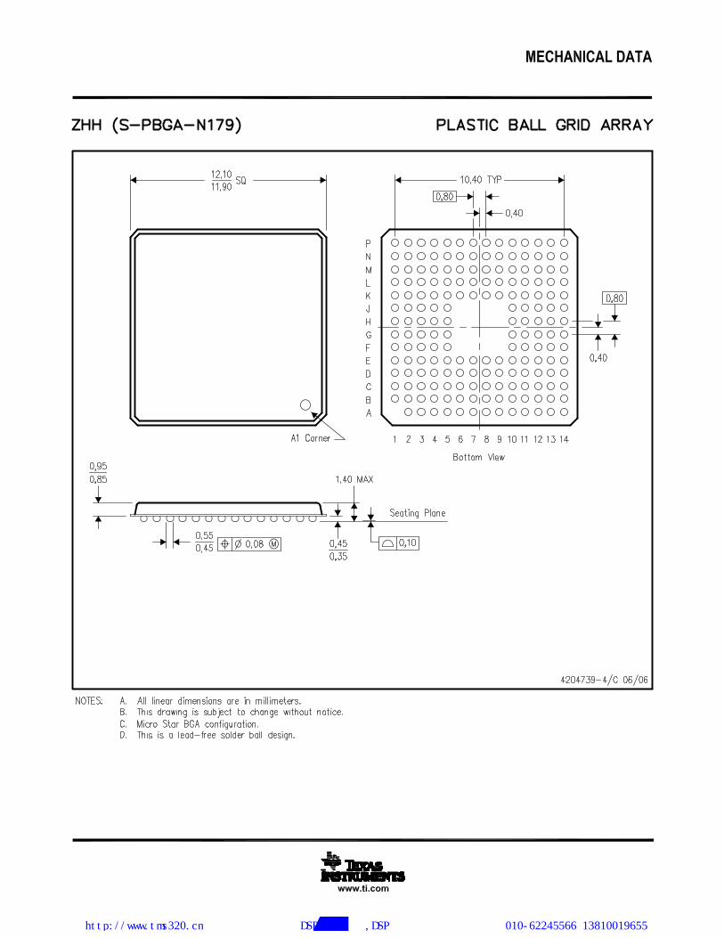
http://www.tms320.cn 提供DSP芯片解密,DSP破解等服务 010-62245566 13810019655

OCTOBER 1994
1POST OFFICE BOX 655303 • DALLAS, TEXAS 75265
PGF (S-PQFP-G176) PLASTIC QUAD FLATPACK
0,13 NOM
89
0,170,27
88
45
0,45
0,25
0,75
44
Seating Plane
0,05 MIN
4040134/B 03/95
Gage Plane
132
133
176
SQ24,20
SQ25,8026,20
23,80
21,50 SQ1
1,451,35
1,60 MAX
M0,08
0,50
0,08
0°−7°
NOTES: A. All linear dimensions are in millimeters.B. This drawing is subject to change without notice.C. Falls within JEDEC MO-136
http://www.tms320.cn 提供DSP芯片解密,DSP破解等服务 010-62245566 13810019655

IMPORTANT NOTICE
Texas Instruments Incorporated and its subsidiaries (TI) reserve the right to make corrections, modifications, enhancements,improvements, and other changes to its products and services at any time and to discontinue any product or service without notice.Customers should obtain the latest relevant information before placing orders and should verify that such information is current andcomplete. All products are sold subject to TI’s terms and conditions of sale supplied at the time of order acknowledgment.
TI warrants performance of its hardware products to the specifications applicable at the time of sale in accordance with TI’sstandard warranty. Testing and other quality control techniques are used to the extent TI deems necessary to support thiswarranty. Except where mandated by government requirements, testing of all parameters of each product is not necessarilyperformed.
TI assumes no liability for applications assistance or customer product design. Customers are responsible for their products andapplications using TI components. To minimize the risks associated with customer products and applications, customers shouldprovide adequate design and operating safeguards.
TI does not warrant or represent that any license, either express or implied, is granted under any TI patent right, copyright, maskwork right, or other TI intellectual property right relating to any combination, machine, or process in which TI products or servicesare used. Information published by TI regarding third-party products or services does not constitute a license from TI to use suchproducts or services or a warranty or endorsement thereof. Use of such information may require a license from a third party underthe patents or other intellectual property of the third party, or a license from TI under the patents or other intellectual property of TI.
Reproduction of TI information in TI data books or data sheets is permissible only if reproduction is without alteration and isaccompanied by all associated warranties, conditions, limitations, and notices. Reproduction of this information with alteration is anunfair and deceptive business practice. TI is not responsible or liable for such altered documentation. Information of third partiesmay be subject to additional restrictions.
Resale of TI products or services with statements different from or beyond the parameters stated by TI for that product or servicevoids all express and any implied warranties for the associated TI product or service and is an unfair and deceptive businesspractice. TI is not responsible or liable for any such statements.
TI products are not authorized for use in safety-critical applications (such as life support) where a failure of the TI product wouldreasonably be expected to cause severe personal injury or death, unless officers of the parties have executed an agreementspecifically governing such use. Buyers represent that they have all necessary expertise in the safety and regulatory ramificationsof their applications, and acknowledge and agree that they are solely responsible for all legal, regulatory and safety-relatedrequirements concerning their products and any use of TI products in such safety-critical applications, notwithstanding anyapplications-related information or support that may be provided by TI. Further, Buyers must fully indemnify TI and itsrepresentatives against any damages arising out of the use of TI products in such safety-critical applications.
TI products are neither designed nor intended for use in military/aerospace applications or environments unless the TI products arespecifically designated by TI as military-grade or "enhanced plastic." Only products designated by TI as military-grade meet militaryspecifications. Buyers acknowledge and agree that any such use of TI products which TI has not designated as military-grade issolely at the Buyer's risk, and that they are solely responsible for compliance with all legal and regulatory requirements inconnection with such use.
TI products are neither designed nor intended for use in automotive applications or environments unless the specific TI productsare designated by TI as compliant with ISO/TS 16949 requirements. Buyers acknowledge and agree that, if they use anynon-designated products in automotive applications, TI will not be responsible for any failure to meet such requirements.
Following are URLs where you can obtain information on other Texas Instruments products and application solutions:
Products Applications
Amplifiers amplifier.ti.com Audio www.ti.com/audio
Data Converters dataconverter.ti.com Automotive www.ti.com/automotive
DSP dsp.ti.com Broadband www.ti.com/broadband
Interface interface.ti.com Digital Control www.ti.com/digitalcontrol
Logic logic.ti.com Military www.ti.com/military
Power Mgmt power.ti.com Optical Networking www.ti.com/opticalnetwork
Microcontrollers microcontroller.ti.com Security www.ti.com/security
RFID www.ti-rfid.com Telephony www.ti.com/telephony
Low Power www.ti.com/lpw Video & Imaging www.ti.com/videoWireless
Wireless www.ti.com/wireless
Mailing Address: Texas Instruments, Post Office Box 655303, Dallas, Texas 75265Copyright © 2007, Texas Instruments Incorporated
http://www.tms320.cn 提供DSP芯片解密,DSP破解等服务 010-62245566 13810019655
Recommended


![cesamiæ ä½ ã ã ã ¥ã ¢ã «ï¼ å ©ç ¨è ï¼ .ppt [äº æ 㠢㠼ã ]](https://img.pdfslide.us/doc/110x75/61e096d23e6110489c3fa9c0/cesami-.jpg)