TLC2654, TLC2654AAdvanced LinCMOS LOW-NOISE CHOPPER-STABILIZED
OPERATIONAL AMPLIFIERS
SLOS020G – NOVEMBER 1988 – REVISED APRIL 2001
1POST OFFICE BOX 655303 • DALLAS, TEXAS 75265
Input Noise Voltage0.5 µV (Peak-to-Peak) Typ, f = 0 to 1 Hz1.5 µV (Peak-to-Peak) Typ, f = 0 to 10 Hz47 nV/√Hz Typ, f = 10 Hz13 nV/√Hz Typ, f = 1 kHz
High Chopping Frequency . . . 10 kHz Typ
No Clock Noise Below 10 kHz
No Intermodulation Error Below 5 kHz
Low Input Offset Voltage10 µV Max (TLC2654A)
Excellent Offset Voltage StabilityWith Temperature . . . 0.05 µV/°C Max
AVD . . . 135 dB Min (TLC2654A)
CMRR . . . 110 dB Min (TLC2654A)
kSVR . . . 110 dB Min
Single-Supply Operation
Common-Mode Input Voltage RangeIncludes the Negative Rail
No Noise Degradation With ExternalCapacitors Connected to VDD–
Available in Q-Temp Automotive HighRel Automotive ApplicationsConfiguration Control/Print SupportQualification to Automotive Standards
description
The TLC2654 and TLC2654A are low-noisechopper-stabilized operational amplifiers usingthe Advanced LinCMOS process. Combiningthis process with chopper-stabilization circuitrymakes excellent dc precision possible. In addition,circuit techniques are added that give theTLC2654 and TLC2654A superior noise perfor-mance.
Chopper-stabilization techniques provide for extremely high dc precision by continuously nulling input offsetvoltage even during variations in temperature, time, common-mode voltage, and power-supply voltage. Thehigh chopping frequency of the TLC2654 and TLC2654A (see Figure 1) provides excellent noise performancein a frequency spectrum from near dc to 10 kHz. In addition, intermodulation or aliasing error is eliminated fromfrequencies up to 5 kHz.
This high dc precision and low noise, coupled with the extremely high input impedance of the CMOS input stage,makes the TLC2654 and TLC2654A ideal choices for a broad range of applications such as low-level,low-frequency thermocouple amplifiers and strain gauges and wide-bandwidth and subsonic circuits. Forapplications requiring even greater dc precision, use the TLC2652 or TLC2652A devices, which have achopping frequency of 450 Hz.
Copyright 2001, Texas Instruments IncorporatedPRODUCTION DATA information is current as of publication date.Products conform to specifications per the terms of Texas Instrumentsstandard warranty. Production processing does not necessarily includetesting of all parameters.
Please be aware that an important notice concerning availability, standard warranty, and use in critical applications ofTexas Instruments semiconductor products and disclaimers thereto appears at the end of this data sheet.
On products compliant to MIL-PRF-38535, all parameters are testedunless otherwise noted. On all other products, productionprocessing does not necessarily include testing of all parameters.
Advanced LinCMOS is a trademark of Texas Instruments.
1
2
3
4
8
7
6
5
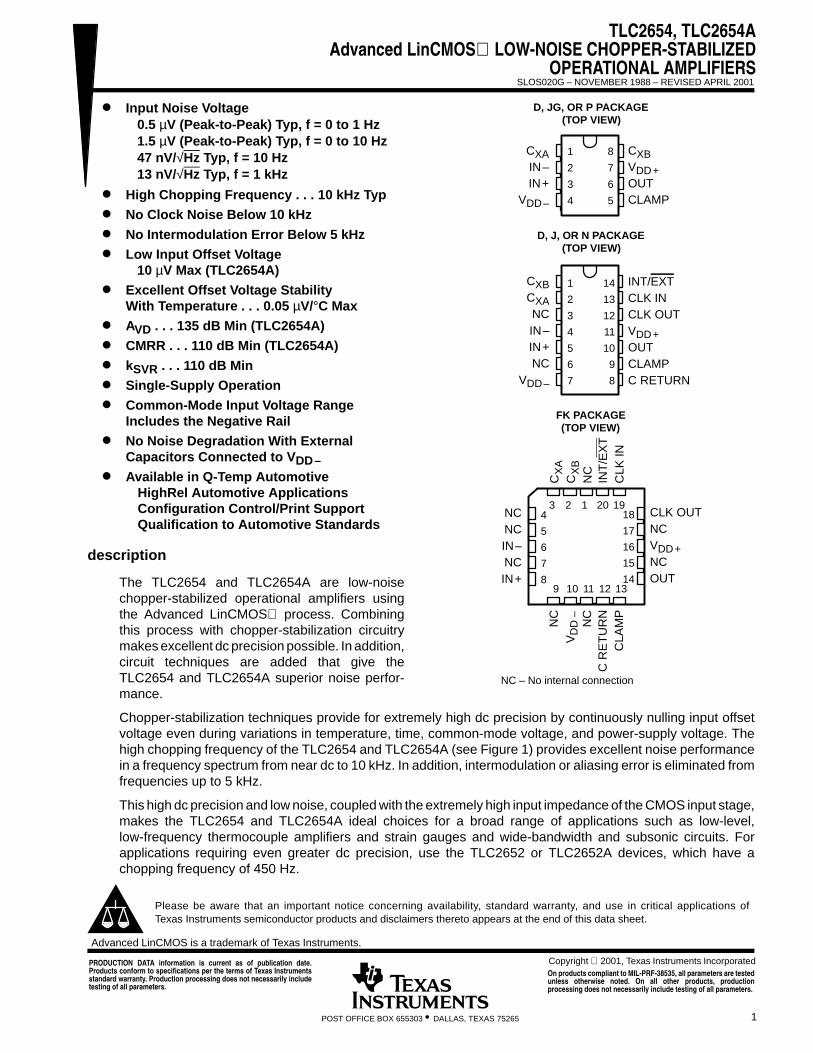
CXAIN–IN+
VDD–
CXBVDD+OUTCLAMP
D, JG, OR P PACKAGE
1
2
3
4
5
6
7
14
13
12
11
10
9
8
CXBCXANCIN–IN+NC
VDD–
INT/EXTCLK INCLK OUTVDD+OUTCLAMPC RETURN
D, J, OR N PACKAGE(TOP VIEW)
NC – No internal connection
3 2 1 20 19
9 10 11 12 13
4
5
6
7
8
18
17
16
15
14
CLK OUTNCVDD+NCOUT
NCNCIN–NCIN+
FK PACKAGE(TOP VIEW)
C C NC
C R
ET
UR
NC
LAM
PIN
T/E
XT
CLK
IN
NC
V
NC
XA
XB
DD
–
(TOP VIEW)

TLC2654, TLC2654AAdvanced LinCMOS LOW-NOISE CHOPPER-STABILIZEDOPERATIONAL AMPLIFIERS
SLOS020G – NOVEMBER 1988 – REVISED APRIL 2001
2 POST OFFICE BOX 655303 • DALLAS, TEXAS 75265
description (continued)
The TLC2654 and TLC2654A common-modeinput voltage range includes the negative rail,thereby providing superior performance in eithersingle-supply or split-supply applications, even atpower supply voltage levels as low as ±2.3 V.
Two external capacitors are required to operatethe device; however, the on-chip chopper-controlcircuitry is transparent to the user. On devices inthe 14-pin and 20-pin packages, the controlcircuitry is accessible, allowing the user the optionof controlling the clock frequency with an externalfrequency source. In addition, the clock thresholdof the TLC2554 and TLC2654A requires no levelshifting when used in the single-supply configura-tion with a normal CMOS or TTL clock input.
Innovative circuit techniques used on theTLC2654 and TLC2654A allow exceptionally fastoverload recovery time. An output clamp pin isavailable to reduce the recovery time even further.
The device inputs and outputs are designed towithstand –100-mA surge currents withoutsustaining latch-up. In addition, the TLC2654 and TLC2654A incorporate internal ESD-protection circuits thatprevent functional failures at voltages up to 2000 V as tested under MIL-STD-883C, Method 3015; however,exercise care in handling these devices, as exposure to ESD may result in degradation of the device parametricperformance.
The C-suffix devices are characterized for operation from 0°C to 70°C. The I-suffix devices are characterizedfor operation from –40°C to 85°C. The Q-suffix devices are characterized for operation from –40°C to 125°C.The M-suffix devices are characterized for operation over the full military temperature range of –55°C to125°C.
AVAILABLE OPTIONS
PACKAGED DEVICES
TVIOmax 8 PIN 14 PIN 20 PIN
TAVIOmaxAT 25°C SMALL
OUTLINE(D)
CERAMICDIP(JG)
PLASTICDIP(P)
SMALLOUTLINE
(D)
CERAMICDIP(J)
PLASTICDIP(N)
CERAMICDIP(FK)
10 µV TLC2654AC-8D — TLC2654ACP TLC2654AC-14D — TLC2654ACN —0°C to 70°C
10 µV20 mV
TLC2654AC-8DTLC2654C 8D
— TLC2654ACPTLC2654CP
TLC2654AC-14DTLC2654C 14D
— TLC2654ACNTLC2654CN
—20 mV TLC2654C-8D — TLC2654CP TLC2654C-14D — TLC2654CN —
10 µV TLC2654AI-8D — TLC2654AIP TLC2654AI-14D — TLC2654AIN —– 40°C to 85°C
10 µV20 µV
TLC2654AI-8DTLC2654I 8D
— TLC2654AIPTLC2654IP
TLC2654AI-14DTLC2654I 14D
— TLC2654AINTLC2654IN
—20 µV TLC2654I-8D — TLC2654IP TLC2654I-14D — TLC2654IN —
10 µV TLC2654AQ-8D — — — — — —– 40°C to 125°C
10 µV20 µV
TLC2654AQ-8DTLC2654Q 8D
— — — — — —20 µV TLC2654Q-8D — — — — — —
10 µV TLC2654AM-8D TLC2654AMJG TLC2654AMP TLC2654AM-14D TLC2654AMJ TLC2654AMN TLC2654AMFK– 55°C to 125°C
10 µV20 µV
TLC2654AM-8DTLC2654M 8D
TLC2654AMJGTLC2654MJG
TLC2654AMPTLC2654MP
TLC2654AM-14DTLC2654M 14D
TLC2654AMJTLC2654MJ
TLC2654AMNTLC2654MN
TLC2654AMFKTLC2654MFK20 µV TLC2654M-8D TLC2654MJG TLC2654MP TLC2654M-14D TLC2654MJ TLC2654MN TLC2654MFK
The 8-pin and 14-pin D packages are available taped and reeled. Add R suffix to device type (e.g., TLC2654AC-8DR).
Vn
– E
qu
ival
ent
Inp
ut
No
ise
Vo
ltag
e –
nV
/XX
VZ
EQUIVALENT INPUT NOISE VOLTAGEvs
FREQUENCY
1 k
100
101 10 100
f – Frequency – Hz
1 k
10 k
Vn
nV
/H
z
Typical 250-HzChopper-StabilizedOperational Amplifier
TLC2654
Figure 1

TLC2654, TLC2654AAdvanced LinCMOS LOW-NOISE CHOPPER-STABILIZED
OPERATIONAL AMPLIFIERS
SLOS020G – NOVEMBER 1988 – REVISED APRIL 2001
3POST OFFICE BOX 655303 • DALLAS, TEXAS 75265
functional block diagram
External Components
C RETURNVDD–
Null
IN+IN–
VDD+
MainCIC
CLAMP
OUT
CXB CXA
ClampCircuit
Compensation-BiasingCircuit
A
A
ABB
B
5
4
11
1 2
7 8
9
10+–
+–
Pin numbers shown are for the D (14 pin), J, and N packages.
TLC2654, TLC2654AAdvanced LinCMOS LOW-NOISE CHOPPER-STABILIZEDOPERATIONAL AMPLIFIERS
SLOS020G – NOVEMBER 1988 – REVISED APRIL 2001
4 POST OFFICE BOX 655303 • DALLAS, TEXAS 75265
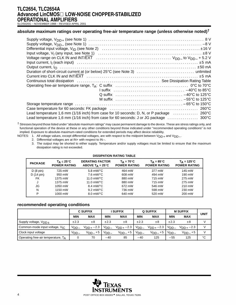
absolute maximum ratings over operating free-air temperature range (unless otherwise noted)†
Supply voltage, VDD+ (see Note 1) 8 V. . . . . . . . . . . . . . . . . . . . . . . . . . . . . . . . . . . . . . . . . . . . . . . . . . . . . . . . . . . . Supply voltage, VDD– (see Note 1) –8 V. . . . . . . . . . . . . . . . . . . . . . . . . . . . . . . . . . . . . . . . . . . . . . . . . . . . . . . . . . . Differential input voltage, VID (see Note 2) ±16 V. . . . . . . . . . . . . . . . . . . . . . . . . . . . . . . . . . . . . . . . . . . . . . . . . . . Input voltage, VI (any input, see Note 1) ±8 V. . . . . . . . . . . . . . . . . . . . . . . . . . . . . . . . . . . . . . . . . . . . . . . . . . . . . . Voltage range on CLK IN and INT/EXT VDD– to VDD– + 5.2 V. . . . . . . . . . . . . . . . . . . . . . . . . . . . . . . . . . . . . . . Input current, II (each input) ±5 mA. . . . . . . . . . . . . . . . . . . . . . . . . . . . . . . . . . . . . . . . . . . . . . . . . . . . . . . . . . . . . . . Output current, IO ±50 mA. . . . . . . . . . . . . . . . . . . . . . . . . . . . . . . . . . . . . . . . . . . . . . . . . . . . . . . . . . . . . . . . . . . . . . . Duration of short-circuit current at (or below) 25°C (see Note 3) unlimited. . . . . . . . . . . . . . . . . . . . . . . . . . . . . . Current into CLK IN and INT/EXT ±5 mA. . . . . . . . . . . . . . . . . . . . . . . . . . . . . . . . . . . . . . . . . . . . . . . . . . . . . . . . . . Continuous total dissipation See Dissipation Rating Table. . . . . . . . . . . . . . . . . . . . . . . . . . . . . . . . . . . . . . . . . . . Operating free-air temperature range, TA: C suffix 0°C to 70°C. . . . . . . . . . . . . . . . . . . . . . . . . . . . . . . . . . . . . .
I suffix –40°C to 85°C. . . . . . . . . . . . . . . . . . . . . . . . . . . . . . . . . . . . . Q suffix –40°C to 125°C. . . . . . . . . . . . . . . . . . . . . . . . . . . . . . . . . . . M suffix –55°C to 125°C. . . . . . . . . . . . . . . . . . . . . . . . . . . . . . . . . . .
Storage temperature range – 65°C to 150°C. . . . . . . . . . . . . . . . . . . . . . . . . . . . . . . . . . . . . . . . . . . . . . . . . . . . . . . . Case temperature for 60 seconds: FK package 260°C. . . . . . . . . . . . . . . . . . . . . . . . . . . . . . . . . . . . . . . . . . . . . . Lead temperature 1,6 mm (1/16 inch) from case for 10 seconds: D, N, or P package 260°C. . . . . . . . . . . . . Lead temperature 1,6 mm (1/16 inch) from case for 60 seconds: J or JG package 300°C. . . . . . . . . . . . . . . .
† Stresses beyond those listed under “absolute maximum ratings” may cause permanent damage to the device. These are stress ratings only, andfunctional operation of the device at these or any other conditions beyond those indicated under “recommended operating conditions” is notimplied. Exposure to absolute-maximum-rated conditions for extended periods may affect device reliability.
NOTES: 1. All voltage values, except differential voltages, are with respect to the midpoint between VDD+ and VDD– .2. Differential voltages are at IN+ with respect to IN–.3. The output may be shorted to either supply. Temperature and/or supply voltages must be limited to ensure that the maximum
dissipation rating is not exceeded.
DISSIPATION RATING TABLE
PACKAGETA ≤ 25°C DERATING FACTOR TA = 70°C TA = 85°C TA = 125°C
PACKAGE APOWER RATING ABOVE TA = 25°C
APOWER RATING
APOWER RATING
APOWER RATING
D (8 pin) 725 mW 5.8 mW/°C 464 mW 377 mW 145 mWD (8 in)D (14 pin)
725 mW950 mW
5.8 mW/ C7.6 mW/°C
464 mW608 mW
377 mW494 mW
145 mW190 mW( )
FK 1375 mW 11.0 mW/°C 880 mW 715 mW 275 mWJ 1375 mW 11.0 mW/°C 880 mW 715 mW 275 mW
JG 1050 mW 8.4 mW/°C 672 mW 546 mW 210 mWN 1150 mW 9.2 mW/°C 736 mW 598 mW 230 mWP 1000 mW 8.0 mW/°C 640 mW 520 mW 200 mW
recommended operating conditions
C SUFFIX I SUFFIX Q SUFFIX M SUFFIXUNIT
MIN MAX MIN MAX MIN MAX MIN MAXUNIT
Supply voltage, VDD± ±2.3 ±8 ±2.3 ±8 ±2.3 ±8 ±2.3 ±8 V
Common-mode input voltage, VIC VDD– VDD+ –2.3 VDD– VDD+ –2.3 VDD– VDD+ –2.3 VDD– VDD+ –2.3 V
Clock input voltage VDD– VDD– +5 VDD– VDD– +5 VDD– VDD– +5 VDD– VDD– +5 V
Operating free-air temperature, TA 0 70 –40 85 –40 125 –55 125 °C

TLC2654, TLC2654AAdvanced LinCMOS LOW-NOISE CHOPPER-STABILIZED
OPERATIONAL AMPLIFIERS
SLOS020G – NOVEMBER 1988 – REVISED APRIL 2001
5POST OFFICE BOX 655303 • DALLAS, TEXAS 75265
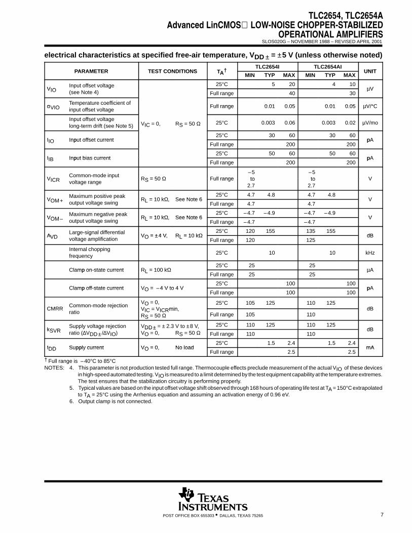
electrical characteristics at specified free-air temperature, VDD± = ±5 V (unless otherwise noted)
PARAMETER TEST CONDITIONS TA†TLC2654C TLC2654AC
UNITPARAMETER TEST CONDITIONS TA†MIN TYP MAX MIN TYP MAX
UNIT
VIOInput offset voltage 25°C 5 20 4 10
µVVIOg
(see Note 4) Full range 34 24µV
αVIOTemperature coefficient of
Full range 0 01 0 05 0 01 0 05 µV/°CαVIO input offset voltageFull range 0.01 0.05 0.01 0.05 µV/°C
Input offset voltage long-term drift (see Note 5) VIC = 0, RS = 50 Ω 25°C 0.003 0.06 0.003 0.02 µV/mo
IIO Input offset current25°C 30 60 30 60
pAIIO Input offset currentFull range 150 150
pA
IIB Input bias current25°C 50 60 50 60
pAIIB Input bias currentFull range 150 150
pA
VICRCommon-mode input
RS = 50 Ω Full range–5to
–5to VVICR voltage range
RS = 50 Ω Full range to2.7
to2.7
V
VOMMaximum positive peak
RL = 10 kΩ See Note 625°C 4.7 4.8 4.7 4.8
VVOM+ output voltage swingRL = 10 kΩ, See Note 6
Full range 4.7 4.7V
VOMMaximum negative peak
RL = 10 kΩ See Note 625°C –4.7 –4.9 –4.7 –4.9
VVOM–g
output voltage swingRL = 10 kΩ, See Note 6
Full range –4.7 –4.7V
AVDLarge-signal differential
VO = ±4 V RL = 10 kΩ25°C 120 155 135 155
dBAVDg g
voltage amplificationVO = ±4 V, RL = 10 kΩ
Full range 120 130dB
Internal choppingfrequency
25°C 10 10 kHz
Clamp on state current RL = 100 kΩ25°C 25 25
µAClamp on-state current RL = 100 kΩFull range 25 25
µA
Clamp off state current VO = 4 V to 4 V25°C 100 100
pAClamp off-state current VO = –4 V to 4 VFull range 100 100
pA
CMRRCommon-mode rejection
VO = 0,VIC VICRmin
25°C 105 125 110 125dBCMRR
jratio
VIC = VICRmin, RS = 50 Ω Full range 105 110
dB
kSVRSupply voltage rejection VDD± = ±2.3 V to ±8 V, 25°C 110 125 110 125
dBkSVRy g j
ratio (∆VDD± /∆VIO)DD± ,
VO = 0, RS = 50 Ω Full range 110 110dB
IDD Supply current VO = 0 No load25°C 1.5 2.4 1.5 2.4
mAIDD Supply current VO = 0, No loadFull range 2.5 2.5
mA
† Full range is 0°C to 70°C.NOTES: 4. This parameter is not production tested full range. Thermocouple effects preclude measurement of the actual VIO of these devices
in high-speed automated testing. VIO is measured to a limit determined by the test equipment capability at the temperature extremes.The test ensures that the stabilization circuitry is performing properly.
5. Typical values are based on the input offset voltage shift observed through 168 hours of operating life test at TA = 150°C extrapolatedto TA = 25° using the Arrhenius equation and assuming an activation energy of 0.96 eV.
6. Output clamp is not connected.

TLC2654, TLC2654AAdvanced LinCMOS LOW-NOISE CHOPPER-STABILIZEDOPERATIONAL AMPLIFIERS
SLOS020G – NOVEMBER 1988 – REVISED APRIL 2001
6 POST OFFICE BOX 655303 • DALLAS, TEXAS 75265
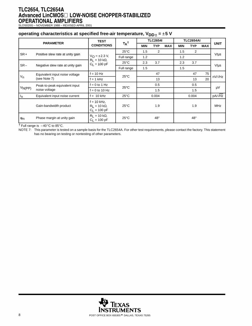
operating characteristics at specified free-air temperature, VDD± = ±5 V
PARAMETER TEST TA†TLC2654C TLC2654AC
UNITPARAMETER TESTCONDITIONS TA†
MIN TYP MAX MIN TYP MAXUNIT
SR+ Positive slew rate at unity gain25°C 1.5 2 1.5 2
V/µsSR+ Positive slew rate at unity gain VO = ±2.3 V,RL 10 kΩ
Full range 1.3 1.3V/µs
SR Negative slew rate at unity gain
RL = 10 kΩ,CL = 100 pF 25°C 2.3 3.7 2.3 3.7
V/µsSR– Negative slew rate at unity gain CL = 100 FFull range 1.7 1.7
V/µs
VEquivalent input noise voltage f = 10 Hz
25°C47 47 75
nV/√HzVnq g
(see Note 7) f = 1 kHz25°C
13 13 20nV/√Hz
VN(PP)Peak-to-peak equivalent input f = 0 to 1 Hz
25°C0.5 0.5
µVVN(PP)q
noise voltage f = 0 to 10 Hz25°C
1.5 1.5µV
In Equivalent input noise current f = 10 kHz 25°C 0.004 0.004 pA/√Hz
f = 10 kHz,Gain-bandwidth product
,RL = 10 kΩ, 25°C 1.9 1.9 MHzLCL = 100 pF
φm Phase margin at unity gainRL = 10 kΩ,CL = 100 pF
25°C 48° 48°
† Full range is 0°C to 70°C.NOTE 7: This parameter is tested on a sample basis for the TLC2654A. For other test requirements, please contact the factory. This statement
has no bearing on testing or nontesting of other parameters.
TLC2654, TLC2654AAdvanced LinCMOS LOW-NOISE CHOPPER-STABILIZED
OPERATIONAL AMPLIFIERS
SLOS020G – NOVEMBER 1988 – REVISED APRIL 2001
7POST OFFICE BOX 655303 • DALLAS, TEXAS 75265
electrical characteristics at specified free-air temperature, VDD ± = ±5 V (unless otherwise noted)
PARAMETER TEST CONDITIONS TA†TLC2654I TLC2654AI
UNITPARAMETER TEST CONDITIONS TA†MIN TYP MAX MIN TYP MAX
UNIT
VIOInput offset voltage 25°C 5 20 4 10
µVVIOg
(see Note 4) Full range 40 30µV
αVIOTemperature coefficient of
Full range 0 01 0 05 0 01 0 05 µV/°CαVIO input offset voltageFull range 0.01 0.05 0.01 0.05 µV/°C
Input offset voltage long-term drift (see Note 5) VIC = 0, RS = 50 Ω 25°C 0.003 0.06 0.003 0.02 µV/mo
IIO Input offset current25°C 30 60 30 60
pAIIO Input offset currentFull range 200 200
pA
IIB Input bias current25°C 50 60 50 60
pAIIB Input bias currentFull range 200 200
pA
VICRCommon-mode input
RS = 50 Ω Full range–5to
–5to VVICR voltage range
RS = 50 Ω Full range to2.7
to2.7
V
VOMMaximum positive peak
RL = 10 kΩ See Note 625°C 4.7 4.8 4.7 4.8
VVOM+ output voltage swingRL = 10 kΩ, See Note 6
Full range 4.7 4.7V
VOMMaximum negative peak
RL = 10 kΩ See Note 625°C –4.7 –4.9 –4.7 –4.9
VVOM–g
output voltage swingRL = 10 kΩ, See Note 6
Full range –4.7 –4.7V
AVDLarge-signal differential
VO = ±4 V RL = 10 kΩ25°C 120 155 135 155
dBAVDg g
voltage amplificationVO = ±4 V, RL = 10 kΩ
Full range 120 125dB
Internal choppingfrequency
25°C 10 10 kHz
Clamp on state current RL = 100 kΩ25°C 25 25
µAClamp on-state current RL = 100 kΩFull range 25 25
µA
Clamp off state current VO = 4 V to 4 V25°C 100 100
pAClamp off-state current VO = –4 V to 4 VFull range 100 100
pA
CMRRCommon-mode rejection
VO = 0,VIC VICRmin
25°C 105 125 110 125dBCMRR
jratio
VIC = VICRmin,RS = 50 Ω Full range 105 110
dB
kSVRSupply voltage rejection VDD± = ± 2.3 V to ±8 V, 25°C 110 125 110 125
dBkSVRy g j
ratio (∆VDD± /∆VIO)DD± ,
VO = 0, RS = 50 Ω Full range 110 110dB
IDD Supply current VO = 0 No load25°C 1.5 2.4 1.5 2.4
mAIDD Supply current VO = 0, No loadFull range 2.5 2.5
mA
† Full range is –40°C to 85°CNOTES: 4. This parameter is not production tested full range. Thermocouple effects preclude measurement of the actual VIO of these devices
in high-speed automated testing. VIO is measured to a limit determined by the test equipment capability at the temperature extremes.The test ensures that the stabilization circuitry is performing properly.
5. Typical values are based on the input offset voltage shift observed through 168 hours of operating life test at TA = 150°C extrapolatedto TA = 25°C using the Arrhenius equation and assuming an activation energy of 0.96 eV.
6. Output clamp is not connected.
TLC2654, TLC2654AAdvanced LinCMOS LOW-NOISE CHOPPER-STABILIZEDOPERATIONAL AMPLIFIERS
SLOS020G – NOVEMBER 1988 – REVISED APRIL 2001
8 POST OFFICE BOX 655303 • DALLAS, TEXAS 75265
operating characteristics at specified free-air temperature, VDD± = ±5 V
PARAMETERTEST
TA†TLC2654I TLC2654AI
UNITPARAMETERCONDITIONS TA†
MIN TYP MAX MIN TYP MAXUNIT
SR+ Positive slew rate at unity gain25°C 1.5 2 1.5 2
V/µsSR+ Positive slew rate at unity gain VO = ±2.3 V,RL 10 kΩ
Full range 1.2 1.2V/µs
SR Negative slew rate at unity gain
RL = 10 kΩ,CL = 100 pF 25°C 2.3 3.7 2.3 3.7
V/µsSR– Negative slew rate at unity gain CL = 100 FFull range 1.5 1.5
V/µs
VEquivalent input noise voltage f = 10 Hz
25°C47 47 75
nV/√HzVnq g
(see Note 7) f = 1 kHz25°C
13 13 20nV/√Hz
VN(PP)Peak-to-peak equivalent input f = 0 to 1 Hz
25°C0.5 0.5
µVVN(PP)q
noise voltage f = 0 to 10 Hz25°C
1.5 1.5µV
In Equivalent input noise current f = 10 kHz 25°C 0.004 0.004 pA/√Hz
f = 10 kHz,Gain-bandwidth product
f 10 kHz,RL = 10 kΩ, 25°C 1.9 1.9 MHzLCL = 100 pF
φm Phase margin at unity gainRL = 10 kΩ,CL = 100 pF
25°C 48° 48°
† Full range is –40 °C to 85°C.NOTE 7: This parameter is tested on a sample basis for the TLC2654A. For other test requirements, please contact the factory. This statement
has no bearing on testing or nontesting of other parameters.

TLC2654, TLC2654AAdvanced LinCMOS LOW-NOISE CHOPPER-STABILIZED
OPERATIONAL AMPLIFIERS
SLOS020G – NOVEMBER 1988 – REVISED APRIL 2001
9POST OFFICE BOX 655303 • DALLAS, TEXAS 75265
electrical characteristics at specified free-air temperature, VDD ± = ±5 V (unless otherwise noted)
PARAMETER TEST CONDITIONS TA†TLC2654QTLC2654M
TLC2654AQTLC2654AM UNITTA
MIN TYP MAX MIN TYP MAX
VIOInput offset voltage 25°C 5 20 4 10
µVVIOg
(see Note 4) Full range 50 40µV
αVIOTemperature coefficient of
Full range 0 01 0 05∗ 0 01 0 05∗ µV/°CαVIO input offset voltageFull range 0.01 0.05∗ 0.01 0.05∗ µV/°C
Input offset voltagelong-term drift (see Note 5) VIC = 0, RS = 50 Ω 25°C 0.003 0.06∗ 0.003 0.02∗ µV/mo
IIO Input offset current25°C 30 60 30 60
pAIIO Input offset currentFull range 500 500
pA
IIB Input bias current25°C 50 60 50 60
pAIIB Input bias currentFull range 500 500
pA
Common mode input–5 –5
VICRCommon-mode input voltage range
RS = 50 Ω Full range5to
5to VICR voltage range S g
2.7 2.7
VOMMaximum positive peak
RL = 10 kΩ See Note 625°C 4.7 4.8 4.7 4.8
VVOM+ output voltage swingRL = 10 kΩ, See Note 6
Full range 4.7 4.7V
VOMMaximum negative peak
RL = 10 kΩ See Note 625°C –4.7 –4.9 –4.7 –4.9
VVOM–g
output voltage swingRL = 10 kΩ, See Note 6
Full range –4.7 –4.7V
AVDLarge-signal differential
VO = ±4 V RL = 10 kΩ25°C 120 155 135 155
dBAVDg g
voltage amplificationVO = ±4 V, RL = 10 kΩ
Full range 120 120dB
Internal chopping frequency
25°C 10 10 kHz
Clamp on state current RL = 100 kΩ25°C 25 25
µAClamp on-state current RL = 100 kΩFull range 25 25
µA
Clamp off state current VO = 4 V to 4 V25°C 100 100
pAClamp off-state current VO = –4 V to 4 VFull range 500 500
pA
CMRRCommon-mode rejection
VO = 0,VIC VICRmin
25°C 105 125 110 125dBCMRR
jratio
VIC = VICRmin,RS = 50 Ω Full range 105 110
dB
kSVRSupply voltage rejection VDD± = ±2.3 V to ±8 V, 25°C 110 125 110 125
dBkSVRy g j
ratio (∆VDD± /∆VIO)DD± ,
VO = 0, RS = 50 Ω Full range 105 110dB
IDD Supply current VO = 0 No load25°C 1.5 2.4 1.5 2.4
mAIDD Supply current VO = 0, No loadFull range 2.5 2.5
mA
∗ On products complaint to MIL-STD-883, Class B, this parameter is not production tested.† Full range is –40° to 125°C for Q suffix, –55° to 125°C for M suffix.NOTES: 4. This parameter is not production tested full range. Thermocouple effects preclude measurement of the actual VIO of these devices
in high-speed automated testing. VIO is measured to a limit determined by the test equipment capability at the temperature extremes.The test ensures that the stabilization circuitry is performing properly.
5. Typical values are based on the input offset voltage shift observed through 168 hours of operating life test at TA = 150°C extrapolatedto TA = 25°C using the Arrhenius equation and assuming an activation energy of 0.96 eV.
6. Output clamp is not connected.

TLC2654, TLC2654AAdvanced LinCMOS LOW-NOISE CHOPPER-STABILIZEDOPERATIONAL AMPLIFIERS
SLOS020G – NOVEMBER 1988 – REVISED APRIL 2001
10 POST OFFICE BOX 655303 • DALLAS, TEXAS 75265
operating characteristics at specified free-air temperature, VDD± = ±5 V
PARAMETER TEST CONDITIONS TA†
TLC2654QTLC2654MTLC2654AQTLC2654AM
UNIT
MIN TYP MAX
SR+ Positive slew rate at unity gain25°C 1.5 2
V/µsSR+ Positive slew rate at unity gain
VO = ±2 3 V RL = 10 kΩ CL = 100 pFFull range 1.1
V/µs
SR Negative slew rate at unity gain
VO = ±2.3 V, RL = 10 kΩ, CL = 100 pF25°C 2.3 3.7
V/µsSR– Negative slew rate at unity gainFull range 1.3
V/µs
V Equivalent input noise voltagef = 10 Hz 25°C 47
nV/√HzVn Equivalent input noise voltagef = 1 kHz 25°C 13
nV/√Hz
VN(PP)Peak-to-peak equivalent input f = 0 to 1 Hz 25°C 0.5
µVVN(PP)q
noise voltage f = 0 to 10 Hz 25°C 1.5µV
In Equivalent input noise current f = 1 kHz 25°C 0.004 pA/√Hz
Gain-bandwidth product f = 10 kHz, RL = 10 kΩ, CL = 100 pF 25°C 1.9 MHz
φm Phase margin at unity gain RL = 10 kΩ, CL = 100 pF 25°C 48°† Full range is –40° to 125°C for Q suffix, –55° to 125°C for M suffix.
TLC2654, TLC2654AAdvanced LinCMOS LOW-NOISE CHOPPER-STABILIZED
OPERATIONAL AMPLIFIERS
SLOS020G – NOVEMBER 1988 – REVISED APRIL 2001
11POST OFFICE BOX 655303 • DALLAS, TEXAS 75265
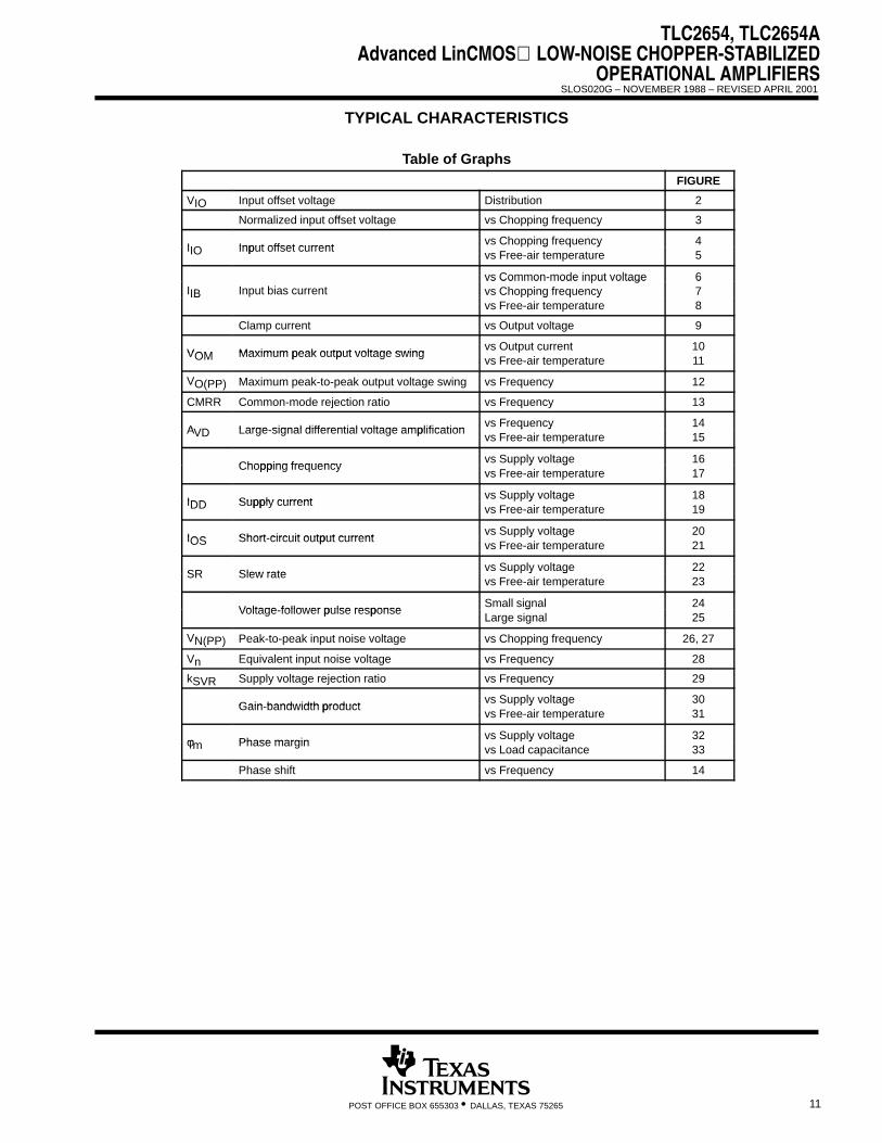
TYPICAL CHARACTERISTICS
Table of GraphsFIGURE
VIO Input offset voltage Distribution 2
Normalized input offset voltage vs Chopping frequency 3
IIO Input offset currentvs Chopping frequency 4
IIO Input offset currentg q y
vs Free-air temperature 5
vs Common-mode input voltage 6IIB Input bias current
vs Common mode in ut voltagevs Chopping frequency
67IB g q y
vs Free-air temperature 8
Clamp current vs Output voltage 9
VOM Maximum peak output voltage swingvs Output current 10
VOM Maximum peak output voltage swingvs Free-air temperature 11
VO(PP) Maximum peak-to-peak output voltage swing vs Frequency 12
CMRR Common-mode rejection ratio vs Frequency 13
AVD Large signal differential voltage amplificationvs Frequency 14
AVD Large-signal differential voltage amplificationq y
vs Free-air temperature 15
Chopping frequencyvs Supply voltage 16
Chopping frequencyy g
vs Free-air temperature 17
IDD Supply currentvs Supply voltage 18
IDD Supply currenty g
vs Free-air temperature 19
IOS Short circuit output currentvs Supply voltage 20
IOS Short-circuit output currenty g
vs Free-air temperature 21
SR Slew ratevs Supply voltage 22
SR Slew ratey g
vs Free-air temperature 23
Voltage follower pulse responseSmall signal 24
Voltage-follower pulse responseg
Large signal 25
VN(PP) Peak-to-peak input noise voltage vs Chopping frequency 26, 27
Vn Equivalent input noise voltage vs Frequency 28
kSVR Supply voltage rejection ratio vs Frequency 29
Gain bandwidth productvs Supply voltage 30
Gain-bandwidth producty g
vs Free-air temperature 31
φ Phase marginvs Supply voltage 32φm Phase margin
y gvs Load capacitance 33
Phase shift vs Frequency 14

TLC2654, TLC2654AAdvanced LinCMOS LOW-NOISE CHOPPER-STABILIZEDOPERATIONAL AMPLIFIERS
SLOS020G – NOVEMBER 1988 – REVISED APRIL 2001
12 POST OFFICE BOX 655303 • DALLAS, TEXAS 75265
TYPICAL CHARACTERISTICS†
Figure 2
8
4
0
Per
cen
tag
e o
f U
nit
s –
%
12
16
DISTRIBUTION OF TLC2654INPUT OFFSET VOLTAGE
20
–20 –16 –12 – 8 – 4 0 4 8 12 16 20
456 Units Tested From 4 Wafer Lots
VIO – Input Offset Voltage – µV
VDD± = ±5 VTA = 25°CN Package
Figure 3
10
0
–10
VIO
– N
orm
aliz
ed In
pu
t O
ffse
t V
olt
age
– u
V
20
30
NORMALIZED INPUT OFFSET VOLTAGEvs
CHOPPING FREQUENCY40
100 1K 10K 100K
VIO
µV
VDD± = ± 5 VVIC = 0TA = 25°C
Chopping Frequency – Hz
Figure 4
60
40
20
0100 1 k 10 k
IIO –
Inp
ut
Off
set
Cu
rren
t –
pA
80
INPUT OFFSET CURRENTvs
CHOPPING FREQUENCY
100
100 k
I IO
120
140VDD± = ±5 VVIC = 0TA = 25°C
Chopping Frequency – Hz
Figure 5
IIO –
Inp
ut
Off
set
Cu
rren
t –
pA
I IO
60
40
20
025 45 65 85
80
INPUT OFFSET CURRENTvs
FREE-AIR TEMPERATURE100
105 125
TA – Free-Air Temperature – °C
VDD± = ±5 VVIC = 0
†Data at high and low temperatures are applicable only within the rated operating free-air temperature ranges of the various devices.

TLC2654, TLC2654AAdvanced LinCMOS LOW-NOISE CHOPPER-STABILIZED
OPERATIONAL AMPLIFIERS
SLOS020G – NOVEMBER 1988 – REVISED APRIL 2001
13POST OFFICE BOX 655303 • DALLAS, TEXAS 75265
TYPICAL CHARACTERISTICS†
Figure 6
VIC – Common-Mode Input Voltage – V
INPUT BIAS CURRENTvs
COMMON-MODE INPUT VOLTAGE
10
IIB –
Inp
ut
Bia
s C
urr
ent
– p
A
100
1000
– 5 – 3 –1 1 3 5
I IB
VDD± = ±5 VTA = 25°C
– 4 – 2 0 2 4
Figure 7
INPUT BIAS CURRENTvs
CHOPPING FREQUENCY
60
40
20
0100 1 k 10 k 100 k
IIB –
Inp
ut
Bia
s C
urr
ent
– p
A
80
100
I IB
VDD± = ±5 VVIC = 0TA = 25°C
Chopping Frequency – Hz
Figure 8
TA – Free-Air Temperature – °C
60
40
20
025 45 65 85
IIB –
Inp
ut
Bia
s C
urr
ent
– p
A
80
INPUT BIAS CURRENTvs
FREE-AIR TEMPERATURE100
105 125
I IB
VDD± = ±5 VVIC = 0
Figure 9
1 nA
100 pA
10 pA
1 pA4 4.2 4.4 4.6
|Cla
mp
Cu
rren
t|
10
CLAMP CURRENTvs
OUTPUT VOLTAGE
4.8 5|VO| – Output Voltage – V
1
100 nA
10 nA
VDD± = ±5 VTA = 25°C
100 Aµ
Aµ
Aµ
Positive Clamp Current
Negative Clamp Current
†Data at high and low temperatures are applicable only within the rated operating free-air temperature ranges of the various devices.
TLC2654, TLC2654AAdvanced LinCMOS LOW-NOISE CHOPPER-STABILIZEDOPERATIONAL AMPLIFIERS
SLOS020G – NOVEMBER 1988 – REVISED APRIL 2001
14 POST OFFICE BOX 655303 • DALLAS, TEXAS 75265
TYPICAL CHARACTERISTICS†
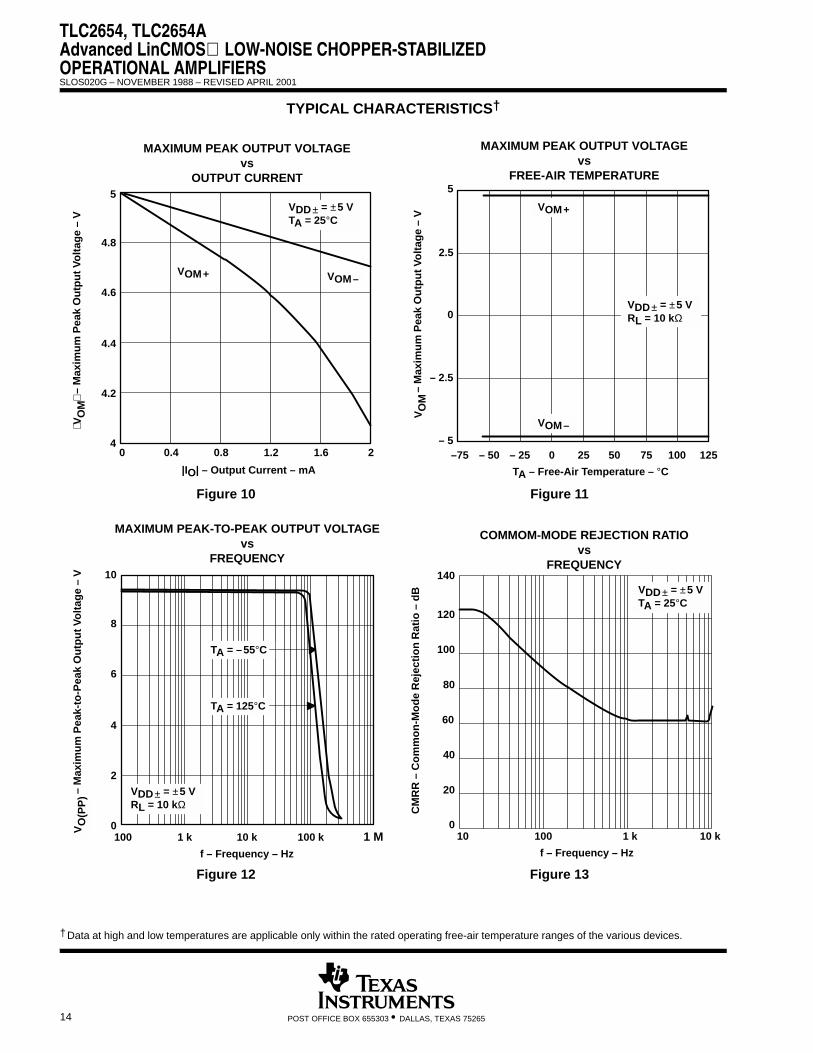
Figure 10
4.6
4.4
4.2
4
– M
axim
um
Pea
k O
utp
ut
Vo
ltag
e –
V
4.8
MAXIMUM PEAK OUTPUT VOLTAGEvs
OUTPUT CURRENT5
O
M
|IO| – Output Current – mA
VDD± = ±5 VTA = 25°C
VOM+ VOM–
0 0.4 0.8 1.2 1.6 2
V
Figure 11
TA – Free-Air Temperature – °C
5
0
– 2.5
– 5–75 – 50 – 25 0 25 50
MAXIMUM PEAK OUTPUT VOLTAGEvs
FREE-AIR TEMPERATURE
75 100 125
2.5
VDD± = ±5 VRL = 10 kΩ
– M
axim
um
Pea
k O
utp
ut
Vo
ltag
e –
V O
MV
VOM+
VOM–
Figure 12
6
4
2
0VO
(PP
) –
Max
imu
m P
eak-
to-P
eak
Ou
tpu
t V
olt
age
– V
8
10
100 1 k 10 k
f – Frequency – Hz
MAXIMUM PEAK-TO-PEAK OUTPUT VOLTAGEvs
FREQUENCY
100 k 1 M
VO
(PP
)
TA = –55°C
TA = 125°C
VDD± = ±5 VRL = 10 kΩ
Figure 13
100
80
40
20
0
140
60
10 100 1 k 10 k
CM
RR
– C
om
mo
n-M
od
e R
ejec
tio
n R
atio
– d
B
120
f – Frequency – Hz
COMMOM-MODE REJECTION RATIOvs
FREQUENCY
VDD± = ±5 VTA = 25°C
†Data at high and low temperatures are applicable only within the rated operating free-air temperature ranges of the various devices.
TLC2654, TLC2654AAdvanced LinCMOS LOW-NOISE CHOPPER-STABILIZED
OPERATIONAL AMPLIFIERS
SLOS020G – NOVEMBER 1988 – REVISED APRIL 2001
15POST OFFICE BOX 655303 • DALLAS, TEXAS 75265
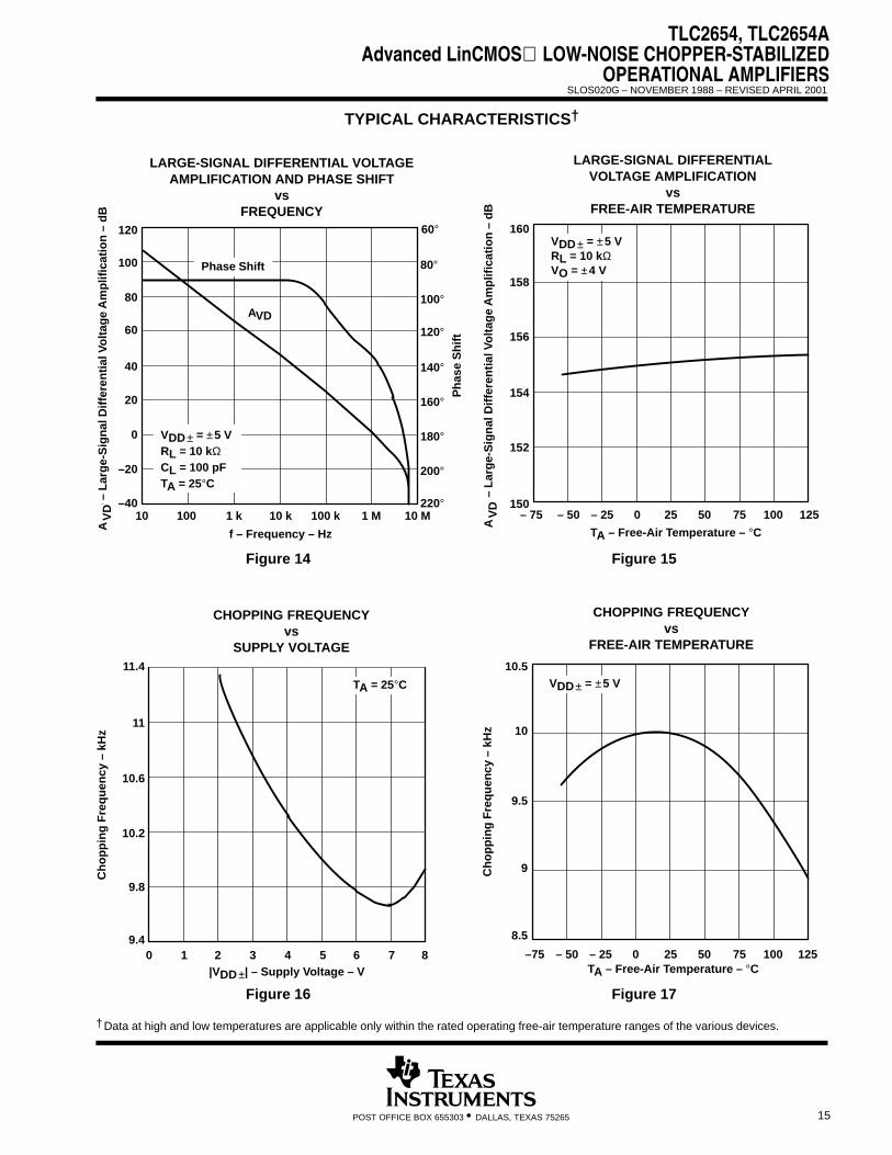
TYPICAL CHARACTERISTICS†
Figure 14
20
0
–20
–40
AV
D –
Lar
ge-
Sig
nal
Dif
fere
nti
al V
olt
age
Am
plif
icat
ion
– d
B
40
60
80
10 100 1 k 10 k 100 k
f – Frequency – Hz
LARGE-SIGNAL DIFFERENTIAL VOLTAGEAMPLIFICATION AND PHASE SHIFT
vsFREQUENCY
1 M 10 M
100
120
220°
200°
180°
160°
140°
120°
100°
80°
60°
AV
D
VDD± = ±5 VRL = 10 kΩCL = 100 pFTA = 25°C
Phase Shift
AVD
Ph
ase
Sh
ift
Figure 15
TA – Free-Air Temperature – °C
156
154
152
– 25 0 50
158
LARGE-SIGNAL DIFFERENTIALVOLTAGE AMPLIFICATION
vsFREE-AIR TEMPERATURE
160
100 125– 50 25 75
VDD± = ±5 VRL = 10 kΩVO = ±4 V
AV
D –
Lar
ge-
Sig
nal
Dif
fere
nti
al V
olt
age
Am
plif
icat
ion
– d
BA
VD
– 75150
Figure 16
|VDD±| – Supply Voltage – V
10.6
10.2
9.8
9.40 1 2 3 4 5
Ch
op
pin
g F
req
uen
cy –
kH
z
11
11.4
CHOPPING FREQUENCYvs
SUPPLY VOLTAGE
6 7 8
TA = 25°C
Figure 17
10.5
9.5
9
8.5
–75 – 50 – 25 0 25 50
CHOPPING FREQUENCYvs
FREE-AIR TEMPERATURE
75 100 125
10
VDD± = ±5 V
TA – Free-Air Temperature – °C
Ch
op
pin
g F
req
uen
cy –
kH
z
†Data at high and low temperatures are applicable only within the rated operating free-air temperature ranges of the various devices.
TLC2654, TLC2654AAdvanced LinCMOS LOW-NOISE CHOPPER-STABILIZEDOPERATIONAL AMPLIFIERS
SLOS020G – NOVEMBER 1988 – REVISED APRIL 2001
16 POST OFFICE BOX 655303 • DALLAS, TEXAS 75265
TYPICAL CHARACTERISTICS†
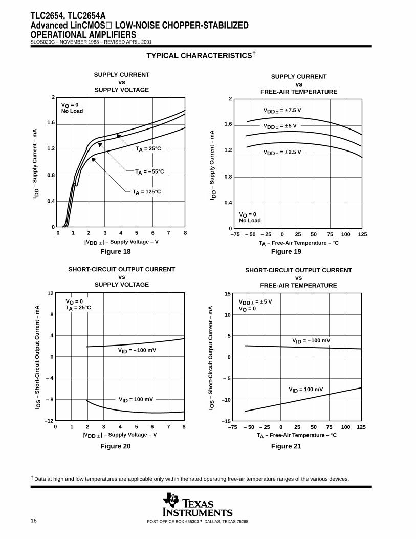
Figure 18
IDD
– S
up
ply
Cu
rren
t –
mA
I DD
1.2
0.8
0.4
00 2 3 5
1.6
SUPPLY CURRENTvs
SUPPLY VOLTAGE2
7 81 4 6
TA = 25°C
TA = –55°C
TA = 125°C
VO = 0No Load
|VDD ± | – Supply Voltage – V
Figure 19
1.2
0.8
0.4
0–75 – 25 0 50
IDD
– S
up
ply
Cu
rren
t –
mA
1.6
SUPPLY CURRENTvs
FREE-AIR TEMPERATURE2
100 125– 50 25 75
I DD
VDD± = ±5 V
VDD± = ±7.5 V
VDD± = ±2.5 V
VO = 0No Load
TA – Free-Air Temperature – °C
Figure 20
0
– 4
– 8
–120 1 2 3 4 5
IOS
– S
ho
rt-C
ircu
it O
utp
ut
Cu
rren
t –
mA
4
8
SHORT-CIRCUIT OUTPUT CURRENTvs
SUPPLY VOLTAGE12
6 7 8|VDD ± | – Supply Voltage – V
I OS
VO = 0TA = 25°C
VID = –100 mV
VID = 100 mV
Figure 21
0
– 5
–10
–15–75 – 50 – 25 0 25 50
IOS
– S
ho
rt-C
ircu
it O
utp
ut
Cu
rren
t –
mA
5
10
SHORT-CIRCUIT OUTPUT CURRENTvs
FREE-AIR TEMPERATURE15
75 100 125TA – Free-Air Temperature – °C
I OS
VID = 100 mV
VID = –100 mV
VDD± = ±5 VVO = 0
†Data at high and low temperatures are applicable only within the rated operating free-air temperature ranges of the various devices.

TLC2654, TLC2654AAdvanced LinCMOS LOW-NOISE CHOPPER-STABILIZED
OPERATIONAL AMPLIFIERS
SLOS020G – NOVEMBER 1988 – REVISED APRIL 2001
17POST OFFICE BOX 655303 • DALLAS, TEXAS 75265
TYPICAL CHARACTERISTICS†
Figure 22
5
4
1
01 2 3 4 5 6 7
SR
– S
lew
Rat
e –
V/u
s
SLEW RATEvs
SUPPLY VOLTAGE
8
3
2
µs
V/
RL = 10 kΩCL = 100 pFTA = 25°C
SR–
0
|VDD ± | – Supply Voltage – V
SR+
Figure 23
1
0 25 50
SR
– S
lew
Rat
e –
V/u
s
3
SLEW RATEvs
FREE-AIR TEMPERATURE4
75 100 125
2
0µ
sV
/
VDD± = ±5 VRL = 10 kΩCL = 100 pF
SR–
SR+
–75 –50 –25
TA – Free-Air Temperature – °C
Figure 24
t – Time – µs
25
– 50
–75
–1000 1 2 3
VO
– O
utp
ut
Vo
ltag
e –
mV
75
VOLTAGE-FOLLOWERSMALL-SIGNAL
PULSE RESPONSE
4 6
0
100
50
– 25
VO
VDD± = ±5 VRL = 10 kΩCL = 100 pFTA = 25°C
5 7
Figure 25t – Time – µs
5 10 15 20 25 30
VO
– O
utp
ut
Vo
ltag
e –
V
VOLTAGE-FOLLOWERLARGE-SIGNAL
PULSE RESPONSE
35 40
VO
VDD± = ±5 VRL = 10 kΩCL = 100 pFTA = 25°C
1
– 2
– 3
– 4
3
0
4
2
–1
0
†Data at high and low temperatures are applicable only within the rated operating free-air temperature ranges of the various devices.
TLC2654, TLC2654AAdvanced LinCMOS LOW-NOISE CHOPPER-STABILIZEDOPERATIONAL AMPLIFIERS
SLOS020G – NOVEMBER 1988 – REVISED APRIL 2001
18 POST OFFICE BOX 655303 • DALLAS, TEXAS 75265
TYPICAL CHARACTERISTICS
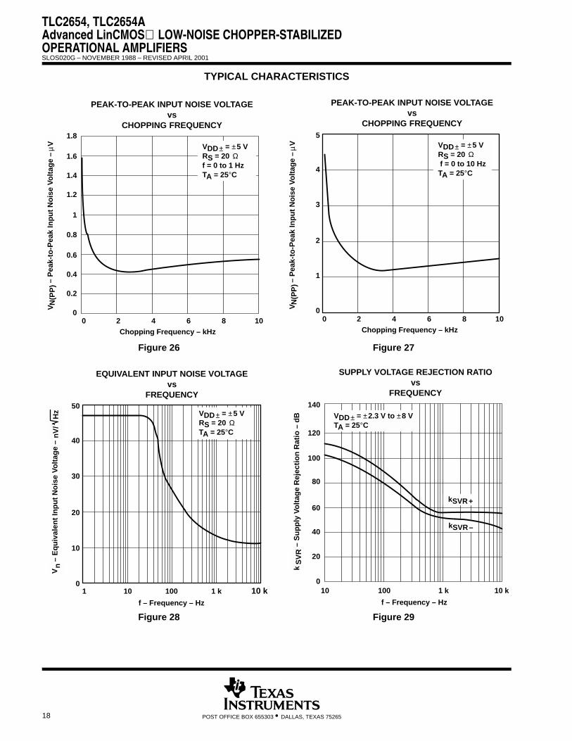
Figure 26
Chopping Frequency – kHz
VN
(PP
) –
Pea
k-to
-Pea
k In
pu
t N
ois
e V
olt
age
– u
VN
(PP
)V
PEAK-TO-PEAK INPUT NOISE VOLTAGEvs
CHOPPING FREQUENCY
0
0.2
0.4
0.6
0.8
1
1.2
1.4
1.6
1.8
0 2 4 6 8 10
VDD± = ±5 VRS = 20 Ωf = 0 to 1 HzTA = 25°C
µV
Figure 27
VN
(PP
) –
Pea
k-to
-Pea
k In
pu
t N
ois
e V
olt
age
– u
VN
(PP
)V
µV
3
2
1
00 2 4 6
4
PEAK-TO-PEAK INPUT NOISE VOLTAGEvs
CHOPPING FREQUENCY5
8 10
VDD± = ±5 VRS = 20 Ω f = 0 to 10 HzTA = 25°C
Chopping Frequency – kHz
Figure 28
30
20
10
01 10 100
VN
– E
qu
ival
ent
Inp
ut
No
ise
Vo
ltag
e –
xxxx
xx
40
f – Frequency – Hz
EQUIVALENT INPUT NOISE VOLTAGEvs
FREQUENCY50
1 k 10 k
nV
/H
zV
n
VDD± = ±5 VRS = 20 Ω TA = 25°C
Figure 29
100
80
40
20
140
60
100 1 k 10 k
kSV
R –
Su
pp
ly V
olt
age
Rej
ecti
on
Rat
io –
dB
120
f – Frequency – Hz
SUPPLY VOLTAGE REJECTION RATIOvs
FREQUENCY
k S
VR
VDD± = ±2.3 V to ±8 VTA = 25°C
kSVR+
kSVR–
010
TLC2654, TLC2654AAdvanced LinCMOS LOW-NOISE CHOPPER-STABILIZED
OPERATIONAL AMPLIFIERS
SLOS020G – NOVEMBER 1988 – REVISED APRIL 2001
19POST OFFICE BOX 655303 • DALLAS, TEXAS 75265
TYPICAL CHARACTERISTICS†
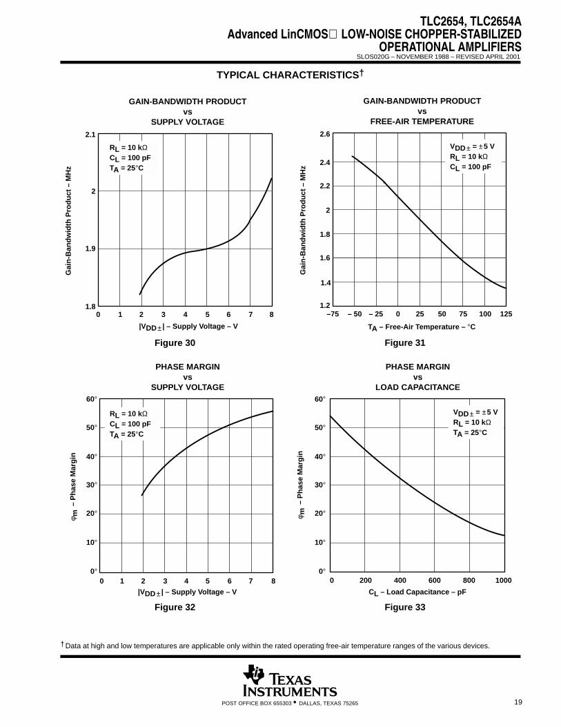
Figure 30
|VDD± | – Supply Voltage – V
1.9
1.80 1 2 3 4 5
Gai
n-B
and
wid
th P
rod
uct
– M
Hz
2
GAIN-BANDWIDTH PRODUCTvs
SUPPLY VOLTAGE2.1
6 7 8
RL = 10 kΩCL = 100 pFTA = 25°C
Figure 31
2
1.8
1.6
1.2–75 – 50 – 25 0 25 50
Gai
n-B
and
wid
th P
rod
uct
– M
Hz
2.2
2.4
GAIN-BANDWIDTH PRODUCTvs
FREE-AIR TEMPERATURE
2.6
75 100 125
VDD± = ±5 VRL = 10 kΩCL = 100 pF
1.4
TA – Free-Air Temperature – °C
Figure 32
0 2 3 5
– P
has
e M
arg
in
PHASE MARGINvs
SUPPLY VOLTAGE
7 81 4 6
φ m
|VDD± | – Supply Voltage – V
60°
50°
40°
30°
20°
10°
0°
RL = 10 kΩCL = 100 pFTA = 25°C
Figure 33
60°
50°
40°
30°
20°
10°
0°
CL – Load Capacitance – pF
0 200 400 600
PHASE MARGINvs
LOAD CAPACITANCE
800 1000
VDD± = ±5 VRL = 10 kΩTA = 25°C
– P
has
e M
arg
inφ m
†Data at high and low temperatures are applicable only within the rated operating free-air temperature ranges of the various devices.
0
– 500 10 20 30 40
VI –
Inp
ut
Vo
ltag
e –
mV
V
O –
Ou
tpu
t V
olt
age
– V
– 5
t – Time – ms
0
50 60 70 80
VI
VO
VDD± = ±5 VTA = 25°C
Figure 34. Overload Recovery
TLC2654, TLC2654AAdvanced LinCMOS LOW-NOISE CHOPPER-STABILIZEDOPERATIONAL AMPLIFIERS
SLOS020G – NOVEMBER 1988 – REVISED APRIL 2001
20 POST OFFICE BOX 655303 • DALLAS, TEXAS 75265
APPLICATION INFORMATION
capacitor selection and placement
Leakage and dielectric absorption are the two important factors to consider when selecting external capacitorsCXA and CXB. Both factors can cause system degradation, negating the performance advantages realized byusing the TLC2654.
Degradation from capacitor leakage becomes more apparent with increasing temperatures. Low-leakagecapacitors and standoffs are recommended for operation at TA = 125°C. In addition, guard bands arerecommended around the capacitor connections on both sides of the printed-circuit board to alleviate problemscaused by surface leakage on circuit boards.
Capacitors with high dielectric absorption tend to take several seconds to settle upon application of power, whichdirectly affects input offset voltage. In applications needing fast settling of input voltage, high-quality filmcapacitors such as mylar, polystyrene, or polypropylene should be used. In other applications, a ceramic orother low-grade capacitor can suffice.
Unlike many choppers available today, the TLC2654 is designed to function with values of CXA and CXB in therange of 0.1 µF to 1 µF without degradation to input offset voltage or input noise voltage. These capacitorsshould be located as close as possible to CXA and CXB and return to either VDD– or C RETURN. On manychoppers, connecting these capacitors to VDD– causes degradation in noise performance; this problem iseliminated on the TLC2654.
internal/external clock
The TLC2654 has an internal clock that sets the chopping frequency to a nominal value of 10 kHz. On 8-pinpackages, the chopping frequency can only be controlled by the internal clock; however, on all 14-pin packagesand the 20-pin FK package the device chopping frequency can be set by the internal clock or controlledexternally by use of the INT/EXT and CLK IN. To use the internal 10-kHz clock, no connection is necessary. Ifexternal clocking is desired, connect INT/EXT to VDD– and the external clock to CLK IN. The external clock trippoint is 2.5 V above the negative rail; however, CLK IN can be driven from the negative rail to 5 V above thenegative rail. This allows the TLC2654 to be driven directly by 5-V TTL and CMOS logic when operating in thesingle-supply configuration. If this 5-V level is exceeded, damage could occur to the device unless the currentinto CLK IN is limited to ±5 mA. A divide-by-twofrequency divider interfaces with CLK IN and setsthe chopping frequency. The chopping frequencyappears on CLK OUT.
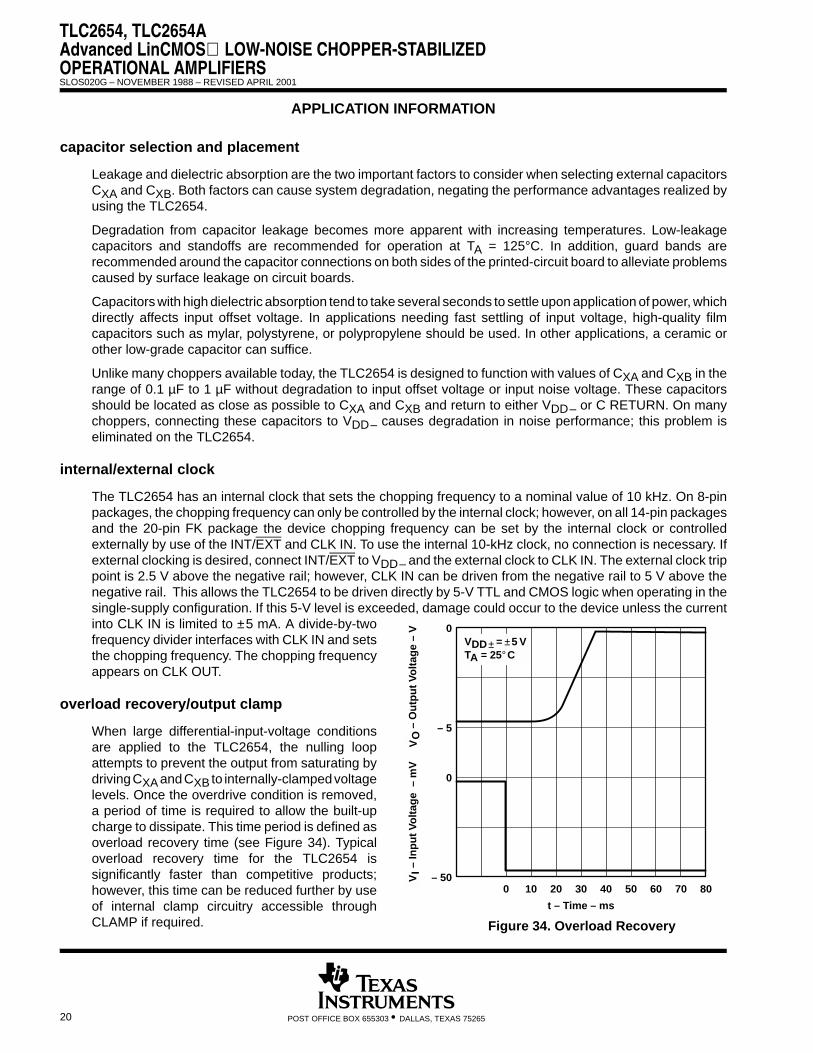
overload recovery/output clamp
When large differential-input-voltage conditionsare applied to the TLC2654, the nulling loopattempts to prevent the output from saturating bydriving CXA and CXB to internally-clamped voltagelevels. Once the overdrive condition is removed,a period of time is required to allow the built-upcharge to dissipate. This time period is defined asoverload recovery time (see Figure 34). Typicaloverload recovery time for the TLC2654 issignificantly faster than competitive products;however, this time can be reduced further by useof internal clamp circuitry accessible throughCLAMP if required.
TLC2654, TLC2654AAdvanced LinCMOS LOW-NOISE CHOPPER-STABILIZED
OPERATIONAL AMPLIFIERS
SLOS020G – NOVEMBER 1988 – REVISED APRIL 2001
21POST OFFICE BOX 655303 • DALLAS, TEXAS 75265
APPLICATION INFORMATION
overload recovery/output clamp (continued)
The clamp is a switch that is automatically activated when the output is approximately 1 V from either supplyrail. When connected to the inverting input (in parallel with the closed-loop feedback resistor), the closed-loopgain is reduced and the TLC2654 output is prevented from going into saturation. Since the output must sourceor sink current through the switch (see Figure 9), the maximum output voltage swing is slightly reduced.
thermoelectric effects
To take advantage of the extremely low offset voltage temperature coefficient of the TLC2654, care must betaken to compensate for the thermoelectric effects present when two dissimilar metals are brought into contactwith each other (such as device leads being soldered to a printed-circuit board). It is not uncommon for dissimilarmetal junctions to produce thermoelectric voltages in the range of several microvolts per degree Celsius (ordersof magnitude greater than the 0.01 µV/°C typical of the TLC2654).
To help minimize thermoelectric effects, pay careful attention to component selection and circuit-board layout.Avoid the use of nonsoldered connections (such as sockets, relays, switches, etc.) in the input signal path.Cancel thermoelectric effects by duplicating the number of components and junctions in each device input. Theuse of low-thermoelectric-coefficient components, such as wire-wound resistors, is also beneficial.
latch-up avoidance
Because CMOS devices are susceptible to latch-up due to their inherent parasitic thyristors, the TLC2654 inputsand outputs are designed to withstand –100-mA surge currents without sustaining latch-up; however,techniques to reduce the chance of latch-up should be used whenever possible. Internal protection diodesshould not, by design, be forward biased. Applied input and output voltages should not exceed the supplyvoltage by more than 300 mV. Care should be exercised when using capacitive coupling on pulse generators.Supply transients should be stunted by the use of decoupling capacitors (0.1 µF typical) located across thesupply rails as close to the device as possible.
The current path established if latch-up occurs is usually between the supply rails and is limited only by theimpedance of the power supply and the forward resistance of the parasitic thyristor. The chance of latch-upoccurring increases with increasing temperature and supply voltage.
electrostatic-discharge protection
The TLC2654 incorporates internal ESD-protection circuits that prevent functional failures at voltages at orbelow 2000 V. Care should be exercised in handling these devices, as exposure to ESD may result indegradation of the device parametric performance.
theory of operation
Chopper-stabilized operational amplifiers offer the best dc performance of any monolithic operational amplifier.This superior performance is the result of using two operational amplifiers — a main amplifier and a nullingamplifier – plus oscillator-controlled logic and two external capacitors to create a system that behaves as asingle amplifier. With this approach, the TLC2654 achieves submicrovolt input offset voltage, submicrovoltnoise voltage, and offset voltage variations with temperature in the nV/°C range.
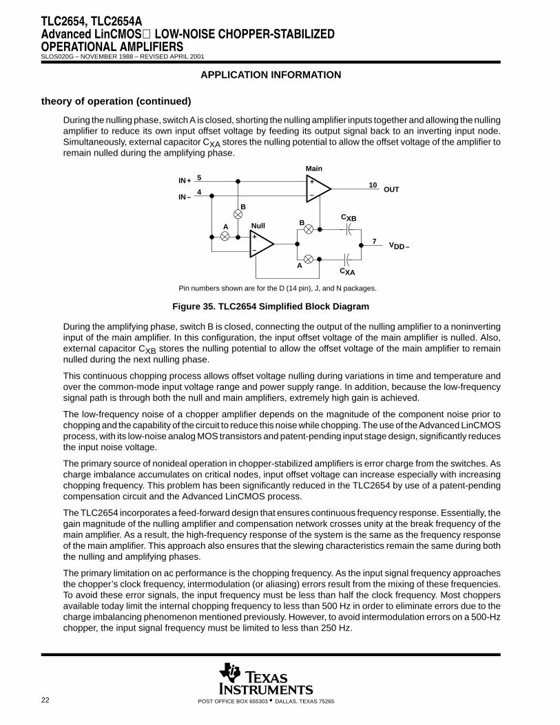
The TLC2654 on-chip control logic produces two dominant clock phases: a nulling phase and an amplifyingphase. The term chopper-stabilized derives from the process of switching between these two clock phases.Figure 35 shows a simplified block diagram of the TLC2654. Switches A and B are make-before-break types.
TLC2654, TLC2654AAdvanced LinCMOS LOW-NOISE CHOPPER-STABILIZEDOPERATIONAL AMPLIFIERS
SLOS020G – NOVEMBER 1988 – REVISED APRIL 2001
22 POST OFFICE BOX 655303 • DALLAS, TEXAS 75265
APPLICATION INFORMATION
theory of operation (continued)
During the nulling phase, switch A is closed, shorting the nulling amplifier inputs together and allowing the nullingamplifier to reduce its own input offset voltage by feeding its output signal back to an inverting input node.Simultaneously, external capacitor CXA stores the nulling potential to allow the offset voltage of the amplifier toremain nulled during the amplifying phase.
Null
IN+
IN–
Main
VDD–
CXA
CXBB
A
B
A+
+
–
–
5
410
OUT
7
Pin numbers shown are for the D (14 pin), J, and N packages.
Figure 35. TLC2654 Simplified Block Diagram
During the amplifying phase, switch B is closed, connecting the output of the nulling amplifier to a noninvertinginput of the main amplifier. In this configuration, the input offset voltage of the main amplifier is nulled. Also,external capacitor CXB stores the nulling potential to allow the offset voltage of the main amplifier to remainnulled during the next nulling phase.
This continuous chopping process allows offset voltage nulling during variations in time and temperature andover the common-mode input voltage range and power supply range. In addition, because the low-frequencysignal path is through both the null and main amplifiers, extremely high gain is achieved.
The low-frequency noise of a chopper amplifier depends on the magnitude of the component noise prior tochopping and the capability of the circuit to reduce this noise while chopping. The use of the Advanced LinCMOSprocess, with its low-noise analog MOS transistors and patent-pending input stage design, significantly reducesthe input noise voltage.
The primary source of nonideal operation in chopper-stabilized amplifiers is error charge from the switches. Ascharge imbalance accumulates on critical nodes, input offset voltage can increase especially with increasingchopping frequency. This problem has been significantly reduced in the TLC2654 by use of a patent-pendingcompensation circuit and the Advanced LinCMOS process.
The TLC2654 incorporates a feed-forward design that ensures continuous frequency response. Essentially, thegain magnitude of the nulling amplifier and compensation network crosses unity at the break frequency of themain amplifier. As a result, the high-frequency response of the system is the same as the frequency responseof the main amplifier. This approach also ensures that the slewing characteristics remain the same during boththe nulling and amplifying phases.
The primary limitation on ac performance is the chopping frequency. As the input signal frequency approachesthe chopper’s clock frequency, intermodulation (or aliasing) errors result from the mixing of these frequencies.To avoid these error signals, the input frequency must be less than half the clock frequency. Most choppersavailable today limit the internal chopping frequency to less than 500 Hz in order to eliminate errors due to thecharge imbalancing phenomenon mentioned previously. However, to avoid intermodulation errors on a 500-Hzchopper, the input signal frequency must be limited to less than 250 Hz.

TLC2654, TLC2654AAdvanced LinCMOS LOW-NOISE CHOPPER-STABILIZED
OPERATIONAL AMPLIFIERS
SLOS020G – NOVEMBER 1988 – REVISED APRIL 2001
23POST OFFICE BOX 655303 • DALLAS, TEXAS 75265
APPLICATION INFORMATION
theory of operation (continued)
The TLC2654 removes this restriction on ac performance by using a 10-kHz internal clock frequency. This highchopping frequency allows amplification of input signals up to 5 kHz without errors due to intermodulation andgreatly reduces low-frequency noise.
THERMAL INFORMATION
temperature coefficient of input offset voltage
Figure 36 shows the effects of package-included thermal EMF. The TLC2654 can null only the offset voltagewithin its nulling loop. There are metal-to-metal junctions outside the nulling loop (bonding wires, solder joints,etc.) that produce EMF. In Figure 36, a TLC2654 packaged in a 14-pin plastic package (N package) was placedin an oven at 25°C at t = 0, biased up, and allowed to stabilize. At t = 3 min, the oven was turned on and allowedto rise in temperature to 125°C. As evidenced by the curve, the overall change in input offset voltage withtemperature is less than the specified maximum limit of 0.05 µV/°C.
– In
pu
t O
ffse
t V
olt
age
–
– 12
– 15
4
– 180 3 6 9 12 15 18
– 4
– 8
0
t – Time – min
8
21 24 27 30
0.1 µF
0.1 µF
50 kΩ
5 V
–5 V
50 kΩ
100 Ω
VO
VIO = VO/1000
0
– 0.04
0.04
+
–
VIO
Vµ
aVIO
– T
emp
erat
ure
Co
effi
cien
t of
Inp
ut
Off
set
Vo
ltag
e –
uV
/C
αV
IOV
/µ
C°
IN–
IN+
4
5OUT
10– 0.08
– 0.12
– 0.16
– 0.2
0.08
Pin numbers shown are for the D (14-pin), J, and Npackages.
Figure 36. Effects of Package-Induced Thermal EMF
PACKAGE OPTION ADDENDUM
www.ti.com 14-Aug-2021
Addendum-Page 1
PACKAGING INFORMATION
Orderable Device Status(1)
Package Type PackageDrawing
Pins PackageQty
Eco Plan(2)
Lead finish/Ball material
(6)
MSL Peak Temp(3)
Op Temp (°C) Device Marking(4/5)
Samples
5962-9089504QPA ACTIVE CDIP JG 8 1 Non-RoHS& Green
SNPB N / A for Pkg Type -55 to 125 9089504QPATLC2654AM
TLC2654AC-8D ACTIVE SOIC D 8 75 RoHS & Green NIPDAU Level-1-260C-UNLIM 2654AC
TLC2654ACP ACTIVE PDIP P 8 50 RoHS & Green NIPDAU N / A for Pkg Type 0 to 70 TLC2654AC
TLC2654AI-8D ACTIVE SOIC D 8 75 RoHS & Green NIPDAU Level-1-260C-UNLIM 2654AI
TLC2654AIP ACTIVE PDIP P 8 50 RoHS & Green NIPDAU N / A for Pkg Type TLC2654AI
TLC2654AMJGB ACTIVE CDIP JG 8 1 Non-RoHS& Green
SNPB N / A for Pkg Type -55 to 125 9089504QPATLC2654AM
TLC2654C-14DR ACTIVE SOIC D 14 2500 RoHS & Green NIPDAU Level-1-260C-UNLIM 0 to 70 TLC2654C
TLC2654C-8D ACTIVE SOIC D 8 75 RoHS & Green NIPDAU Level-1-260C-UNLIM 2654C
TLC2654C-8DG4 ACTIVE SOIC D 8 75 RoHS & Green NIPDAU Level-1-260C-UNLIM 2654C
TLC2654C-8DR ACTIVE SOIC D 8 2500 RoHS & Green NIPDAU Level-1-260C-UNLIM 2654C
TLC2654CN ACTIVE PDIP N 14 25 RoHS & Green NIPDAU N / A for Pkg Type 0 to 70 TLC2654CN
TLC2654CP ACTIVE PDIP P 8 50 RoHS & Green NIPDAU N / A for Pkg Type TLC2654CP
TLC2654I-8D ACTIVE SOIC D 8 75 RoHS & Green NIPDAU Level-1-260C-UNLIM 2654I
TLC2654I-8DR ACTIVE SOIC D 8 2500 RoHS & Green NIPDAU Level-1-260C-UNLIM -40 to 85 2654I
TLC2654IP ACTIVE PDIP P 8 50 RoHS & Green NIPDAU N / A for Pkg Type TLC2654IP
TLC2654IPE4 ACTIVE PDIP P 8 50 RoHS & Green NIPDAU N / A for Pkg Type -40 to 85 TLC2654IP
(1) The marketing status values are defined as follows:ACTIVE: Product device recommended for new designs.LIFEBUY: TI has announced that the device will be discontinued, and a lifetime-buy period is in effect.NRND: Not recommended for new designs. Device is in production to support existing customers, but TI does not recommend using this part in a new design.PREVIEW: Device has been announced but is not in production. Samples may or may not be available.OBSOLETE: TI has discontinued the production of the device.

PACKAGE OPTION ADDENDUM
www.ti.com 14-Aug-2021
Addendum-Page 2
(2) RoHS: TI defines "RoHS" to mean semiconductor products that are compliant with the current EU RoHS requirements for all 10 RoHS substances, including the requirement that RoHS substancedo not exceed 0.1% by weight in homogeneous materials. Where designed to be soldered at high temperatures, "RoHS" products are suitable for use in specified lead-free processes. TI mayreference these types of products as "Pb-Free".RoHS Exempt: TI defines "RoHS Exempt" to mean products that contain lead but are compliant with EU RoHS pursuant to a specific EU RoHS exemption.Green: TI defines "Green" to mean the content of Chlorine (Cl) and Bromine (Br) based flame retardants meet JS709B low halogen requirements of <=1000ppm threshold. Antimony trioxide basedflame retardants must also meet the <=1000ppm threshold requirement.
(3) MSL, Peak Temp. - The Moisture Sensitivity Level rating according to the JEDEC industry standard classifications, and peak solder temperature.
(4) There may be additional marking, which relates to the logo, the lot trace code information, or the environmental category on the device.
(5) Multiple Device Markings will be inside parentheses. Only one Device Marking contained in parentheses and separated by a "~" will appear on a device. If a line is indented then it is a continuationof the previous line and the two combined represent the entire Device Marking for that device.
(6) Lead finish/Ball material - Orderable Devices may have multiple material finish options. Finish options are separated by a vertical ruled line. Lead finish/Ball material values may wrap to twolines if the finish value exceeds the maximum column width.
Important Information and Disclaimer:The information provided on this page represents TI's knowledge and belief as of the date that it is provided. TI bases its knowledge and belief on informationprovided by third parties, and makes no representation or warranty as to the accuracy of such information. Efforts are underway to better integrate information from third parties. TI has taken andcontinues to take reasonable steps to provide representative and accurate information but may not have conducted destructive testing or chemical analysis on incoming materials and chemicals.TI and TI suppliers consider certain information to be proprietary, and thus CAS numbers and other limited information may not be available for release.
In no event shall TI's liability arising out of such information exceed the total purchase price of the TI part(s) at issue in this document sold by TI to Customer on an annual basis.
OTHER QUALIFIED VERSIONS OF TLC2654A, TLC2654AM :
• Catalog : TLC2654A
• Military : TLC2654AM
NOTE: Qualified Version Definitions:
• Catalog - TI's standard catalog product
• Military - QML certified for Military and Defense Applications

TAPE AND REEL INFORMATION
*All dimensions are nominal
Device PackageType
PackageDrawing
Pins SPQ ReelDiameter
(mm)
ReelWidth
W1 (mm)
A0(mm)
B0(mm)
K0(mm)
P1(mm)
W(mm)
Pin1Quadrant
TLC2654C-14DR SOIC D 14 2500 330.0 16.4 6.5 9.0 2.1 8.0 16.0 Q1
TLC2654C-8DR SOIC D 8 2500 330.0 12.4 6.4 5.2 2.1 8.0 12.0 Q1
TLC2654I-8DR SOIC D 8 2500 330.0 12.4 6.4 5.2 2.1 8.0 12.0 Q1
PACKAGE MATERIALS INFORMATION
www.ti.com 23-Jul-2021
Pack Materials-Page 1
*All dimensions are nominal
Device Package Type Package Drawing Pins SPQ Length (mm) Width (mm) Height (mm)
TLC2654C-14DR SOIC D 14 2500 350.0 350.0 43.0
TLC2654C-8DR SOIC D 8 2500 340.5 336.1 25.0
TLC2654I-8DR SOIC D 8 2500 340.5 336.1 25.0
PACKAGE MATERIALS INFORMATION
www.ti.com 23-Jul-2021
Pack Materials-Page 2

www.ti.com
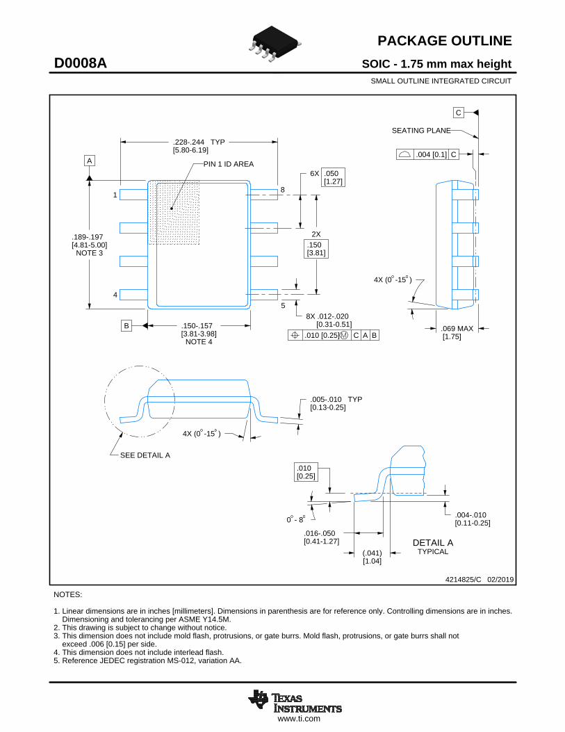
PACKAGE OUTLINE
C
.228-.244 TYP[5.80-6.19]
.069 MAX[1.75]
6X .050[1.27]
8X .012-.020 [0.31-0.51]
2X.150[3.81]
.005-.010 TYP[0.13-0.25]
0 - 8 .004-.010[0.11-0.25]
.010[0.25]
.016-.050[0.41-1.27]
4X (0 -15 )
A
.189-.197[4.81-5.00]
NOTE 3
B .150-.157[3.81-3.98]
NOTE 4
4X (0 -15 )
(.041)[1.04]
SOIC - 1.75 mm max heightD0008ASMALL OUTLINE INTEGRATED CIRCUIT
4214825/C 02/2019
NOTES: 1. Linear dimensions are in inches [millimeters]. Dimensions in parenthesis are for reference only. Controlling dimensions are in inches. Dimensioning and tolerancing per ASME Y14.5M. 2. This drawing is subject to change without notice. 3. This dimension does not include mold flash, protrusions, or gate burrs. Mold flash, protrusions, or gate burrs shall not exceed .006 [0.15] per side. 4. This dimension does not include interlead flash.5. Reference JEDEC registration MS-012, variation AA.
18
.010 [0.25] C A B
54
PIN 1 ID AREA
SEATING PLANE
.004 [0.1] C
SEE DETAIL A
DETAIL ATYPICAL
SCALE 2.800
www.ti.com
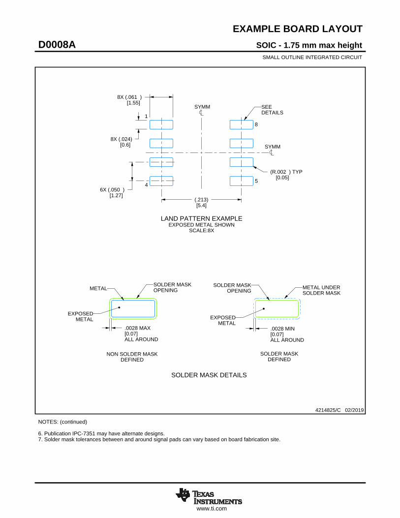
EXAMPLE BOARD LAYOUT
.0028 MAX[0.07]ALL AROUND
.0028 MIN[0.07]ALL AROUND
(.213)[5.4]
6X (.050 )[1.27]
8X (.061 )[1.55]
8X (.024)[0.6]
(R.002 ) TYP[0.05]
SOIC - 1.75 mm max heightD0008ASMALL OUTLINE INTEGRATED CIRCUIT
4214825/C 02/2019
NOTES: (continued) 6. Publication IPC-7351 may have alternate designs. 7. Solder mask tolerances between and around signal pads can vary based on board fabrication site.
METALSOLDER MASKOPENING
NON SOLDER MASKDEFINED
SOLDER MASK DETAILS
EXPOSEDMETAL
OPENINGSOLDER MASK METAL UNDER
SOLDER MASK
SOLDER MASKDEFINED
EXPOSEDMETAL
LAND PATTERN EXAMPLEEXPOSED METAL SHOWN
SCALE:8X
SYMM
1
45
8
SEEDETAILS
SYMM
www.ti.com
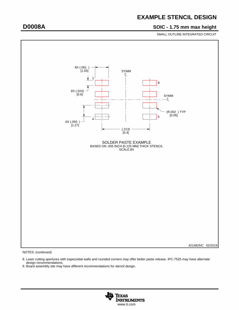
EXAMPLE STENCIL DESIGN
8X (.061 )[1.55]
8X (.024)[0.6]
6X (.050 )[1.27]
(.213)[5.4]
(R.002 ) TYP[0.05]
SOIC - 1.75 mm max heightD0008ASMALL OUTLINE INTEGRATED CIRCUIT
4214825/C 02/2019
NOTES: (continued) 8. Laser cutting apertures with trapezoidal walls and rounded corners may offer better paste release. IPC-7525 may have alternate design recommendations. 9. Board assembly site may have different recommendations for stencil design.
SOLDER PASTE EXAMPLEBASED ON .005 INCH [0.125 MM] THICK STENCIL
SCALE:8X
SYMM
SYMM
1
45
8
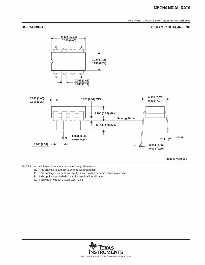
MECHANICAL DATA
MCER001A – JANUARY 1995 – REVISED JANUARY 1997
POST OFFICE BOX 655303 • DALLAS, TEXAS 75265
JG (R-GDIP-T8) CERAMIC DUAL-IN-LINE
0.310 (7,87)0.290 (7,37)
0.014 (0,36)0.008 (0,20)
Seating Plane
4040107/C 08/96
5
40.065 (1,65)0.045 (1,14)
8
1
0.020 (0,51) MIN
0.400 (10,16)0.355 (9,00)
0.015 (0,38)0.023 (0,58)
0.063 (1,60)0.015 (0,38)
0.200 (5,08) MAX
0.130 (3,30) MIN
0.245 (6,22)0.280 (7,11)
0.100 (2,54)
0°–15°
NOTES: A. All linear dimensions are in inches (millimeters).B. This drawing is subject to change without notice.C. This package can be hermetically sealed with a ceramic lid using glass frit.D. Index point is provided on cap for terminal identification.E. Falls within MIL STD 1835 GDIP1-T8


IMPORTANT NOTICE AND DISCLAIMERTI PROVIDES TECHNICAL AND RELIABILITY DATA (INCLUDING DATASHEETS), DESIGN RESOURCES (INCLUDING REFERENCEDESIGNS), APPLICATION OR OTHER DESIGN ADVICE, WEB TOOLS, SAFETY INFORMATION, AND OTHER RESOURCES “AS IS”AND WITH ALL FAULTS, AND DISCLAIMS ALL WARRANTIES, EXPRESS AND IMPLIED, INCLUDING WITHOUT LIMITATION ANYIMPLIED WARRANTIES OF MERCHANTABILITY, FITNESS FOR A PARTICULAR PURPOSE OR NON-INFRINGEMENT OF THIRDPARTY INTELLECTUAL PROPERTY RIGHTS.These resources are intended for skilled developers designing with TI products. You are solely responsible for (1) selecting the appropriateTI products for your application, (2) designing, validating and testing your application, and (3) ensuring your application meets applicablestandards, and any other safety, security, or other requirements. These resources are subject to change without notice. TI grants youpermission to use these resources only for development of an application that uses the TI products described in the resource. Otherreproduction and display of these resources is prohibited. No license is granted to any other TI intellectual property right or to any third partyintellectual property right. TI disclaims responsibility for, and you will fully indemnify TI and its representatives against, any claims, damages,costs, losses, and liabilities arising out of your use of these resources.TI’s products are provided subject to TI’s Terms of Sale (https:www.ti.com/legal/termsofsale.html) or other applicable terms available eitheron ti.com or provided in conjunction with such TI products. TI’s provision of these resources does not expand or otherwise alter TI’sapplicable warranties or warranty disclaimers for TI products.IMPORTANT NOTICE
Mailing Address: Texas Instruments, Post Office Box 655303, Dallas, Texas 75265Copyright © 2021, Texas Instruments Incorporated
Recommended