Timers
Chapter 10
Timers
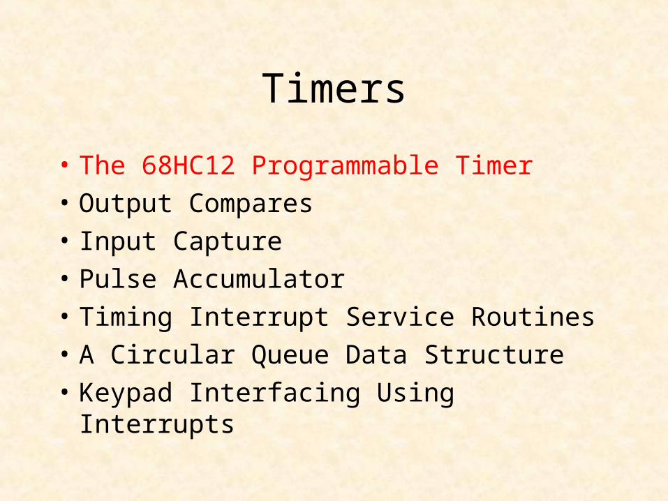
• The 68HC12 Programmable Timer
• Output Compares
• Input Capture
• Pulse Accumulator
• Timing Interrupt Service Routines
• A Circular Queue Data Structure
• Keypad Interfacing Using Interrupts

Timers (cont.)
• Pulse Train Using Interrupts
• Measuring the Period of a Pulse Train Using Interrupts
• The Polaroid Ultrasonic Transducer– An Ultrasonic Tape Measure
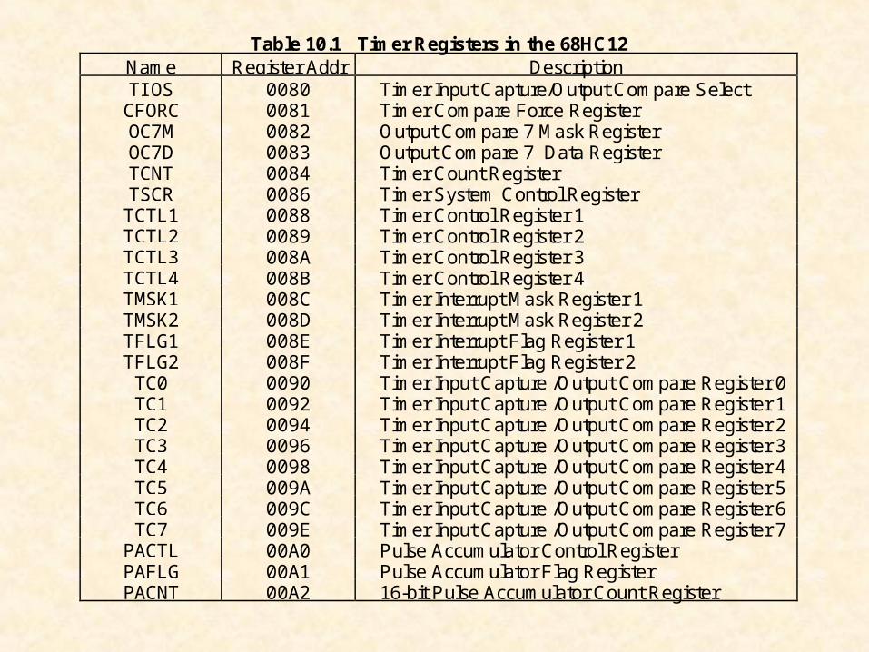
Table 10.1 Timer Registers in the 68HC12Name Register Addr DescriptionTIOS 0080 Timer Input Capture/Output Compare SelectCFORC 0081 Timer Compare Force RegisterOC7M 0082 Output Compare 7 Mask RegisterOC7D 0083 Output Compare 7 Data RegisterTCNT 0084 Timer Count RegisterTSCR 0086 Timer System Control RegisterTCTL1 0088 Timer Control Register 1TCTL2 0089 Timer Control Register 2TCTL3 008A Timer Control Register 3TCTL4 008B Timer Control Register 4TMSK1 008C Timer Interrupt Mask Register 1TMSK2 008D Timer Interrupt Mask Register 2TFLG1 008E Timer Interrupt Flag Register 1TFLG2 008F Timer Interrupt Flag Register 2TC0 0090 Timer Input Capture /Output Compare Register 0TC1 0092 Timer Input Capture /Output Compare Register 1TC2 0094 Timer Input Capture /Output Compare Register 2TC3 0096 Timer Input Capture /Output Compare Register 3TC4 0098 Timer Input Capture /Output Compare Register 4TC5 009A Timer Input Capture /Output Compare Register 5TC6 009C Timer Input Capture /Output Compare Register 6TC7 009E Timer Input Capture /Output Compare Register 7PACTL 00A0 Pulse Accumulator Control RegisterPAFLG 00A1 Pulse Accumulator Flag RegisterPACNT 00A2 16-bit Pulse Accumulator Count Register
Timer Counter
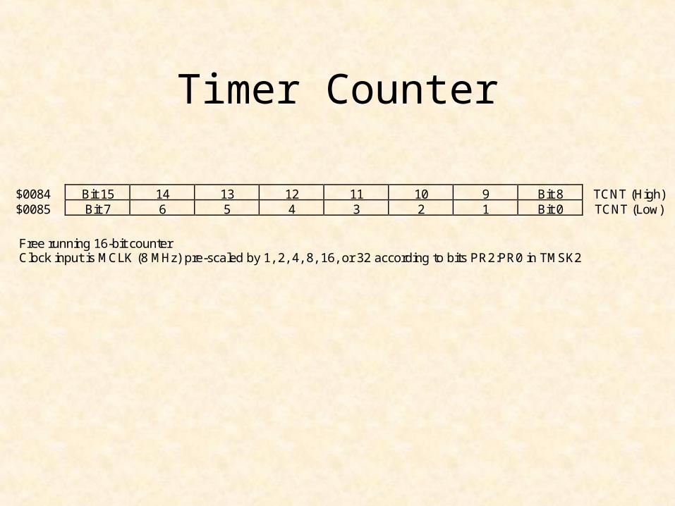
$0084 Bit 15 14 13 12 11 10 9 Bit 8 TCNT (High)$0085 Bit 7 6 5 4 3 2 1 Bit 0 TCNT (Low)
Free running 16-bit counterClock input is MCLK (8 MHz) pre-scaled by 1, 2, 4, 8, 16, or 32 according to bits PR2:PR0 in TMSK2
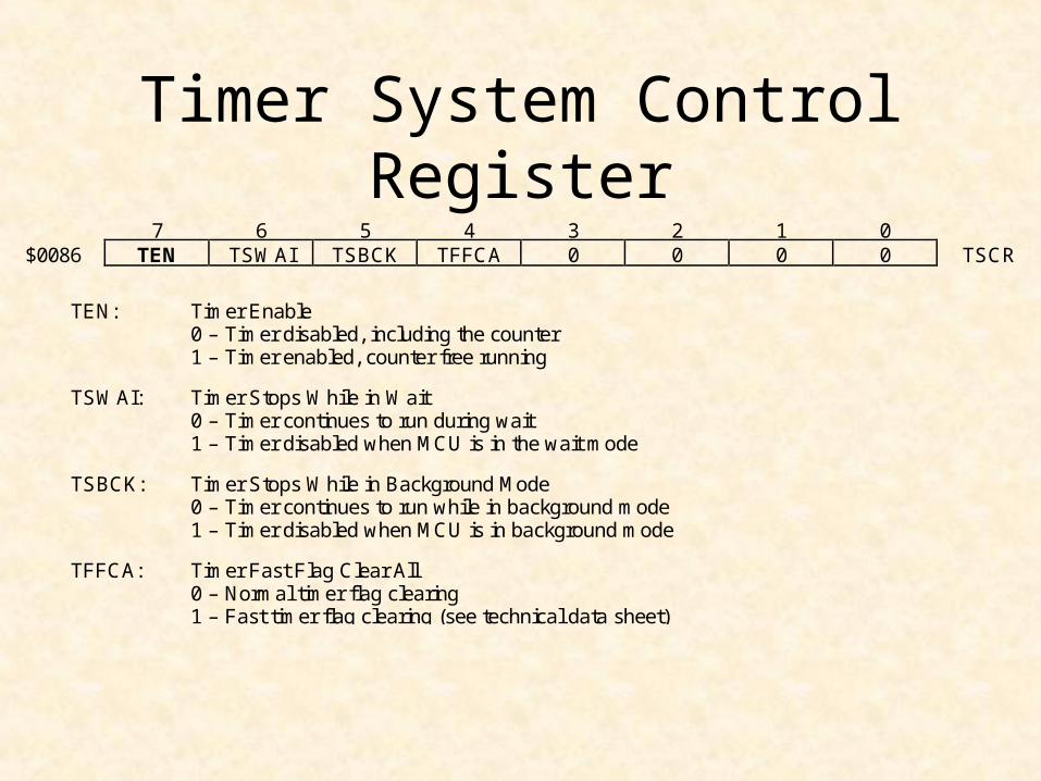
Timer System Control Register7 6 5 4 3 2 1 0
$0086 TEN TSWAI TSBCK TFFCA 0 0 0 0 TSCR
TEN: Timer Enable0 – Timer disabled, including the counter1 – Timer enabled, counter free running
TSWAI: Timer Stops While in Wait0 – Timer continues to run during wait1 – Timer disabled when MCU is in the wait mode
TSBCK: Timer Stops While in Background Mode0 – Timer continues to run while in background mode1 – Timer disabled when MCU is in background mode
TFFCA: Timer Fast Flag Clear All0 – Normal timer flag clearing1 – Fast timer flag clearing (see technical data sheet)
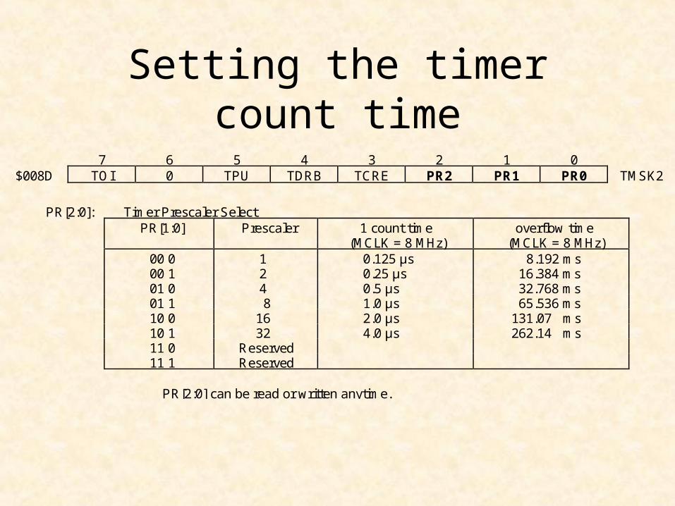
Setting the timer count time
7 6 5 4 3 2 1 0$008D TOI 0 TPU TDRB TCRE PR2 PR1 PR0 TMSK2
PR[2:0]: Timer Prescaler SelectPR[1:0] Prescaler 1 count time
(MCLK = 8 MHz)overflow time
(MCLK = 8 MHz)00 0 1 0.125 µs 8.192 ms00 1 2 0.25 µs 16.384 ms01 0 4 0.5 µs 32.768 ms01 1 8 1.0 µs 65.536 ms10 0 16 2.0 µs 131.07 ms10 1 32 4.0 µs 262.14 ms11 0 Reserved11 1 Reserved
PR[2:0] can be read or written anytime.
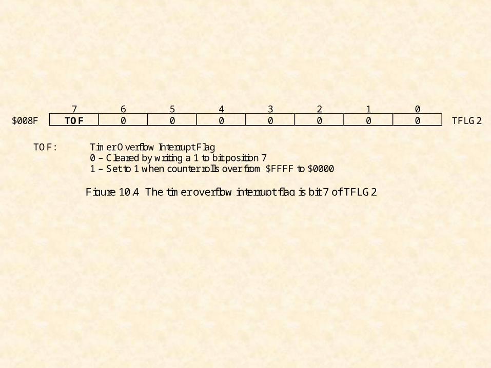
7 6 5 4 3 2 1 0$008F TOF 0 0 0 0 0 0 0 TFLG2
TOF: Timer Overflow Interrupt Flag0 – Cleared by writing a 1 to bit position 71 – Set to 1 when counter rolls over from $FFFF to $0000
Figure 10.4 The timer overflow interrupt flag is bit 7 of TFLG2
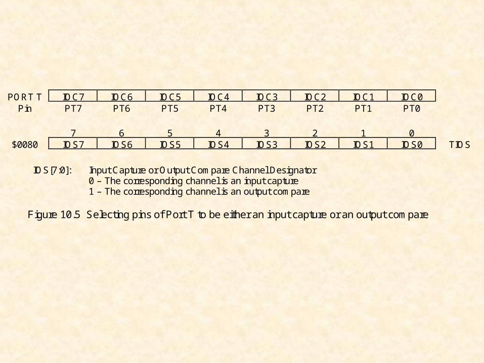
PORT T IOC7 IOC6 IOC5 IOC4 IOC3 IOC2 IOC1 IOC0Pin PT7 PT6 PT5 PT4 PT3 PT2 PT1 PT0
7 6 5 4 3 2 1 0$0080 IOS7 IOS6 IOS5 IOS4 IOS3 IOS2 IOS1 IOS0 TIOS
IOS[7:0]: Input Capture or Output Compare Channel Designator0 – The corresponding channel is an input capture1 – The corresponding channel is an output compare
Figure 10.5 Selecting pins of Port T to be either an input capture or an output compare

68HC11 Timer RegistersTable 10.2 Timer Registers in the 68HC11
Name Register Addr DescriptionCFORC 100B Compare Force RegisterOC1M 100C OC1 Action Mask RegisterOC1D 100D OC1 Action Data RegisterTCNT 100E Timer Counter RegisterTIC1 1010 Input Capture 1 RegisterTIC2 1012 Input Capture 2 RegisterTIC3 1014 Input Capture 3 RegisterTOC1 1016 Output Compare 1 RegisterTOC2 1018 Output Compare 2 RegisterTOC3 101A Output Compare 3 RegisterTOC4 101C Output Compare 4 RegisterTI4O5 101E Input Capture 4/Output Compare 5 RegTCTL1 1020 Timer Control Register 1TCTL2 1021 Timer Control Register 2TMSK1 1022 Timer Interrupt Mask Register 1TFLG1 1023 Timer Interrupt Flag Register 1TMSK2 1024 Timer Interrupt Mask Register 2TFLG2 1025 Timer Interrupt Flag Register 2PACTL 1026 Pulse Accumulator Control RegisterPACNT 1027 Pulse Accumulator Count Register
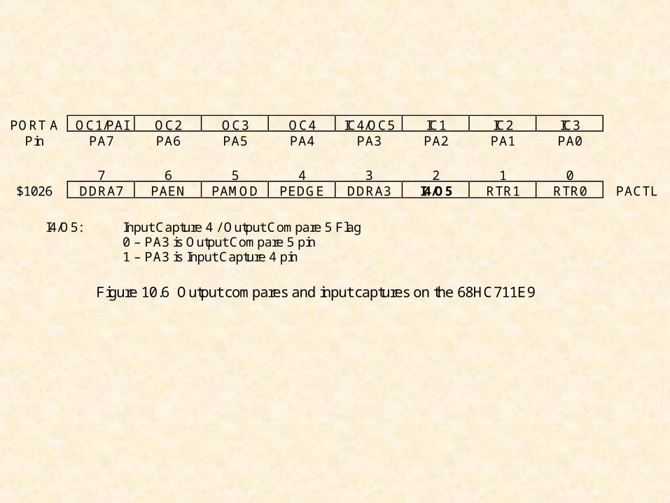
PORT A OC1/PAI OC2 OC3 OC4 IC4/OC5 IC1 IC2 IC3Pin PA7 PA6 PA5 PA4 PA3 PA2 PA1 PA0
7 6 5 4 3 2 1 0$1026 DDRA7 PAEN PAMOD PEDGE DDRA3 I4/O5 RTR1 RTR0 PACTL
I4/O5: Input Capture 4 / Output Compare 5 Flag0 – PA3 is Output Compare 5 pin1 – PA3 is Input Capture 4 pin
Figure 10.6 Output compares and input captures on the 68HC711E9
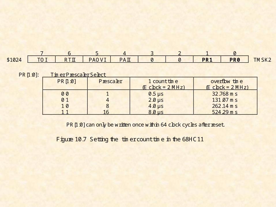
7 6 5 4 3 2 1 0$1024 TOI RTII PAOVI PAII 0 0 PR1 PR0 TMSK2
PR[1:0]: Timer Prescaler SelectPR[1:0] Prescaler 1 count time
(E clock = 2 MHz)overflow time
(E clock = 2 MHz)0 0 1 0.5 µs 32.768 ms0 1 4 2.0 µs 131.07 ms1 0 8 4.0 µs 262.14 ms1 1 16 8.0 µs 524.29 ms
PR[1:0] can only be written once within 64 clock cycles after reset.
Figure 10.7 Setting the timer count time in the 68HC11
Timers
• The 68HC12 Programmable Timer
• Output Compares
• Input Capture
• Pulse Accumulator
• Timing Interrupt Service Routines
• A Circular Queue Data Structure
• Keypad Interfacing Using Interrupts
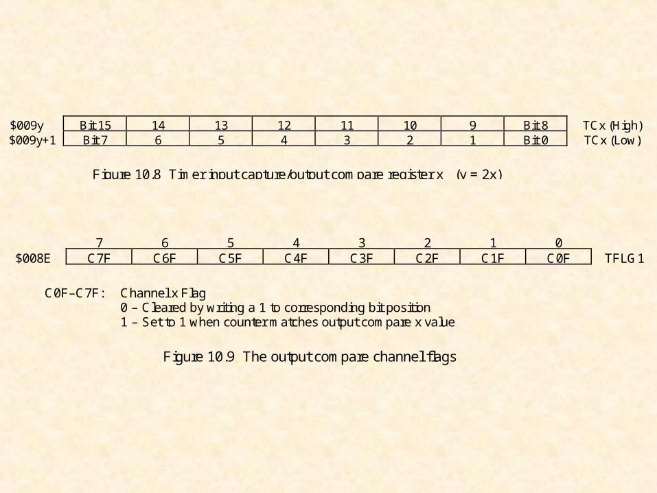
$009y Bit 15 14 13 12 11 10 9 Bit 8 TCx (High)$009y+1 Bit 7 6 5 4 3 2 1 Bit 0 TCx (Low)
Figure 10.8 Timer input capture/output compare register x (y = 2x)
7 6 5 4 3 2 1 0$008E C7F C6F C5F C4F C3F C2F C1F C0F TFLG1
C0F–C7F: Channel x Flag0 – Cleared by writing a 1 to corresponding bit position1 – Set to 1 when counter matches output compare x value
Figure 10.9 The output compare channel flags
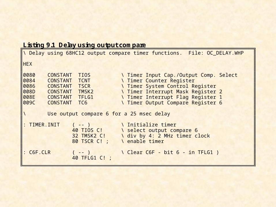
Listing 9.1 Delay using output compare\ Delay using 68HC12 output compare timer functions. File: OC_DELAY.WHP
HEX
0080 CONSTANT TIOS \ Timer Input Cap./Output Comp. Select0084 CONSTANT TCNT \ Timer Counter Register0086 CONSTANT TSCR \ Timer System Control Register008D CONSTANT TMSK2 \ Timer Interrupt Mask Register 2008E CONSTANT TFLG1 \ Timer Interrupt Flag Register 1009C CONSTANT TC6 \ Timer Output Compare Register 6
\ Use output compare 6 for a 25 msec delay
: TIMER.INIT ( -- ) \ Initialize timer 40 TIOS C! \ select output compare 6 32 TMSK2 C! \ div by 4: 2 MHz timer clock 80 TSCR C! ; \ enable timer
: C6F.CLR ( -- ) \ Clear C6F - bit 6 - in TFLG1 ) 40 TFLG1 C! ;
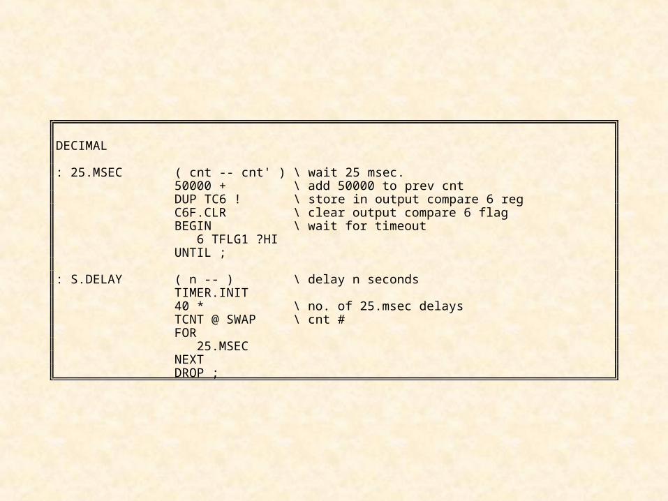
DECIMAL
: 25.MSEC ( cnt -- cnt' ) \ wait 25 msec. 50000 + \ add 50000 to prev cnt DUP TC6 ! \ store in output compare 6 reg C6F.CLR \ clear output compare 6 flag BEGIN \ wait for timeout 6 TFLG1 ?HI UNTIL ;
: S.DELAY ( n -- ) \ delay n seconds TIMER.INIT 40 * \ no. of 25.msec delays TCNT @ SWAP \ cnt # FOR 25.MSEC NEXT DROP ;
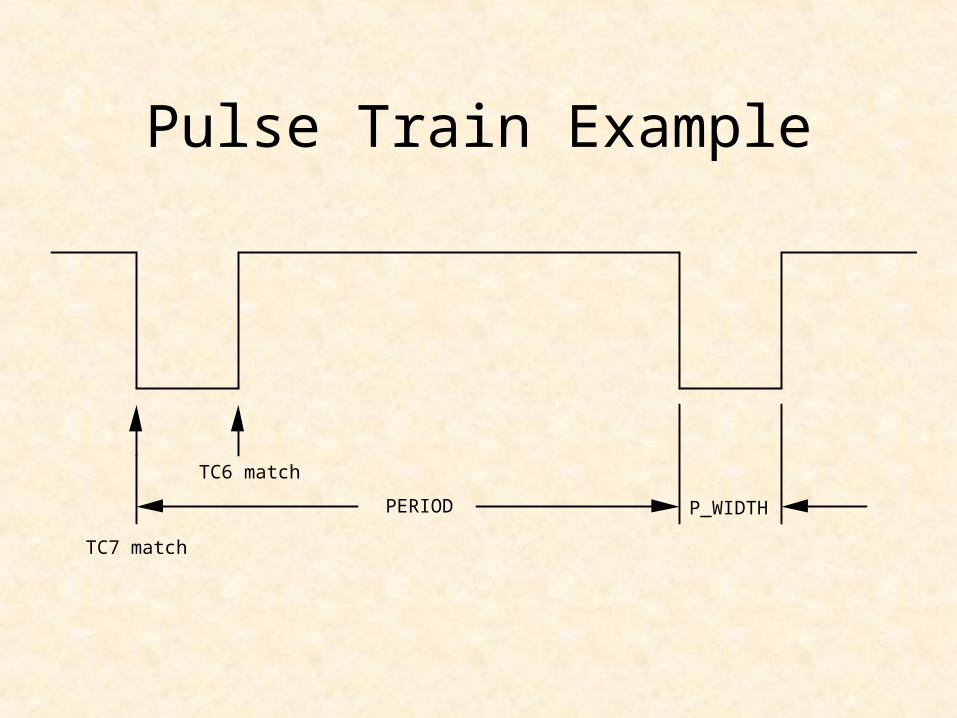
Pulse Train Example
TC6 match
TC7 match
PERIOD P_WIDTH
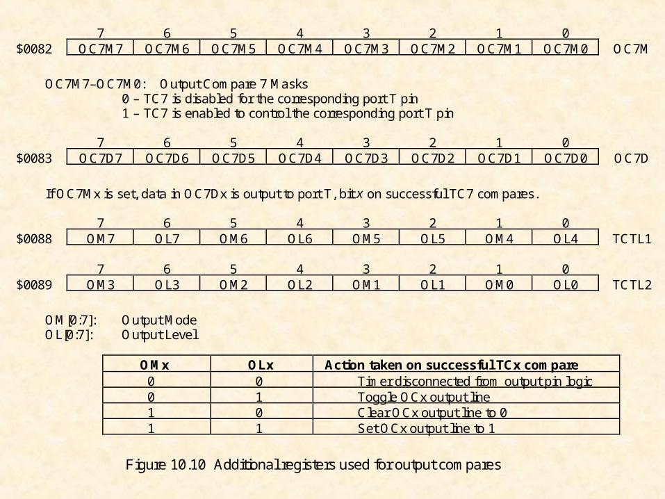
7 6 5 4 3 2 1 0$0082 OC7M7 OC7M6 OC7M5 OC7M4 OC7M3 OC7M2 OC7M1 OC7M0 OC7M
OC7M7–OC7M0: Output Compare 7 Masks0 – TC7 is disabled for the corresponding port T pin1 – TC7 is enabled to control the corresponding port T pin
7 6 5 4 3 2 1 0$0083 OC7D7 OC7D6 OC7D5 OC7D4 OC7D3 OC7D2 OC7D1 OC7D0 OC7D
If OC7Mx is set, data in OC7Dx is output to port T, bit x on successful TC7 compares.
7 6 5 4 3 2 1 0$0088 OM7 OL7 OM6 OL6 OM5 OL5 OM4 OL4 TCTL1
7 6 5 4 3 2 1 0$0089 OM3 OL3 OM2 OL2 OM1 OL1 OM0 OL0 TCTL2
OM[0:7]: Output ModeOL[0:7]: Output Level
OMx OLx Action taken on successful TCx compare0 0 Timer disconnected from output pin logic0 1 Toggle OCx output line1 0 Clear OCx output line to 01 1 Set OCx output line to 1
Figure 10.10 Additional registers used for output compares
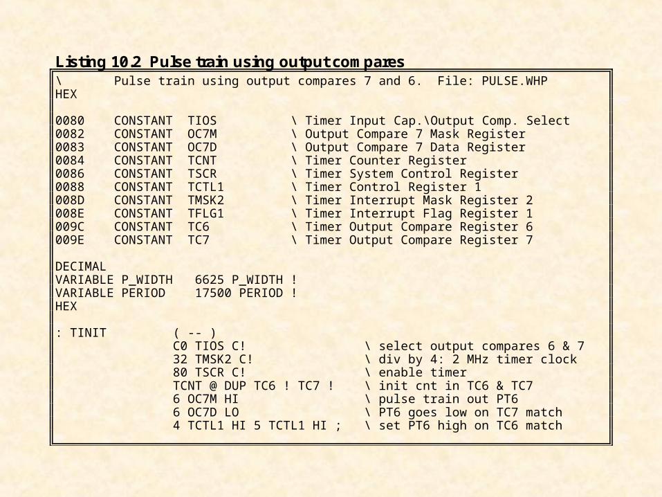
Listing 10.2 Pulse train using output compares\ Pulse train using output compares 7 and 6. File: PULSE.WHPHEX
0080 CONSTANT TIOS \ Timer Input Cap.\Output Comp. Select0082 CONSTANT OC7M \ Output Compare 7 Mask Register0083 CONSTANT OC7D \ Output Compare 7 Data Register0084 CONSTANT TCNT \ Timer Counter Register0086 CONSTANT TSCR \ Timer System Control Register0088 CONSTANT TCTL1 \ Timer Control Register 1008D CONSTANT TMSK2 \ Timer Interrupt Mask Register 2008E CONSTANT TFLG1 \ Timer Interrupt Flag Register 1009C CONSTANT TC6 \ Timer Output Compare Register 6009E CONSTANT TC7 \ Timer Output Compare Register 7
DECIMALVARIABLE P_WIDTH 6625 P_WIDTH !VARIABLE PERIOD 17500 PERIOD !HEX
: TINIT ( -- ) C0 TIOS C! \ select output compares 6 & 7 32 TMSK2 C! \ div by 4: 2 MHz timer clock 80 TSCR C! \ enable timer TCNT @ DUP TC6 ! TC7 ! \ init cnt in TC6 & TC7 6 OC7M HI \ pulse train out PT6 6 OC7D LO \ PT6 goes low on TC7 match 4 TCTL1 HI 5 TCTL1 HI ; \ set PT6 high on TC6 match
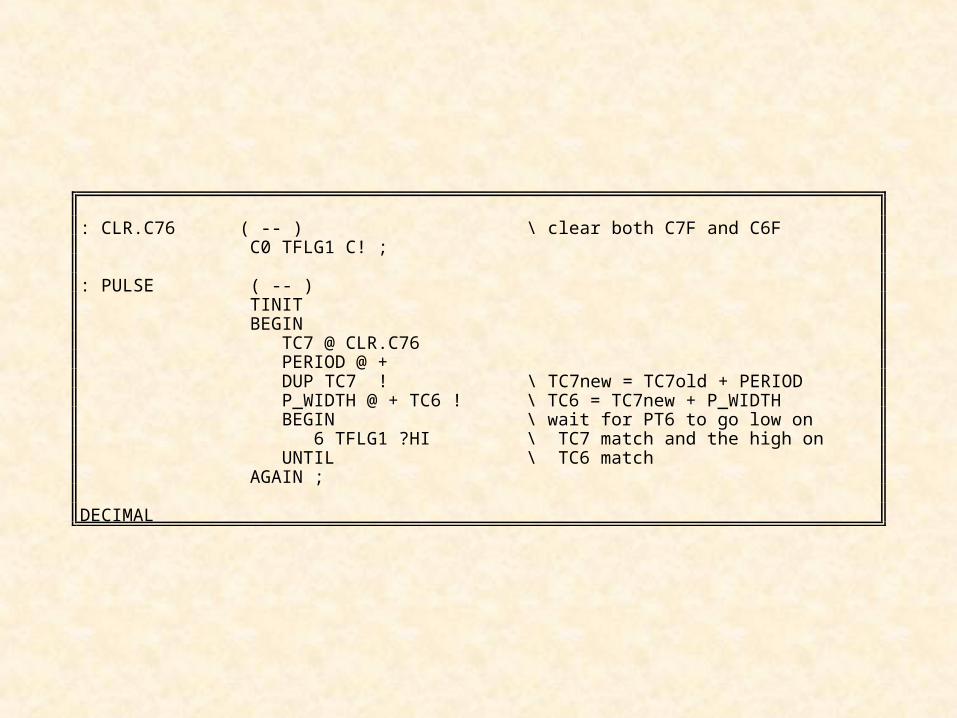
: CLR.C76 ( -- ) \ clear both C7F and C6F C0 TFLG1 C! ;
: PULSE ( -- ) TINIT BEGIN TC7 @ CLR.C76 PERIOD @ + DUP TC7 ! \ TC7new = TC7old + PERIOD P_WIDTH @ + TC6 ! \ TC6 = TC7new + P_WIDTH BEGIN \ wait for PT6 to go low on 6 TFLG1 ?HI \ TC7 match and the high on UNTIL \ TC6 match AGAIN ;
DECIMAL
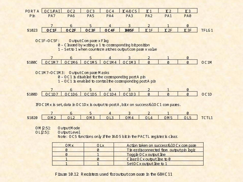
PORT A OC1/PAI OC2 OC3 OC4 IC4/OC5 IC1 IC2 IC3Pin PA7 PA6 PA5 PA4 PA3 PA2 PA1 PA0
7 6 5 4 3 2 1 0$1023 OC1F OC2F OC3F OC4F I405F IC1F IC2F IC3F TFLG1
OC1F–OC5F: Output Compare x Flag0 – Cleared by writing a 1 to corresponding bit position1 – Set to 1 when counter matches output compare x value
7 6 5 4 3 2 1 0$100C OC1M7 OC1M6 OC1M5 OC1M4 OC1M3 0 0 0 OC1M
OC1M7–OC1M3: Output Compare Masks0 – OC1 is disabled for the corresponding port A pin1 – OC1 is enabled to control the corresponding port A pin
7 6 5 4 3 2 1 0$100D OC1D7 OC1D6 OC1D5 OC1D4 OC1D3 0 0 0 OC1D
If OC1Mx is set, data in OC1Dx is output to port A, bit x on successful OC1 compares.
7 6 5 4 3 2 1 0$1020 OM2 OL2 OM3 OL3 OM4 OL4 OM5 OL5 TCTL1
OM[2:5]: Output ModeOL[2:5]: Output Level
Note: OC5 functions only if the I4/O5 bit in the PACTL register is clear.
OMx OLx Action taken on successful OCx compare0 0 Timer disconnected from output pin logic0 1 Toggle OCx output line1 0 Clear OCx output line to 01 1 Set OCx output line to 1
Figure 10.12 Registers used for output compare in the 68HC11
Timers
• The 68HC12 Programmable Timer
• Output Compares
• Input Capture
• Pulse Accumulator
• Timing Interrupt Service Routines
• A Circular Queue Data Structure
• Keypad Interfacing Using Interrupts
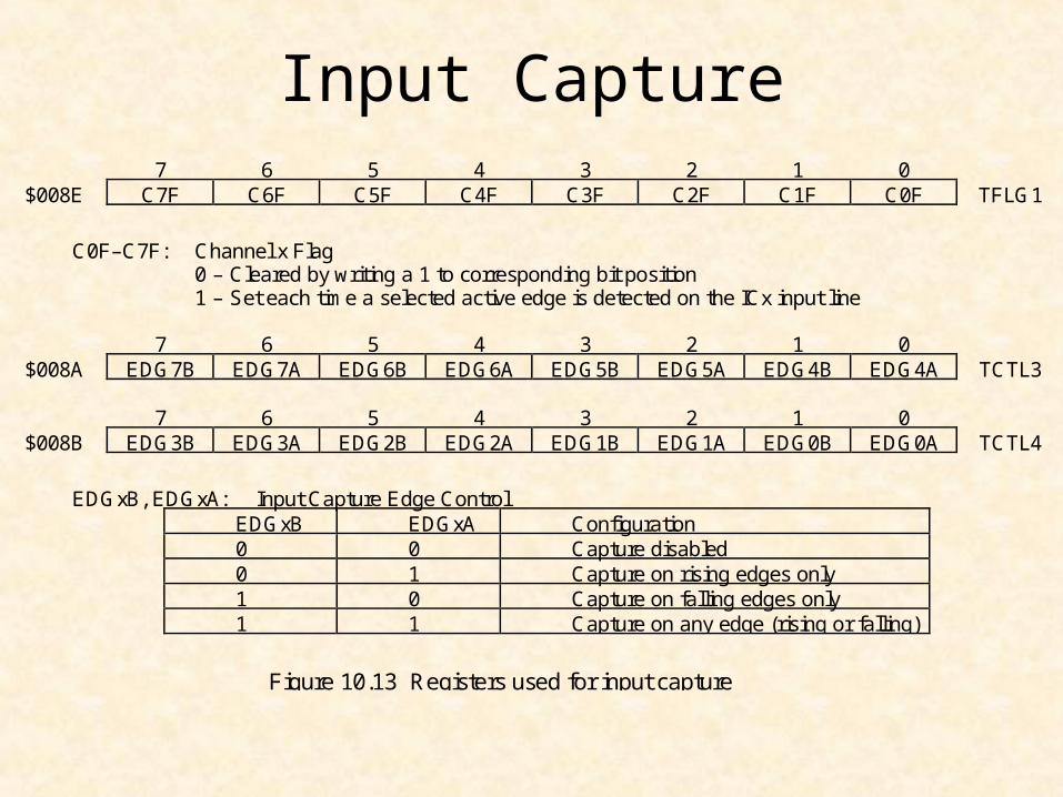
Input Capture7 6 5 4 3 2 1 0
$008E C7F C6F C5F C4F C3F C2F C1F C0F TFLG1
C0F–C7F: Channel x Flag0 – Cleared by writing a 1 to corresponding bit position1 – Set each time a selected active edge is detected on the ICx input line
7 6 5 4 3 2 1 0$008A EDG7B EDG7A EDG6B EDG6A EDG5B EDG5A EDG4B EDG4A TCTL3
7 6 5 4 3 2 1 0$008B EDG3B EDG3A EDG2B EDG2A EDG1B EDG1A EDG0B EDG0A TCTL4
EDGxB, EDGxA: Input Capture Edge ControlEDGxB EDGxA Configuration0 0 Capture disabled0 1 Capture on rising edges only1 0 Capture on falling edges only1 1 Capture on any edge (rising or falling)
Figure 10.13 Registers used for input capture
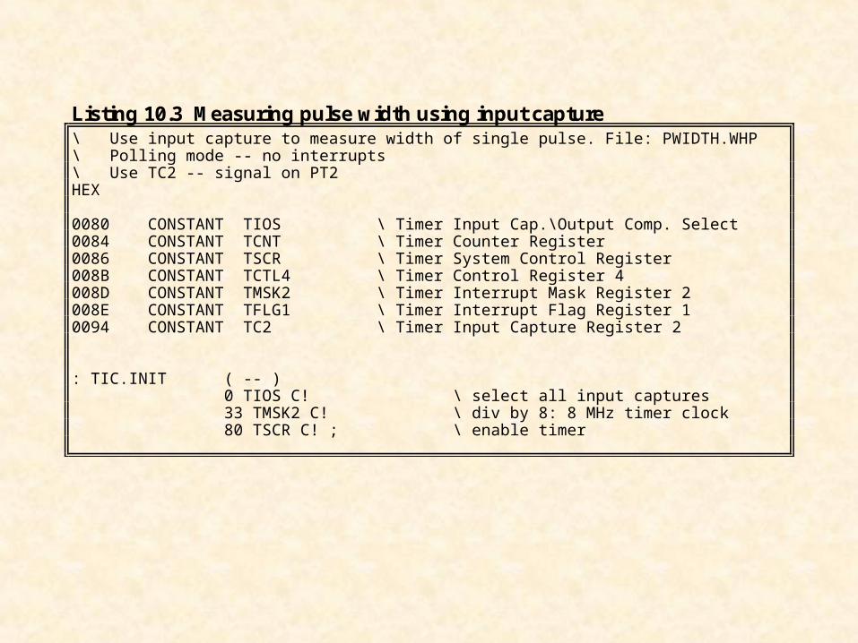
Listing 10.3 Measuring pulse width using input capture\ Use input capture to measure width of single pulse. File: PWIDTH.WHP\ Polling mode -- no interrupts\ Use TC2 -- signal on PT2HEX
0080 CONSTANT TIOS \ Timer Input Cap.\Output Comp. Select0084 CONSTANT TCNT \ Timer Counter Register0086 CONSTANT TSCR \ Timer System Control Register008B CONSTANT TCTL4 \ Timer Control Register 4008D CONSTANT TMSK2 \ Timer Interrupt Mask Register 2008E CONSTANT TFLG1 \ Timer Interrupt Flag Register 10094 CONSTANT TC2 \ Timer Input Capture Register 2
: TIC.INIT ( -- ) 0 TIOS C! \ select all input captures 33 TMSK2 C! \ div by 8: 8 MHz timer clock 80 TSCR C! ; \ enable timer
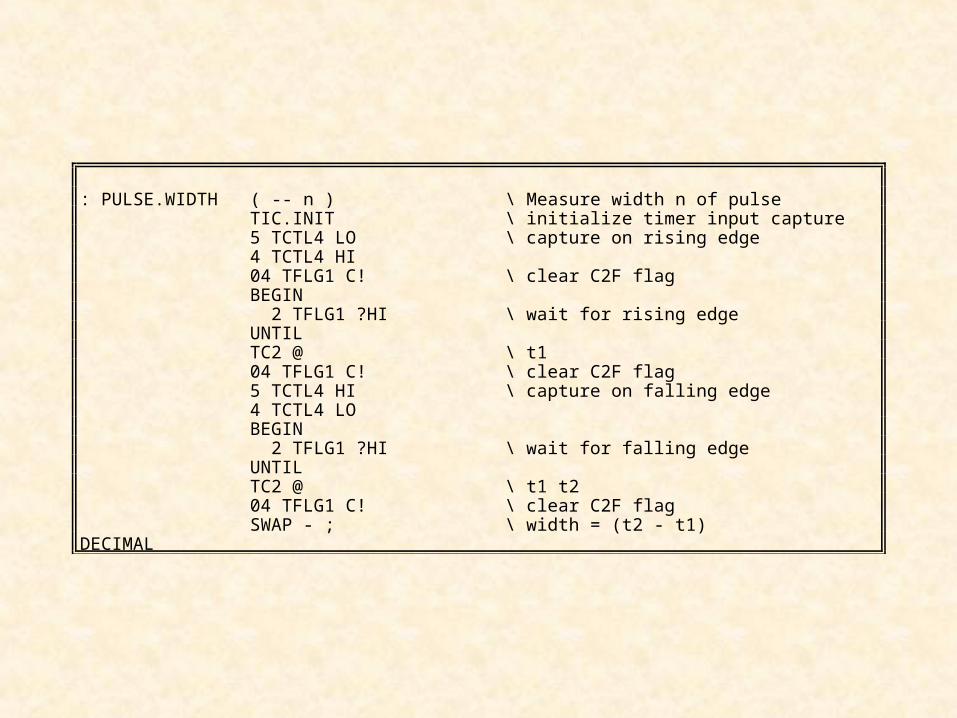
: PULSE.WIDTH ( -- n ) \ Measure width n of pulse TIC.INIT \ initialize timer input capture 5 TCTL4 LO \ capture on rising edge 4 TCTL4 HI 04 TFLG1 C! \ clear C2F flag BEGIN 2 TFLG1 ?HI \ wait for rising edge UNTIL TC2 @ \ t1 04 TFLG1 C! \ clear C2F flag 5 TCTL4 HI \ capture on falling edge 4 TCTL4 LO BEGIN 2 TFLG1 ?HI \ wait for falling edge UNTIL TC2 @ \ t1 t2 04 TFLG1 C! \ clear C2F flag SWAP - ; \ width = (t2 - t1)DECIMAL
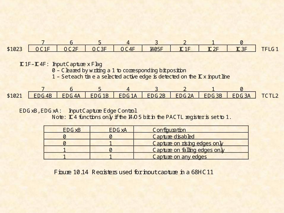
7 6 5 4 3 2 1 0$1023 OC1F OC2F OC3F OC4F I405F IC1F IC2F IC3F TFLG1
IC1F–IC4F: Input Capture x Flag0 – Cleared by writing a 1 to corresponding bit position1 – Set each time a selected active edge is detected on the ICx input line
7 6 5 4 3 2 1 0$1021 EDG4B EDG4A EDG1B EDG1A EDG2B EDG2A EDG3B EDG3A TCTL2
EDGxB, EDGxA: Input Capture Edge ControlNote: IC4 functions only if the I4/O5 bit in the PACTL register is set to 1.
EDGxB EDGxA Configuration0 0 Capture disabled0 1 Capture on rising edges only1 0 Capture on falling edges only1 1 Capture on any edges
Figure 10.14 Registers used for input capture in a 68HC11
Timers
• The 68HC12 Programmable Timer
• Output Compares
• Input Capture
• Pulse Accumulator
• Timing Interrupt Service Routines
• A Circular Queue Data Structure
• Keypad Interfacing Using Interrupts
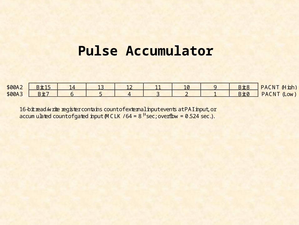
$00A2 Bit 15 14 13 12 11 10 9 Bit 8 PACNT (High)$00A3 Bit 7 6 5 4 3 2 1 Bit 0 PACNT (Low)
16-bit read/write register contains count of external input events at PAI input, oraccumulated count of gated input (MCLK / 64 = 8 sec; overflow = 0.524 sec.).
Pulse Accumulator
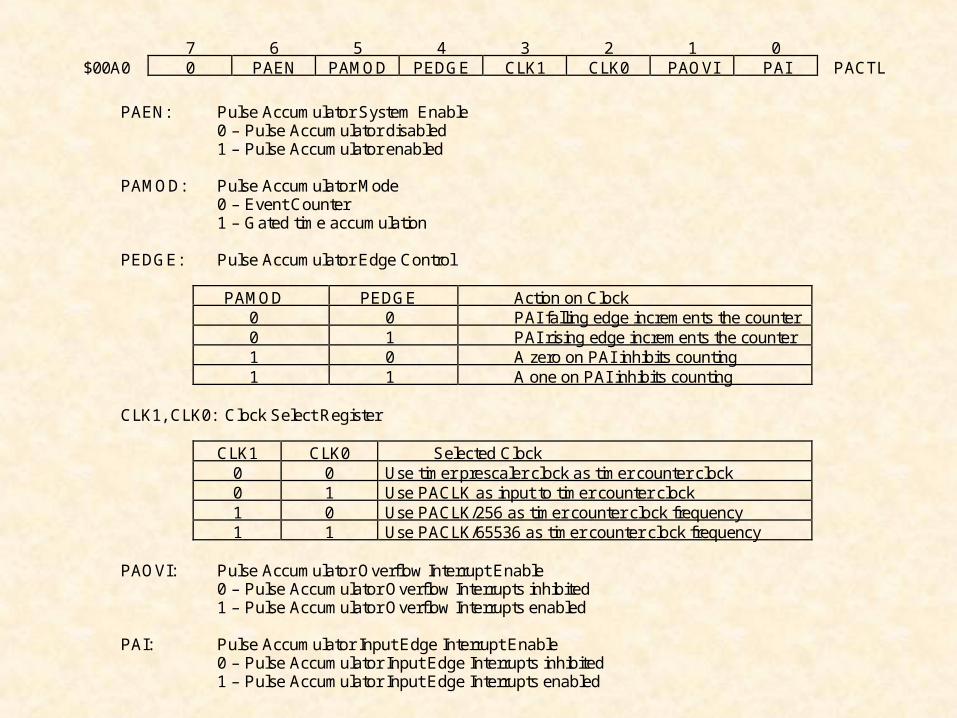
7 6 5 4 3 2 1 0$00A0 0 PAEN PAMOD PEDGE CLK1 CLK0 PAOVI PAI PACTL
PAEN: Pulse Accumulator System Enable0 – Pulse Accumulator disabled1 – Pulse Accumulator enabled
PAMOD: Pulse Accumulator Mode0 – Event Counter1 – Gated time accumulation
PEDGE: Pulse Accumulator Edge Control
PAMOD PEDGE Action on Clock0 0 PAI falling edge increments the counter0 1 PAI rising edge increments the counter1 0 A zero on PAI inhibits counting1 1 A one on PAI inhibits counting
CLK1, CLK0: Clock Select Register
CLK1 CLK0 Selected Clock0 0 Use timer prescaler clock as timer counter clock0 1 Use PACLK as input to timer counter clock1 0 Use PACLK/256 as timer counter clock frequency1 1 Use PACLK/65536 as timer counter clock frequency
PAOVI: Pulse Accumulator Overflow Interrupt Enable0 – Pulse Accumulator Overflow Interrupts inhibited1 – Pulse Accumulator Overflow Interrupts enabled
PAI: Pulse Accumulator Input Edge Interrupt Enable0 – Pulse Accumulator Input Edge Interrupts inhibited1 – Pulse Accumulator Input Edge Interrupts enabled
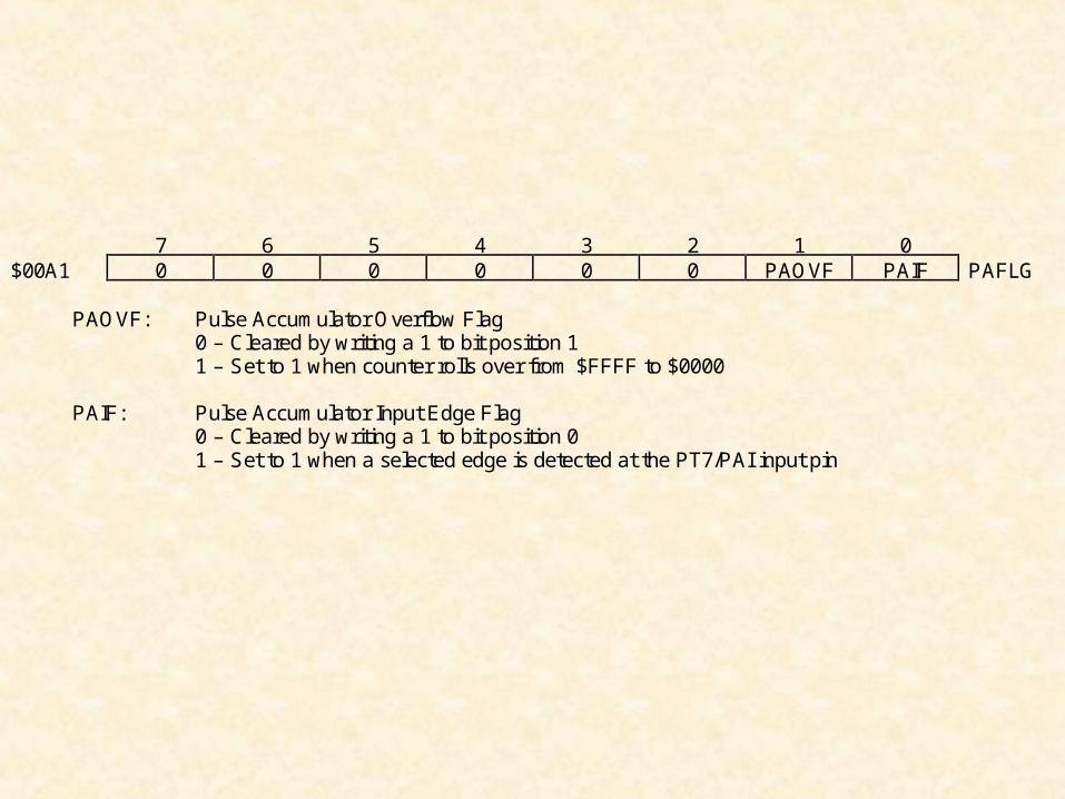
7 6 5 4 3 2 1 0$00A1 0 0 0 0 0 0 PAOVF PAIF PAFLG
PAOVF: Pulse Accumulator Overflow Flag0 – Cleared by writing a 1 to bit position 11 – Set to 1 when counter rolls over from $FFFF to $0000
PAIF: Pulse Accumulator Input Edge Flag0 – Cleared by writing a 1 to bit position 01 – Set to 1 when a selected edge is detected at the PT7/PAI input pin
1
2
3
4
5
6
7
9
8
Vcc
ROW Y3
ROW Y4
OSC
KB MASK
COL X4
COL X3
ROW Y2
ROW Y1
DATA OUT A
DATA OUT D
OUT EN
DATA AV
COL X1
COL X2
DATA OUT C
DATA OUT B
18
17
16
15
14
13
12
11
10GND
MM74C922
PJ0
PJ1
PJ2
PJ3
PJ7
0.1f
1.0f
X1 X2 X3 X4 Y4 Y3 Y2 Y1
NC
0123
4567
89B
C
A
DEF
1 2 3
4 5 6
7 8 9
0A B
C
D
E
F
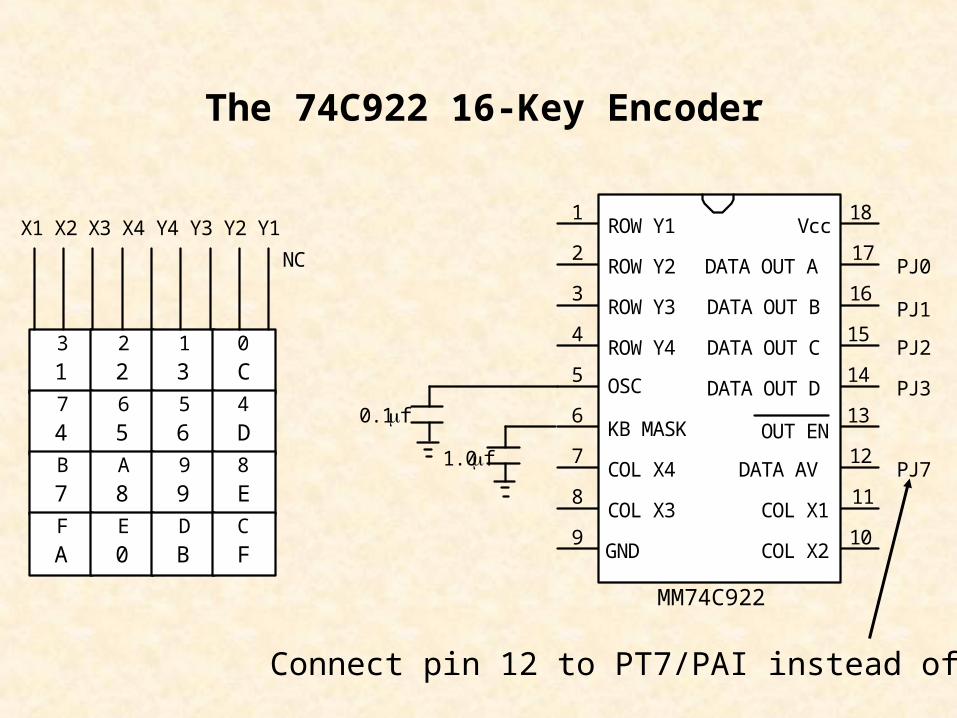
The 74C922 16-Key Encoder
Connect pin 12 to PT7/PAI instead of PJ7
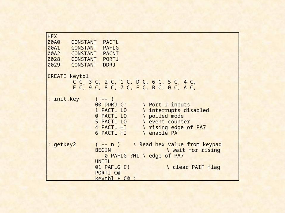
HEX00A0 CONSTANT PACTL00A1 CONSTANT PAFLG00A2 CONSTANT PACNT0028 CONSTANT PORTJ0029 CONSTANT DDRJ
CREATE keytbl C C, 3 C, 2 C, 1 C, D C, 6 C, 5 C, 4 C, E C, 9 C, 8 C, 7 C, F C, B C, 0 C, A C,
: init.key ( -- ) 00 DDRJ C! \ Port J inputs
1 PACTL LO \ interrupts disabled0 PACTL LO \ polled mode5 PACTL LO \ event counter4 PACTL HI \ rising edge of PA76 PACTL HI \ enable PA
: getkey2 ( -- n ) \ Read hex value from keypad BEGIN \ wait for rising 0 PAFLG ?HI \ edge of PA7 UNTIL
01 PAFLG C! \ clear PAIF flag PORTJ C@ keytbl + C@ ;

Pulse Accumulator on a 68HC11
7 6 5 4 3 2 1 0$1027 Bit 7 6 5 4 3 2 1 Bit 0 PACNT
8-bit read/write register contains count of external input events at PAI input, or accumulatedcount of gated input (E-clock / 64 = 32 sec; overflow = 8.192 msec.).
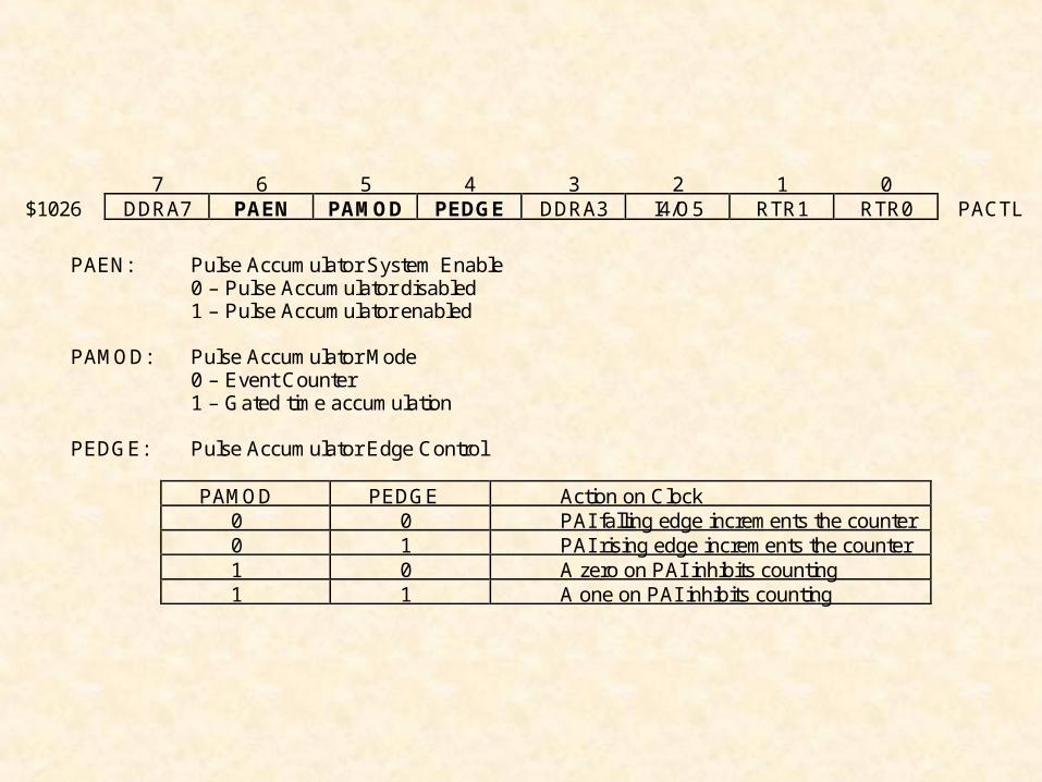
7 6 5 4 3 2 1 0$1026 DDRA7 PAEN PAMOD PEDGE DDRA3 I4/O5 RTR1 RTR0 PACTL
PAEN: Pulse Accumulator System Enable0 – Pulse Accumulator disabled1 – Pulse Accumulator enabled
PAMOD: Pulse Accumulator Mode0 – Event Counter1 – Gated time accumulation
PEDGE: Pulse Accumulator Edge Control
PAMOD PEDGE Action on Clock0 0 PAI falling edge increments the counter0 1 PAI rising edge increments the counter1 0 A zero on PAI inhibits counting1 1 A one on PAI inhibits counting

7 6 5 4 3 2 1 0$1025 TOF RTIF PAOVF PAIF 0 0 0 0 TFLG2
PAOVF: Pulse Accumulator Overflow Interrupt Flag0 – Cleared by writing a 1 to bit position 51 – Set to 1 when counter rolls over from $FF to $00
PAIF: Pulse Accumulator Input Edge Interrupt Flag0 – Cleared by writing a 1 to bit position 41 – Set to 1 when a selected edge is detected at the PA7/PAI input pin
7 6 5 4 3 2 1 0$1024 TOI RTII PAOVI PAI 0 0 PR1 PR0 TMSK2
PAOVI: Pulse Accumulator Overflow Interrupt Enable0 – Pulse Accumulator Overflow Interrupts inhibited1 – Pulse Accumulator Overflow Interrupts enabled
PAI: Pulse Accumulator Input Edge Interrupt Enable0 – Pulse Accumulator Input Edge Interrupts inhibited1 – Pulse Accumulator Input Edge Interrupts enabled

Timers
• The 68HC12 Programmable Timer
• Output Compares
• Input Capture
• Pulse Accumulator
• Timing Interrupt Service Routines
• A Circular Queue Data Structure
• Keypad Interfacing Using Interrupts
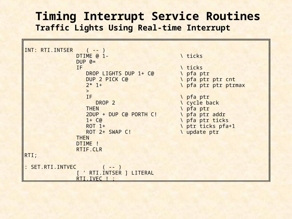
Timing Interrupt Service RoutinesTraffic Lights Using Real-time Interrupt
INT: RTI.INTSER ( -- ) DTIME @ 1- \ ticks DUP 0= IF \ ticks DROP LIGHTS DUP 1+ C@ \ pfa ptr DUP 2 PICK C@ \ pfa ptr ptr cnt 2* 1+ \ pfa ptr ptr ptrmax > IF \ pfa ptr DROP 2 \ cycle back THEN \ pfa ptr 2DUP + DUP C@ PORTH C! \ pfa ptr addr 1+ C@ \ pfa ptr ticks ROT 1+ \ ptr ticks pfa+1 ROT 2+ SWAP C! \ update ptr THEN DTIME ! RTIF.CLRRTI;
: SET.RTI.INTVEC ( -- ) [ ' RTI.INTSER ] LITERAL RTI.IVEC ! ;
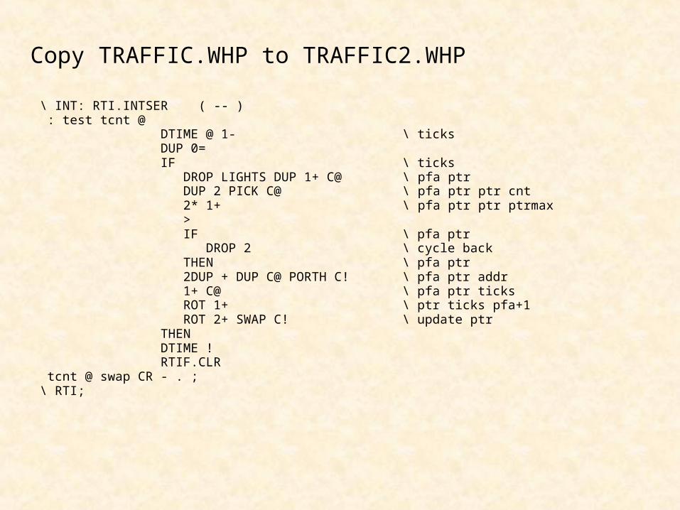
\ INT: RTI.INTSER ( -- ) : test tcnt @ DTIME @ 1- \ ticks DUP 0= IF \ ticks DROP LIGHTS DUP 1+ C@ \ pfa ptr DUP 2 PICK C@ \ pfa ptr ptr cnt 2* 1+ \ pfa ptr ptr ptrmax > IF \ pfa ptr DROP 2 \ cycle back THEN \ pfa ptr 2DUP + DUP C@ PORTH C! \ pfa ptr addr 1+ C@ \ pfa ptr ticks ROT 1+ \ ptr ticks pfa+1 ROT 2+ SWAP C! \ update ptr THEN DTIME ! RTIF.CLR tcnt @ swap CR - . ;\ RTI;
Copy TRAFFIC.WHP to TRAFFIC2.WHP
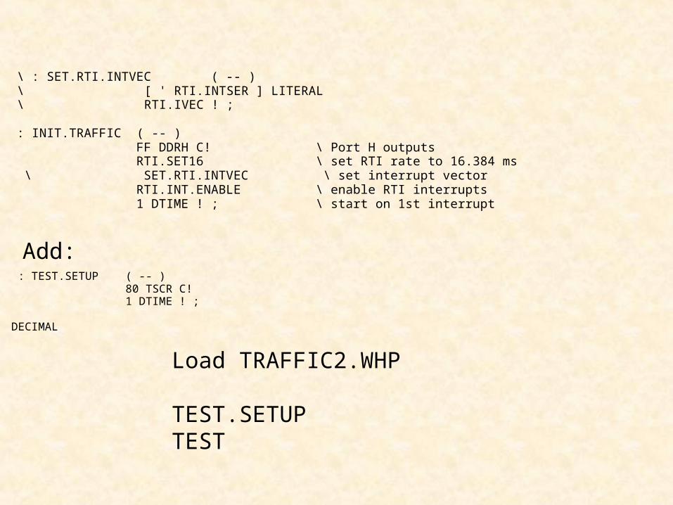
\ : SET.RTI.INTVEC ( -- )\ [ ' RTI.INTSER ] LITERAL\ RTI.IVEC ! ;
: INIT.TRAFFIC ( -- ) FF DDRH C! \ Port H outputs RTI.SET16 \ set RTI rate to 16.384 ms \ SET.RTI.INTVEC \ set interrupt vector RTI.INT.ENABLE \ enable RTI interrupts 1 DTIME ! ; \ start on 1st interrupt
Load TRAFFIC2.WHP
TEST.SETUPTEST
: TEST.SETUP ( -- ) 80 TSCR C! 1 DTIME ! ;
DECIMAL
Add:
Timers
• The 68HC12 Programmable Timer
• Output Compares
• Input Capture
• Pulse Accumulator
• Timing Interrupt Service Routines
• A Circular Queue Data Structure
• Keypad Interfacing Using Interrupts
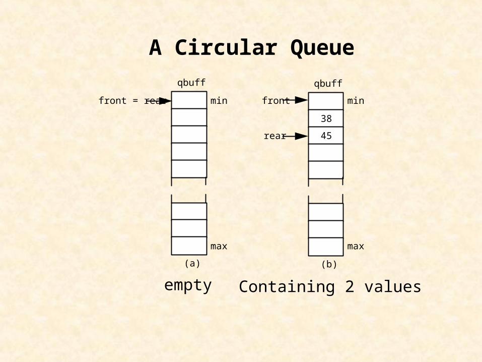
min
max
min
max
front = rear front
rear
38
45
qbuff qbuff
(b)(a)
A Circular Queue
empty Containing 2 values

inc rearif rear > maxthen rear = minif front = rearthen queue is full
dec rearif rear < minthen rear = max
else store value at rear
Figure 10.19 Algorithm to store a value in the circular queue in Figure 10.18
if front = rearthen queue is empty (set false flag)else inc front
if front > max then front = min read byte at front set true flag
Figure 10.20 Algorithm to check queue for a value
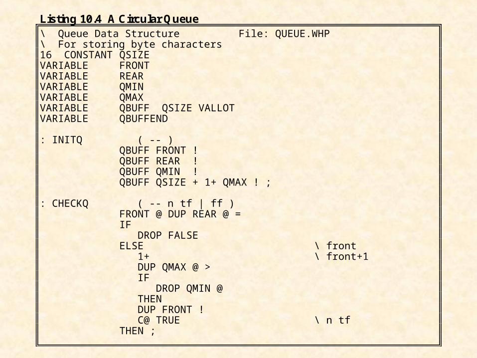
Listing 10.4 A Circular Queue\ Queue Data Structure File: QUEUE.WHP\ For storing byte characters16 CONSTANT QSIZEVARIABLE FRONTVARIABLE REARVARIABLE QMINVARIABLE QMAXVARIABLE QBUFF QSIZE VALLOTVARIABLE QBUFFEND
: INITQ ( -- )QBUFF FRONT !QBUFF REAR !QBUFF QMIN !QBUFF QSIZE + 1+ QMAX ! ;
: CHECKQ ( -- n tf | ff )FRONT @ DUP REAR @ =IF DROP FALSEELSE \ front 1+ \ front+1 DUP QMAX @ > IF DROP QMIN @ THEN DUP FRONT ! C@ TRUE \ n tfTHEN ;
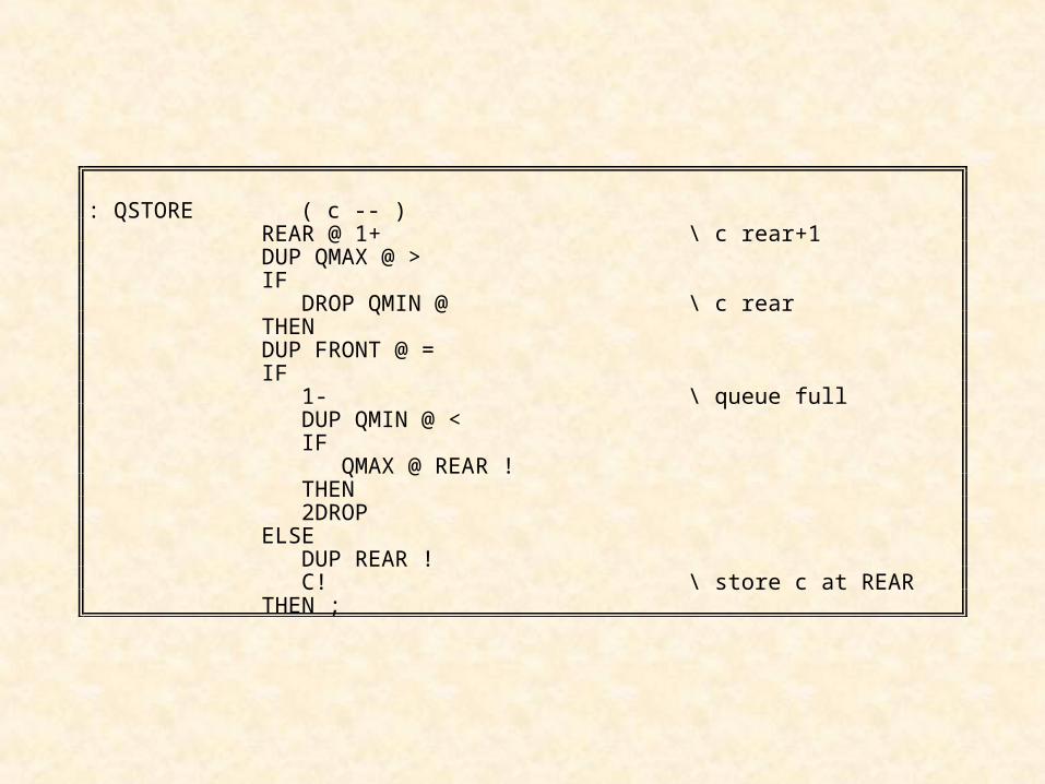
: QSTORE ( c -- )REAR @ 1+ \ c rear+1DUP QMAX @ >IF DROP QMIN @ \ c rearTHENDUP FRONT @ =IF 1- \ queue full DUP QMIN @ < IF QMAX @ REAR ! THEN 2DROPELSE DUP REAR ! C! \ store c at REARTHEN ;
Timers
• The 68HC12 Programmable Timer
• Output Compares
• Input Capture
• Pulse Accumulator
• Timing Interrupt Service Routines
• A Circular Queue Data Structure
• Keypad Interfacing Using Interrupts
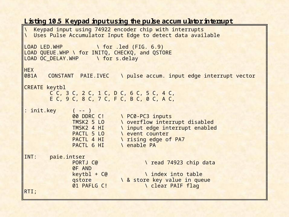
Listing 10.5 Keypad input using the pulse accumulator interrupt\ Keypad input using 74922 encoder chip with interrupts\ Uses Pulse Accumulator Input Edge to detect data available
LOAD LED.WHP \ for .led (FIG. 6.9)LOAD QUEUE.WHP \ for INITQ, CHECKQ, and QSTORELOAD OC_DELAY.WHP \ for s.delay
HEX0B1A CONSTANT PAIE.IVEC \ pulse accum. input edge interrupt vector
CREATE keytbl C C, 3 C, 2 C, 1 C, D C, 6 C, 5 C, 4 C, E C, 9 C, 8 C, 7 C, F C, B C, 0 C, A C,
: init.key ( -- ) 00 DDRC C! \ PC0-PC3 inputs
TMSK2 5 LO \ overflow interrupt disabledTMSK2 4 HI \ input edge interrupt enabledPACTL 5 LO \ event counterPACTL 4 HI \ rising edge of PA7PACTL 6 HI \ enable PA
INT: paie.intser PORTJ C@ \ read 74923 chip data
0F AND keytbl + C@ \ index into table qstore \ & store key value in queue 01 PAFLG C! \ clear PAIF flagRTI;
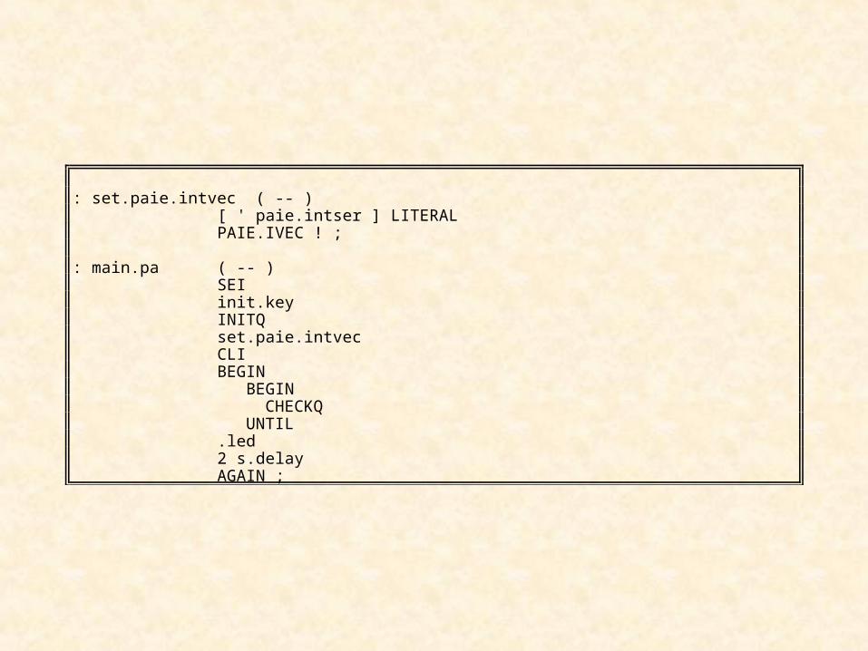
: set.paie.intvec ( -- ) [ ' paie.intser ] LITERAL PAIE.IVEC ! ;
: main.pa ( -- ) SEI init.key INITQ set.paie.intvec CLI BEGIN BEGIN CHECKQ UNTIL .led 2 s.delay AGAIN ;
Timers (cont.)
• Pulse Train Using Interrupts
• Measuring the Period of a Pulse Train Using Interrupts
• The Polaroid Ultrasonic Transducer– An Ultrasonic Tape Measure
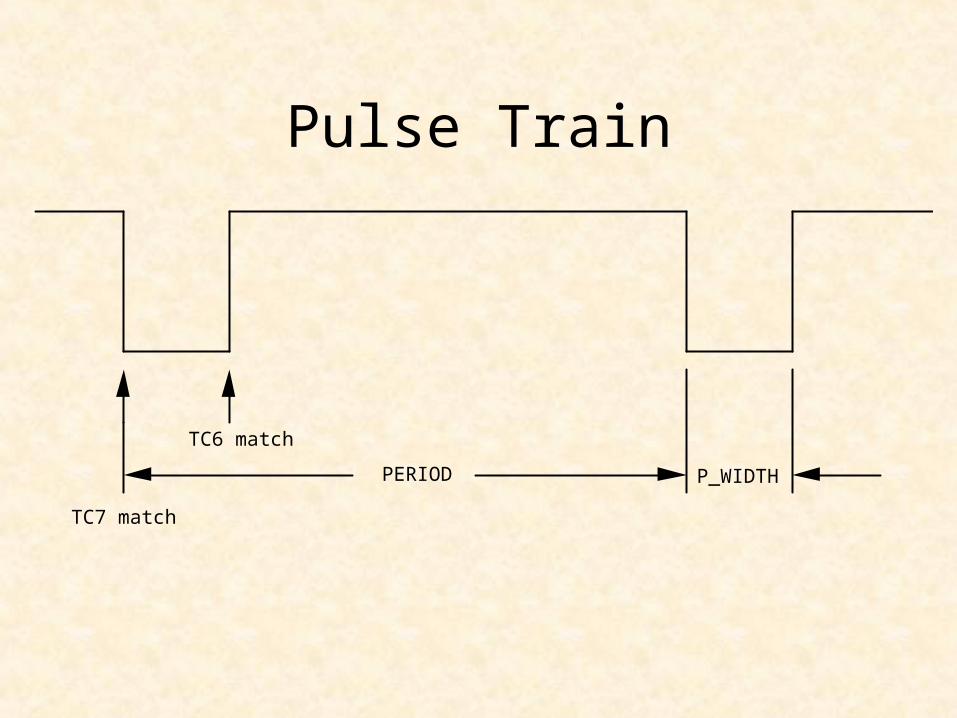
Pulse Train
TC6 match
TC7 match
PERIOD P_WIDTH
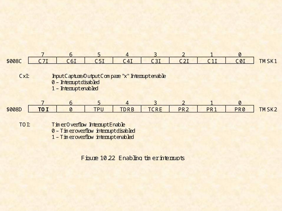
7 6 5 4 3 2 1 0$008C C7I C6I C5I C4I C3I C2I C1I C0I TMSK1
CxI: Input Capture/Output Compare "x" Interrupt enable0 – Interrupt disabled1 – Interrupt enabled
7 6 5 4 3 2 1 0$008D TOI 0 TPU TDRB TCRE PR2 PR1 PR0 TMSK2
TOI: Timer Overflow Interrupt Enable0 – Timer overflow interrupt disabled1 – Timer overflow interrupt enabled
Figure 10.22 Enabling timer interrupts
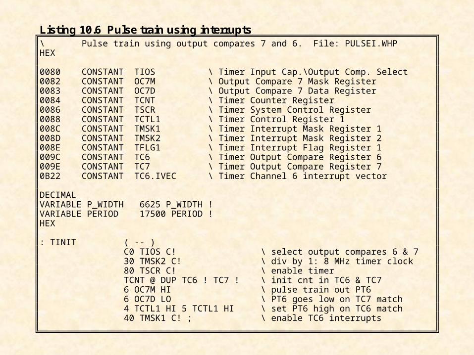
Listing 10.6 Pulse train using interrupts\ Pulse train using output compares 7 and 6. File: PULSEI.WHPHEX
0080 CONSTANT TIOS \ Timer Input Cap.\Output Comp. Select0082 CONSTANT OC7M \ Output Compare 7 Mask Register0083 CONSTANT OC7D \ Output Compare 7 Data Register0084 CONSTANT TCNT \ Timer Counter Register0086 CONSTANT TSCR \ Timer System Control Register0088 CONSTANT TCTL1 \ Timer Control Register 1008C CONSTANT TMSK1 \ Timer Interrupt Mask Register 1008D CONSTANT TMSK2 \ Timer Interrupt Mask Register 2008E CONSTANT TFLG1 \ Timer Interrupt Flag Register 1009C CONSTANT TC6 \ Timer Output Compare Register 6009E CONSTANT TC7 \ Timer Output Compare Register 70B22 CONSTANT TC6.IVEC \ Timer Channel 6 interrupt vector
DECIMALVARIABLE P_WIDTH 6625 P_WIDTH !VARIABLE PERIOD 17500 PERIOD !HEX
: TINIT ( -- ) C0 TIOS C! \ select output compares 6 & 7 30 TMSK2 C! \ div by 1: 8 MHz timer clock 80 TSCR C! \ enable timer TCNT @ DUP TC6 ! TC7 ! \ init cnt in TC6 & TC7 6 OC7M HI \ pulse train out PT6 6 OC7D LO \ PT6 goes low on TC7 match 4 TCTL1 HI 5 TCTL1 HI \ set PT6 high on TC6 match 40 TMSK1 C! ; \ enable TC6 interrupts
: CLR.C76 ( -- ) \ clear both C7F and C6F C0 TFLG1 C! ;
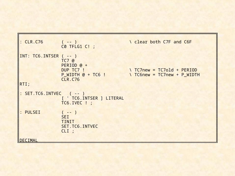
INT: TC6.INTSER ( -- ) TC7 @ PERIOD @ + DUP TC7 ! \ TC7new = TC7old + PERIOD P_WIDTH @ + TC6 ! \ TC6new = TC7new + P_WIDTH CLR.C76RTI;
: SET.TC6.INTVEC ( -- ) [ ' TC6.INTSER ] LITERAL TC6.IVEC ! ;
: PULSEI ( -- ) SEI TINIT SET.TC6.INTVEC CLI ;
DECIMAL

Timers (cont.)
• Pulse Train Using Interrupts
• Measuring the Period of a Pulse Train Using Interrupts
• The Polaroid Ultrasonic Transducer– An Ultrasonic Tape Measure
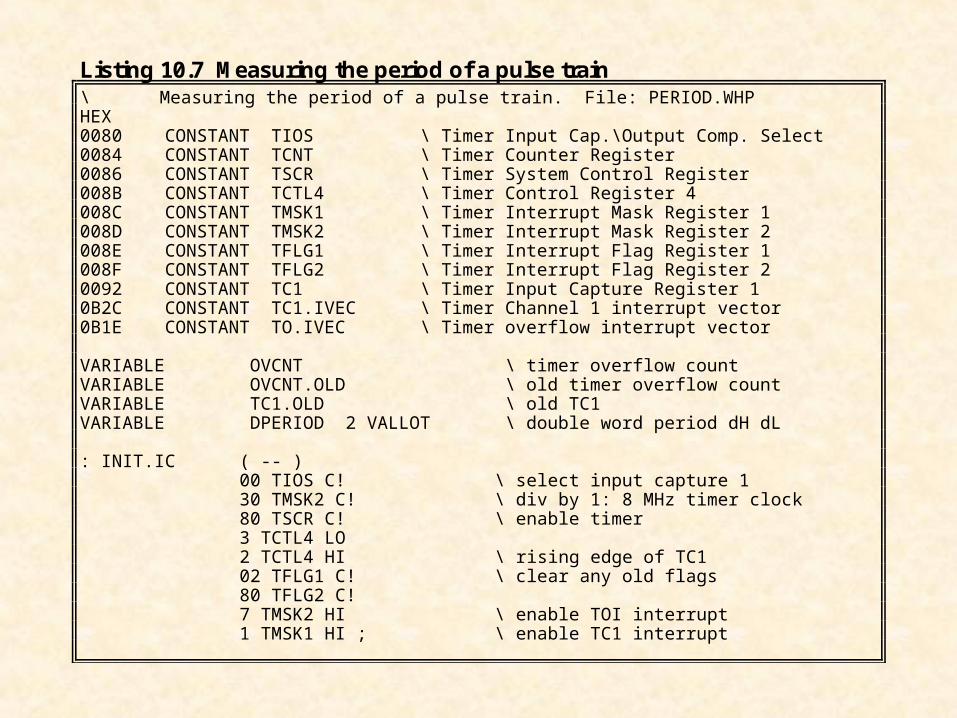
Listing 10.7 Measuring the period of a pulse train\ Measuring the period of a pulse train. File: PERIOD.WHPHEX0080 CONSTANT TIOS \ Timer Input Cap.\Output Comp. Select0084 CONSTANT TCNT \ Timer Counter Register0086 CONSTANT TSCR \ Timer System Control Register008B CONSTANT TCTL4 \ Timer Control Register 4008C CONSTANT TMSK1 \ Timer Interrupt Mask Register 1008D CONSTANT TMSK2 \ Timer Interrupt Mask Register 2008E CONSTANT TFLG1 \ Timer Interrupt Flag Register 1008F CONSTANT TFLG2 \ Timer Interrupt Flag Register 20092 CONSTANT TC1 \ Timer Input Capture Register 10B2C CONSTANT TC1.IVEC \ Timer Channel 1 interrupt vector0B1E CONSTANT TO.IVEC \ Timer overflow interrupt vector
VARIABLE OVCNT \ timer overflow countVARIABLE OVCNT.OLD \ old timer overflow countVARIABLE TC1.OLD \ old TC1VARIABLE DPERIOD 2 VALLOT \ double word period dH dL
: INIT.IC ( -- )00 TIOS C! \ select input capture 130 TMSK2 C! \ div by 1: 8 MHz timer clock80 TSCR C! \ enable timer3 TCTL4 LO2 TCTL4 HI \ rising edge of TC102 TFLG1 C! \ clear any old flags80 TFLG2 C!7 TMSK2 HI \ enable TOI interrupt1 TMSK1 HI ; \ enable TC1 interrupt

\ Timer overflow interrupt routineINT: TO.INTSER ( -- )
1 OVCNT +! \ inc OVCNT80 TFLG2 C! \ clear TOF
RTI;
\ Input capture 1 interrupt routineINT: TC1.INTSER ( -- )
TC1.OLD @ OVCNT.OLD @ \ ic.o ov.oTC1 @ DUP TC1.OLD ! \ ic.o ov.o icOVCNT @ DUP OVCNT.OLD ! \ ic.o ov.o ic ov2SWAP D- \ spL spHDPERIOD 2! \ store period in DPERIOD02 TFLG1 C! \ clear C1F
RTI;
\ Set interrupt vectors: SET.TO.INTVEC ( -- )
[ ' TO.INTSER ] LITERALTO.IVEC ! ;
: SET.TC1.INTVEC ( -- )[ ' TC1.INTSER ] LITERALTC1.IVEC ! ;
\ Main program: MAIN ( -- )
SEI \ set interrupt flagSET.TO.INTVEC \ set interrupt vectorsSET.TC1.INTVECINIT.IC \ init input captureCLI ; \ clear interrupt flag
Timers (cont.)
• Pulse Train Using Interrupts
• Measuring the Period of a Pulse Train Using Interrupts
• The Polaroid Ultrasonic Transducer– An Ultrasonic Tape Measure

Target
Transmitted pulse
Reflected pulse
Transducer
INIT ECHO
4 7
PT6 PT1
68HC12
Ranging Circuit Board VccGND91
Polaroid Ultrasonic Ranging System
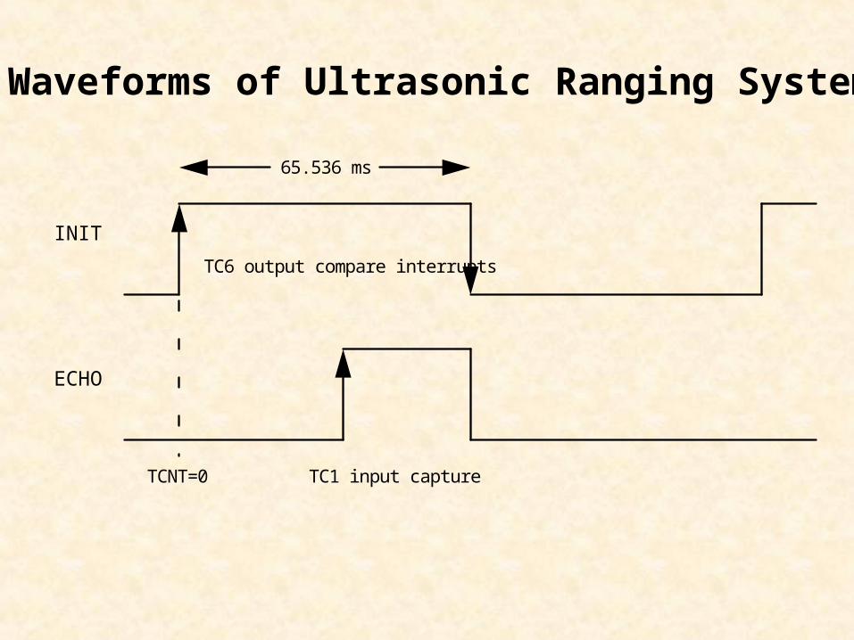
Waveforms of Ultrasonic Ranging System
INIT
ECHO
TCNT=0
65.536 ms
TC1 input capture
TC6 output compare interrupts
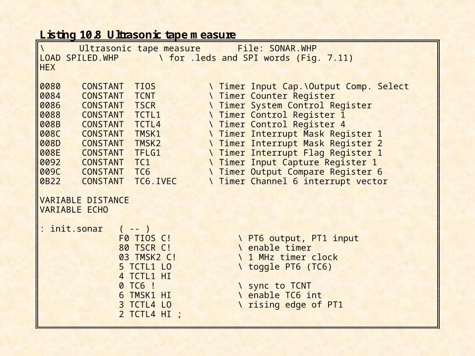
Listing 10.8 Ultrasonic tape measure\ Ultrasonic tape measure File: SONAR.WHPLOAD SPILED.WHP \ for .leds and SPI words (Fig. 7.11)HEX
0080 CONSTANT TIOS \ Timer Input Cap.\Output Comp. Select0084 CONSTANT TCNT \ Timer Counter Register0086 CONSTANT TSCR \ Timer System Control Register0088 CONSTANT TCTL1 \ Timer Control Register 1008B CONSTANT TCTL4 \ Timer Control Register 4008C CONSTANT TMSK1 \ Timer Interrupt Mask Register 1008D CONSTANT TMSK2 \ Timer Interrupt Mask Register 2008E CONSTANT TFLG1 \ Timer Interrupt Flag Register 10092 CONSTANT TC1 \ Timer Input Capture Register 1009C CONSTANT TC6 \ Timer Output Compare Register 60B22 CONSTANT TC6.IVEC \ Timer Channel 6 interrupt vector
VARIABLE DISTANCEVARIABLE ECHO
: init.sonar ( -- )F0 TIOS C! \ PT6 output, PT1 input80 TSCR C! \ enable timer03 TMSK2 C! \ 1 MHz timer clock5 TCTL1 LO \ toggle PT6 (TC6)4 TCTL1 HI0 TC6 ! \ sync to TCNT6 TMSK1 HI \ enable TC6 int3 TCTL4 LO \ rising edge of PT12 TCTL4 HI ;
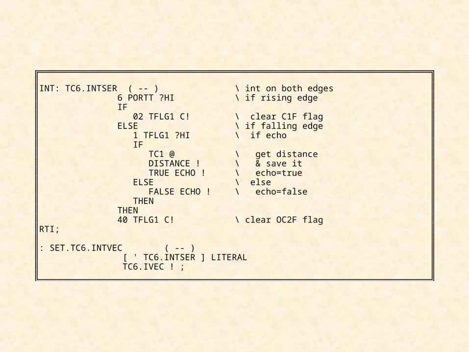
INT: TC6.INTSER ( -- ) \ int on both edges6 PORTT ?HI \ if rising edgeIF
02 TFLG1 C! \ clear C1F flagELSE \ if falling edge 1 TFLG1 ?HI \ if echo IF TC1 @ \ get distance DISTANCE ! \ & save it TRUE ECHO ! \ echo=true ELSE \ else FALSE ECHO ! \ echo=false THENTHEN
40 TFLG1 C! \ clear OC2F flagRTI;
: SET.TC6.INTVEC ( -- ) [ ' TC6.INTSER ] LITERAL TC6.IVEC ! ;
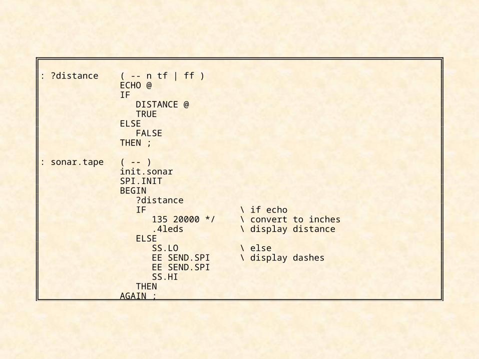
: ?distance ( -- n tf | ff )ECHO @IF DISTANCE @ TRUEELSE FALSETHEN ;
: sonar.tape ( -- )init.sonarSPI.INITBEGIN ?distance IF \ if echo 135 20000 */ \ convert to inches .4leds \ display distance ELSE SS.LO \ else EE SEND.SPI \ display dashes EE SEND.SPI SS.HI THENAGAIN ;
ExercisesExercise 10.6
The TSL245 is an infrared light-to-frequency converter from Texas Instruments thatcan be used to measure light intensity. Its spectral responsivity is above 0.5 forwavelengths between about 850 and 1000 nm with a maximum responsivity at about 920nm. The sensor includes a photodiode and current-to-frequency converter in a singlepackage with three pins: power, ground, and output. The output is a square wave (50%duty cycle) with a frequency (between 1 Hz and 500 KHz) directly proportional to lightintensity. See the web site http://www.ti.com/sc/docs/schome.htm. to download a detaileddata sheet.
a. Write a WHYP word called light1 ( -- n ) that will leave a frequency valuebetween 0 and 65,535 on the data stack which is proportional to the light level.Use an input capture to measure the instantaneous period of the square wave.
b. Write a WHYP word called light2 ( -- n ) that will leave a frequency valuebetween 0 and 65,535 on the data stack which is proportional to the light level.Use the pulse accumulator to count the number of cycles of the square wave thatoccur in a second.
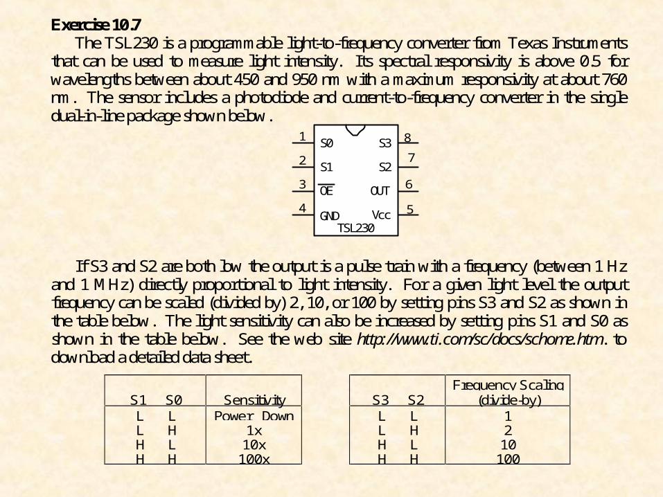
Exercise 10.7The TSL230 is a programmable light-to-frequency converter from Texas Instruments
that can be used to measure light intensity. Its spectral responsivity is above 0.5 forwavelengths between about 450 and 950 nm with a maximum responsivity at about 760nm. The sensor includes a photodiode and current-to-frequency converter in the singledual-in-line package shown below.
1
2
3
4GND
S3S0
S1
OE
S2
OUT
TSL230
5
6
7
8
Vcc
If S3 and S2 are both low the output is a pulse train with a frequency (between 1 Hzand 1 MHz) directly proportional to light intensity. For a given light level the outputfrequency can be scaled (divided by) 2, 10, or 100 by setting pins S3 and S2 as shown inthe table below. The light sensitivity can also be increased by setting pins S1 and S0 asshown in the table below. See the web site http://www.ti.com/sc/docs/schome.htm. todownload a detailed data sheet.
S1 S0 Sensitivity S3 S2Frequency Scaling
(divide-by)L LL HH LH H
Power Down1x10x100x
L LL HH LH H
1210100
Exercise 10.8The ADXL202 from Analog Devices is a ±2 g Dual Axis Accelerometer with Digital
Output. See Exercise 9.5 for a description of the ADXL05 single-axis accelerometer withanalog output. The ADXL202 uses a similar technology as the ADXL05 for each of twoperpendicular axes. The output for each axis is a pulse train in which the duty cycle isproportional to the acceleration. The device comes in a 14-pin DIP with the x-axis ofacceleration along the length of the chip with the y-axis perpendicular to x in the plane ofthe chip. You can go to http://www.analog.com/product/Product_Center.html todownload a complete data sheet.
The period of the output waveform for both channels is determined by a single resistorRset. The period, T2, given by Rset()/125 M, is typically between 0.5 ms and 10 ms.The high time of the pulse train is T1. A duty cycle of 50% (T1 = 0.5 x T2) correspondsto 0 g. The acceleration is given by
A(g) = (T1/T2 - 0.5)/12.5%Write a WHYP word called get.xyg ( -- x y ) that will leave the accelerations along the
x- and y-axes, in milli-g, on the data stack. That is, a value of 1000 corresponds to 1 g.

Exercise 10.9The ADXL202 described in Exercise 10.8 can be used to measure dual-axis tilt by
measuring the component of the earth's gravity. If the x and y axes of the ADXL202 areboth oriented parallel to the earth's surface (i.e. horizontal) then the output duty cycle ofboth will be 50% (0 g). A tilt of the ADXL202 will produce an x-acceleration, Ax, and ay-acceleration, Ay, that can be measured using the formula given in Exercise 10.8. Fromthese measured values between -1 g and +1 g the angles, pitch and roll, can be computedfrom
pitch = arcsin(Ax/1 g)roll = arcsin(Ay/1 g)
Write a WHYP word called tilt ( -- pitch roll ) that will leave the tilt angles, pitch androll, in tenths of a degree, on the data stack. Hint: Use the arcsin table in Figure 5.33 andlinearly interpolate to the nearest tenth of a degree.
Exercise 10.10The ADXL202 described in Exercises 10.8 and 10.9 can be used to measure 360° of
tilt by orienting the chip on a vertical plane. For example, if the x-axis is vertical (pointingdown toward the earth's surface) and the y-axis is horizontal (parallel to the earth'ssurface) then the x-acceleration will be -1 g and the y-acceleration will by 0 g. As the chipis rotated in the vertical plane the x-acceleration will increase toward zero and the y-acceleration will increase toward +1 g. In fact, as the chip is rotated through 360° theaccelerations Ax and Ay will vary as sinusoidal quadrature signals of the type shown inFigure 8.10 where B corresponds to the x-acceleration curve and A corresponds to the y-acceleration curve.
Write a WHYP word called wheel ( -- angle ) that will measure the x- and y-accelerations of an ADXL202 mounted on the surface of a wheel and leave the orientationof the wheel (0 - 360° ) on the data stack.
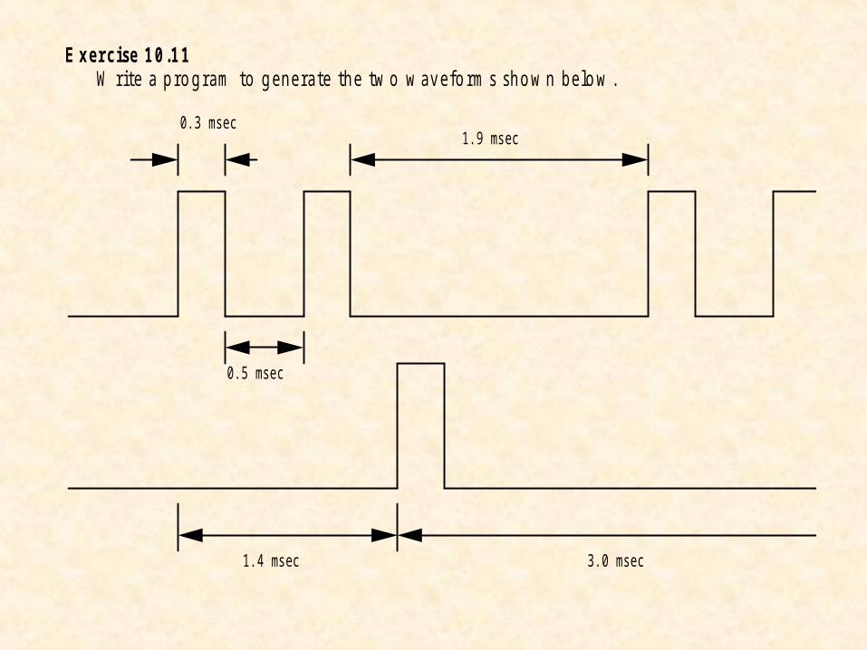
E x e r c i s e 1 0 . 1 1W r it e a p r o g r a m t o g e n e r a t e t h e t w o w a v e fo r m s s h o w n b e lo w .
0.3 msec
0.5 msec
3.0 msec
1.9 msec
1.4 msec
Exercise 10.12Motor speeds can be measured using a Hall effect sensor. A Hall effect switch
produces a digital output that goes low when the south pole of an external magnet is closeto the sensor and goes high when the magnet is removed. An internal magnet Hall effectspeed sensor provide a digital output pulse when gear or thread teeth move past thesensor. See the web site http://www.sensorsolutionscorp.com/ for more information onHall effect sensors.
a. Assume a single magnet is mounted on a wheel connected to the shaft of a motor.Write a WHYP word called RPM ( -- n ) that will measure the speed of the motorin RPM using a Hall effect switch.
b. Assume that a wheel has eight teeth evenly spaced on its circumference. Write aWHYP word called SPEED ( -- n ) that will measure the speed of the motor inRPM using a Hall effect speed sensor.

Exercise 10.13Incremental optical encoders can be used to measure the direction and angle through
which a shaft is rotated. A typical incremental encoder will have two square wave outputs(channels A and B) that are in phase quadrature. If the shaft is rotating clockwise, thenthe square wave from channel B will lead channel A by 90degrees. On the other hand ifthe shaft is rotating counter-clockwise, then the square wave from channel A will leadchannel B by 90 degrees. See the web site http://www.opticalencoder.com/ for moreinformation on incremental optical encoders.
Assume you have an incremental optical encoder with 360 counts per revolution thatis connected to a dial that can move from 0 to 360 degrees. Write a program that willmeasure the angle of the dial at any time. You must initialize the count to zero when thedial is at 0 degrees and then keep track of both positive and negative counts.
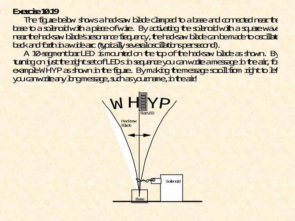
Exercise 10.19The figure below shows a hacksaw blade clamped to a base and connected near the
base to a solenoid with a piece of wire. By activating the solenoid with a square wavenear the hacksaw blade's resonance frequency, the hacksaw blade can be made to oscillateback and forth in a wide arc (typically several oscillations per second).
A 10-segment bar LED is mounted on the top of the hacksaw blade as shown. Byturning on just the right set of LEDs in sequence you can write a message in the air, forexample WHYP as shown in the figure. By making the message scroll from right to leftyou can write any long message, such as your name, in the air!
Solenoid
Base
Bar LED
Hacksaw Blade
H Y
Recommended