International Journal of Modern Physics and Applications
Vol. 1, No. 4, 2015, pp. 193-199
http://www.aiscience.org/journal/ijmpa
* Corresponding author
E-mail address: [email protected]
Thin Film Deposition Processes
Dler Adil Jameel1, 2, *
1School of Physics and Astronomy, Nottingham Nanotechnology and Nanoscience Center University of Nottingham, Nottingham, United Kingdom
2Department of Physics, Faculty of Science, University of Zakho, Duhok, Kurdistan Region, Iraq
Abstract
During the last many decades the methods of forming thin films materials have increased significantly. In general, thin film is a
small thickness that produces by physical vapour deposition (PVD) and chemical vapour deposition (CVD). Despite the PVD
technique has a few drawbacks, it remains an important method and more beneficial than CVD technique for depositing thin
films materials. This project examines some remarkable similarities and differences between PVD and CVD systems as well as
evaluates the different techniques of depositing thin film. The majority of researchers have attempted to explain and justify the
most precise system for depositing thin film since it is important in several applications such as surgical/medical and automotive.
It is concluded that the most efficient method of depositing is PVD process. In addition, it has been found that there are more
differences than similarities between PVD and CVD processes.
Keywords Thin Film, Physical Vapour Deposition (PVD), and Chemical Vapour Deposition (CVD)
Received: July 2, 2015 / Accepted: August 9, 2015 / Published online: August 17, 2015
@ 2015 The Authors. Published by American Institute of Science. This Open Access article is under the CC BY-NC license.
http://creativecommons.org/licenses/by-nc/4.0/
1. Introduction
Over the past approximately two centuries, there has been
significantly changing thin film deposition process. Indeed,
Fraunhofe first observed generating of thin film layer over 195
years ago on the surface of glass (ETAFILM Technology Inc,
n.d). According to Wasa, Kitabatake and Adechi (2004), a thin
film is a small-dimensional material on the substrate produced
by intensifying, one-by-one, and ionic/molecular/atomic
species of matter. The thickness of thin film is generally less
than a number of microns. In fact, there is another type of film
that is called thick film, which is known as a
small-dimensional material formed by accumulating great
grains/aggregates/clusters of ionic/molecular/atomic species
or thinning a three-dimensional material.
Factually, over the past 50 years, the thin films have been used
for manufacturing optical coatings, electronic devices,
decorative parts, and instrument hard coatings. The thin film is
a conventional well-established material technology. In
contrast, since the thin film technology is a main improvement
of novel materials such as nanometre materials in the
twenty-first century, it is still being developed on a daily basis
(Wasa, Kitabatake and Adechi, 2004).
On the other hand, in the present time, the deposition process
is classified into two types systems physical vapour deposition
(PVD) and chemical vapour deposition (CVD), depending on
the different principle causing film deposition. The first
technique PVD is split into two classes thermal evaporation
and sputtering; the second one CVD method is divided into
plasma enhanced chemical vapour deposition (PECVD), laser
chemical vapour deposition (LCVD), and metal organic
chemical vapour deposition (MOCVD) (Singh and
Shimakawa, 2003, and Pathan, 2004).
The aim of this project is to illustrate similarities and
differences between two types of deposition process, which
are physical vapour deposition (PVD) and chemical vapour
deposition (CVD), for producing thin film material on the
substrate. In addition, the purpose of this paper is to evaluate

194 Dler Adil Jameel: Thin Film Deposition Processes
the most favourable methods of deposition process of thin film.
Firstly, this project will not only provide a brief overview of
physical vapour deposition and its types that are thermal
evaporation and sputtering, but also explain advantages and
disadvantages of PVD system in section one. Moreover, it will
explain briefly only one method of the chemical vapour
deposition, which is called plasma enhanced chemical vapour
deposition (PECVD). Furthermore, the advantages and
disadvantages of CVD system will then be examined in
section two. Finally, will demonstrate compare and contrast
the two processes in unit three.
2. Physical Vapour Deposition (PVD)
Freund (2003) claims that the physical vapour deposition,
which is one of the approaches to fabricate thin film materials
on the substrate, is a system that the physical processes occur
through it such as evaporation, collision of ions or sublimation
on a target, the transfer of atoms from a solid or molten source
onto a substrate easily.
Generally, the PVD processes are performed under vacuum
circumstances, and it is involved four steps. Firstly,
evaporation, over this stage the target is evaporated by high
energy source such as resistive heating or electrons beam.
Secondly, transportation, the vaporized atoms move from
target to the surface of substrate through this phase. The third
step is reaction, in some cases deposition, if there is a gas such
as nitrogen or oxygen in the system, the atoms of materials
reacts with the gas. If, however, in cases where the coating
does not contain of gas, but it only consist of the target
material, this phase does not be part of the process. Finally,
deposition, through this stage the surface of substrate will be
built. This technique is classified into two sorts, thermal
evaporation and sputtering (AZoM 2002, and Korkin el al
2007).
2.1. Thermal Evaporation
Reference to Wasa, Kitabatake and Adechi (2004) reveal that
the process of thermal evaporation, which is traditionally
known as vacuum deposition, is used as a simplest technique
for preparing thin film with a small number of micrometre
(µm) thicknesses. The thermal evaporation process consists of
evaporating and condensing processes in a vacuum (≈1×10⁻⁵
millibar) chamber. Firstly, source materials are evaporated by
the heated source, which is maintaining a few cm distances
from a substrate. Then, evaporated particles are condensed on
the substrate. This process can use two types of sources that
are resistive and electron beam source, which are shown in
Figure (1).
Figure (1). Types of thermal evaporation process.
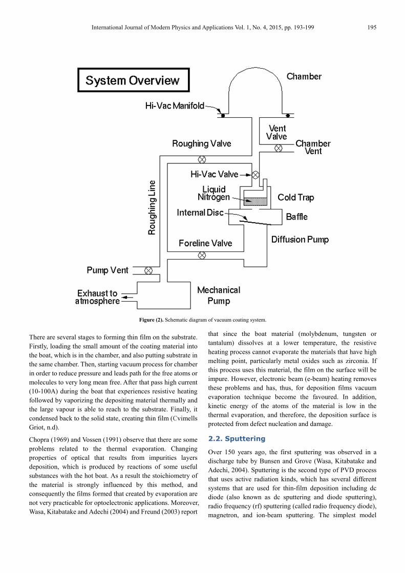
The vacuum coating system shown in Figure (2) consists of
mechanical rotary pump that is used to evacuate the chamber
through the roughing line from atmospheric pressure to a level
at, and diffusion pump which can be utilized as a primary
pump to maintain the pressure in the chamber less than 5×10⁻²
millibar, and a high diffusion pump to conserve the pressure to
less than 5×10⁻⁵
millibar through the diffusion line (Chopra,
1969).
The resistive method consists of heating materials with a
resistively heated boat or filament, usually manufactured of
refractory metals such as tungsten, molybdenum and tantalum
with or without ceramic coating (Chopra, 1969).
International Journal of Modern Physics and Applications Vol. 1, No. 4, 2015, pp. 193-199 195
Figure (2). Schematic diagram of vacuum coating system.
There are several stages to forming thin film on the substrate.
Firstly, loading the small amount of the coating material into
the boat, which is in the chamber, and also putting substrate in
the same chamber. Then, starting vacuum process for chamber
in order to reduce pressure and leads path for the free atoms or
molecules to very long mean free. After that pass high current
(10-100A) during the boat that experiences resistive heating
followed by vaporizing the depositing material thermally and
the large vapour is able to reach to the substrate. Finally, it
condensed back to the solid state, creating thin film (Cvimells
Griot, n.d).
Chopra (1969) and Vossen (1991) observe that there are some
problems related to the thermal evaporation. Changing
properties of optical that results from impurities layers
deposition, which is produced by reactions of some useful
substances with the hot boat. As a result the stoichiometry of
the material is strongly influenced by this method, and
consequently the films formed that created by evaporation are
not very practicable for optoelectronic applications. Moreover,
Wasa, Kitabatake and Adechi (2004) and Freund (2003) report
that since the boat material (molybdenum, tungsten or
tantalum) dissolves at a lower temperature, the resistive
heating process cannot evaporate the materials that have high
melting point, particularly metal oxides such as zirconia. If
this process uses this material, the film on the surface will be
impure. However, electronic beam (e-beam) heating removes
these problems and has, thus, for deposition films vacuum
evaporation technique become the favoured. In addition,
kinetic energy of the atoms of the material is low in the
thermal evaporation, and therefore, the deposition surface is
protected from defect nucleation and damage.
2.2. Sputtering
Over 150 years ago, the first sputtering was observed in a
discharge tube by Bunsen and Grove (Wasa, Kitabatake and
Adechi, 2004). Sputtering is the second type of PVD process
that uses active radiation kinds, which has several different
systems that are used for thin-film deposition including dc
diode (also known as dc sputtering and diode sputtering),
radio frequency (rf) sputtering (called radio frequency diode),
magnetron, and ion-beam sputtering. The simplest model

196 Dler Adil Jameel: Thin Film Deposition Processes
among these sputtering systems is the dc diode (Mattox, 2003
and Freund, 2003). Vossen (1991) points out that the atoms in
the process of sputtering generally are evicted from surfaces
of source commonly preserved at room temperature, during
the influence of gaseous ions. It means that sputtering is the
technology that is where the release of material from the
source at a temperature much lower than the evaporation.
The system of dc diode is formed of vacuum chamber, power
supply (high voltage), and two planar electrodes cathode and
anode as shown in Figure (3). This system connects with the
vacuum system to evacuate the chamber (Wasa, Kitabatake
and Adechi, 2004, and Freund, 2003).
Figure (3). Dc diode system (Wasa, Kitabatake and Adechi, 2004: 40).
The source material, called target, is placed in the vacuum
chamber on the cathode plate with the substrate locates on the
anode plate, and fills with sputtering gas such as argon gas
(Ar), which is an inert gas, at low pressure (4×10⁻²
torr) (Wasa,
Kitabatake and Adechi, 2004, and MEMSnet, n.d). In this type
of system of deposition, ions of argon (Ar+) that produced in
the radiance discharge are accelerated at high speed by an
imposed electric field toward the cathode (target), and sputter
the target, resulting in the thin films deposition on the
substrates (Wasa, Kitabatake and Adechi, 2004, and Freund,
2003).
As Freund (2003) and SiliconFarEast (2004) point out, one of
the main advantages of sputtering process is that control in
preserving stoichiometry and regularity of film thickness is
better than in evaporation process, and there is a flexibility of
fundamental deposition of any amorphous and crystalline
materials. Moreover, sputter deposition, for polycrystalline
films, produces the film grain structure that has typically many
crystallographic orientations without preferred texture.
However, kinetic energy of sputtered atoms in sputter
deposition is higher than that of atoms in the evaporative
deposition because of the argon gas (Ar) existence in the
sputtering system. Therefore, the surface of deposition in
sputtering process exhibits more damage and defect
nucleation than in thermal evaporation. In addition, a
concentration of impurity atoms of sputtered-deposited films
is greater than thermal-deposited films. Furthermore, Grain
size of the sputtered films is typically smaller than that of the
films deposited by evaporation.
Based on the advantages and disadvantages of sputter and
evaporation process, it can be seen that the thermal
evaporation technique is more favourable than sputtering
technique for depositing thin film for many materials that low
and high melting materials, especially, metals.
2.3. Advantages and Disadvantages of PVD
Process
Nothing is ever perfect; everything has negative and positive
effects. It is undoubtedly true to say that although PVD
process plays an important role in many fields, it has some
obvious drawbacks. One of the significant advantages of using
PVD process is that this process makes it possible for
materials to deposit with developed properties compared to
the substrate material. For instance, these techniques are
commonly used to increase oxidation resistance, hardness and
resistance of wear. As a result, it uses in a several of
applications such as automotive, aerospace, surgical/medical,
dies and shapes for all types of material processing, cutting
tools and fire arms. Moreover, the PVD process enables
approximately any type of inorganic material to use as well as
certain categories of organic materials. In addition, it is
environmentally approachable further than processes such as
electroplating.
On the other hand, one of the important disadvantages is that
the PVD technique requires appropriate cooling system for
some processes operate at high vacuums and temperatures
such as evaporate materials that has high melting point, and
this system not only need skilled operators, but also demands
high capital cost. In addition, frequently the rate of coating
deposition is fairly slow; it is enormously difficult to coat
similar surface and undercuts (AZoM, 2002).
In conclusion, it is important to note that even though there are
some drawbacks associated with PVD process, particularly,
slowing of rate of coating deposition and cost of existence of
appropriate cooling systems, the benefits probably outweigh
the disadvantages, especially as regards with increasing
oxidation resistance, hardness and resistance of wear. As a
consequence, the PVD is more preferable method than CVD,
which will be focused in the next part, for depositing thin film
for many materials as well as useful in wide range of
applications such as automotive, aerospace and
surgical/medical.

International Journal of Modern Physics and Applications Vol. 1, No. 4, 2015, pp. 193-199 197
3. Chemical Vapour Deposition (CVD)
Choy (2003) reports that chemical vapour deposition is a
technique whereby chemical processes such as chemical
reaction at the substrate surface or in the surrounding of the
substrate. According to Bhat (2006), in formal terms, CVD
may be defined as a system in which a combination of gases
reacts with the substrate surface at a relatively great
temperature, leading to decay of certain of the constituents of
the gas combination and the fabrication of a solid film of
depositing of a metal or composite on the substrate. In fact,
there are many sorts of CVD process, but this project is
intending to explain only one significant of them, which is
plasma enhanced chemical vapour deposition (PECVD).
3.1. Plasma Enhanced Chemical Vapour
Deposition (PECVD)
Plasma enhanced chemical vapour deposition (PECVD) is
defined as a glow discharge chemical vapour deposition that is
primarily utilized for the depositing of dielectric film and
passivation films such as nitride or silicon oxide layers at low
temperature. Electron energy (plasma) or heated gas
introduces the necessary energy not only for the chemical
reaction, but also to make it possible for coating to occur at a
low temperature and at a sensible rate (Pathan, 2004 and Choy,
2003).
In general, there are several steps in this technique to produce
thin film as shown in Figure (2-1). Firstly, providing electrical
power at an adequately great voltage to a gas at decreased
pressures, consequences the avalanching of the gas then
produces glow discharge plasma involving of ions, electrons
and electronically excited species. Furthermore, electron
affect ionize and dissociate the vapour reactants, and thus
producing chemically energetic ions and radicals that
undertake the heterogeneous chemical interaction at or close
the heated substrate surface and coat the thin film. Although
the temperature of the vapour reactants may continue close
room temperature, the temperature of the electron can be
approximately 20,000 K or higher, depending on the pressure
at that the discharge is functioned (Choy, 2003 and Vossen,
1991].
Vossen (1991) also points out one of the significant
advantages of PECVD system is that the deposition can occur
on large areas at relatively low temperatures. In addition, it
enables the microstructure deposition of film to be controlled
separately. However, one of the main disadvantages of this
process is that the film does not have high purity. Moreover,
this technique is usually more expensive than other systems.
Figure (4). Plasma enhanced chemical vapour deposition (PECVD) (Choy, 2003: 113).
Based on the advantages and disadvantages of PECVD, it
could be clearly seen that this method is more favourable than
other CVD techniques for depositing thin film for many
materials, particularly, dielectric films.
3.2. Advantages and Disadvantages of CVD
Process
The system of CVD as mentioned in introduction, it has
positive and negative aspects. The main benefit of using this

198 Dler Adil Jameel: Thin Film Deposition Processes
system is that it can control structure of crystal and generate
uniform films with pure materials and high density. Moreover,
CVD system has ability to form film with good clone and
adhesion at sensibly great deposition rates. However, this
method cannot control stoichiometry of films using more than
one material because different materials have different
evaporation rates (Choy, 2003).
4. Compare and Contrast PVD and CVD Process
Pathan (2004), Choy (2003) and Freund (2003) found that
there are several similarities and differences between Physical
vapour deposition (PVD) and chemical vapour deposition
(CVD) systems. Firstly, the system of vacuum of PVD and
that of CVD are similar. They have vacuum chamber, rotary
pump to produce low vacuum, and diffusion pump to acquire
high vacuum. However, usually PVD process works under
high vacuum, while CVD works under low vacuum.
Secondly, as far as temperature is concerned, the most
remarkable similarity between PVD and CVD techniques is
that the temperature of deposition in both systems is generally
more than 150 °C. In contrast, PVD coating is deposited
between 250°C and 450°C, whereas, CVD coating is
deposited at high temperatures in the range of almost 450 C to
roughly 1050°C.
Finally, in CVD, the material introduces in gaseous form onto
the substrate, but it introduces in solid form in PVD. On the
other hand, the gaseous molecules react with substrate in CVD,
whereas the atoms are moving and depositing on the substrate
in PVD.
Overall, it would appear that PVD and CVD systems are quite
different in terms of temperature and degree of vacuum.
5. Conclusion
Over the last 195 years, the processes of depositing thin films
materials have been considerably developing. Generally, there
is not only physical vapour deposition system to produce thin
film, but there is also chemical vapour deposition. In this
project, several important aspects and techniques about thin
film deposition process have been presented such as a brief
overview of PVD process, types of PVD system that are
thermal evaporation and sputtering, a brief overview of CVD
process, PECVD that is a significant technique of CVD, and
advantages and disadvantages of both systems. Finally,
compare and contrast PVD and CVD have been discussed.
From explanation of thin film deposition processes that are
PVD and CVD. It can be concluded that the thermal
evaporation technique, particularly which has electron beam
source, is the most favourable methods for depositing thin
film for materials that have high and low melting. By contrast,
sputtering method is useful for depositing thin film for
polycrystalline. On the other hand, for dielectric films the
PECVD system is more beneficial than other CVD systems.
Moreover, according to the many research, it can be seen that
PVD is more favourable than CDV technique for fabricating
thin film.
In discussion of compare and contrast PVD and CVD process,
it was concluded that the main similarities between two
processes are vacuum system and temperature of deposition.
However, the level of vacuum and degree of temperature of
each system are rather different. In contrast, the most
remarkable difference is the form of introducing materials. For
instance, the form of introducing material on to the substrate
in PVD and CVD is solid and gaseous form, respectively. It
would seem that PVD and CVD are slightly similar.
Acknowledgement
The author would like to thank the ministry of higher
education and scientific research of Kurdistan-Iraq, and also
the University of Zakho for supporting this project.
References
[1] AZoM (2002) Physical Vapour Deposition (PVD) - An Introduction
[2] Physical vapour Deposition (PVD)– An Introduction [online] available from <http://www.azom.com/article.aspx?ArticleID=1558> [29 July 2012]
[3] Bhat, D. G. (2006) ‘Chemical Vapour Deposition’. In Coatings Technology Handbook. ed. by Tracton, A. A. 3rd edn. USA (City not mentioned): Taylor & Francis Group, LLC
[4] Chopra, K. L. (1969) Thin Film Phenomena. New York: McGraw-Hill
[5] Choy, K. L. (2003) Chemical vapour deposition of coatings. London: Elsevier Science Ltd.
[6] Cvimells Griot (n.d) Thin–film production [online] available from <https://www.cvimellesgriot.com/products/Documents/TechnicalGuide/Optical-Coatings.pdf> [28 July 2012]
[7] ETAFILM Technology Inc (n.d) Optical Thin Film Deposition Technology History–Thermal evaporation [online] available from <http://www.etafilm.com.tw/Thinfilm_filter_Deposition_History.html> [25 July 2012]
[8] Freund, L. B., and Suresh, S. (2003) Thin Film Materials. Cambridge: Cambridge University Press
[9] Jameel, D. (2008) X-Ray Diffraction and DC Electrical Conductivity for Te61.8Se38.2 Thin Films. Unpublished MSc thesis. Duhok: University of Duhok

International Journal of Modern Physics and Applications Vol. 1, No. 4, 2015, pp. 193-199 199
[10] Korkin, A., Gusev, E., Labanowski, J., and Luryi, S. (2007) Nanotechnology for Electronic Materials and Devices. New York USA: Springer Science+Business Media, LLC
[11] MEMS net (n. d) Thin Film Deposition Processes [online] available from <http://www.memsnet.org/mems/processes/deposition.html> [01 August 2012]
[12] Pathan, H. M., and Lokhande, C. D. (2004) ‘Deposition of metal chalcogenide thin films by successive ionic layer adsorption and reaction (SILAR) method’. Bull. Mater. Sci. 27 (2), 85-111
[13] SiliconFarEast (2004) Physical Vapour Deposition (PVD) by Sputtering [online] available from <http://www.siliconfareast.com/sputtering.html> [26 July 2012]
[14] Singh, J., and Shimakawa, K. (2003) Advances in Amorphous Semiconductors. London and New York: Taylor & Francis.
[15] Vossen, J. L. (1991) Material Science of Thin Films. 2nd edn. New Jersey: Milton Ohring
[16] Wasa, K., Kitabatake, M., and Adechi, H. (2004) Thin Film Materials Technology. United States: WalliamAndrew, Inc and Springer
Recommended