THERMAL AND MECHANICAL ISOLATION OF OVENIZED MEMS RESONATOR
A DISSERTATION SUBMITTED TO THE DEPARTMENT OF
MECHANICALENGINEERING AND THE COMMITTEE ON GRADUATE STUDIES OF
STANFORD UNIVERSITY IN PARTIAL FULFILLMENT OF
THE REQUIREMENTS FOR THE DEGREE OF DOCTOR OF PHILOSOPHY
Chandra Mohan Jha
December 2008

ii
© Copyright by Chandra Mohan Jha 2008 All Rights Reserved
iii

iv
v
Abstract
Micromechanical silicon resonators are becoming an interesting and viable technology
as a replacement for quartz crystals for timing and frequency reference applications. For
high precision applications in industry and military, oven controlled resonators are used
to compensate for the temperature dependence of resonator frequency. An oven
controlled resonator requires a good temperature sensor and an efficient heater (oven).
However, an external temperature sensor leads to thermal lag and the ovenization leads
to power consumption.
This work presents a silicon micromechanical resonator based digital temperature
sensing technique as well as an efficient local-thermal-isolation method. The
micromechanical resonator based thermometry results into a lag-free temperature sensor
for self temperature compensation suitable for high precision oven control of the
resonator. The thermal isolation technique includes the design of an integrated heater
with the micromechanical resonator such that the mechanical suspension, electrical
heating and thermal isolation are provided in a single compact structure. This results in
reducing the power consumption by more than 20x and the thermal time constant by
more than 50x. Further reduction in power consumption requires analysis of the
resonator structure to maintain its mechanical integrity. An improved thermally isolated
design using topology optimization is described. The final design provides both the
thermal isolation as well as the mechanical isolation with the overall reduction in power
consumption of 40x. Furthermore, these methods are simple enough to implement it
into any existing MEMS fabrication process.

vi

vii
To my sons Arvin and Tatsat

viii
ix
Acknowledgements
This thesis would not have been possible without the important contributions of so
many people I came across during the course of my research work at Stanford. Their
support and guidance not only helped me to complete my research but also transformed
my life and made me who I am today. I would like to take this opportunity to
acknowledge and thank them.
First and foremost, I would like to thank my advisor Prof. Tom Kenny for his
invaluable support and guidance. He is a role model and a perfect mentor for me. I still
remember my first meeting with him, after which I realized that I have to go a long way
and I need a mentor like him. His constant support and encouragement made me
capable enough to overcome many obstacles that came my way, even during tough
times of my illness. I wish I can become a Professor and a Guide like him one day.
I would also like to thank my co-advisors Prof. Ken Goodson and Prof. Ellen Kuhl, who
also accepted to become my reading committee members. Prof. Ken has been an
inspiration for me to learn something new and in-depth in Heat Transfer. I was enrolled
in two of his courses “Fundamentals of Heat Conduction” and “Micro Heat Transfer”
both of which were among the most useful courses for me. Prof. Ellen has been an
extremely supportive and encouraging Guide to me. Her advice and mentorship on
“Topology Optimization” was very important and crucial for my research work. She has
been an extremely motivating and collaborating advisor. I hope I can collaborate with
her to do some path-breaking research sometime in future.
I would also like to thank Prof. Roger Howe and Dr. Rob Candler who have given
guidance at different times of my graduate career at Stanford and took their precious
x
time to serve on my orals committee. I have also benefited from the guidance of John
Vig, and I would like to thank him for that.
The most enriching experience of my research work was the collaboration and
friendship of the members of the Kenny Research Group, past and present. I would like
to thank all of them specially Dr. Matt Hopcroft who helped me throughout my
research. As a senior Kenny Group member, he guided me with all aspects of the
research lab when I joined the group. He helped me in the design, fabrication and the
testing of the device. In fact, one of his resonator designs became very crucial for the
completion of my research work. I had the great pleasure to work with extremely
talented and brilliant people like Renata Melamud, Saurabh Chandorkar, Vipin
Vitikkate, Kuanlin Chen, Jim Salvia, Hyungkyu Lee, Wes Smith, Violet Qu, Andrew
Graham, Matt Messanna, Gaurav Bahl, Shasha Wang, Suhrid Bhat, Shingo Yoneoka,
Jen Bower, Ginel Hill, Hyeun-su Kim, Kevin Lohner, Dan Soto, Yoonjin Won, Cathy,
Mandy and Jim Cybulski, Evelyn Wang, and Holden Li, Michael Bartsch, Woo-tae
Park, Matt Hopcroft, Bongsang Kim, Manu Agarwal, Harsh Mehta, and probably many
more.
Finally, I would like to express my special regards for my family and friends for their
continuous love and support. I wish to thank my parents, my brother, my sister and my
wife Shikha for their unyielding love and support.
This work has been generously supported by DARPA HERMIT (ONR N66001-03-1-
8942), Robert Bosch Corp. (RTC), AUDI, DRAPER LAB and the National
Nanofabrication Users Network facilities funded by the NSF under award ECS-
9731294, and NSF Instrumentation for Materials Research Program (DMR 9504099).
xi
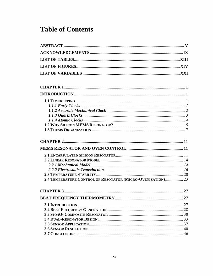
Table of Contents
ABSTRACT ................................................................................................................... V
ACKNOWLEDGEMENTS ......................................................................................... IX
LIST OF TABLES ..................................................................................................... XIII
LIST OF FIGURES ................................................................................................... XIV
LIST OF VARIABLES ............................................................................................. XXI
CHAPTER 1 .................................................................................................................... 1
INTRODUCTION .......................................................................................................... 1 1.1 TIMEKEEPING ......................................................................................................... 1
1.1.1 Early Clocks .................................................................................................... 1 1.1.2 Accurate Mechanical Clock ........................................................................... 2 1.1.3 Quartz Clocks .................................................................................................. 3 1.1.4 Atomic Clocks ................................................................................................. 4
1.2 WHY SILICON MEMS RESONATOR? .................................................................... 5 1.3 THESIS ORGANIZATION ......................................................................................... 7
CHAPTER 2 .................................................................................................................. 11
MEMS RESONATOR AND OVEN CONTROL ...................................................... 11 2.1 ENCAPSULATED SILICON RESONATOR ................................................................ 11 2.2 LINEAR RESONATOR MODEL .............................................................................. 14
2.2.1 Mechanical Model ........................................................................................ 14 2.2.2 Electrostatic Transduction ........................................................................... 16
2.3 TEMPERATURE STABILITY ................................................................................... 20 2.4 TEMPERATURE CONTROL OF RESONATOR (MICRO-OVENIZATION) ................. 23
CHAPTER 3 .................................................................................................................. 27
BEAT FREQUENCY THERMOMETRY ................................................................. 27 3.1 INTRODUCTION ..................................................................................................... 27 3.2 BEAT FREQUENCY GENERATION ......................................................................... 28 3.3 SI-SIO2 COMPOSITE RESONATOR ....................................................................... 30 3.4 DUAL-RESONATOR DESIGN ................................................................................. 33 3.5 SENSOR APPLICATION .......................................................................................... 37 3.6 SENSOR RESOLUTION ........................................................................................... 40 3.7 CONCLUSIONS ...................................................................................................... 46
xii
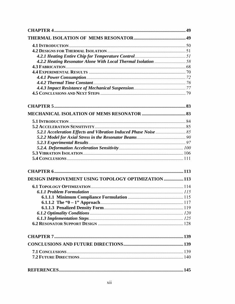
CHAPTER 4 .................................................................................................................. 49
THERMAL ISOLATION OF MEMS RESONATOR ............................................. 49 4.1 INTRODUCTION ..................................................................................................... 50 4.2 DESIGNS FOR THERMAL ISOLATION .................................................................... 51
4.2.1 Heating Entire Chip for Temperature Control ............................................ 51 4.2.2 Heating Resonator Alone With Local Thermal Isolation ........................... 58
4.3 FABRICATION ........................................................................................................ 68 4.4 EXPERIMENTAL RESULTS .................................................................................... 70
4.4.1 Power Consumption ...................................................................................... 72 4.4.2 Thermal Time Constant ................................................................................ 76 4.4.3 Impact Resistance of Mechanical Suspension ............................................. 77
4.5 CONCLUSIONS AND NEXT STEPS .......................................................................... 79
CHAPTER 5 .................................................................................................................. 83
MECHANICAL ISOLATION OF MEMS RESONATOR ...................................... 83 5.1 INTRODUCTION ..................................................................................................... 84 5.2 ACCELERATION SENSITIVITY ............................................................................... 85
5.2.1 Acceleration Effects and Vibration Induced Phase Noise .......................... 85 5.2.2 Model for Axial Stress in the Resonator Beams .......................................... 90 5.2.3 Experimental Results .................................................................................... 97 5.2.4. Deformation Acceleration Sensitivity ........................................................ 100
5.3 VIBRATION ISOLATION ....................................................................................... 106 5.4 CONCLUSIONS ..................................................................................................... 111
CHAPTER 6 ................................................................................................................ 113
DESIGN IMPROVEMENT USING TOPOLOGY OPTIMIZATION ................. 113 6.1 TOPOLOGY OPTIMIZATION ................................................................................ 114
6.1.1 Problem Formulation ................................................................................. 115 6.1.1.1 Minimum Compliance Formulation ................................................ 115 6.1.1.2 The “0 – 1” Approach ........................................................................ 117 6.1.1.3 Penalized Density Form ..................................................................... 119
6.1.2 Optimality Conditions ................................................................................. 120 6.1.3 Implementation Steps .................................................................................. 125
6.2 RESONATOR SUPPORT DESIGN .......................................................................... 128
CHAPTER 7 ................................................................................................................ 139
CONCLUSIONS AND FUTURE DIRECTIONS .................................................... 139 7.1 CONCLUSIONS ..................................................................................................... 139 7.2 FUTURE DIRECTIONS .......................................................................................... 140
REFERENCES ............................................................................................................ 145
xiii
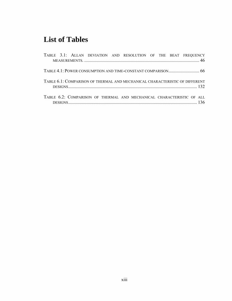
List of Tables
TABLE 3.1: ALLAN DEVIATION AND RESOLUTION OF THE BEAT FREQUENCY MEASUREMENTS. ..................................................................................................... 46
TABLE 4.1: POWER CONSUMPTION AND TIME-CONSTANT COMPARISON ........................... 66 TABLE 6.1: COMPARISON OF THERMAL AND MECHANICAL CHARACTERISTIC OF DIFFERENT
DESIGNS ................................................................................................................. 132 TABLE 6.2: COMPARISON OF THERMAL AND MECHANICAL CHARACTERISTIC OF ALL
DESIGNS ................................................................................................................. 136
xiv
List of Figures
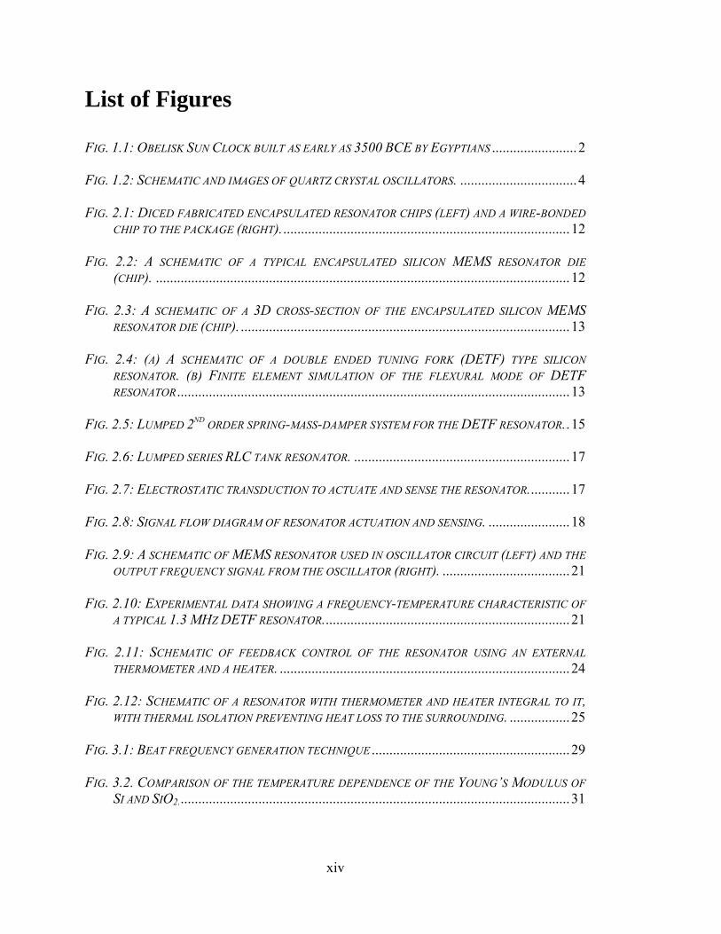
FIG. 1.1: OBELISK SUN CLOCK BUILT AS EARLY AS 3500 BCE BY EGYPTIANS ........................ 2 FIG. 1.2: SCHEMATIC AND IMAGES OF QUARTZ CRYSTAL OSCILLATORS. ................................. 4 FIG. 2.1: DICED FABRICATED ENCAPSULATED RESONATOR CHIPS (LEFT) AND A WIRE-BONDED
CHIP TO THE PACKAGE (RIGHT). ................................................................................. 12 FIG. 2.2: A SCHEMATIC OF A TYPICAL ENCAPSULATED SILICON MEMS RESONATOR DIE
(CHIP). ..................................................................................................................... 12 FIG. 2.3: A SCHEMATIC OF A 3D CROSS-SECTION OF THE ENCAPSULATED SILICON MEMS
RESONATOR DIE (CHIP). ............................................................................................. 13 FIG. 2.4: (A) A SCHEMATIC OF A DOUBLE ENDED TUNING FORK (DETF) TYPE SILICON
RESONATOR. (B) FINITE ELEMENT SIMULATION OF THE FLEXURAL MODE OF DETF RESONATOR ............................................................................................................... 13
FIG. 2.5: LUMPED 2ND ORDER SPRING-MASS-DAMPER SYSTEM FOR THE DETF RESONATOR. . 15 FIG. 2.6: LUMPED SERIES RLC TANK RESONATOR. ............................................................. 17 FIG. 2.7: ELECTROSTATIC TRANSDUCTION TO ACTUATE AND SENSE THE RESONATOR. ........... 17 FIG. 2.8: SIGNAL FLOW DIAGRAM OF RESONATOR ACTUATION AND SENSING. ....................... 18 FIG. 2.9: A SCHEMATIC OF MEMS RESONATOR USED IN OSCILLATOR CIRCUIT (LEFT) AND THE
OUTPUT FREQUENCY SIGNAL FROM THE OSCILLATOR (RIGHT). .................................... 21 FIG. 2.10: EXPERIMENTAL DATA SHOWING A FREQUENCY-TEMPERATURE CHARACTERISTIC OF
A TYPICAL 1.3 MHZ DETF RESONATOR. ..................................................................... 21 FIG. 2.11: SCHEMATIC OF FEEDBACK CONTROL OF THE RESONATOR USING AN EXTERNAL
THERMOMETER AND A HEATER. .................................................................................. 24 FIG. 2.12: SCHEMATIC OF A RESONATOR WITH THERMOMETER AND HEATER INTEGRAL TO IT,
WITH THERMAL ISOLATION PREVENTING HEAT LOSS TO THE SURROUNDING. ................. 25 FIG. 3.1: BEAT FREQUENCY GENERATION TECHNIQUE ........................................................ 29 FIG. 3.2. COMPARISON OF THE TEMPERATURE DEPENDENCE OF THE YOUNG’S MODULUS OF
SI AND SIO2. .............................................................................................................. 31
xv
FIG. 3.3. (A) SEM IMAGE OF A COMPOSITE SILICON RESONATOR BEAM WITH THE THERMALLY GROWN SIO2 LAYER. (B) ENLARGED VIEW. ................................................................. 32
FIG. 3.4. EXPERIMENTAL DATA SHOWING THE COMPARISON OF TCF OF BARE SILICON AND
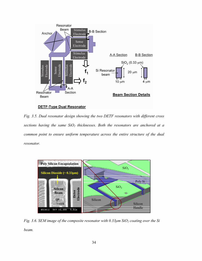
THE COMPOSITE SILICON. .......................................................................................... 32 FIG. 3.5. DUAL RESONATOR DESIGN SHOWING THE TWO DETF RESONATORS WITH DIFFERENT
CROSS SECTIONS HAVING THE SAME SIO2 THICKNESSES. BOTH THE RESONATORS ARE ANCHORED AT A COMMON POINT TO ENSURE UNIFORM TEMPERATURE ACROSS THE ENTIRE STRUCTURE OF THE DUAL RESONATOR. ........................................................... 34
FIG. 3.6. SEM IMAGE OF THE COMPOSITE RESONATOR WITH 0.33ΜM SIO2 COATING OVER THE
SI BEAM. ................................................................................................................... 34 FIG. 3.7. EXPERIMENTAL DATA SHOWING TEMPERATURE DEPENDENCE OF F1 AND F2 OF THE
DUAL RESONATOR. .................................................................................................... 35 FIG. 3.8. ILLUSTRATION OF THE BEAT FREQUENCY GENERATION TECHNIQUE USING DUAL
RESONATOR. ............................................................................................................. 36 FIG. 3.9: EXPERIMENTAL DATA SHOWING COMPARISON OF THE TEMPERATURE DEPENDENCE
OF THE BEAT FREQUENCY WITH THAT OF THE DUAL RESONATOR FREQUENCIES. .......... 38 FIG. 3.10: EXPERIMENTAL DATA SHOWING TEMPERATURE DEPENDENCE OF FBEAT FOR
VARIOUS DESIGNS HAVING RESONATOR FREQUENCIES IN THE RANGE OF 1.0MHZ, 1.5MHZ AND 2.5MHZ. ............................................................................................. 38
FIG. 3.11: EXPERIMENTAL DATA SHOWING RESONATOR F-T CHARACTERISTIC IN RAPID-
TEMPERATURE CYCLING (SLEW RATE ~ 6°C /MIN) USING (A) AN EXTERNAL TEMPERATURE SENSOR – PT. RTD (B) BEAT FREQUENCY AS A TEMPERATURE SENSOR. ........................ 39
FIG. 3.12: BLOCK DIAGRAM SHOWING THE MODELING OF CORRELATION TECHNIQUE. ........ 41 FIG. 3.13: MEASUREMENT OF THE BEAT FREQUENCIES OF THE TWO DIFFERENT DUAL-
RESONATOR DEVICES AT A NOMINALLY CONSTANT TEMPERATURE. BOTH DEVICES WERE KEPT INSIDE AN OVEN SIDE-SIDE AND THE OVEN WAS MAINTAINED AT A NOMINALLY CONSTANT TEMPERATURE OF 60°C. ........................................................................... 44
FIG. 3.14: EVALUATION OF THE ALLAN DEVIATION OF THE MEASURED BEAT FREQUENCY DATA
AND ITS NOISE. .......................................................................................................... 45 FIG. 4.1: SCHEMATIC OF A TYPICAL MEMS RESONATOR CHIP ATTACHED TO A PACKAGE WITH
ADHESIVE. ................................................................................................................ 52
xvi
FIG. 4.2: (A) TOP VIEW SCHEMATIC OF A STANDARD UN-ISOLATED DETF-TYPE RESONANT STRUCTURE SHOWING INPUT AND OUTPUT ELECTRODES. (B) FEM SIMULATION OF FLEXURAL- VIBRATION MODE OF A DETF (EXAGGERATED VIEW). ............................... 53
FIG. 4.3: THERMAL EQUIVALENT CIRCUIT. PACKAGE IS ASSUMED TO BE AT AMBIENT
TEMPERATURE. UNIT OF THERMAL RESISTANCES SHOWN ABOVE IN KELVIN PER WATT. . 55 FIG. 4.4: FLOATING CHIP WITHOUT ANY ADHESIVE AT THE BOTTOM TO INCREASE THE
THERMAL RESISTANCE. ............................................................................................... 56 FIG. 4.5: THERMAL EQUIVALENT CIRCUIT WHEN THERE IS RADIATIVE HEAT LOSS FROM THE
BOTTOM OF THE CHIP RRADBOT IN THE ABSENCE OF THE ADHESIVE. UNIT OF THERMAL RESISTANCES SHOWN ABOVE IS IN KELVIN PER WATT. .................................................. 57
FIG. 4.6: (A) TEMPERATURE PROFILE ALONG THE LENGTH OF A CURRENT-CARRYING
RESISTIVE HEATER HAVING THERMAL RESISTANCE OF RTH AND ELECTRICAL RESISTANCE OF RE. (B) THE CONTINUOUS TEMPERATURE PROFILE AND ITS APPROXIMATE EQUIVALENT LUMPED MODEL. ................................................................................... 61
FIG. 4.7: RESONATOR DESIGN WITH LOCAL THERMAL ISOLATION. THE HEATER IS IN-BUILT TO
THE DETF SUCH THAT THE RESONANT STRUCTURE IS ATTACHED AT THE CENTER OF THE HEATER. THE ENTIRE STRUCTURE IS RELEASED EXCEPT AT THE FOUR ANCHORS. .......... 62
FIG. 4.8: ONE DIMENSIONAL RESISTOR NETWORK TO ESTIMATE THE TOTAL EFFECTIVE
THERMAL RESISTANCE OF THE IN-BUILT HEATER. EQUATION (4.10) IS USED FOR THE ESTIMATION OF EFFECTIVE THERMAL RESISTANCE REFF. .............................................. 63
FIG. 4.9: EQUIVALENT THERMAL CIRCUIT SCHEMATIC FOR THE RESONATOR WITH IN-BUILT
HEATER. .................................................................................................................... 67 FIG. 4.10: FINITE-ELEMENT SIMULATION OF THE THERMALLY ISOLATED DETF RESONATOR
SHOWING THE TEMPERATURE DISTRIBUTION IN KELVIN FOR A HEATING VOLTAGE OF 6 V, WHICH CORRESPONDS TO 14 MW OF HEATING POWER. ............................................... 67
FIG. 4.11: (A) OPTICAL IMAGE OF THE TOP VIEW OF THE FABRICATED DEVICE BEFORE THE
DEPOSITION OF THE ENCAPSULATION LAYER. (B) SEM CROSS SECTION OF A RESONATOR BEAM AFTER THE DEPOSITION OF THE ENCAPSULATION LAYER. ................................... 69
FIG. 4.12: ISOMETRIC VIEW OF DEVICE LAYER SCHEMATIC SHOWING THE DETF WITH THE IN-
BUILT HEATER. A STIMULUS SIGNAL IS APPLIED TO THE INPUT ELECTRODE. HEATING VOLTAGES V1 AND V2 ARE CONTROLLED USING A FEEDBACK CONTROL LOOP TO MAINTAIN A CONSTANT BIAS FOR THE RESONATOR. ...................................................... 71
FIG. 4.13: SCHEMATIC OF THE TEST SETUP FOR FREQUENCY MEASUREMENT. ...................... 71 FIG. 4.14: EXPERIMENTAL DATA SHOWING VARIATION OF RESONATOR FREQUENCY DUE TO
JOULE HEATING OF THE IN-BUILT HEATER. THE DECREASE IN FREQUENCY (RIGHT Y-AXIS)
xvii
CORRESPONDS TO A TEMPERATURE RISE (LEFT Y-AXIS) WITH INCREASING INPUT POWER. EXPERIMENTAL RESULTS ARE COMPARED WITH THEORETICAL ESTIMATES. THE ANALYTICAL EXPRESSION (10) ESTIMATES THE TEMPERATURE AT THE CENTER OF THE IN-BUILT HEATER, WHILE THE FEM RESULTS ARE FOR THE TEMPERATURE AT THE CENTER OF THE RESONATOR. .................................................................................................. 73
FIG. 4.15: EXPERIMENTAL DATA SHOWING FREQUENCY – TEMPERATURE CHARACTERIZATION
OF THE RESONATOR WITH IN-BUILT HEATER. THE RESONATOR WAS KEPT INSIDE AN OVEN AND THE OVEN TEMPERATURE WAS VARIED TO FIND OUT THE TCF OF THE RESONATOR UNDER NO JOULE HEATING. THE TCF OF THIS RESONATOR CORRESPONDS TO THAT OF A STRESS FREE SINGLE ANCHORED RESONATOR. ............................................................ 74
FIG. 4.16: DYNAMIC THERMAL RESPONSE OF THE MICRO-OVENIZED RESONATOR. (INSET) THE
IN-BUILT HEATER FORMED ONE LEG OF A WHEATSTONE BRIDGE. THE MEASURED VOLTAGE OUTPUT FROM THE BRIDGE REPRESENTS THE CHANGE IN HEATER RESISTANCE AS THE HEATER COOLS DOWN FOLLOWING A HEATING PULSE. ..................................... 77
FIG. 4.17: DROP TEST RESULTED IN A TEMPORARY CHANGE IN FREQUENCY AT THE TIME OF
DROP. ....................................................................................................................... 78 FIG. 4.18: COMPARATIVE REGIME MAP SHOWING THE POWER CONSUMPTION AND THERMAL
TIME CONSTANT OF IN-BUILT HEATER RESONATOR, STANDARD RESONATOR AND QUARTZ OCXO. .................................................................................................................... 79
FIG. 5.1: A TYPICAL PLOT SHOWING THE EFFECT OF ACCELERATION IN X-DIRECTION ON THE
CHANGE IN RESONATOR FREQUENCY. THE SLOPE OF THE CURVE IS ACCELERATION SENSITIVITY IN X-DIRECTION ( .............................................................................. 85
FIG. 5.2: INSTANTANEOUS CARRIER FREQUENCY FOR SEVERAL INSTANTS DURING ONE CYCLE
OF VIBRATION. .......................................................................................................... 87 FIG. 5.3: TIME DEPENDENT ACCELERATION (TOP) AND RESULTING OSCILLATOR OUTPUT
SHOWING FREQUENCY MODULATION (BOTTOM). ........................................................ 87 FIG. 5.4: VIBRATION INDUCED SIDEBANDS AND CARRIER RESULTING FROM SINUSOIDAL
ACCELERATION AT FREQUENCY . ........................................................................... 89 FIG. 5.5: (A) THE SCHEMATIC OF THE BASIC SINGLE ANCHORED DETF RESONATOR. THE
EFFECT OF THE EXTERNAL ACCELERATION AX IS MODELED BY A SPRING MASS SYSTEM, WHERE M IS THE COUPLING MASS, K IS THE STIFFNESS OF THE RESONATOR BEAM AND U IS THE DISPLACEMENT DUE TO INERTIA FORCE GENERATED BY THE EXTERNAL ACCELERATION AX. (B) THE SCHEMATIC OF A SPRING SUPPORTED DETF RESONATOR SHOWING SERPENTINE TYPE RESISTIVE SILICON SUSPENSION ON BOTH SIDES OF THE RESONATOR WITH STIFFNESS K1 AND K3. THE STIFFNESS OF THE RESONATOR BEAM, IN THIS CASE, IS REPRESENTED BY K2. ............................................................................. 92
xviii
FIG. 5.6: FINITE ELEMENT SIMULATION OF THE STANDARD RESONATOR (TOP) AND THE SPRING MOUNTED RESONATOR (BOTTOM) FOR ACCELERATION IN THE X DIRECTION AX. THE RESULT SHOWS THE DEFORMATION OF THE RESONATOR DUE TO THE BODY LOAD GENERATED BY THE ACCELERATION. THE DEFORMATION SHOWN ABOVE IS EXAGGERATED. ......................................................................................................... 95
FIG. 5.7: FINITE ELEMENT SIMULATION SHOWING THE CHANGE IN FREQUENCY WITH RESPECT
TO THE ACCELERATION FOR BASIC RESONATOR AS WELL AS FOR SPRING SUPPORTED RESONATOR. .............................................................................................................. 96
FIG. 5.8: SCHEMATIC OF DYNAMIC VIBRATION EXPERIMENTAL SETUP. THE RESONATOR
DEVICE ATTACHED IN A PACKAGE IS SOLDERED INTO THE PCB WHICH IN TURN IS MOUNTED ON THE SHAKER. THE SHAKER IS ACTUATED USING A FREQUENCY GENERATOR AND THE AMPLITUDE OF THE SHAKER VIBRATION IS MEASURED BY LASER VIBROMETER. THE OSCILLATOR OUTPUT IS MEASURED USING A SPECTRUM ANALYZER. ...................... 97
FIG. 5.9: EXPERIMENTAL RESULT SHOWING THE EFFECT OF VIBRATION ON A BASIC SINGLE
ANCHORED DETF RESONATOR. THE SINUSOIDAL VIBRATION WAS APPLIED IN X-DIRECTION AT 150 HZ WITH 30G ACCELERATION. THE PRESENCE OF EXTERNAL VIBRATION CAUSES SIDEBANDS AT 150 HZ. ................................................................. 98
FIG. 5.10: EXPERIMENTAL RESULT SHOWING THE EFFECT OF VIBRATION ON A SPRING
SUPPORTED DETF RESONATOR. THE SINUSOIDAL VIBRATION WAS APPLIED IN X-DIRECTION AT 150 HZ WITH 30G ACCELERATION. THE PRESENCE OF EXTERNAL VIBRATION CAUSES NO VISIBLE SIDEBANDS. IN OTHER WORDS, THE SIDEBANDS ARE BURIED IN THE NOISE. ................................................................................................ 99
FIG. 5.11: A TYPICAL PLOT SHOWING THE EFFECT OF ACCELERATION IN A PARTICULAR
DIRECTION ON THE DEFORMATION OF THE RESONATOR BEAM. THE SLOPE OF THE CURVE IS ACCELERATION SENSITIVITY IN THAT PARTICULAR DIRECTION. ................................ 100
FIG. 5.12: (A) SCHEMATIC SHOWING A SYMMETRIC GAP OF D BETWEEN THE RESONATOR BEAM
AND THE ELECTRODES. (B) THE RESONATOR BEAM IS SHIFTED TOWARDS ONE ELECTRODE BY X DUE TO EXTERNAL FORCE. FOR SIMPLICITY, IT IS ASSUMED THAT THE BEAM SHIFT IS UNIFORM ACROSS ITS LENGTH. ................................................................................. 105
FIG. 5.13: VIBRATION ISOLATION FREQUENCY RESPONSE. ................................................ 107 FIG. 5.14: MODELING OF THE STRUCTURE DYNAMICS OF THE DETF RESONATOR (TOP).
SPRING MASS MODEL OF THE RESONATOR (BOTTOM). ............................................... 109 FIG. 6.1: STRUCTURAL OPTIMIZATION CATEGORIZED INTO SIZE, SHAPE AND TOPOLOGY
OPTIMIZATION. (COURTESY: DR. I. Y. KIM) .............................................................. 114 FIG. 6.2: FLOW CHART FOR THE IMPLEMENTATION OF THE TOPOLOGY OPTIMIZATION. ...... 125
xix
FIG. 6.3: THE STARTING DOMAIN (TOP) WHICH IS BASED ON A CLEVER GUESS ON THE ASSUMPTION THAT THE FINAL SHAPE IS ENCLOSED IN IT. THE CHANGE IN THE DISTRIBUTION OF THE BLACK-WHITE PATTERN IS SHOWN (BOTTOM) AFTER ITERATION NUMBER 1, 10 AND 56 LEADING TO THE FINAL SHAPE. .............................................. 127
FIG. 6.4: MODELING OF THE EXTERNAL IMPACT FORCES AND THE RESULTING REACTION
FORCES AT THE SUPPORT ANCHORS. ......................................................................... 129 FIG. 6.5: (A) STARTING DOMAIN FOR THE RESONATOR SUPPORT STRUCTURE ASSUMING THAT
THE FINAL SHAPE OF THE STRUCTURE WILL LIE WITHIN THIS DOMAIN. (B) FINAL SHAPE OBTAINED USING THE TOPOLOGY OPTIMIZATION ALGORITHM. (C) ANALYTICALLY PROVEN SHAPE OF 2-BAR FRAME WITH 90° ANGLE FOR OPTIMAL STIFFNESS. .......................... 130
FIG. 6.6: RESONATOR WITH 2-BAR ISOLATING TETHER WHICH ACTS AS ANCHOR SUPPORT WITH
90° ANGLE BETWEEN THEM. .................................................................................... 130 FIG. 6.7: RESONATOR WITH 2-BAR ISOLATING TETHER HAVING MICRO-SERPENTINE
STRUCTURE FOR INCREASED THERMAL RESISTANCE OF APPROXIMATELY 300,000 K/W. (THE ANCHORS ARE NOT SHOWN IN THE ABOVE FIGURE FOR BETTER CLARITY). .......... 131
FIG. 6.8: FINITE ELEMENT SIMULATION OF THE RESONATOR WITH IMPROVED THERMAL
ISOLATION DESIGN SHOWING TEMPERATURE GRADIENT ACROSS THE LENGTH OF THE RESONATOR BEAM. THE TEMPERATURE GRADIENT IS PROPORTIONAL TO THE THERMAL RESISTANCE OF THE BEAM AND THE APPLIED HEATING VOLTAGE ACROSS THE ANCHORS. .............................................................................................................................. 133
FIG. 6.9: A SCHEMATIC OF THE FORCE BALANCE IN THE SINGLE-ANCHORED RESONATOR DUE
TO EXTERNAL IMPACT. A COUPLE, AT THE ANCHOR, IS REQUIRED TO COUNTER BALANCE THE IMPACT. ........................................................................................................... 134
FIG. 6.10: RESONATOR WITH SINGLE-SIDE ANCHORS WITH TETHERS HAVING MICRO-
SERPENTINE STRUCTURE FOR INCREASED THERMAL RESISTANCE OF APPROXIMATELY 300,000 K/W. (THE ANCHORS ARE NOT SHOWN IN THE ABOVE FIGURE FOR BETTER CLARITY). ............................................................................................................... 135
FIG. 6.11: FINITE ELEMENT SIMULATION OF THE SINGLE-SIDED ANCHOR RESONATOR DESIGN
SHOWING UNIFORM TEMPERATURE ACROSS THE LENGTH OF THE RESONATOR BEAM. .. 136 FIG. 7.1: VIBRATION MEASUREMENT OF A RUNNING (ENGINE TURNED ON) CAR BY ATTACHING
ACCELEROMETERS AT VARIOUS LOCATIONS. ............................................................. 140 FIG. 7.2: VIBRATION SPECTRUM OUTPUT WHEN THE ENGINE WAS IDLING AND THE
ACCELEROMETERS WERE ATTACHED AT THE ENGINE COVER. ..................................... 141 FIG. 7.3: VIBRATION SPECTRUM OUTPUT AT DIFFERENT ENGINE SPEEDS (RPM). ............... 141
xx
FIG. 7.4: FEM SIMULATION SHOWING STRESS CONCENTRATION ON THE DESIGNS NORMALLY USED FOR ENERGY SCAVENGING. .............................................................................. 142
xxi
List of Variables
k Thermal conductivity, W m−1 K−1.
ε Surface emissivity, 0 ≤ ε ≤ 1.
σ Stefan–Boltzmann constant,5.67×10−8Wm−2K−4.
ρ Density, kg m−3.
Cp Specific heat capacity at constant pressure, J kg−1 K−1.
Re Electrical resistance, Ω.
Rth Thermal resistance, K W−1.
C Specific heat per unit volume at constant volume, J m−3 K−1.
ν Velocity of the energy carrier, m s−1.
KB Boltzmann constant, 1.381 × 10⁻²³ J K−1.
nm Molecular number density, m−3.
m Molecular mass of the energy carrier, or lumped mass kg.
T Temperature, K.
V’ Volume, m3.
V Voltage, V.
Cchip Thermal capacitance of chip, J K−1.
Cresonator Thermal capacitance of resonator, J K−1.
Ac Cross-sectional area, m2.
As Surface area, m2.
q’ Rate of joule heat per unit volume, W m−3.
q Rate of total heat generated, W.
l Length, m.
xxii
E Modulus of elasticity, N m−2.
I Area moment of inertia, m4.
P Axial force, N.
ml Mass per unit length, kg m−1.
fr, Frequency, Hz.
b Damping coefficient, N.s. m−1
k, k1, k2, k3 Stiffness, N m−1 Q Quality factor
Natural frequency, rad s-1
Electrical bias voltage
Input ac stimulus voltage
, Capacitance for input and output electrodes with the resonator beam
Output electric current
, Electrostatic transduction factor
d, g Gap between the electrodes and the resonator beam, m
Motional resistance, Ω
Mode constant
Cross correlation coefficient between two measurements y1 and y2 Γ Acceleration sensitivity in x direction, ppm g-1
Acceleration in x direction, g
Resonator frequency without acceleration, or carrier frequency, Hz
Frequency of external vibration, Hz t Time, s
xxiii
u, u1, u2 Displacement, m
Linearized strain K Global stiffness matrix Ke Element stiffness matrix
Young’s modulus of a discrete element (used for stiffness matrix)
Density function f, fext Force, N Λ, , Lagrange multiplier p Penalty function c Compliance

xxiv
1
Chapter 1 Introduction
1.1 Timekeeping
A resonator is used to create an oscillator which can be used for frequency reference or
timekeeping. People have been making a constant effort to measure time as accurately
as possible since several thousand years ago. Around 3100 BCE (Before the Common
Era) Egyptians devised a 365 day calendar which seems to be one of the earliest years
recorded in history [1] – [3].
1.1.1 Early Clocks
All clocks must have two basic components: a repetitive process or action which occurs
at a regular interval of time, and a means of measuring or keeping track of the time
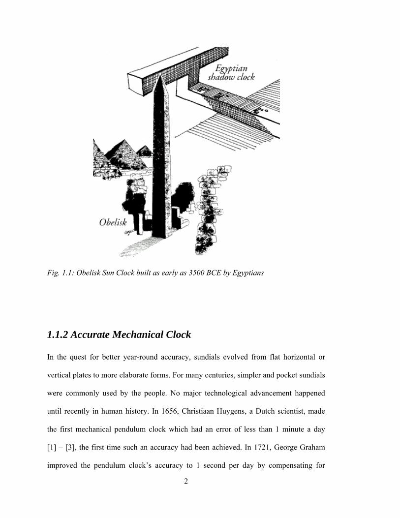
interval. Sun Clocks in the form of Obelisks, Fig. 1.1, were built by Egyptians around
3500 BCE [1] – [3]. The moving shadows of Obelisk (slender, tapering, four-sided
monument) formed a kind of sundial enabling people to partition the day into morning
and afternoon. Water clocks were among the earliest timekeepers which didn’t rely on
celestial bodies. Greeks began using them around 325 BCE to determine hours at night
[1] – [3]. These were stone vessels that allowed dripping water at a nearly constant rate
from a small hole near the bottom.
2
Fig. 1.1: Obelisk Sun Clock built as early as 3500 BCE by Egyptians
1.1.2 Accurate Mechanical Clock
In the quest for better year-round accuracy, sundials evolved from flat horizontal or
vertical plates to more elaborate forms. For many centuries, simpler and pocket sundials
were commonly used by the people. No major technological advancement happened
until recently in human history. In 1656, Christiaan Huygens, a Dutch scientist, made
the first mechanical pendulum clock which had an error of less than 1 minute a day
[1] – [3], the first time such an accuracy had been achieved. In 1721, George Graham
improved the pendulum clock’s accuracy to 1 second per day by compensating for
3
changes in the pendulum’s length due to temperature variations. Over the next centuries
further refinements led to more and more accurate clocks.
1.1.3 Quartz Clocks
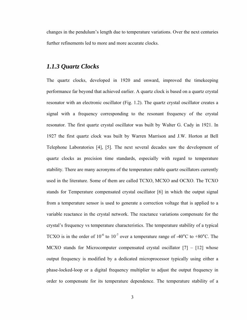
The quartz clocks, developed in 1920 and onward, improved the timekeeping
performance far beyond that achieved earlier. A quartz clock is based on a quartz crystal
resonator with an electronic oscillator (Fig. 1.2). The quartz crystal oscillator creates a
signal with a frequency corresponding to the resonant frequency of the crystal
resonator. The first quartz crystal oscillator was built by Walter G. Cady in 1921. In
1927 the first quartz clock was built by Warren Marrison and J.W. Horton at Bell
Telephone Laboratories [4], [5]. The next several decades saw the development of
quartz clocks as precision time standards, especially with regard to temperature
stability. There are many acronyms of the temperature stable quartz oscillators currently
used in the literature. Some of them are called TCXO, MCXO and OCXO. The TCXO
stands for Temperature compensated crystal oscillator [6] in which the output signal
from a temperature sensor is used to generate a correction voltage that is applied to a
variable reactance in the crystal network. The reactance variations compensate for the
crystal’s frequency vs temperature characteristics. The temperature stability of a typical
TCXO is in the order of 10-6 to 10-7 over a temperature range of -40°C to +80°C. The
MCXO stands for Microcomputer compensated crystal oscillator [7] – [12] whose
output frequency is modified by a dedicated microprocessor typically using either a
phase-locked-loop or a digital frequency multiplier to adjust the output frequency in
order to compensate for its temperature dependence. The temperature stability of a
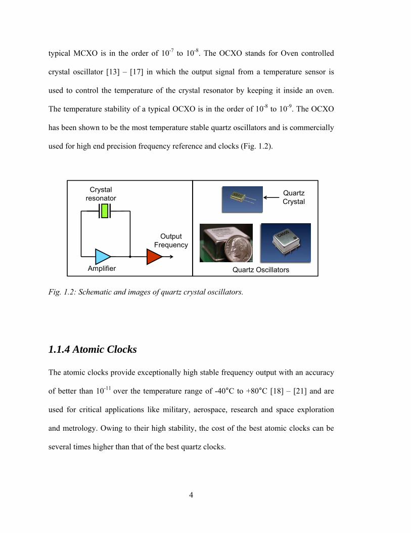
4
typical MCXO is in the order of 10-7 to 10-8. The OCXO stands for Oven controlled
crystal oscillator [13] – [17] in which the output signal from a temperature sensor is
used to control the temperature of the crystal resonator by keeping it inside an oven.
The temperature stability of a typical OCXO is in the order of 10-8 to 10-9. The OCXO
has been shown to be the most temperature stable quartz oscillators and is commercially
used for high end precision frequency reference and clocks (Fig. 1.2).
Fig. 1.2: Schematic and images of quartz crystal oscillators.
1.1.4 Atomic Clocks
The atomic clocks provide exceptionally high stable frequency output with an accuracy
of better than 10-11 over the temperature range of -40°C to +80°C [18] – [21] and are
used for critical applications like military, aerospace, research and space exploration
and metrology. Owing to their high stability, the cost of the best atomic clocks can be
several times higher than that of the best quartz clocks.
Crystalresonator
Amplifier
OutputFrequency
QuartzCrystal
Quartz Oscillators
5
The principle of operation of the atomic clock is based on the energy state of the atom.
When an atom changes energy from an excited state to a lower energy state, a photon is
emitted. The photon frequency ν is given by Planck’s law
1.1
where E2 and E1 are the energies of the upper and lower states, respectively, and h is
Planck’s constant. The atomic clock is based on the above principle where the
frequency is determined by the intrinsic properties of an atom. There are various types
of atomic clocks. For detail understanding of atomic clocks and frequency standards,
refer to [18] – [21].
1.2 Why Silicon MEMS Resonator?
MEMS stands for “Micro Electro Mechanical System”. Silicon MEMS resonator has
the potential to replace quartz crystal for timing and frequency reference application
[22] – [30]. Beyond frequency references, MEMS resonators can also be used as a
sensor [31] – [42], RF filters and mixers [43] – [44], and atomic force microscopy [45].
Sensors for mass (vapor, chemicals, protein, etc.) [31] – [35], pressure [36], [37], strain,
force and acceleration [38] – [41], and temperature [42] are well reported in the
literature.
6
Almost all electronic instruments and communication system use some kind of timer or
frequency reference; and this multi-billion dollar oscillator market is currently
dominated by quartz crystal. Silicon micromechanical resonator has several advantages
over quartz resonator. Some of its advantages are related to its fabrication technology
which leverages the IC fabrication technology allowing it to be CMOS compatible [46],
[47], resulting into lower cost, smaller form factors, increased reliability and
manufacturability, and single chip solutions. Previous research work has shown that the
silicon micromechanical resonator has excellent long term stability of better than 1ppm
[48] – [50] and a temperature stability of upto 10-7 [51], [52]. However, there are some
challenges to overcome in terms of achieving temperature stability close to that of
OCXO (10-9).
One of the biggest advantages of MEMS resonator, not mentioned above, is its low
power consumption and a good dynamic thermal response. As mentioned before, oven
controlled oscillators provide better temperature stability due to feedback control of
resonator temperature. However, the temperature control or ovenization of the resonator
leads to power consumption. In case of quartz, that is OCXO, this power consumption
can be huge and can go up to several watts [13] – [17] compared to sub-watt power
consumption in MEMS resonator [53] – [56]. Another factor which is key to the
performance of oven controlled oscillators is its dynamic thermal response, where
MEMS resonator outweighs quartz crystal. The advantages of low power consumption
and a good dynamic thermal response of MEMS resonator are simply due to its small
size. It is possible to further reduce its power consumption and the dynamic thermal
7
response by better design and optimization. The thesis focuses on this aspect of the
research work. Also, for oven controlled oscillators a temperature sensor with low
thermal lag and high resolution is required. The OCXO uses a beat frequency based
temperature sensor which allows the quartz crystal resonator to sense its own
temperature thereby eliminating any thermal lag. One of the main reasons for OCXO to
achieve high temperature stability is the realization of the beat frequency thermometry.
This technique of temperature sensing was difficult to realize in MEMS resonator
before. The thesis also demonstrates on silicon resonator based beat frequency
thermometry.
1.3 Thesis Organization
The main contribution of this thesis is the silicon micromechanical resonator based beat
frequency thermometry, thermal isolation of the resonator to reduce the power
consumption for oven control oscillator, analysis of mechanical isolation of the
resonator to understand the mechanical stability of the device, and the topology
optimization of the resonator structure to increase both the thermal as well as the
mechanical isolation simultaneously. The rest of this thesis is organized as follows:
Chapter 2 describes the modeling of the electrostatic MEMS resonator and the
schematic of the micro-oven controlled oscillators, explaining the importance of a good
thermometer and the thermal isolation.
8
Chapter 3 presents a beat frequency digital temperature sensing technique using a
CMOS compatible encapsulated micromechanical resonator. A dual-resonator design is
described that includes a pair of resonators with differential temperature compensations
so that the difference between the two resonant frequencies is a sensitive function of
temperature. We demonstrate a temperature resolution of approximately 0.008 °C for 1
s averaging time, which is better than that of the best CMOS temperature sensors
available today.
Chapter 4 demonstrates an efficient local-thermal-isolation mechanism for a micro-oven
controlled resonator, which can reduce the power requirement by 20x and the thermal
time constant by 50x. In this method, the mechanical suspension of the resonator is
modified to provide thermal isolation and include an integrated resistive heater. This
combination provides mechanical suspension, electrical heating, and thermal isolation
in a compact structure that requires low heating power and has a small thermal time
constant.
Chapter 5 describes the analysis of the mechanical isolation of the silicon
micromechanical resonator. The chapter presents an investigative study of mechanical
robustness of the electrostatically coupled encapsulated DETF resonator. This study of
mechanical isolation of the resonator is necessary in order to understand the limit of the
thermal isolation.
9
Chapter 6 gives an analysis of topology optimization of the MEMS resonator structure
to improve both the thermal and mechanical isolation simultaneously. A new design
having 2x further reduction in power consumption and 10x improvement in the
mechanical stiffness is described.
Chapter 7 is a conclusive summary of the work and the possible future direction.

10
11
Chapter 2
MEMS Resonator and Oven Control
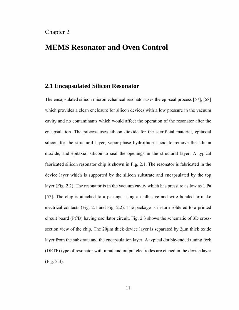
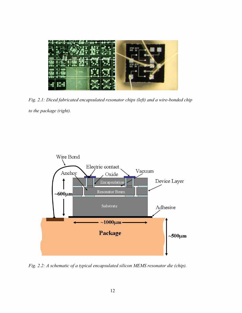
2.1 Encapsulated Silicon Resonator
The encapsulated silicon micromechanical resonator uses the epi-seal process [57], [58]
which provides a clean enclosure for silicon devices with a low pressure in the vacuum
cavity and no contaminants which would affect the operation of the resonator after the
encapsulation. The process uses silicon dioxide for the sacrificial material, epitaxial
silicon for the structural layer, vapor-phase hydrofluoric acid to remove the silicon
dioxide, and epitaxial silicon to seal the openings in the structural layer. A typical
fabricated silicon resonator chip is shown in Fig. 2.1. The resonator is fabricated in the
device layer which is supported by the silicon substrate and encapsulated by the top
layer (Fig. 2.2). The resonator is in the vacuum cavity which has pressure as low as 1 Pa
[57]. The chip is attached to a package using an adhesive and wire bonded to make
electrical contacts (Fig. 2.1 and Fig. 2.2). The package is in-turn soldered to a printed
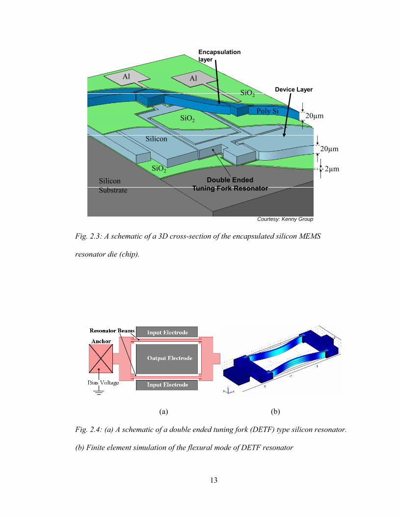
circuit board (PCB) having oscillator circuit. Fig. 2.3 shows the schematic of 3D cross-
section view of the chip. The 20μm thick device layer is separated by 2μm thick oxide
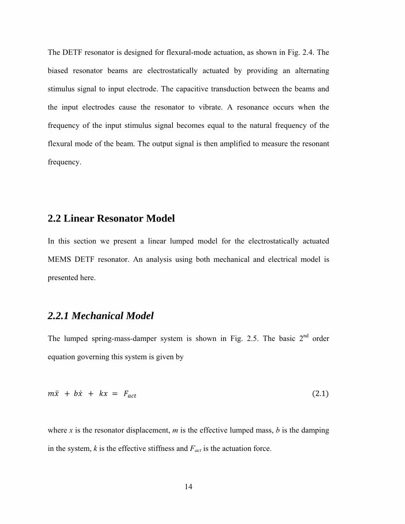
layer from the substrate and the encapsulation layer. A typical double-ended tuning fork
(DETF) type of resonator with input and output electrodes are etched in the device layer
(Fig. 2.3).
12
Fig. 2.1: Diced fabricated encapsulated resonator chips (left) and a wire-bonded chip
to the package (right).
Fig. 2.2: A schematic of a typical encapsulated silicon MEMS resonator die (chip).
13
Fig. 2.3: A schematic of a 3D cross-section of the encapsulated silicon MEMS
resonator die (chip).
(a) (b)
Fig. 2.4: (a) A schematic of a double ended tuning fork (DETF) type silicon resonator.
(b) Finite element simulation of the flexural mode of DETF resonator
SiliconSubstrate
SiO2
SiO2
SiO2
Silicon
AlAl
Poly Si
20µm
20µm
2µmDouble Ended
Tuning Fork Resonator
Device Layer
Encapsulationlayer
Courtesy: Kenny Group
14
The DETF resonator is designed for flexural-mode actuation, as shown in Fig. 2.4. The
biased resonator beams are electrostatically actuated by providing an alternating
stimulus signal to input electrode. The capacitive transduction between the beams and
the input electrodes cause the resonator to vibrate. A resonance occurs when the
frequency of the input stimulus signal becomes equal to the natural frequency of the
flexural mode of the beam. The output signal is then amplified to measure the resonant
frequency.
2.2 Linear Resonator Model
In this section we present a linear lumped model for the electrostatically actuated
MEMS DETF resonator. An analysis using both mechanical and electrical model is
presented here.
2.2.1 Mechanical Model
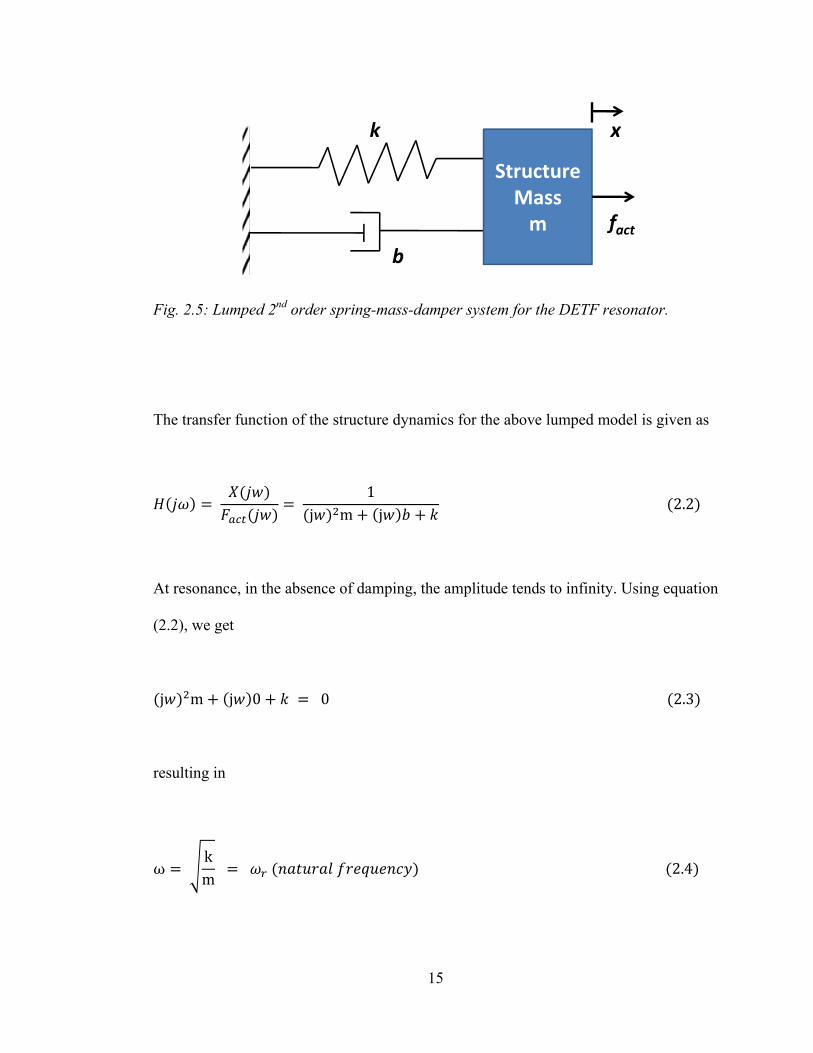
The lumped spring-mass-damper system is shown in Fig. 2.5. The basic 2nd order
equation governing this system is given by
2.1
where x is the resonator displacement, m is the effective lumped mass, b is the damping
in the system, k is the effective stiffness and Fact is the actuation force.
15
Fig. 2.5: Lumped 2nd order spring-mass-damper system for the DETF resonator.
The transfer function of the structure dynamics for the above lumped model is given as
1
j m j 2.2
At resonance, in the absence of damping, the amplitude tends to infinity. Using equation
(2.2), we get
j m j 0 0 2.3
resulting in
ω km 2.4
Structure Massm
k
b
fact
x
16
Similarly, in the presence of damping, we can find damped natural frequency and is
given as
ω km
b2m
km
√km2mQ 2.5
where, Q √km
b and is called Quality Factor
2.2.2 Electrostatic Transduction
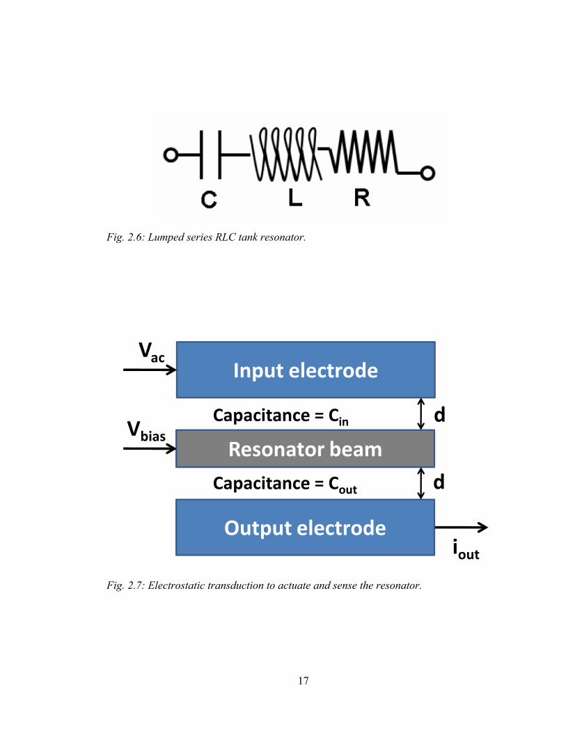
A lumped electrical LCR model of the MEMS resonator is shown in Fig. 2.6. Here we
will discuss about the method to actuate and sense the micro-mechanical resonator. The
electrostatic transduction is used to actuate the resonator beams by applying AC input
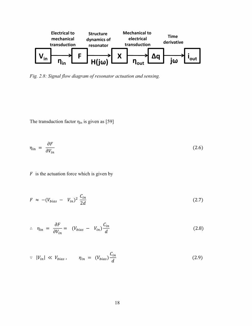
stimulus to the input electrode (Fig. 2.7). The principle of actuation and sense is the
electrostatic attraction force that exists between a parallel plate capacitor. Fig. 2.8
shows an AC signal flow diagram for an electrostatically actuated and sensed MEMS
resonator. The AC input voltage (Vin) applied on the input electrode is converted into
the input force (F) due to electrical to mechanical capacitive transduction (ηin) as shown
in Fig. 2.8. The force causes the oscillation of the resonator beam. When the frequency
of the AC input voltage becomes equal to the natural frequency of the resonator beam,
the beam starts resonating with maximum amplitude, resulting into charge modulation
in the output electrode giving rise to output current (iout) as shown in Fig. 2.8.
17
Fig. 2.6: Lumped series RLC tank resonator.
Fig. 2.7: Electrostatic transduction to actuate and sense the resonator.
Resonator beam
Output electrode
dCapacitance = Cin
Input electrode
Capacitance = Cout d
Vac
Vbias
iout
18
Fig. 2.8: Signal flow diagram of resonator actuation and sensing.
The transduction factor ηin is given as [59]
η 2.6
is the actuation force which is given by
2 2.7
η 2.8
| | , 2.9
Vin
Mechanical to electrical
transduction
ηinF
H(jω)X
ηout∆q
Time derivative
jωiout
Structure dynamics ofresonator
Electrical tomechanicaltransduction
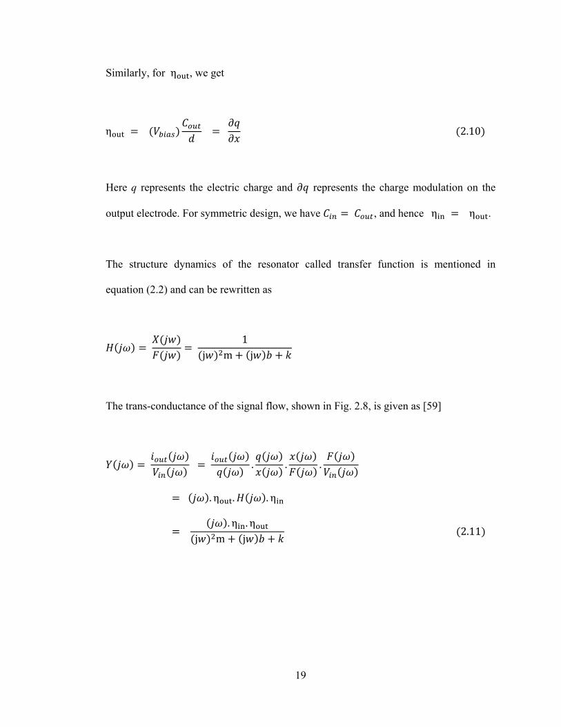
19
Similarly, for η , we get
η 2.10
Here q represents the electric charge and represents the charge modulation on the
output electrode. For symmetric design, we have , and hence η η .
The structure dynamics of the resonator called transfer function is mentioned in
equation (2.2) and can be rewritten as
1
j m j
The trans-conductance of the signal flow, shown in Fig. 2.8, is given as [59]
. . .
. η . . η
. η . η
j m j 2.11
20
At resonance, the above expression becomes
.
. √
1
2.12
where Rx is called motional resistance.
The output current is dependent on the motional resistance which in-turn is dependent
on the quality factor of the resonator, capacitance, gap between the electrodes and the
beam, stiffness and mass of the resonator. It is desired to have high output current for
better signal characteristics of the resonator frequency.
2.3 Temperature Stability
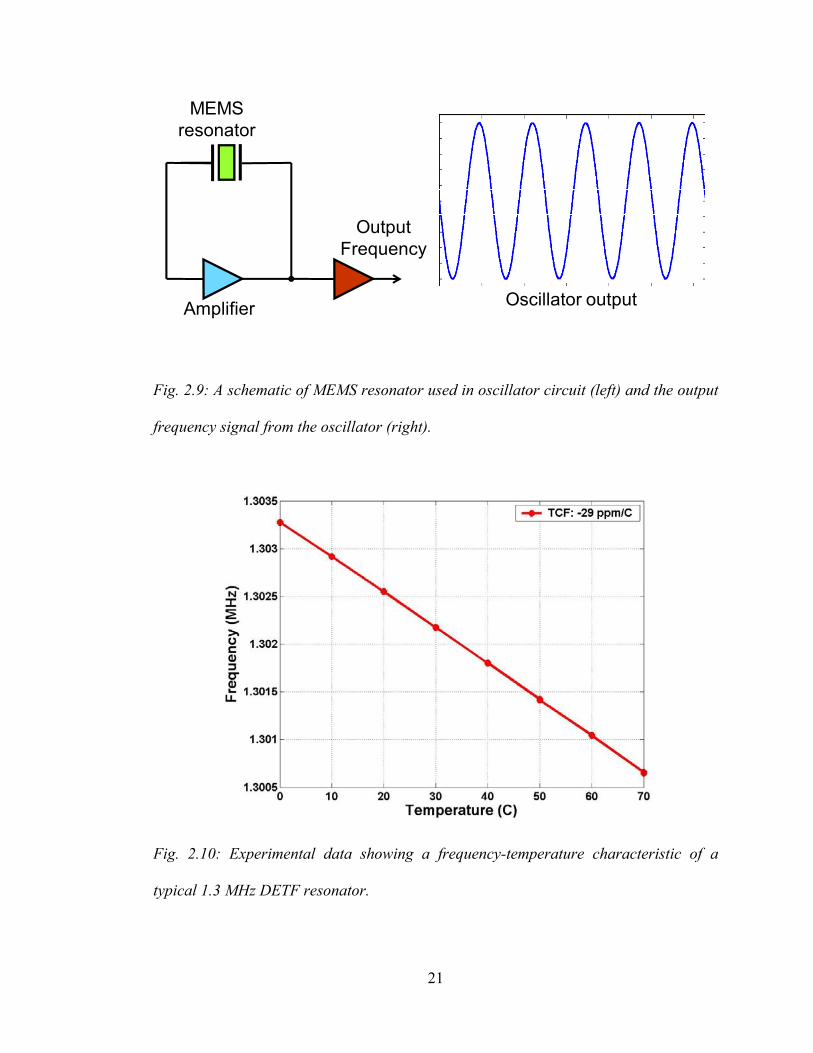
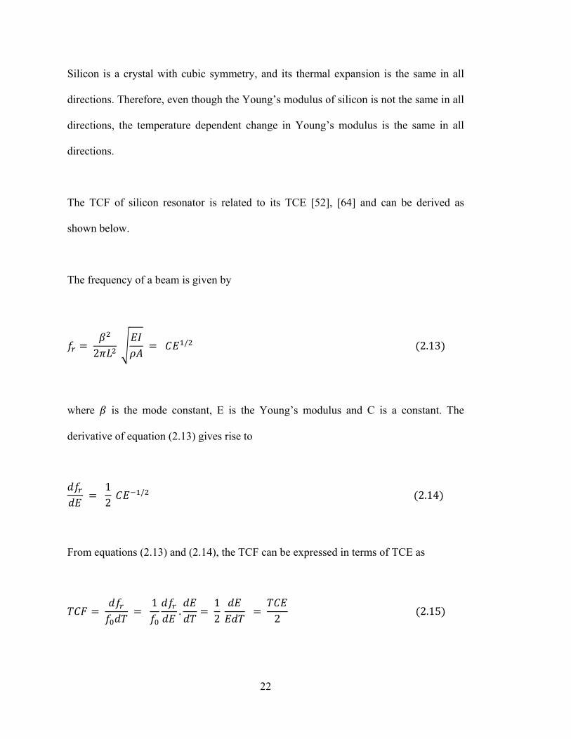
The DETF resonator described in the previous section is used in the oscillator circuit to
generate continuous frequency signal (Fig. 2.9). However, this frequency changes with
the temperature as shown in Fig. 2.10. The temperature dependence of the resonator
frequency is referred as TCF, an abbreviation of Temperature Coefficient of Frequency.
An uncompensated resonator exhibit a TCF of approximately -29 ppm/°C (Fig. 2.10).
The primary reason of such a high TCF of silicon resonator is the temperature
dependence of its material characteristic. The change in Young’s modulus of silicon
with temperature, the TCE, is approximately -63 ppm/°C at normal operating
temperatures [60] – [63].
21
Fig. 2.9: A schematic of MEMS resonator used in oscillator circuit (left) and the output
frequency signal from the oscillator (right).
Fig. 2.10: Experimental data showing a frequency-temperature characteristic of a
typical 1.3 MHz DETF resonator.
MEMSresonator
Amplifier
OutputFrequency
Oscillator output
22
Silicon is a crystal with cubic symmetry, and its thermal expansion is the same in all
directions. Therefore, even though the Young’s modulus of silicon is not the same in all
directions, the temperature dependent change in Young’s modulus is the same in all
directions.
The TCF of silicon resonator is related to its TCE [52], [64] and can be derived as
shown below.
The frequency of a beam is given by
2 / 2.13
where is the mode constant, E is the Young’s modulus and C is a constant. The
derivative of equation (2.13) gives rise to
12 / 2.14
From equations (2.13) and (2.14), the TCF can be expressed in terms of TCE as
1
. 12 2 2.15
23
From equation (2.15), the TCF of the silicon resonator can be estimated to be
approximately -31 ppm/°C. However, there is a marginal effect of dimensional change
on the TCF of the silicon resonator. The dimensions of the resonator change with the
temperature due to thermal expansion. Silicon has an isotropic coefficient of thermal
expansion (CTE, or ), at room temperature of approximately 2.6 ppm/°C [65] – [67],
and that value increases with increasing temperature. The effect of on the TCF of the
resonator can be evaluated in the similar way as described for TCE and can be given as
2 2.16
The effect of thermal expansion on the resonator frequency is /2 and is approximately
+1.3 ppm/°C. The final TCF of the resonator, taking both TCE and into account,
comes to approximately -30 ppm/°C, which is close to the experimental TCF
measurement shown in Fig. 2.10.
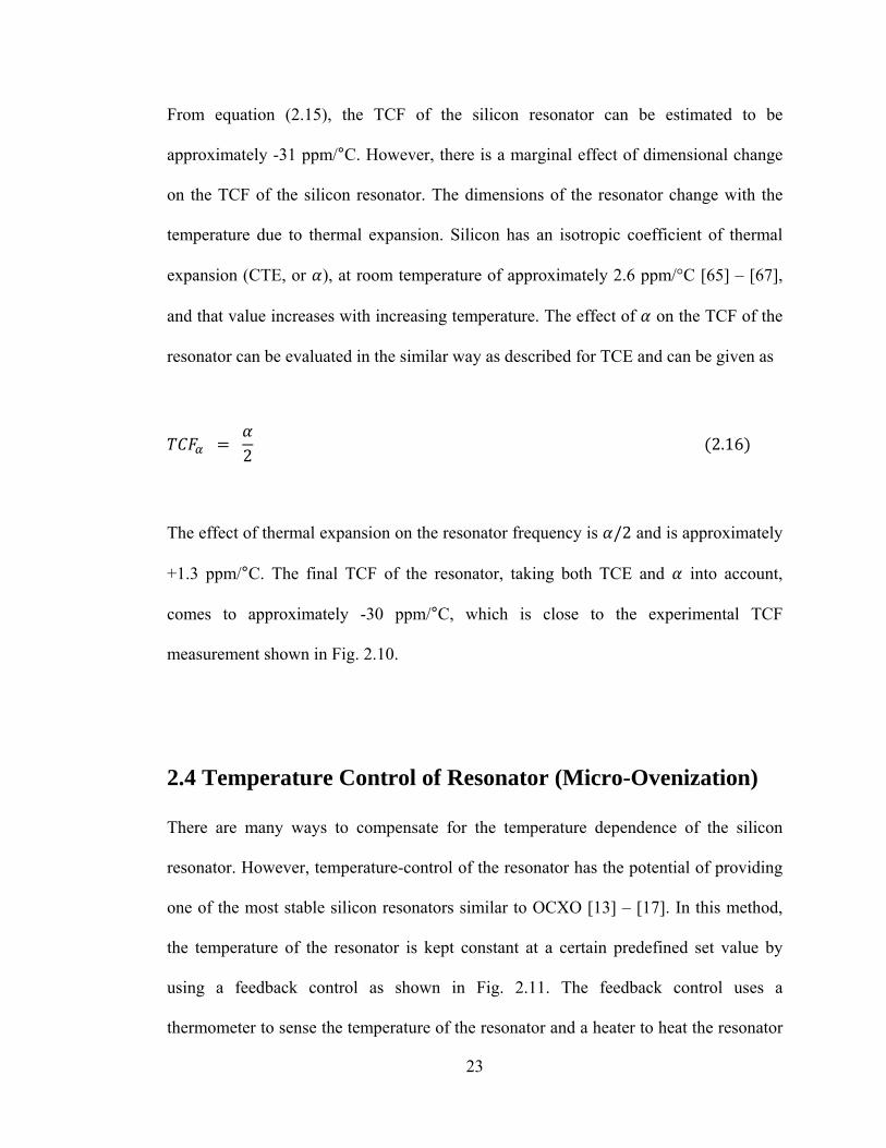
2.4 Temperature Control of Resonator (Micro-Ovenization)
There are many ways to compensate for the temperature dependence of the silicon
resonator. However, temperature-control of the resonator has the potential of providing
one of the most stable silicon resonators similar to OCXO [13] – [17]. In this method,
the temperature of the resonator is kept constant at a certain predefined set value by
using a feedback control as shown in Fig. 2.11. The feedback control uses a
thermometer to sense the temperature of the resonator and a heater to heat the resonator
24
in order to keep its temperature constant and as stable as possible. However, an external
temperature sensor exhibit thermal lag due to a physical separation between the
thermometer and the resonator. Similarly, the heater has to be close to the resonator and
provide heating only to the resonator without losing much heat to the surrounding in
order to have low power consumption and small thermal time constant.
Fig. 2.11: Schematic of feedback control of the resonator using an external
thermometer and a heater.
resonator
Feedback Control
Thermometer
Oven
Heater
25
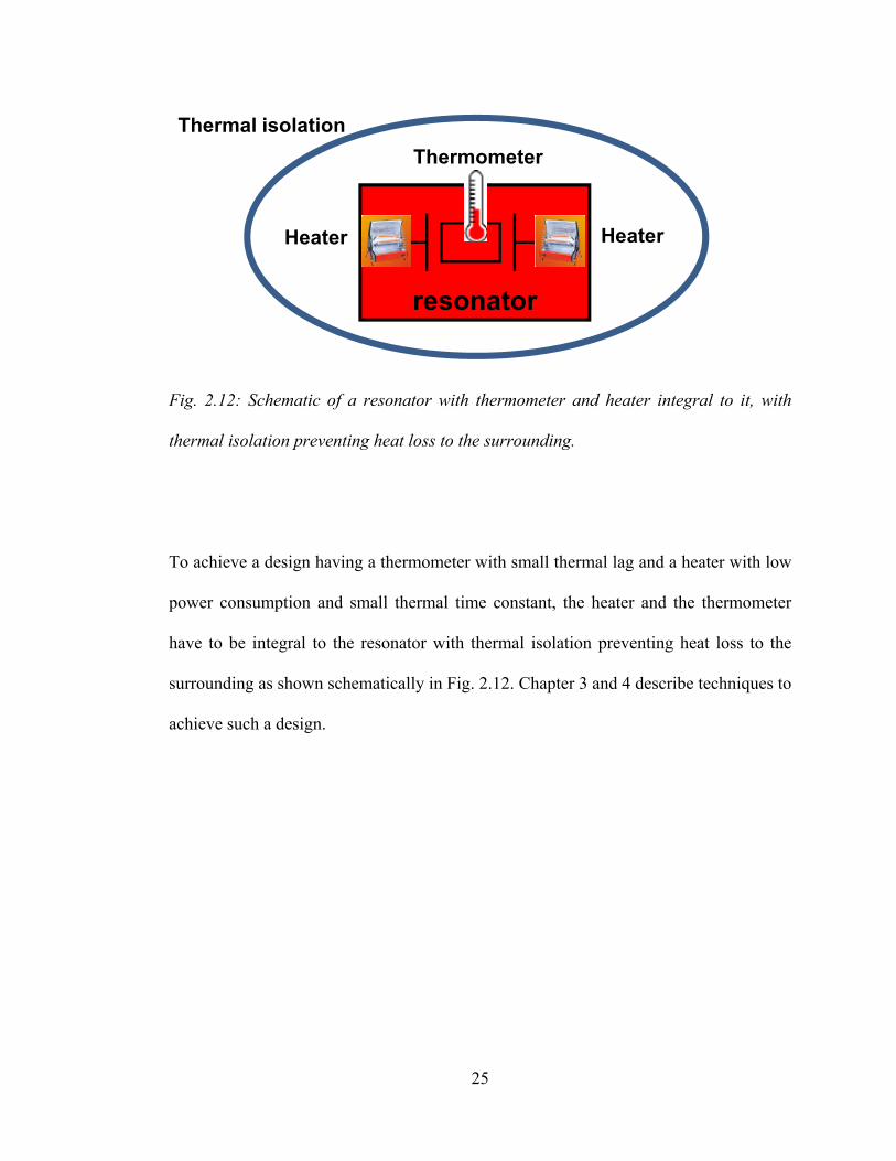
Fig. 2.12: Schematic of a resonator with thermometer and heater integral to it, with
thermal isolation preventing heat loss to the surrounding.
To achieve a design having a thermometer with small thermal lag and a heater with low
power consumption and small thermal time constant, the heater and the thermometer
have to be integral to the resonator with thermal isolation preventing heat loss to the
surrounding as shown schematically in Fig. 2.12. Chapter 3 and 4 describe techniques to
achieve such a design.
resonator
Thermometer
Heater Heater
Thermal isolation

26
27
Chapter 3
Beat Frequency Thermometry
A digital temperature sensing technique using a complementary metal oxide
semiconductor (CMOS) compatible encapsulated micromechanical resonator is
presented. This technique leverages our ability to select the temperature dependence of
the resonant frequency for micromechanical silicon resonators by adjusting the relative
thickness of a SiO2 compensating layer. A dual-resonator design is described that
includes a pair of resonators with differential temperature compensations so that the
difference between the two resonant frequencies is a sensitive function of temperature.
We demonstrate a temperature resolution of approximately 0.008 °C for 1 s averaging
time, which is better than that of the best CMOS temperature sensors available today.
At the same time, the beat frequency thermometry is highly effective in the temperature
compensation of the resonator as it eliminates the thermal lag.
3.1 Introduction
The frequency of silicon resonators varies strongly with temperature [52], [64], [68].
This characteristic of a silicon resonator, which is disadvantageous in general, can be
used to measure temperature. However, the biggest problem lies in measuring the
temperature-dependent frequency without using any external frequency references. In
28
this work, we present a novel dual-resonator design with a composite Si–SiO2 structure
[69], [70], which provides a temperature-dependent signal and a reference for
measuring the signal. This concept for digital thermometry relies on the application of
the basic mechanics of resonator design, as well as the materials physics that provides
different temperature coefficients of stiffness for silicon and SiO2. In this design, we
build a pair of resonators with different cross-sectional dimensions, but with similar
frequencies, by scaling the lengths. After formation of an oxide compensation layer
over all surfaces, we obtain a pair of resonators with similar frequencies but with
different temperature coefficients of frequency. The difference frequency, called beat
frequency, between these two references has a much higher sensitivity to temperature,
and it can be “internally counted” using one of the resonators as a reference [71], [72].
Taken together, the physics of compensated micromechanical resonators and the ultra-
stable resonator encapsulation process provides path toward a unique, CMOS-
compatible digital temperature sensor with potential for much better performance than
existing digital temperature sensors based on diode thermometers.
3.2 Beat Frequency Generation
The multiplication of the two oscillator signals at frequencies f1 and f2 yields signals at
frequencies f1 + f2 and f1 – f2 as per Eq. (3.1). The difference frequency f1 – f2 is called
the beat frequency and is obtained after discarding the higher frequency through the
second order low-pass filter as shown in Fig. 3.1.
2 . 2 12 2 2 3.1
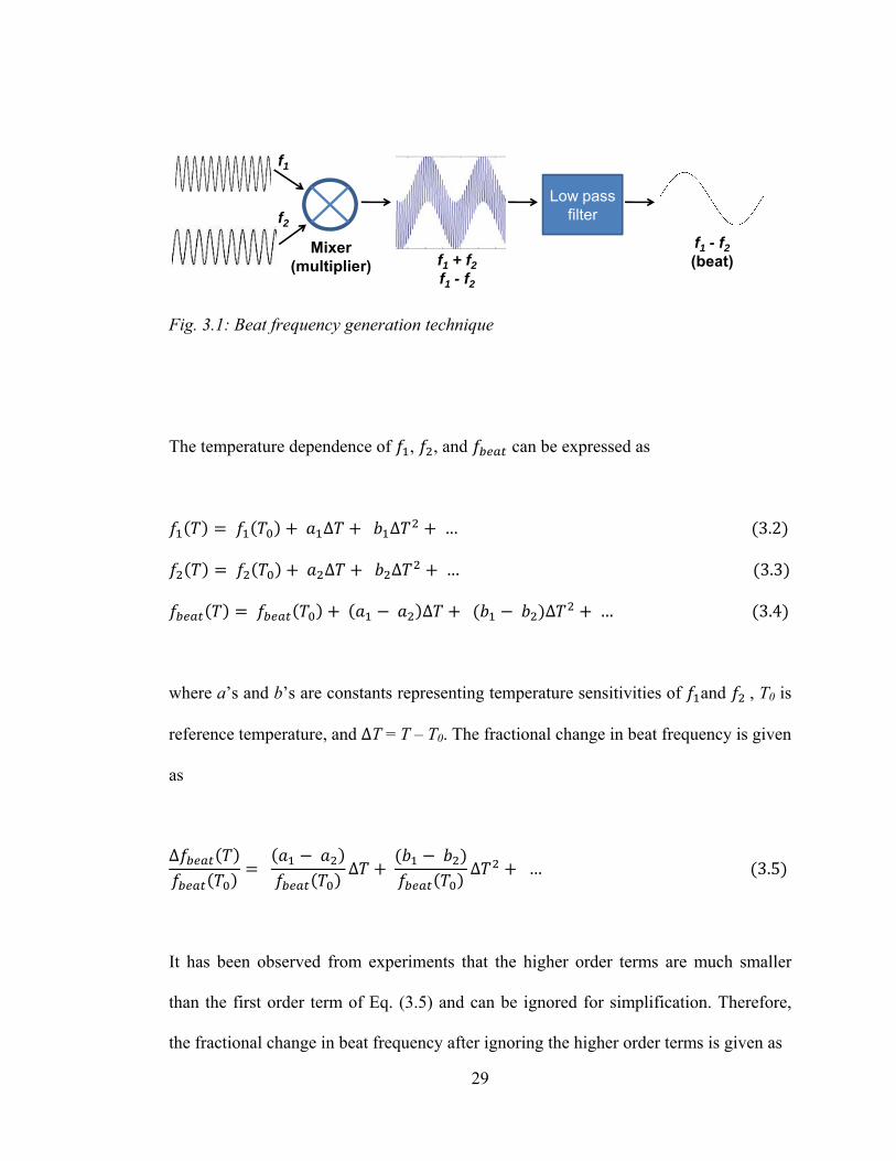
29
Fig. 3.1: Beat frequency generation technique
The temperature dependence of , , and can be expressed as
∆ ∆ … 3.2
∆ ∆ … 3.3
∆ ∆ … 3.4
where a’s and b’s are constants representing temperature sensitivities of and , T0 is
reference temperature, and ∆T = T – T0. The fractional change in beat frequency is given
as
∆
∆
∆ … 3.5
It has been observed from experiments that the higher order terms are much smaller
than the first order term of Eq. (3.5) and can be ignored for simplification. Therefore,
the fractional change in beat frequency after ignoring the higher order terms is given as
Mixer(multiplier) f1 + f2
f1 - f2
Low pass filter
f1 - f2(beat)
f1
f2
30
∆
∆ ∆ 3.6
where is the first order TCf (ppm/°C) of the beat frequency.
The equation (3.6) shows that the temperature dependence (TCF) of beat frequency is
directly proportional to the difference in TCF’s of the frequencies and . The TCF of
the beat frequency increases with the increase in and decrease in the
absolute value of . To obtain a beat frequency with large temperature sensitivity,
the difference in TCf of f1 and f2 should be as large as possible and at the same time the
beat frequency should be as small as feasible. The fundamental requirement of the beat
frequency thermometry is to have two different frequency sources with different
temperature sensitivities.
3.3 Si-SiO2 Composite Resonator
One way of realizing a resonator with different temperature sensitivity is to form a
composite resonator. Our lab came up with a novel technique of forming a Si-SiO2
composite resonator [70]. The temperature dependence of the silicon resonator
frequency is mainly related to its material properties as shown in equation (2.15) and
can be rewritten here as
31
2
where stands for temperature coefficient of Young’s modulus of silicon.
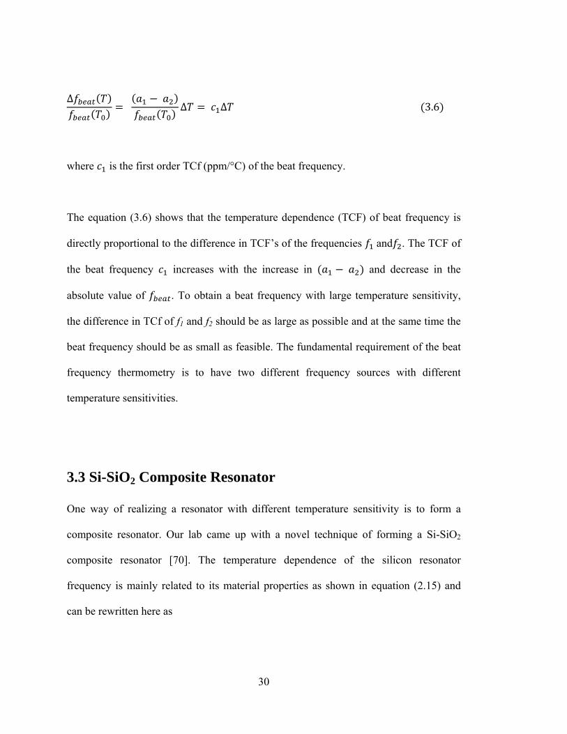
The is approximately -60 ppm/°C. In other words, Si becomes soft with the
increase of temperature. On the other hand, if we take a look at the properties of SiO2, it
becomes hard with the increase of temperature (Fig. 3.2). By combining the material
properties of both Si and SiO2, it is possible to alter or reduce the
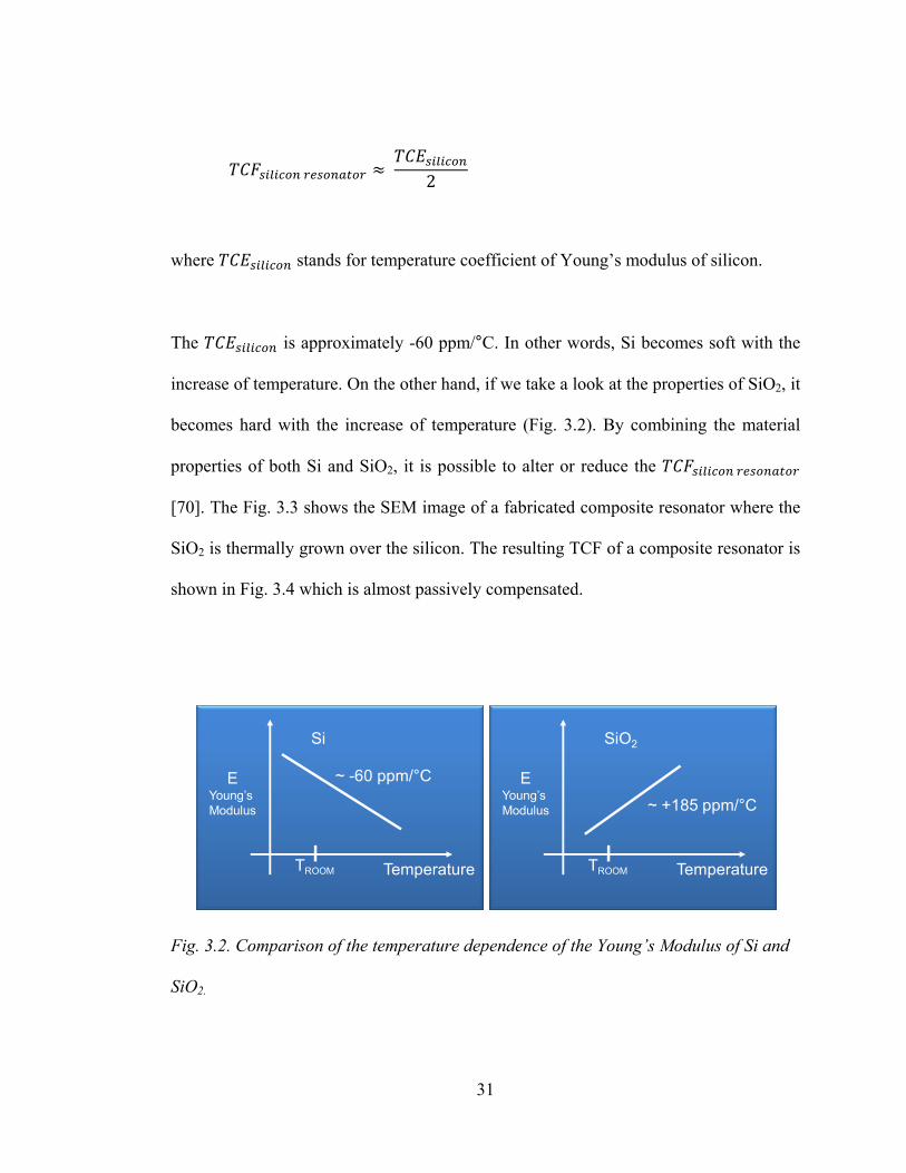
[70]. The Fig. 3.3 shows the SEM image of a fabricated composite resonator where the
SiO2 is thermally grown over the silicon. The resulting TCF of a composite resonator is
shown in Fig. 3.4 which is almost passively compensated.
Fig. 3.2. Comparison of the temperature dependence of the Young’s Modulus of Si and
SiO2.
Temperature
EYoung’s Modulus
SiO2
TROOM
~ +185 ppm/°C
Temperature
EYoung’s Modulus
Si
TROOM
~ -60 ppm/°C
32
Fig. 3.3. (a) SEM image of a composite silicon resonator beam with the thermally
grown SiO2 layer. (b) Enlarged view.
Fig. 3.4. Experimental data showing the comparison of TCF of bare silicon and the
composite silicon.
-40 -20 0 20 40 60 80 100 120-1000
0
1000
2000
3000
4000
Temperature (°C)
Δ f /
f 0 ( P
PM
)
f1 (Passively Temperature Compensated)
f1 (Uncompensated TCF: -29 ppm /°C)
Si - SiO2Composite
Si
33
3.4 Dual-Resonator Design
A candidate dual-resonator design having two mechanically coupled double-ended
tuning fork (DETF) type resonators is shown in Fig. 3.5. These DETF resonators consist
of composite resonator beams of silicon (Si) and silicon dioxide (SiO2). The thickness
of the thermally grown SiO2 coating over the Si beam is approximately 0.33 μm for
both resonators (Fig. 3.5). The silicon-to-oxide ratio of the beams for the two DETF
structures is designed to achieve two different temperature coefficients of frequency
(TCf), while keeping the two frequencies close together. These devices were fabricated
using a CMOS-compatible wafer scale encapsulation process [57], [58]. A scanning
electron microscopy view of the thermally grown SiO2 coating over the Si beam [70] is
shown in Fig. 3.3 and Fig. 3.6.
The beam cross-sections of the two resonators in the dual resonator design and the ratio
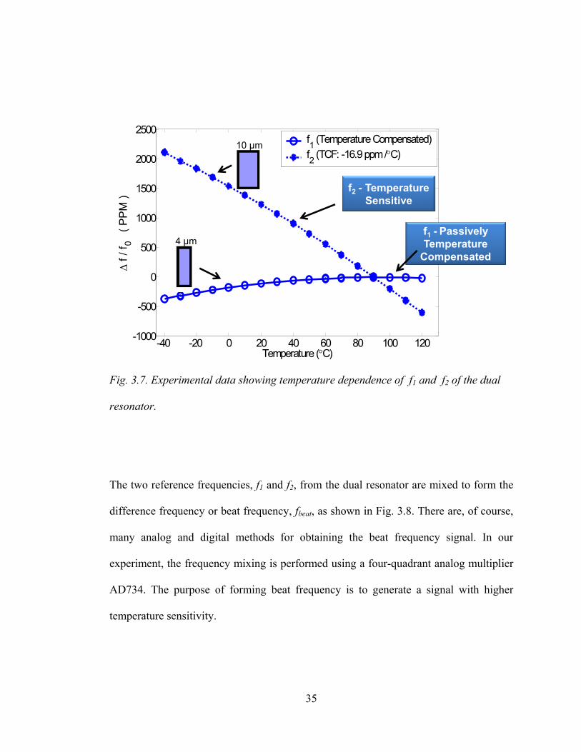
of Si to SiO2 thicknesses dictate the TCF of the two frequencies signal f1 and f2
(Fig. 3.7). The beam with 10μm thickness has less effect of 0.33μm thick SiO2 and
hence has higher TCF compared to the beam with 4μm thickness having 0.33μm thick
SiO2 as shown in Fig. 3.7.
34
Fig. 3.5. Dual resonator design showing the two DETF resonators with different cross
sections having the same SiO2 thicknesses. Both the resonators are anchored at a
common point to ensure uniform temperature across the entire structure of the dual
resonator.
Fig. 3.6. SEM image of the composite resonator with 0.33μm SiO2 coating over the Si
beam.
SiO2
Silicon
Poly Si
SiO2
Al
SiliconBeam
Poly Silicon Encapsulation
Silicon Dioxide (~ 0.33µm)
Dri
veE
lect
rode
110
100
SiliconHandle
35
Fig. 3.7. Experimental data showing temperature dependence of f1 and f2 of the dual
resonator.
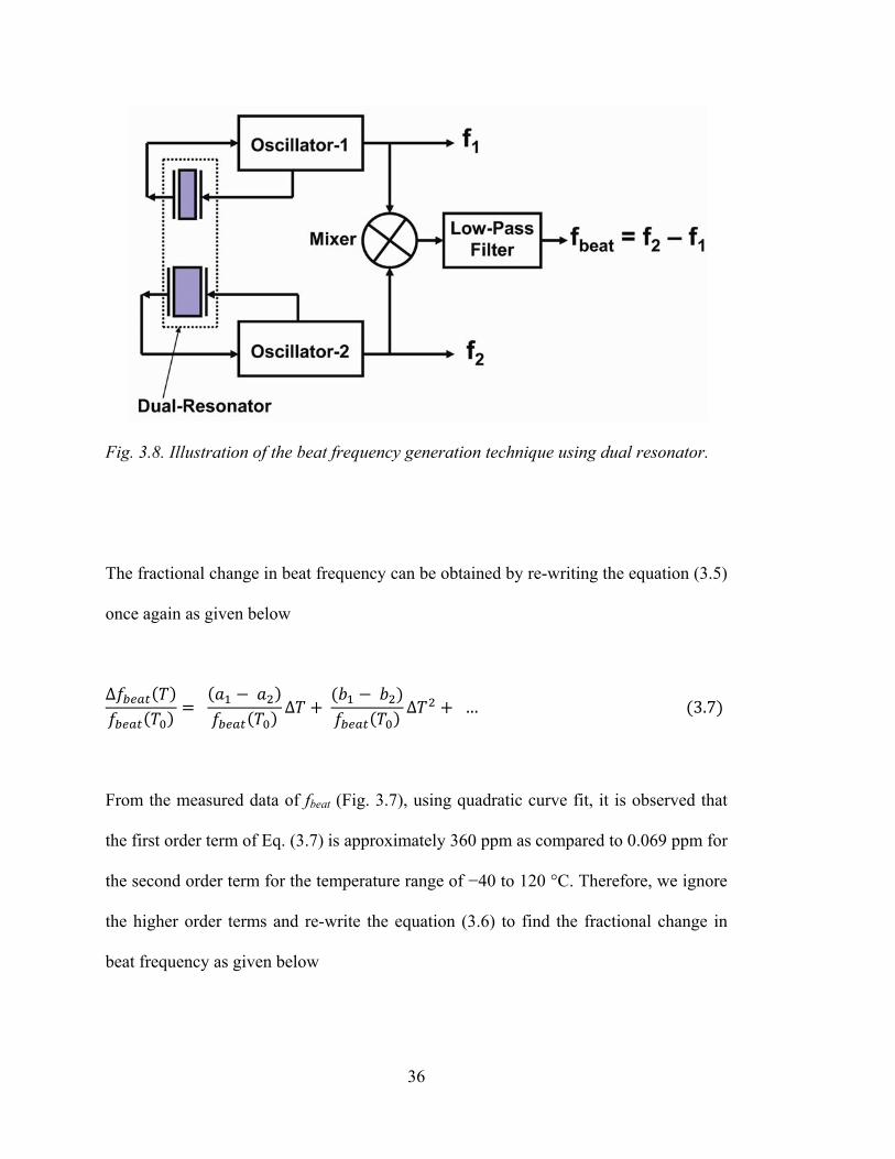
The two reference frequencies, f1 and f2, from the dual resonator are mixed to form the
difference frequency or beat frequency, fbeat, as shown in Fig. 3.8. There are, of course,
many analog and digital methods for obtaining the beat frequency signal. In our
experiment, the frequency mixing is performed using a four-quadrant analog multiplier
AD734. The purpose of forming beat frequency is to generate a signal with higher
temperature sensitivity.
-40 -20 0 20 40 60 80 100 120-1000
-500
0
500
1000
1500
2000
2500
Temperature (°C)
Δ f /
f 0 (
PP
M )
f1 (Temperature Compensated)f2 (TCF: -16.9 ppm /°C)
f1 - Passively Temperature
Compensated
f2 - Temperature Sensitive
10 μm
4 μm
36
Fig. 3.8. Illustration of the beat frequency generation technique using dual resonator.
The fractional change in beat frequency can be obtained by re-writing the equation (3.5)
once again as given below
∆
∆
∆ … 3.7
From the measured data of fbeat (Fig. 3.7), using quadratic curve fit, it is observed that
the first order term of Eq. (3.7) is approximately 360 ppm as compared to 0.069 ppm for
the second order term for the temperature range of −40 to 120 °C. Therefore, we ignore
the higher order terms and re-write the equation (3.6) to find the fractional change in
beat frequency as given below
37
∆
∆ ∆ 3.8
The dual resonator described in this work produces reference frequencies f1 and f2 of
approximately 1.37 and 1.45 MHz, respectively, resulting in a beat frequency fbeat of
approximately 75 kHz. The resonator with frequency f1 is passively temperature
compensated to first order (Fig. 3.7), while the resonator with frequency f2 has a larger
TCf of −17 ppm/ °C. We obtain a pair of resonators with the same frequency but with
different TCfs by scaling one design with respect to the other and growing the same
thickness of oxide on both. Since the frequencies of the dual resonator are close
together, the beat frequency is exceptionally sensitive to temperature changes, as per
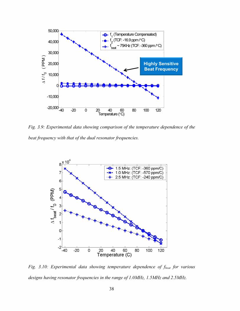
Eq. (3.8), and nearly linear, as shown in Fig. 3.9, with a TCf of approximately −360
ppm/ °C. The high sensitivity and the linearity of the beat frequencies have been
verified on several devices as shown in Fig. 3.10.
3.5 Sensor Application
The dual resonator based beat frequency temperature sensor described above can be
used both for the temperature compensation of the resonator as well as for the general
purpose CMOS digital temperature sensor. For the temperature compensation, the beat
frequency acts as a self-temperature sensor of the resonator, thereby avoiding any
thermal lag associated with an external temperature sensor. Fig. 3.11 describes the
significance of the beat frequency thermometry for sensing the resonator temperature
compared to an external temperature sensor.
38
Fig. 3.9: Experimental data showing comparison of the temperature dependence of the
beat frequency with that of the dual resonator frequencies.
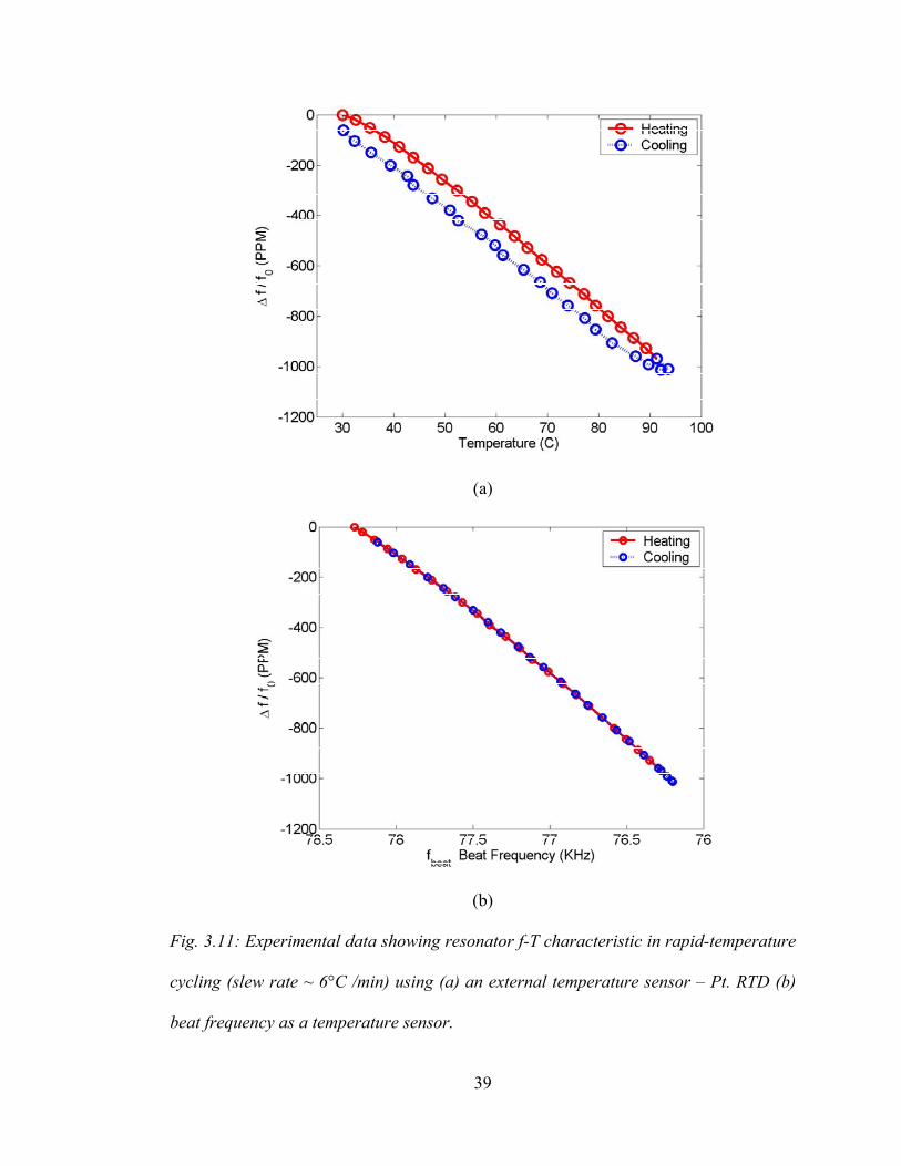
Fig. 3.10: Experimental data showing temperature dependence of fbeat for various
designs having resonator frequencies in the range of 1.0MHz, 1.5MHz and 2.5MHz.
-40 -20 0 20 40 60 80 100 120-20,000
-10,000
0
10,000
20,000
30,000
40,000
50,000
Temperature (°C)
Δ f /
f 0 (
PP
M )
f1 (Temperature Compensated)f2 (TCF: -16.9 ppm /°C)fbeat ~ 75KHz (TCF: -360 ppm /°C)
Highly Sensitive Beat Frequency
39
(a)
(b)
Fig. 3.11: Experimental data showing resonator f-T characteristic in rapid-temperature
cycling (slew rate ~ 6°C /min) using (a) an external temperature sensor – Pt. RTD (b)
beat frequency as a temperature sensor.
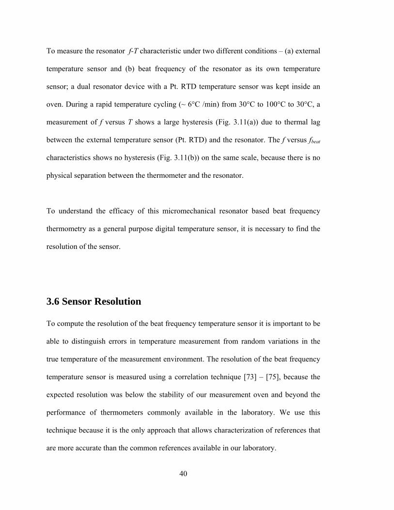
40
To measure the resonator f-T characteristic under two different conditions – (a) external
temperature sensor and (b) beat frequency of the resonator as its own temperature
sensor; a dual resonator device with a Pt. RTD temperature sensor was kept inside an
oven. During a rapid temperature cycling (~ 6°C /min) from 30°C to 100°C to 30°C, a
measurement of f versus T shows a large hysteresis (Fig. 3.11(a)) due to thermal lag
between the external temperature sensor (Pt. RTD) and the resonator. The f versus fbeat
characteristics shows no hysteresis (Fig. 3.11(b)) on the same scale, because there is no
physical separation between the thermometer and the resonator.
To understand the efficacy of this micromechanical resonator based beat frequency
thermometry as a general purpose digital temperature sensor, it is necessary to find the
resolution of the sensor.
3.6 Sensor Resolution
To compute the resolution of the beat frequency temperature sensor it is important to be
able to distinguish errors in temperature measurement from random variations in the
true temperature of the measurement environment. The resolution of the beat frequency
temperature sensor is measured using a correlation technique [73] – [75], because the
expected resolution was below the stability of our measurement oven and beyond the
performance of thermometers commonly available in the laboratory. We use this
technique because it is the only approach that allows characterization of references that
are more accurate than the common references available in our laboratory.
41
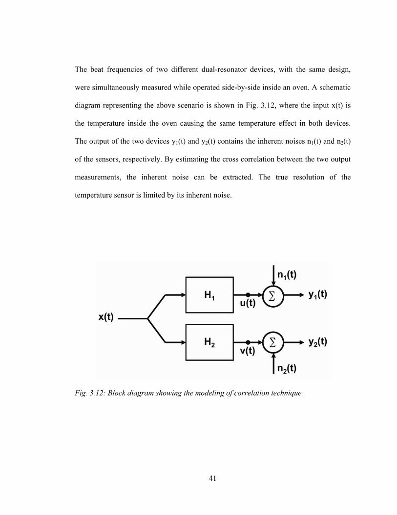
The beat frequencies of two different dual-resonator devices, with the same design,
were simultaneously measured while operated side-by-side inside an oven. A schematic
diagram representing the above scenario is shown in Fig. 3.12, where the input x(t) is
the temperature inside the oven causing the same temperature effect in both devices.
The output of the two devices y1(t) and y2(t) contains the inherent noises n1(t) and n2(t)
of the sensors, respectively. By estimating the cross correlation between the two output
measurements, the inherent noise can be extracted. The true resolution of the
temperature sensor is limited by its inherent noise.
Fig. 3.12: Block diagram showing the modeling of correlation technique.
42
The inherent noise of the sensor is nothing but the variance of the noise n1 ( or n2
( . It is assumed that the noises of the two devices are uncorrelated, that is
0 3.9
From the Fig. 3.12, we can write [74], [75]
| | 3.10
| | 3.11
| | | | 3.12
where is the covariance between y1 and y2, and is the variance of y1
and y2 respectively. | | and | | are the transfer function, in this case TCF’s, of the
sensor 1 and 2 respectively. An important term, called correlation coefficient
between the two measurements y1(t) and y2(t), is given by [74], [75]
3.13
From equations (3.9) to (3.13), the intrinsic noise in device 1 can be derived as
1 | |
3.14
43
For the dual resonator, the second term in the bracket in equation (3.14) results into
approximately and hence the noise variance can be simplified as
1 3.15
In terms of deviation, equation (3.15) becomes
1 3.16
where is the deviation in the output signal of device 1 and is the correlation
coefficient between the measured signals of the two devices. Measurements of fbeat of
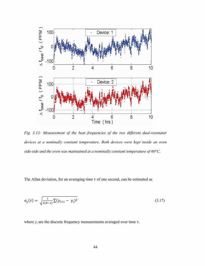
both devices were taken over a period of 10 hours. As can be seen in Fig. 3.13, both
signals are tracking the small variations in the temperature inside the oven (~ 0.3 °C),
and that most of the variations in the individual signals are present in both sensors.
Since the resonator based oscillators can have various types of noise other than white
noise, an IEEE recommended Allan deviation [76] has been used to calculate the
deviation in the measurements. The classical standard deviation for such measurements
depends on the number of data points and hence may not converge [76]. However, if the
oscillator exhibits only white noise then the Allan deviation and the classical standard
deviation will give the same result.
44
Fig. 3.13: Measurement of the beat frequencies of the two different dual-resonator
devices at a nominally constant temperature. Both devices were kept inside an oven
side-side and the oven was maintained at a nominally constant temperature of 60°C.
The Allan deviation, for an averaging time of one second, can be estimated as
∑ (3.17)
where yi are the discrete frequency measurements averaged over time .
45
Fig. 3.14: Evaluation of the Allan deviation of the measured beat frequency data and its
noise.
Ignoring the dead time between the two consecutive measurements, the Allan deviation
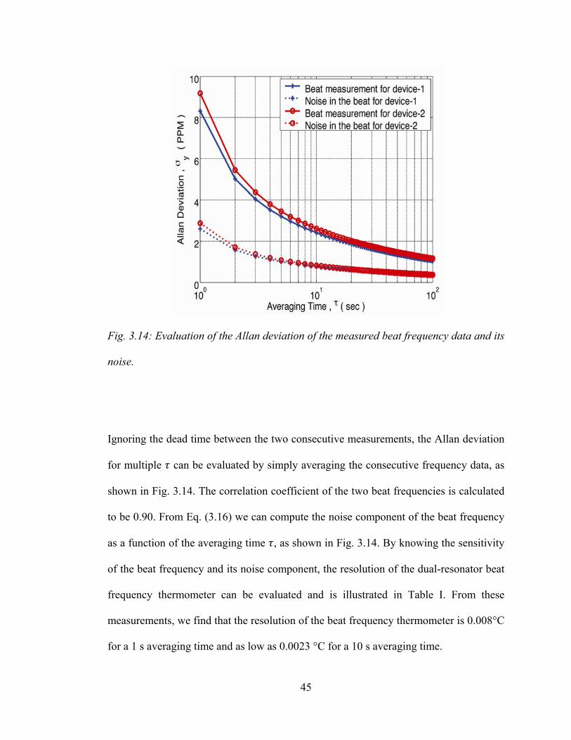
for multiple can be evaluated by simply averaging the consecutive frequency data, as
shown in Fig. 3.14. The correlation coefficient of the two beat frequencies is calculated
to be 0.90. From Eq. (3.16) we can compute the noise component of the beat frequency
as a function of the averaging time , as shown in Fig. 3.14. By knowing the sensitivity
of the beat frequency and its noise component, the resolution of the dual-resonator beat
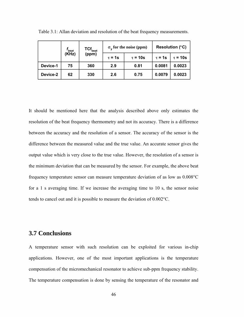
frequency thermometer can be evaluated and is illustrated in Table I. From these
measurements, we find that the resolution of the beat frequency thermometer is 0.008°C
for a 1 s averaging time and as low as 0.0023 °C for a 10 s averaging time.
46
Table 3.1: Allan deviation and resolution of the beat frequency measurements.
It should be mentioned here that the analysis described above only estimates the
resolution of the beat frequency thermometry and not its accuracy. There is a difference
between the accuracy and the resolution of a sensor. The accuracy of the sensor is the
difference between the measured value and the true value. An accurate sensor gives the
output value which is very close to the true value. However, the resolution of a sensor is
the minimum deviation that can be measured by the sensor. For example, the above beat
frequency temperature sensor can measure temperature deviation of as low as 0.008°C
for a 1 s averaging time. If we increase the averaging time to 10 s, the sensor noise
tends to cancel out and it is possible to measure the deviation of 0.002°C.
3.7 Conclusions
A temperature sensor with such resolution can be exploited for various in-chip
applications. However, one of the most important applications is the temperature
compensation of the micromechanical resonator to achieve sub-ppm frequency stability.
The temperature compensation is done by sensing the temperature of the resonator and
0.00230.00790.752.633062Device-2
0.00230.00810.812.936075Device-1
τ = 10sτ = 1sτ = 10sτ = 1s
Resolution (°C)σy for the noise (ppm)TCfbeat(ppm)
fbeat(KHz)
47
then stabilizing the frequency by using feedback control logic. Since the dual-resonator
beat frequency thermometry is inherent to the resonator, this technique of temperature
sensing is ideal for the temperature compensation of micromechanical resonators.
Similar techniques have been used in the past to achieve the frequency stability of the
order of 10-9 in the quartz resonators.
Significant improvements in the performance of this sensor are possible by designing
high-frequency low phase noise dual resonators, resulting in a sensor resolution of
better than 0.001 °C, which would enable significant improvements in temperature
compensation of a very wide spectrum of analog and digital systems. It is also possible
to enhance the temperature sensitivity of the beat frequency by more closely matching
the initial frequencies of the two resonators. In the example demonstrated here, the
mismatch between frequencies is of the order of 6% and arises from fabrication
uncertainties in our process. A more stable process executed in a CMOS manufacturing
line can be expected to achieve frequency matching to better than 1%, resulting in a
very high temperature sensitive beat frequency, leading to improved performance of the
sensor in measuring the smallest change in temperature above its resolution.
Now that we have found the technique for a lag-free thermometry, we need to come up
with a method for an efficient thermal isolation of the resonator. Next chapter describes
an in-built heater based thermal isolation technique.

48
49
Chapter 4
Thermal Isolation of MEMS Resonator
This chapter presents an in-chip thermal-isolation technique for a micro-ovenized
microelectromechanical-system resonator using a single DETF resonator. Resonators
with a micro-oven can be used for high precision feedback control of temperature to
compensate for the temperature dependence of resonator frequency over a wide
temperature range. However, ovenization requires power consumption for heating, and
the thermal time constant must be minimized for effective temperature control. We
demonstrate an efficient local-thermal-isolation mechanism, which can reduce the
power requirement to a few milliwatts and the thermal time constant to a few
milliseconds. In this method, the mechanical suspension of the resonator is modified to
provide thermal isolation and include an integrated resistive heater. This combination
provides mechanical suspension, electrical heating, and thermal isolation in a compact
structure that requires low heating power and has a small thermal time constant. A
power consumption of approximately 12 mW for a 125 °C temperature rise and a
thermal time constant ranging from 7 to 10 ms is reported here, which is approximately
20x and 50x, respectively, lower than the un-isolated MEMS resonator and several
orders of magnitude lower than that of the commercially available ovenized quartz
resonators. A CMOS-compatible wafer-scale encapsulation process is used to fabricate
this device, and the thermal-isolation design is achieved without any modification to the
existing resonator fabrication process.
50
4.1 Introduction
Currently, oven-controlled quartz resonators are used to generate high-precision
frequency references suitable for high-end industry and military standards [13] – [17].
As explained in chapter 2, in this method the resonator is held at a fixed temperature to
compensate for the temperature dependence of the resonator frequency. The extent to
which the resonator is heated depends on the difference between the set point and the
ambient temperature. For an ovenized resonator that is required to operate within a
temperature range of −40 °C to 85 °C, the heating has to cover a range of 125 °C. Due
to the large volume of a conventional quartz-crystal oscillators, which can be up to 1000
mm3 [17], the power consumption for heating can be as much as 10 W with a warm-up
time of approximately 30 min [17], [18], [77], where a warm-up time is defined as the
time required for an oscillator to reach a pre-defined frequency stability. MEMS
technology offers miniaturization to submillimeter scales, which can provide substantial
power reduction [22], [53] – [55], through a micro-oven design.
A micro-oven, in general, constitutes a heater for joule heating and thermal isolation for
reducing heat loss. Micro-oven designs for MEMS devices have been reported before
with few milliwatts of power consumption and a time constant in milliseconds [53] –
[55]. In these designs, a MEMS structure is suspended on a microplatform. The
microplatform is thermally isolated from the substrate and contains separate heater and
sense resistors. Although promising, these designs have limitations in terms of lack of
mechanical stiffness, large thermal mass, and complex fabrication processes. This work
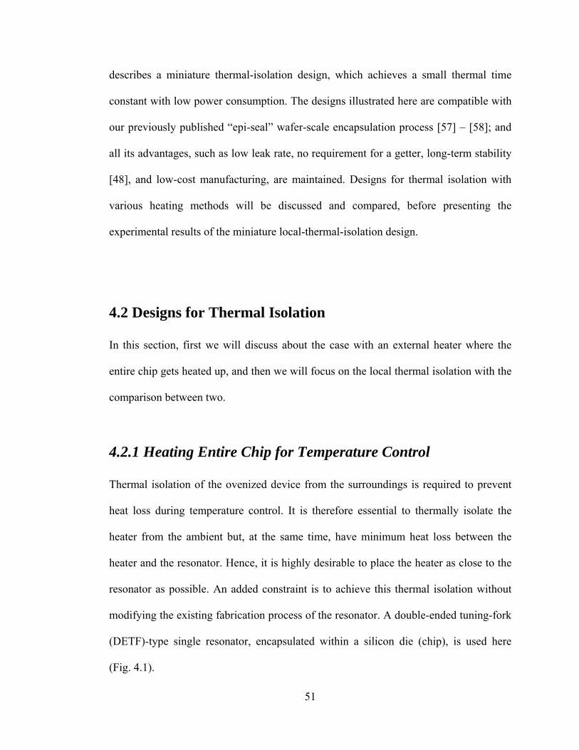
51
describes a miniature thermal-isolation design, which achieves a small thermal time
constant with low power consumption. The designs illustrated here are compatible with
our previously published “epi-seal” wafer-scale encapsulation process [57] – [58]; and
all its advantages, such as low leak rate, no requirement for a getter, long-term stability
[48], and low-cost manufacturing, are maintained. Designs for thermal isolation with
various heating methods will be discussed and compared, before presenting the
experimental results of the miniature local-thermal-isolation design.
4.2 Designs for Thermal Isolation
In this section, first we will discuss about the case with an external heater where the
entire chip gets heated up, and then we will focus on the local thermal isolation with the
comparison between two.
4.2.1 Heating Entire Chip for Temperature Control
Thermal isolation of the ovenized device from the surroundings is required to prevent
heat loss during temperature control. It is therefore essential to thermally isolate the
heater from the ambient but, at the same time, have minimum heat loss between the
heater and the resonator. Hence, it is highly desirable to place the heater as close to the
resonator as possible. An added constraint is to achieve this thermal isolation without
modifying the existing fabrication process of the resonator. A double-ended tuning-fork
(DETF)-type single resonator, encapsulated within a silicon die (chip), is used here
(Fig. 4.1).
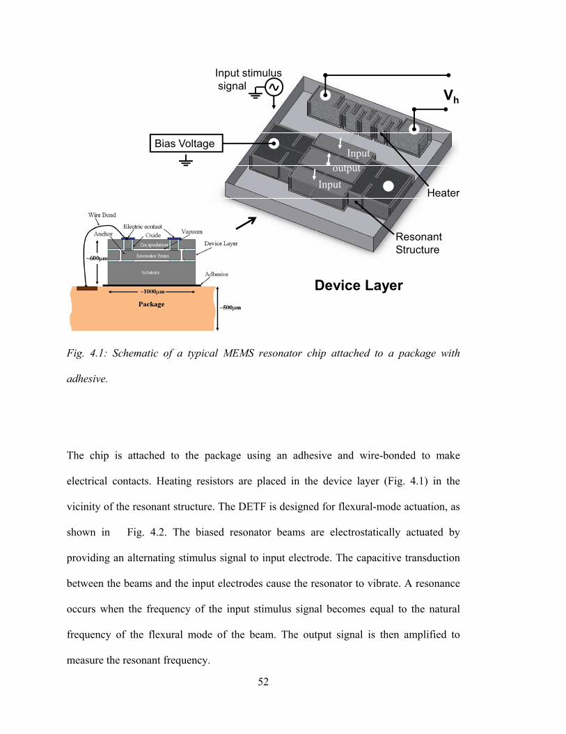
52
Fig. 4.1: Schematic of a typical MEMS resonator chip attached to a package with
adhesive.
The chip is attached to the package using an adhesive and wire-bonded to make
electrical contacts. Heating resistors are placed in the device layer (Fig. 4.1) in the
vicinity of the resonant structure. The DETF is designed for flexural-mode actuation, as
shown in Fig. 4.2. The biased resonator beams are electrostatically actuated by
providing an alternating stimulus signal to input electrode. The capacitive transduction
between the beams and the input electrodes cause the resonator to vibrate. A resonance
occurs when the frequency of the input stimulus signal becomes equal to the natural
frequency of the flexural mode of the beam. The output signal is then amplified to
measure the resonant frequency.
output
Input stimulussignal
Vh
Bias VoltageInput
Input
Resonant Structure
Heater
Device Layer
53
(a)
(b)
Fig. 4.2: (a) Top view schematic of a standard un-isolated DETF-type resonant
structure showing input and output electrodes. (b) FEM simulation of flexural-
vibration mode of a DETF (exaggerated view).
Input ElectrodeBias Voltage
AnchorInput Electrode
Output Electrode
Resonator Beams
Anchor
Bias Voltage
Anchor
Beam Motion
Anchor
54
The power consumption and the thermal time constant can be estimated by using a
simple 1-D lumped-parameter thermal model [78], [79]. The expression for conductive
thermal resistance is given by
4.1
where is the thermal conductivity, is the length, and is the area of cross-section.
Thermal capacitance can be evaluated as
4.2
where is the density, is the volume, and is the specific heat capacity at constant
pressure.
Radiative and convective thermal loss can be found by
1
1
4.3
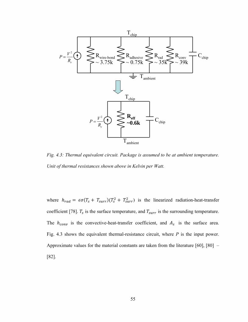
55
Fig. 4.3: Thermal equivalent circuit. Package is assumed to be at ambient temperature.
Unit of thermal resistances shown above in Kelvin per Watt.
where ) is the linearized radiation-heat-transfer
coefficient [78]. is the surface temperature, and is the surrounding temperature.
The is the convective-heat-transfer coefficient, and is the surface area.
Fig. 4.3 shows the equivalent thermal-resistance circuit, where P is the input power.
Approximate values for the material constants are taken from the literature [60], [80] –
[82].
Radhesive~ 0.75k
CchipRrad~ 35k
Rwire-bond~ 3.75keR
VP2
=
Tchip
Tambient
Rconv~ 39k
eRVP
2
= CchipReff~0.6k
Tchip
Tambient
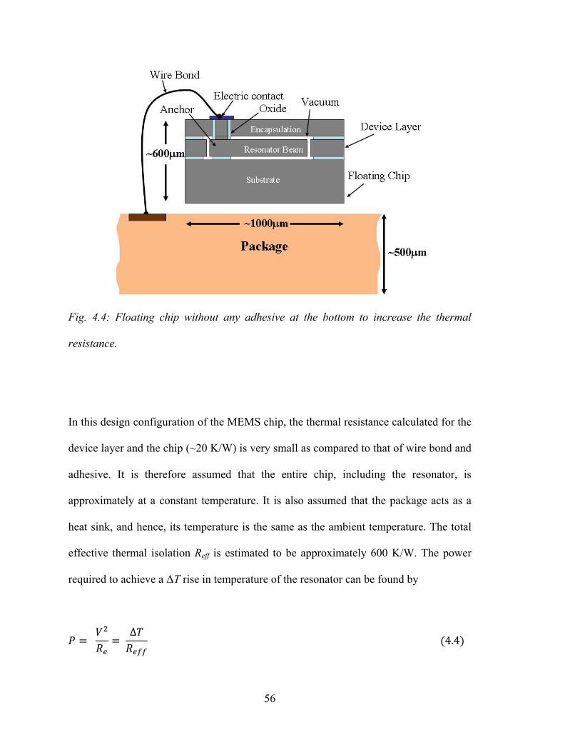
56
Fig. 4.4: Floating chip without any adhesive at the bottom to increase the thermal
resistance.
In this design configuration of the MEMS chip, the thermal resistance calculated for the
device layer and the chip (~20 K/W) is very small as compared to that of wire bond and
adhesive. It is therefore assumed that the entire chip, including the resonator, is
approximately at a constant temperature. It is also assumed that the package acts as a
heat sink, and hence, its temperature is the same as the ambient temperature. The total
effective thermal isolation Reff is estimated to be approximately 600 K/W. The power
required to achieve a ΔT rise in temperature of the resonator can be found by
∆
4.4
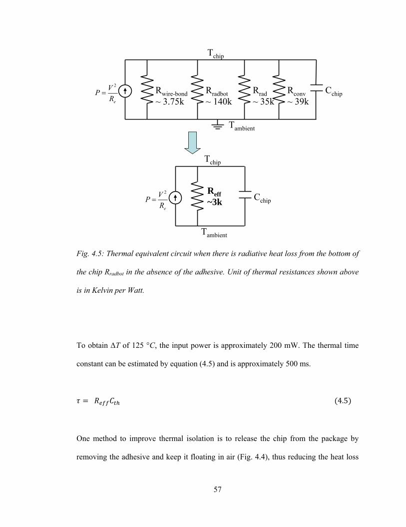
57
Fig. 4.5: Thermal equivalent circuit when there is radiative heat loss from the bottom of
the chip Rradbot in the absence of the adhesive. Unit of thermal resistances shown above
is in Kelvin per Watt.
To obtain ΔT of 125 °C, the input power is approximately 200 mW. The thermal time
constant can be estimated by equation (4.5) and is approximately 500 ms.
4.5
One method to improve thermal isolation is to release the chip from the package by
removing the adhesive and keep it floating in air (Fig. 4.4), thus reducing the heat loss
Rradbot~ 140k
CchipRrad~ 35k
Rwire-bond~ 3.75keR
VP2
=
Tchip
Tambient
Rconv~ 39k
eRVP
2
= CchipReff~3k
Tchip
Tambient
58
from the substrate to the package. The chip, in this case, is supported from the top by
six wire bonds. The equivalent thermal circuit for the released device is shown in Fig.
4.5, and the total effective thermal isolation is estimated to be approximately 3000
K/W—an improvement by a factor of five.
This method of improving thermal resistance is effective but not robust and may lead to
packaging problems. Furthermore, since the heat transfer from the heater to the
resonator takes place in the device layer, the device layer gets heated which leads to
unwanted heating up of the entire chip because of the lack of thermal isolation between
the device layer and the substrate. The thermal mass of a typical resonator chip is
approximately 1200 times larger than that of a single DETF, and hence, heating of the
entire chip leads to longer thermal time constant and more heat loss resulting in
increased input power.
4.2.2 Heating Resonator Alone With Local Thermal Isolation
Therefore, it is desired to have an alternative technique to increase the heating
efficiency by heating only the resonator and simultaneously providing large thermal
isolation between the resonator and its immediate vicinity in the device layer. This calls
for a local heat delivery and thermal-isolation mechanism. This can be achieved by
designing a resonator coupled with an in-built heater and restricting the heat loss to the
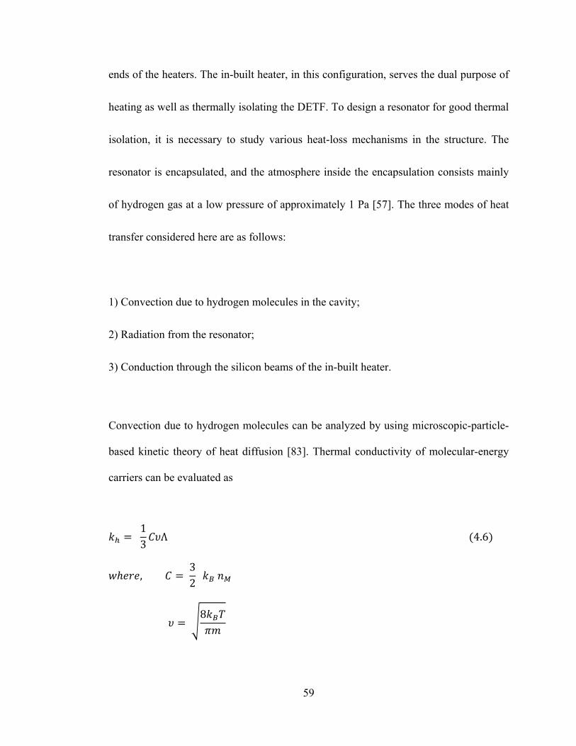
59
ends of the heaters. The in-built heater, in this configuration, serves the dual purpose of
heating as well as thermally isolating the DETF. To design a resonator for good thermal
isolation, it is necessary to study various heat-loss mechanisms in the structure. The
resonator is encapsulated, and the atmosphere inside the encapsulation consists mainly
of hydrogen gas at a low pressure of approximately 1 Pa [57]. The three modes of heat
transfer considered here are as follows:
1) Convection due to hydrogen molecules in the cavity;
2) Radiation from the resonator;
3) Conduction through the silicon beams of the in-built heater.
Convection due to hydrogen molecules can be analyzed by using microscopic-particle-
based kinetic theory of heat diffusion [83]. Thermal conductivity of molecular-energy
carriers can be evaluated as
13 Λ 4.6
, 32
8
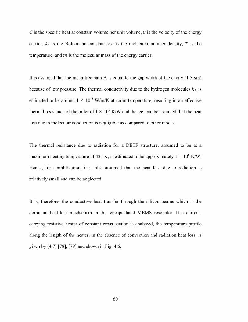
60
C is the specific heat at constant volume per unit volume, is the velocity of the energy
carrier, kB is the Boltzmann constant, nM is the molecular number density, is the
temperature, and is the molecular mass of the energy carrier.
It is assumed that the mean free path Λ is equal to the gap width of the cavity (1.5 μm)
because of low pressure. The thermal conductivity due to the hydrogen molecules is
estimated to be around 1 × 10⁻⁶ W/m/K at room temperature, resulting in an effective
thermal resistance of the order of 1 × 10⁷ K/W and, hence, can be assumed that the heat
loss due to molecular conduction is negligible as compared to other modes.
The thermal resistance due to radiation for a DETF structure, assumed to be at a
maximum heating temperature of 425 K, is estimated to be approximately 1 × 10⁶ K/W.
Hence, for simplification, it is also assumed that the heat loss due to radiation is
relatively small and can be neglected.
It is, therefore, the conductive heat transfer through the silicon beams which is the
dominant heat-loss mechanism in this encapsulated MEMS resonator. If a current-
carrying resistive heater of constant cross section is analyzed, the temperature profile
along the length of the heater, in the absence of convection and radiation heat loss, is
given by (4.7) [78], [79] and shown in Fig. 4.6.
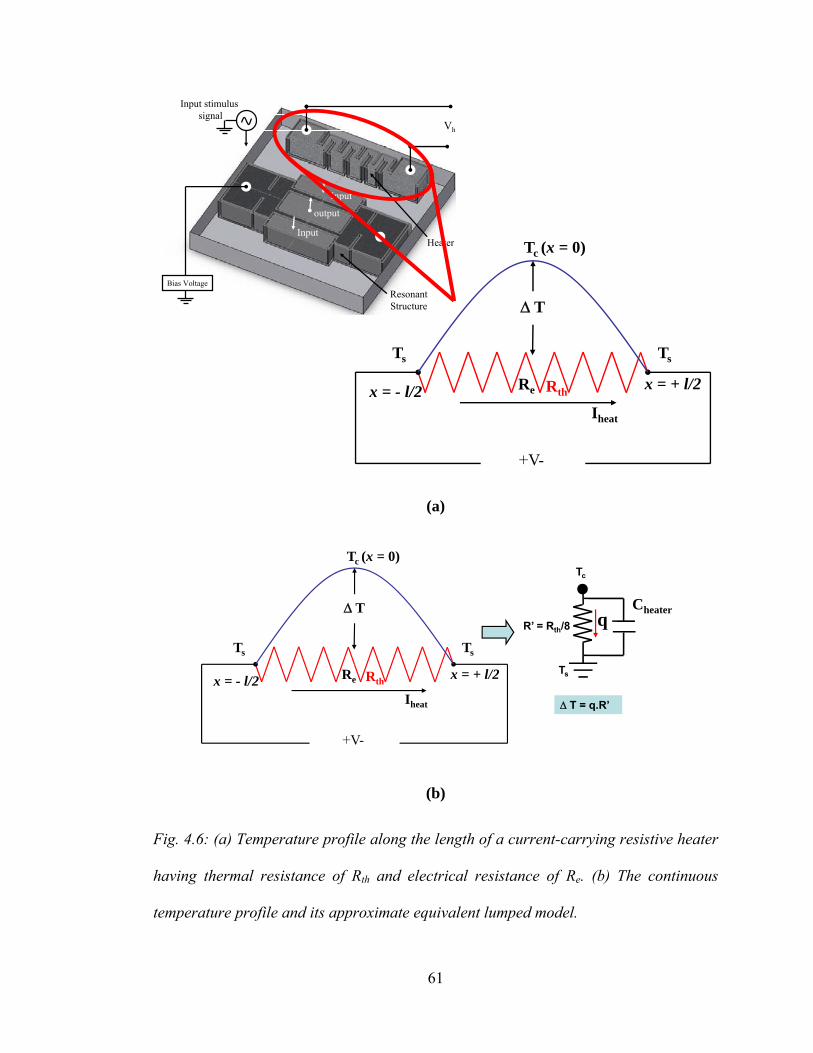
61
(a)
(b)
Fig. 4.6: (a) Temperature profile along the length of a current-carrying resistive heater
having thermal resistance of Rth and electrical resistance of Re. (b) The continuous
temperature profile and its approximate equivalent lumped model.
+V-
Iheat
Δ T
TsTs
Rth
Tc (x = 0)
x = - l/2 x = + l/2Re
output
Input stimulussignal
Vh
Bias Voltage
Input
Input
Resonant Structure
Heater
+V-
Iheat
Δ T
TsTs
Rth
Tc (x = 0)
x = - l/2 x = + l/2Re
Δ T = q.R’
qR’ = Rth/8
Tc
Ts
Cheater
62
Fig. 4.7: Resonator design with local thermal isolation. The heater is in-built to the
DETF such that the resonant structure is attached at the center of the heater. The entire
structure is released except at the four anchors.
8 1 4
4.7
where x varies from −l/2 to +l/2, and Ts is the end surface temperature of the heater
(Fig. 4.6). The maximum temperature occurs at the center of the heater (at x = 0) and is
given by
Anchor
Anchor
AnchorAnchor
Resonator Beams 220x8 microns
In-built Resistive Heater 2300x5 microns
In-built Heater
Anchor
Anchor Anchor
Anchor
Resonator Beams 220x8 microns
In-built Resistive Heater 2300x5 microns
Mechanically Coupled with DETF structure
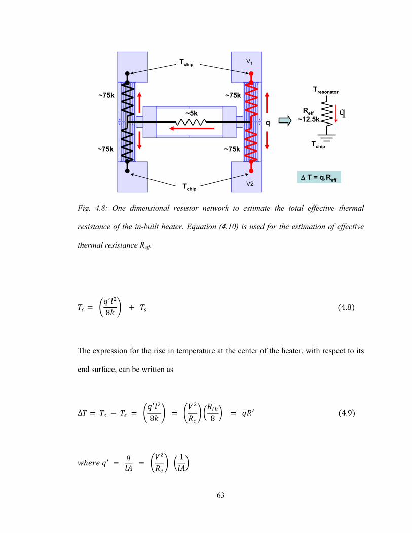
63
Fig. 4.8: One dimensional resistor network to estimate the total effective thermal
resistance of the in-built heater. Equation (4.10) is used for the estimation of effective
thermal resistance Reff.
8 4.8
The expression for the rise in temperature at the center of the heater, with respect to its
end surface, can be written as
Δ 8 8 4.9
1
Δ T = q.Reff
~75k
qReff
Tresonator
Tchip
~12.5k
~75k
~75k
~75k
~5kq
Tchip
Tchip V1
V2
64
From the equation (4.9), we can establish an equivalence between a current carrying
beam having thermal resistance of Rth and heat generation of q with a lumped model
having thermal resistance of R’ and heat flow of q for the same rise in temperature,
where R’ is eight times smaller than Rth. This suggests that the heating efficiency can be
maximized if the resonator is attached at the center of the heater and that, in order to
achieve the maximum temperature rise at the center of the heater for a given input
power, the thermal resistance of the heater should be as large as possible.
However, the micro-ovenized resonator design is suspended from both ends by in-built
resistors (Fig. 4.7 and 4.8), so the expression for the temperature of the resonator due to
heating power applied to one end of the resonator must take into account the heat loss
through the other end of the resonator. Using the equivalent thermal resistance from
equation (4.9), we can estimate the resonator temperature by considering the second
resistor in parallel with the heater resistor (Fig. 4.8). In this case, an approximate
expression for the rise in temperature at the center of the heater, with respect to its end
surface, can be written as
Δ ~ 1
1/8 1
/4 12 4.10
65
From the equation (4.10), for a resonator with a heating resistor with internal heat
generation of q at one end and an insulating resistor with no heat generation at the other
end, both having thermal resistance of Rth, we can establish an equivalent lumped
element model with a thermal resistance of Reff and heat flow of q for the same rise in
temperature, where Reff is 12 times smaller than Rth. This relationship allows us to easily
predict the resonator temperature for a given heating power, although the prediction is
not exact because the temperature distribution on the heater is modified by the heat flow
across the resonator.
Finite-element simulations (Fig. 4.10) and measurements indicate that equation (4.10)
overestimates the resonator temperature by about 20%.
The layout of the thermally isolated DETF with two in-built heaters is shown in Figs.
4.7 and 4.8. The cross section of each heater beam is 5 by 20 μm, and its total length is
approximately 2300 μm. The resonator is attached at the center of the heater for
maximum heating. The entire structure is released except at the four anchors which act
as mechanical supports at the bottom and provide electrical contacts at the top. The
anchors are electrically insulated by silicon dioxide (see Fig. 1(a)). The thermal
resistance of the in-built heater Rth is approximately 150 000 K/W. Fig. 4.8 shows an
equivalent lumped-capacitance model of the DETF with in-built heater. The effective
thermal resistance Reff of the micro-ovenized structure is calculated using equation
(4.10) and is evaluated to be approximately 12 500 K/W, which is significantly larger
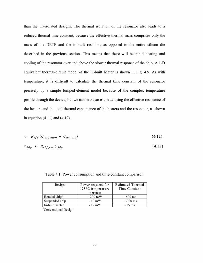
66
than the un-isolated designs. The thermal isolation of the resonator also leads to a
reduced thermal time constant, because the effective thermal mass comprises only the
mass of the DETF and the in-built resistors, as opposed to the entire silicon die
described in the previous section. This means that there will be rapid heating and
cooling of the resonator over and above the slower thermal response of the chip. A 1-D
equivalent thermal-circuit model of the in-built heater is shown in Fig. 4.9. As with
temperature, it is difficult to calculate the thermal time constant of the resonator
precisely by a simple lumped-element model because of the complex temperature
profile through the device, but we can make an estimate using the effective resistance of
the heaters and the total thermal capacitance of the heaters and the resonator, as shown
in equation (4.11) and (4.12).
τ 4.11
τ _ 4.12
Table 4.1: Power consumption and time-constant comparison
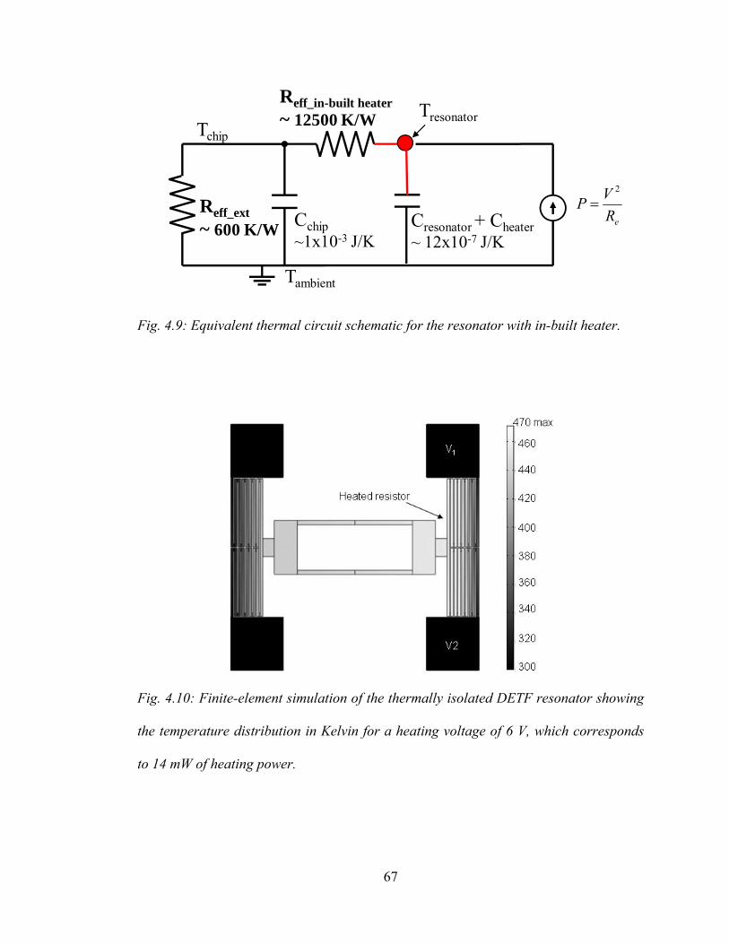
67
Fig. 4.9: Equivalent thermal circuit schematic for the resonator with in-built heater.
Fig. 4.10: Finite-element simulation of the thermally isolated DETF resonator showing
the temperature distribution in Kelvin for a heating voltage of 6 V, which corresponds
to 14 mW of heating power.
Cresonator + Cheater~ 12x10-7 J/K
Reff_ext~ 600 K/W eR
VP2
=
Tchip
Tambient
Cchip~1x10⁻³ J/K
Reff_in-built heater~ 12500 K/W Tresonator
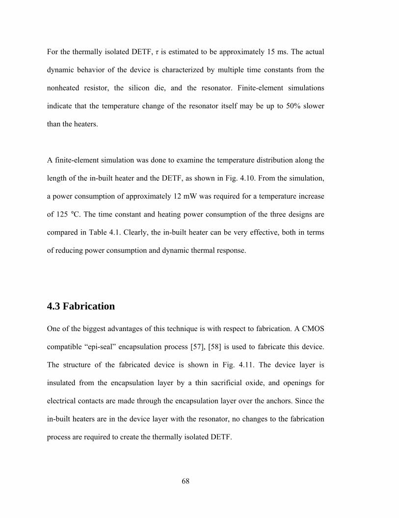
68
For the thermally isolated DETF, τ is estimated to be approximately 15 ms. The actual
dynamic behavior of the device is characterized by multiple time constants from the
nonheated resistor, the silicon die, and the resonator. Finite-element simulations
indicate that the temperature change of the resonator itself may be up to 50% slower
than the heaters.
A finite-element simulation was done to examine the temperature distribution along the
length of the in-built heater and the DETF, as shown in Fig. 4.10. From the simulation,
a power consumption of approximately 12 mW was required for a temperature increase
of 125 °C. The time constant and heating power consumption of the three designs are
compared in Table 4.1. Clearly, the in-built heater can be very effective, both in terms
of reducing power consumption and dynamic thermal response.
4.3 Fabrication
One of the biggest advantages of this technique is with respect to fabrication. A CMOS
compatible “epi-seal” encapsulation process [57], [58] is used to fabricate this device.
The structure of the fabricated device is shown in Fig. 4.11. The device layer is
insulated from the encapsulation layer by a thin sacrificial oxide, and openings for
electrical contacts are made through the encapsulation layer over the anchors. Since the
in-built heaters are in the device layer with the resonator, no changes to the fabrication
process are required to create the thermally isolated DETF.
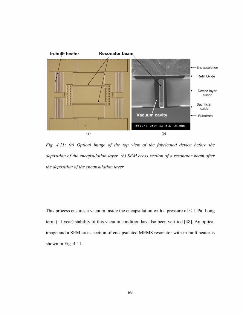
69
Fig. 4.11: (a) Optical image of the top view of the fabricated device before the
deposition of the encapsulation layer. (b) SEM cross section of a resonator beam after
the deposition of the encapsulation layer.
This process ensures a vacuum inside the encapsulation with a pressure of < 1 Pa. Long
term (~1 year) stability of this vacuum condition has also been verified [48]. An optical
image and a SEM cross section of encapsulated MEMS resonator with in-built heater is
shown in Fig. 4.11.
In-built heater Resonator beam
Encapsulation
Refill Oxide
Device layersilicon
Sacrificialoxide
Substrate
(a) (b)
Vacuum cavity
70
4.4 Experimental Results
Resonators with 1.3-MHz frequency and a mechanical Q of approximately 104 were
used for the experiment. Since silicon resonator frequency varies nearly linearly with
temperature, frequency was used as a measure of temperature for this work. However,
resonator frequency is also sensitive to bias voltage and axial strain. The bias voltage
induces capacitive nonlinearity, which causes the effective stiffness of the resonator
beam to decrease [84], reducing the resonator frequency. It is necessary to ensure that
the bias voltage is not affected by the heating current. Fig. 4.12 shows the device layer
schematic with circuit diagram of the resonator having in-built heater. Voltages V1 and
V2 are applied, such that the potential difference between them acts as a joule heating
voltage Vh across the in-built heater as shown in equation (4.13).
2
2 4.13
.
where, is the effective bias voltage experienced by the resonator and is the
heating voltage applied across the heater.
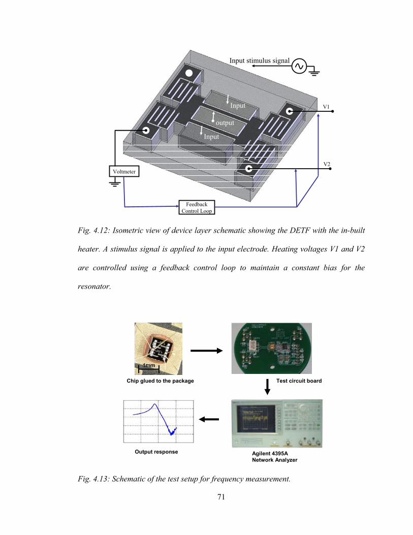
71
Fig. 4.12: Isometric view of device layer schematic showing the DETF with the in-built
heater. A stimulus signal is applied to the input electrode. Heating voltages V1 and V2
are controlled using a feedback control loop to maintain a constant bias for the
resonator.
Fig. 4.13: Schematic of the test setup for frequency measurement.
output
Input stimulus signal
V2
V1
Voltmeter
FeedbackControl Loop
Input
Input
Chip glued to the package Test circuit board
Agilent 4395ANetwork Analyzer
Output response
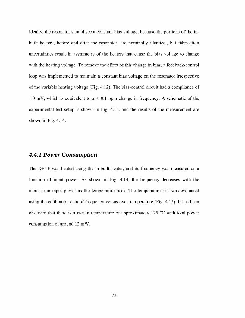
72
Ideally, the resonator should see a constant bias voltage, because the portions of the in-
built heaters, before and after the resonator, are nominally identical, but fabrication
uncertainties result in asymmetry of the heaters that cause the bias voltage to change
with the heating voltage. To remove the effect of this change in bias, a feedback-control
loop was implemented to maintain a constant bias voltage on the resonator irrespective
of the variable heating voltage (Fig. 4.12). The bias-control circuit had a compliance of
1.0 mV, which is equivalent to a < 0.1 ppm change in frequency. A schematic of the
experimental test setup is shown in Fig. 4.13, and the results of the measurement are
shown in Fig. 4.14.
4.4.1 Power Consumption
The DETF was heated using the in-built heater, and its frequency was measured as a
function of input power. As shown in Fig. 4.14, the frequency decreases with the
increase in input power as the temperature rises. The temperature rise was evaluated
using the calibration data of frequency versus oven temperature (Fig. 4.15). It has been
observed that there is a rise in temperature of approximately 125 °C with total power
consumption of around 12 mW.
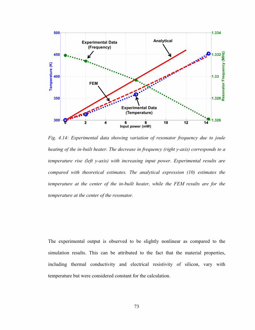
73
Fig. 4.14: Experimental data showing variation of resonator frequency due to joule
heating of the in-built heater. The decrease in frequency (right y-axis) corresponds to a
temperature rise (left y-axis) with increasing input power. Experimental results are
compared with theoretical estimates. The analytical expression (10) estimates the
temperature at the center of the in-built heater, while the FEM results are for the
temperature at the center of the resonator.
The experimental output is observed to be slightly nonlinear as compared to the
simulation results. This can be attributed to the fact that the material properties,
including thermal conductivity and electrical resistivity of silicon, vary with
temperature but were considered constant for the calculation.
0 2 4 6 8 10 12 14300
350
400
450
500
Tem
pera
ture
(K)
Input power (mW)0 2 4 6 8 10 12 14 1.326
1.328
1.33
1.332
1.334
Res
onat
or F
requ
ency
(MH
z)
Experimental Data(Frequency)
Experimental Data(Temperature)
Analytical
FEM
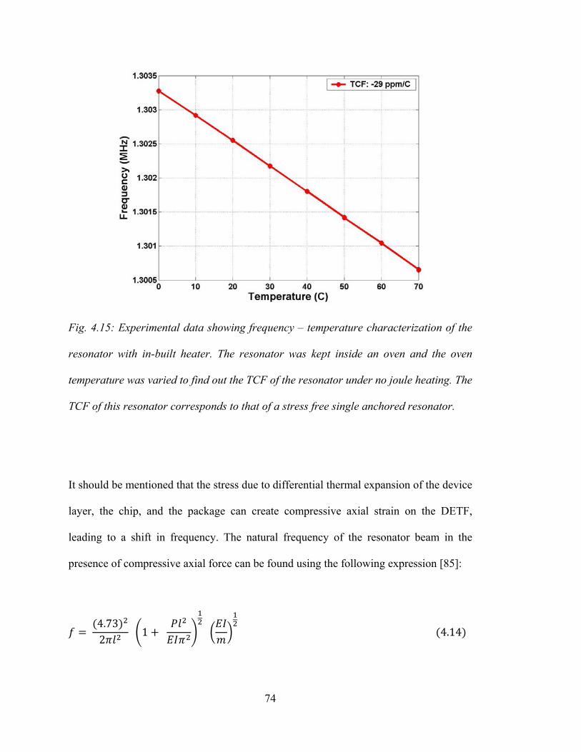
74
Fig. 4.15: Experimental data showing frequency – temperature characterization of the
resonator with in-built heater. The resonator was kept inside an oven and the oven
temperature was varied to find out the TCF of the resonator under no joule heating. The
TCF of this resonator corresponds to that of a stress free single anchored resonator.
It should be mentioned that the stress due to differential thermal expansion of the device
layer, the chip, and the package can create compressive axial strain on the DETF,
leading to a shift in frequency. The natural frequency of the resonator beam in the
presence of compressive axial force can be found using the following expression [85]:
4.732 1 4.14
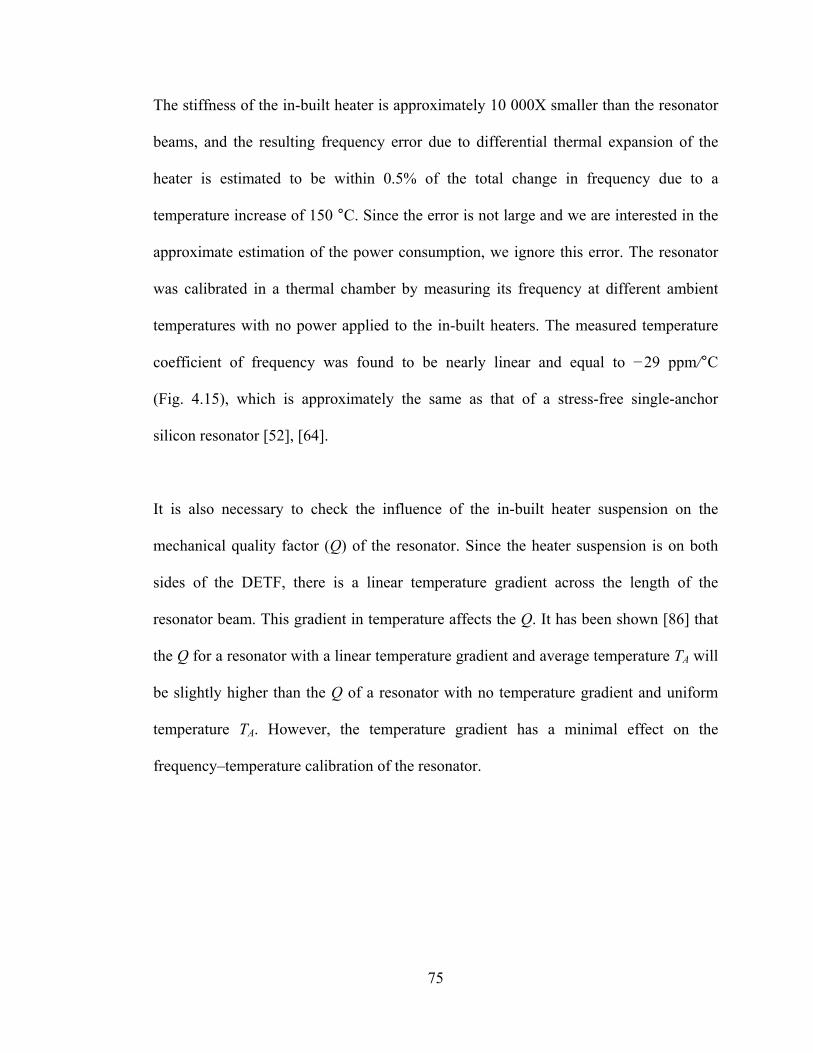
75
The stiffness of the in-built heater is approximately 10 000X smaller than the resonator
beams, and the resulting frequency error due to differential thermal expansion of the
heater is estimated to be within 0.5% of the total change in frequency due to a
temperature increase of 150 °C. Since the error is not large and we are interested in the
approximate estimation of the power consumption, we ignore this error. The resonator
was calibrated in a thermal chamber by measuring its frequency at different ambient
temperatures with no power applied to the in-built heaters. The measured temperature
coefficient of frequency was found to be nearly linear and equal to −29 ppm/°C
(Fig. 4.15), which is approximately the same as that of a stress-free single-anchor
silicon resonator [52], [64].
It is also necessary to check the influence of the in-built heater suspension on the
mechanical quality factor (Q) of the resonator. Since the heater suspension is on both
sides of the DETF, there is a linear temperature gradient across the length of the
resonator beam. This gradient in temperature affects the Q. It has been shown [86] that
the Q for a resonator with a linear temperature gradient and average temperature TA will
be slightly higher than the Q of a resonator with no temperature gradient and uniform
temperature TA. However, the temperature gradient has a minimal effect on the
frequency–temperature calibration of the resonator.
76
4.4.2 Thermal Time Constant
The thermal time constant of the micro-ovenized resonator is an important parameter
for temperature control. The thermal response was evaluated using a transient electrical-
resistance measurement. A voltage pulse was applied to the heater, which caused its
resistance to increase as it heated up. After the pulse ended, the heater resistance
decreased as it cooled. A wheatstone bridge was used to measure the change in heater
resistance during this cycle (Fig. 4.16). For the measurement, a heating pulse of 4.5 V
was used, and the voltage was maintained at 0.5 V during the cooling period in order to
observe the change in voltage during cooling.
The measured time constants of several resonators varied between 7 and 10 ms. A
typical measurement is shown in Fig. 4.16. We expect the measurement to understate
the time constant, because the measurement indicates the average temperature of the
heater, not the temperature of the resonator itself. It is to be noted that the thermal
capacitance of the DETF is approximately equal to that of an in-built heater, and so,
there is potential in further reducing the thermal time constant in future designs by
reducing the thermal mass of the resonator itself.
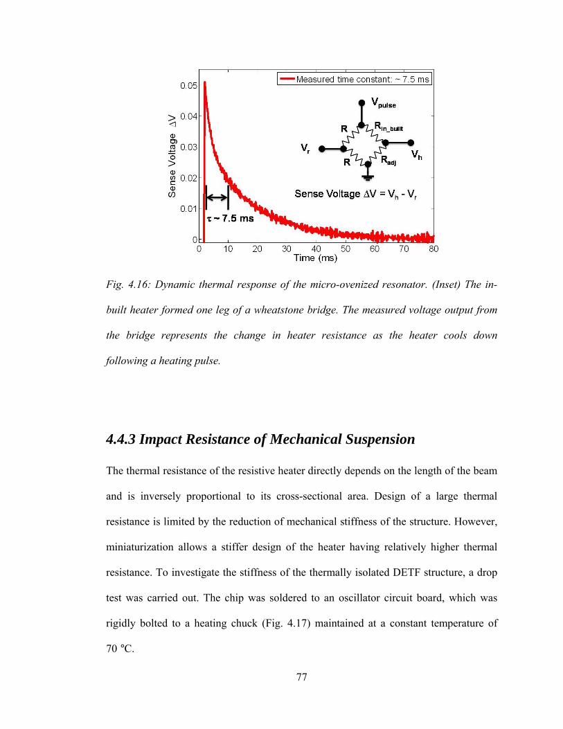
77
Fig. 4.16: Dynamic thermal response of the micro-ovenized resonator. (Inset) The in-
built heater formed one leg of a wheatstone bridge. The measured voltage output from
the bridge represents the change in heater resistance as the heater cools down
following a heating pulse.
4.4.3 Impact Resistance of Mechanical Suspension
The thermal resistance of the resistive heater directly depends on the length of the beam
and is inversely proportional to its cross-sectional area. Design of a large thermal
resistance is limited by the reduction of mechanical stiffness of the structure. However,
miniaturization allows a stiffer design of the heater having relatively higher thermal
resistance. To investigate the stiffness of the thermally isolated DETF structure, a drop
test was carried out. The chip was soldered to an oscillator circuit board, which was
rigidly bolted to a heating chuck (Fig. 4.17) maintained at a constant temperature of
70 °C.
78
Fig. 4.17: Drop test resulted in a temporary change in frequency at the time of drop.
The chuck was dropped from a height of 1.0 cm onto a rigid platform, and the response
of the resonator frequency was measured, as shown in Fig. 4.17. At the time of the
impact, the oscillator frequency changed by approximately −45 000 ppm. The resonator
immediately returned to normal operation. The change in frequency before and after the
impact is within the noise of the frequency fluctuation of the uncompensated resonator
due to small variation in the chuck temperature, as shown in Fig. 4.17. Furthermore, the
resonators survived the 5000-rpm rotation (up to 1400 g of acceleration) during the
photoresist spin-coating steps of the fabrication process. The spin duration was
approximately 1 min and was repeated six to eight times during the fabrication.
Drop at t ~ 85 sec
Temperaturefluctuation Drop
Frequency variation due totemperature fluctuation
After impact
Before impact
Chuck containingoscillator circuit
board
Base of metal chuck~ 2.5cm x 30cm x 30cm
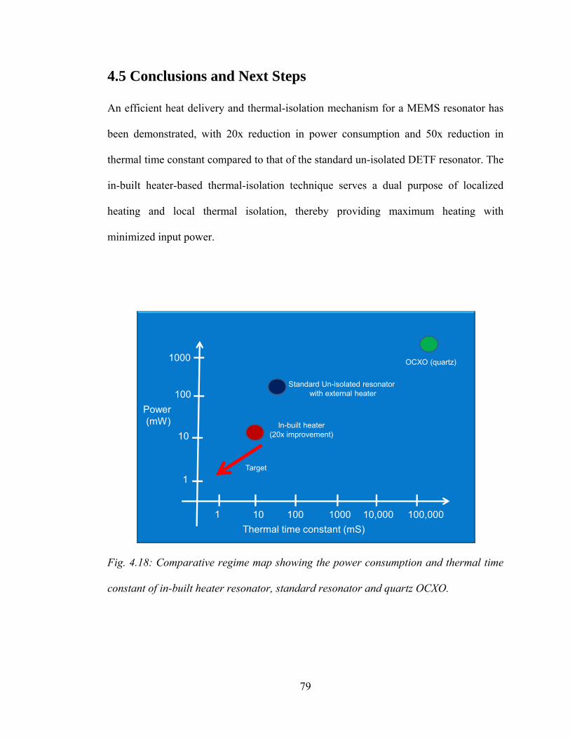
79
4.5 Conclusions and Next Steps
An efficient heat delivery and thermal-isolation mechanism for a MEMS resonator has
been demonstrated, with 20x reduction in power consumption and 50x reduction in
thermal time constant compared to that of the standard un-isolated DETF resonator. The
in-built heater-based thermal-isolation technique serves a dual purpose of localized
heating and local thermal isolation, thereby providing maximum heating with
minimized input power.
Fig. 4.18: Comparative regime map showing the power consumption and thermal time
constant of in-built heater resonator, standard resonator and quartz OCXO.
Thermal time constant (mS)
Power (mW)
10
1
100
1000
1 10 100 1000 10,000 100,000
In-built heater(20x improvement)
Standard Un-isolated resonator with external heater
OCXO (quartz)
Target
80
At the same time, the device has high impact resistance because of its miniature design.
Compared to the commercially used quartz crystals (1–10 W and around 30 min warm-
up time), this technique has demonstrated orders of- magnitude improvement in power
dissipation and dynamic thermal response with a potential for further improvement. A
comparative regime map is shown in Fig. 4.18. Furthermore, this method is simple
enough to implement it into any existing MEMS fabrication process. The described
design of micro-oven is highly suitable for temperature stabilization of
micromechanical resonators and for very precise control of frequency (< 1.0 ppm) over
a temperature span of 125°C.
It is possible to further reduce the power consumption by increasing the thermal
resistance of the in-built heater. The thermal resistance of a single-crystal silicon heater,
with known thermal conductivity, is dependent on the length and the cross-section of
the heater geometry as given below
4.15
The thermal resistance of the heater can be increased either by increasing its length or
by decreasing its cross-section area. The cross-section area is limited by the fabrication
constraints and hence difficult to reduce beyond a certain point. The only parameter to
play with, is the length of the heater.
81
However, it is difficult to increase the length of the heater structure arbitrarily as it is
related to the stiffness of the structure as given below
1
4.16
The stiffness of the structure should be large enough to keep the device mechanically
robust and reliable.
From equations (4.15) and (4.16), it can be interpreted that it is difficult to increase the
thermal resistance of the heater without first studying the mechanical stiffness of the
device and its effect on the performance of the device. In other words, the DETF
resonator needs to be not only thermally isolated but also mechanically isolated.

82
83
Chapter 5
Mechanical Isolation of MEMS Resonator
This chapter presents an investigative study of mechanical robustness or isolation of the
electrostatically coupled encapsulated silicon DETF micromechanical resonator. This
study of mechanical isolation of the resonator is necessary to understand the limit of the
thermal isolation. The external vibration and acceleration from the environment affects
the performance of the resonator. The chapter describes the acceleration sensitivity and
the resulting vibration-induced phase noise of a standard as well as thermally isolated
resonator. The thermally isolated resonator described in the previous chapter is renamed
as a spring mounted resonator in this chapter for better clarity. External vibrations can
produce phase noise in micromechanical resonators by generating time-varying stress in
the resonant beams. However, the spring mounted design can reduce this induced axial
stress. Measurements and simulations show that the acceleration sensitivity and the
vibration-induced phase noise of this device can be reduced 1000x smaller than that of
the previously published silicon micromechanical resonator and 10x smaller than the
commercially used high end SC (stress compensated)-cut quartz resonator. The chapter
also describes the analysis of vibration isolation. The vibration isolation discussed at the
end of the chapter is different from the acceleration dependent vibration-induced phase
noise. The vibration isolation primarily focuses on the magnification of the effect of the
external vibration due to the lateral resonance of the entire DETF resonator structure.
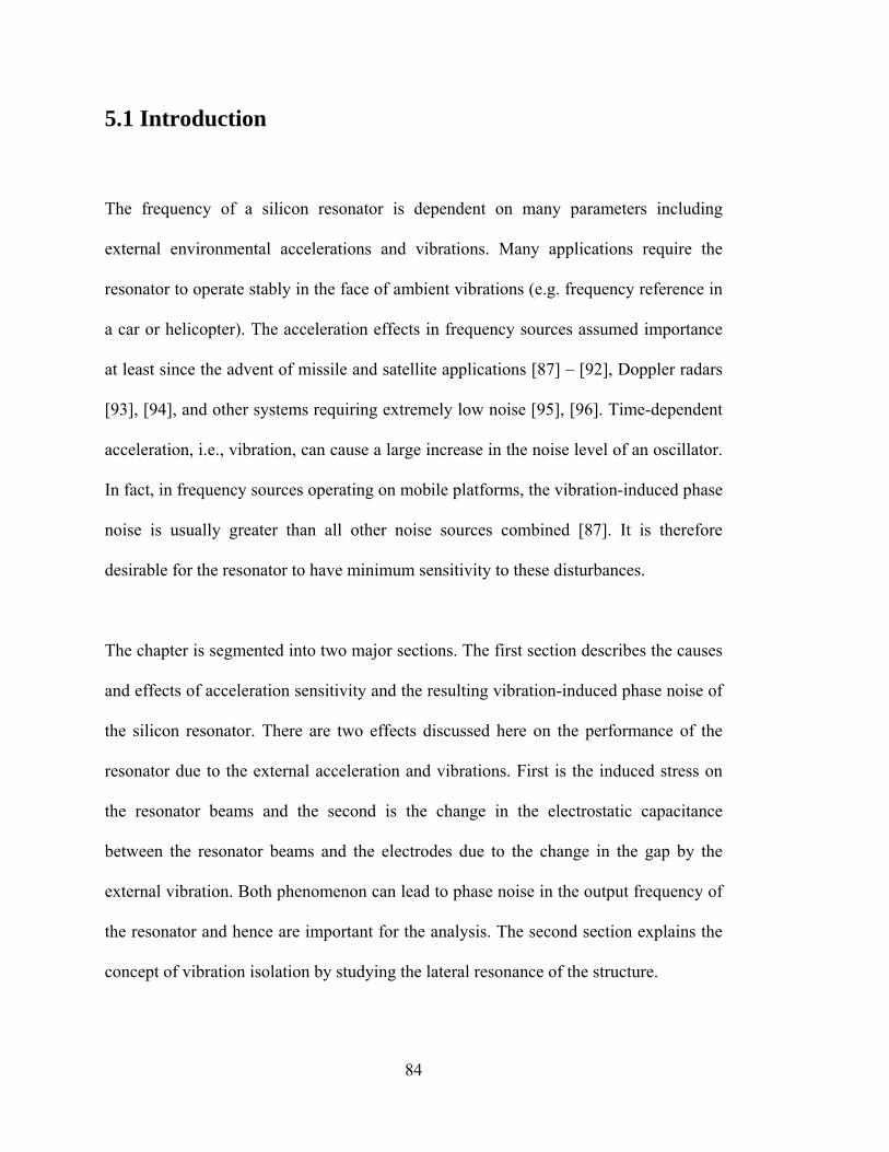
84
5.1 Introduction
The frequency of a silicon resonator is dependent on many parameters including
external environmental accelerations and vibrations. Many applications require the
resonator to operate stably in the face of ambient vibrations (e.g. frequency reference in
a car or helicopter). The acceleration effects in frequency sources assumed importance
at least since the advent of missile and satellite applications [87] – [92], Doppler radars
[93], [94], and other systems requiring extremely low noise [95], [96]. Time-dependent
acceleration, i.e., vibration, can cause a large increase in the noise level of an oscillator.
In fact, in frequency sources operating on mobile platforms, the vibration-induced phase
noise is usually greater than all other noise sources combined [87]. It is therefore
desirable for the resonator to have minimum sensitivity to these disturbances.
The chapter is segmented into two major sections. The first section describes the causes
and effects of acceleration sensitivity and the resulting vibration-induced phase noise of
the silicon resonator. There are two effects discussed here on the performance of the
resonator due to the external acceleration and vibrations. First is the induced stress on
the resonator beams and the second is the change in the electrostatic capacitance
between the resonator beams and the electrodes due to the change in the gap by the
external vibration. Both phenomenon can lead to phase noise in the output frequency of
the resonator and hence are important for the analysis. The second section explains the
concept of vibration isolation by studying the lateral resonance of the structure.
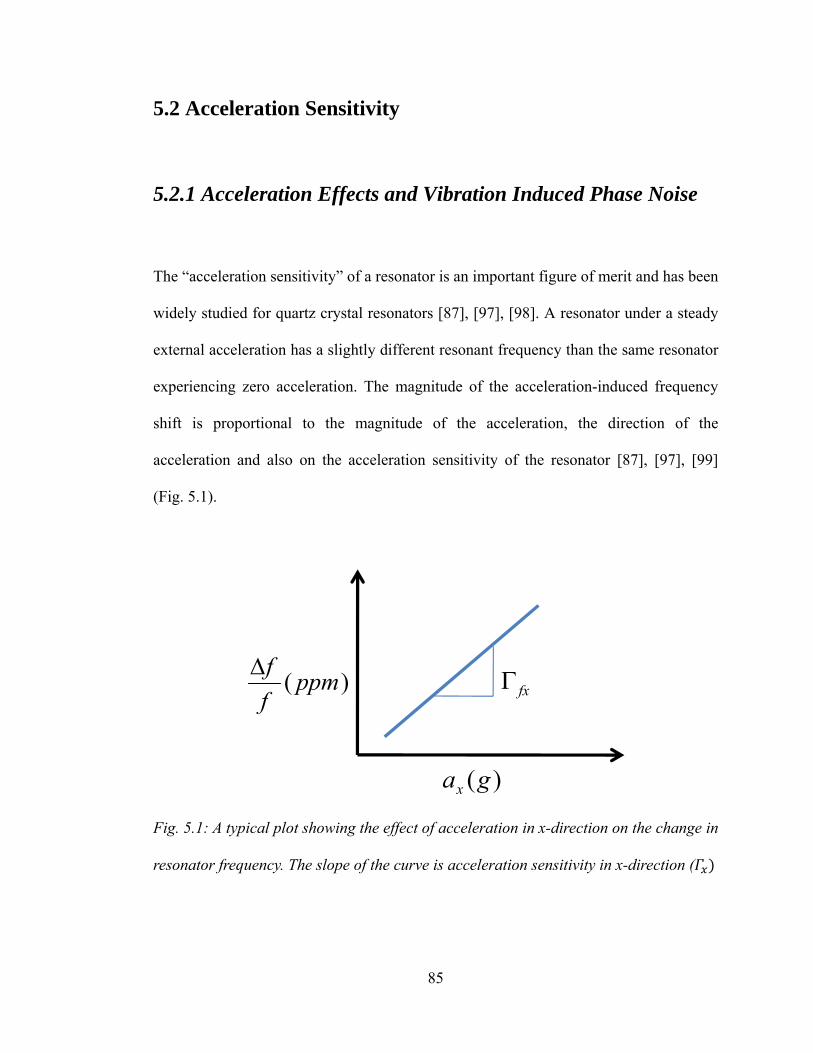
85
5.2 Acceleration Sensitivity
5.2.1 Acceleration Effects and Vibration Induced Phase Noise
The “acceleration sensitivity” of a resonator is an important figure of merit and has been
widely studied for quartz crystal resonators [87], [97], [98]. A resonator under a steady
external acceleration has a slightly different resonant frequency than the same resonator
experiencing zero acceleration. The magnitude of the acceleration-induced frequency
shift is proportional to the magnitude of the acceleration, the direction of the
acceleration and also on the acceleration sensitivity of the resonator [87], [97], [99]
(Fig. 5.1).
Fig. 5.1: A typical plot showing the effect of acceleration in x-direction on the change in
resonator frequency. The slope of the curve is acceleration sensitivity in x-direction (
)(gax
)( ppmffΔ
fxΓ
86
Therefore, the frequency during acceleration can be written as
1 . 1 Γ Γ Γ 5.1
where is frequency of the resonator experiencing acceleration , is the frequency
with no acceleration (often referred to as the “carrier frequency”), and is the
acceleration sensitivity. The normalized frequency shift due to acceleration is given by
equation (5.2).
Δ. Γ Γ Γ 5.2
Time-dependent acceleration (Fig. 5.2 and Fig. 5.3), i.e. vibration, can cause vibration
induced phase noise. The time dependent frequency variation of the resonator due to a
sinusoidal external vibration at can be determined by
1 . 1 . 2 5.3
where is the peak acceleration in g, is the frequency in Hz, and is time in
seconds. Using (5.2), this can be rewritten as shown in equation (5.4)
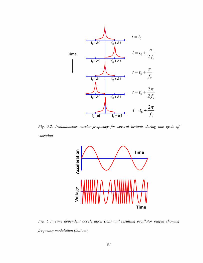
87
Fig. 5.2: Instantaneous carrier frequency for several instants during one cycle of
vibration.
Fig. 5.3: Time dependent acceleration (top) and resulting oscillator output showing
frequency modulation (bottom).
Time
f0 ‐ ∆f f0 + ∆ f 0tt =
f0 ‐ ∆f f0 + ∆ f
f0 ‐ ∆f f0 + ∆ f
f0 ‐ ∆f f0 + ∆ f
f0 ‐ ∆f f0 + ∆ f
vftt
20π
+=
vftt π+= 0
vftt
23
0π
+=
vftt π2
0 +=
Acceleration Time
Time
Volta
ge
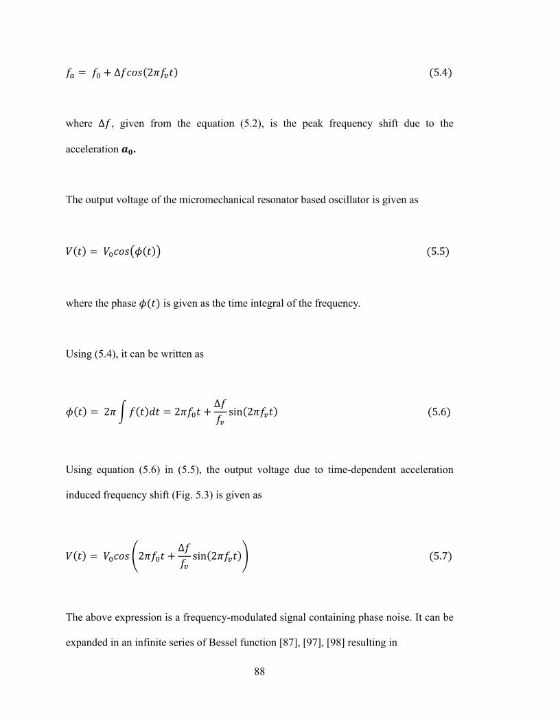
88
Δ 2 5.4
where Δ , given from the equation (5.2), is the peak frequency shift due to the
acceleration .
The output voltage of the micromechanical resonator based oscillator is given as
5.5
where the phase is given as the time integral of the frequency.
Using (5.4), it can be written as
2 2Δ
sin 2 5.6
Using equation (5.6) in (5.5), the output voltage due to time-dependent acceleration
induced frequency shift (Fig. 5.3) is given as
2Δ
sin 2 5.7
The above expression is a frequency-modulated signal containing phase noise. It can be
expanded in an infinite series of Bessel function [87], [97], [98] resulting in
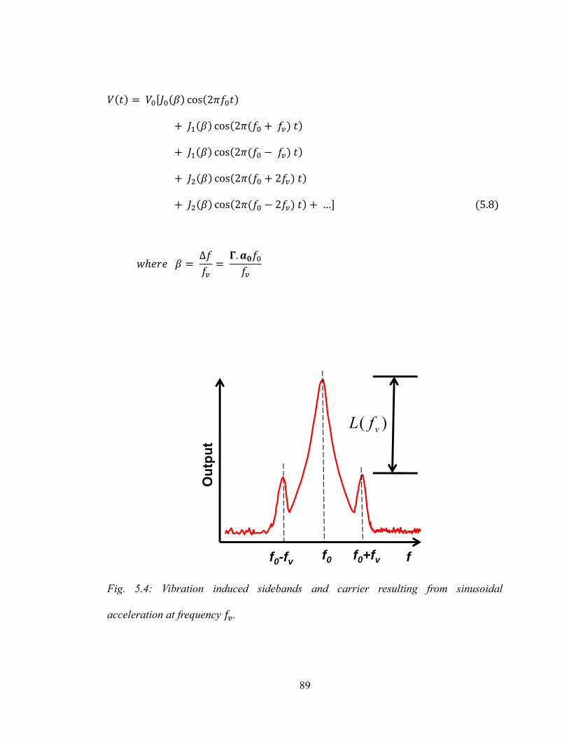
89
cos 2
cos 2
cos 2
cos 2 2
cos 2 2 … 5.8
∆
.
Fig. 5.4: Vibration induced sidebands and carrier resulting from sinusoidal
acceleration at frequency .
f0 f0+fvf0-fv f
Out
put
)( vfL
90
The parameter in equation (5.8) is known as the modulation index [87], [97]. The
first term in equation (5.8) represents the original signal at carrier frequency. The other
terms are vibration-induced sidebands at frequencies , , 2 ,
2 , etc. Most of the power is in the carrier, a small amount is in the first spectral line
pair, and the higher order spectral lines are negligible. For a small modulation index,
0.1, the relative strength of vibration induced phase noise with respect to the
carrier in the first spectral line pair is shown in Fig. 5.4 and is given by [87], [97],
[99], [100]
20 .2 5.9
5.2.2 Model for Axial Stress in the Resonator Beams
The principal mechanism that causes the acceleration sensitivity is the axial stress
experienced by the resonator beams. This section describes an analysis of the axial
stress in the beams of the resonator. The axial stress in the spring mounted double ended
tuning fork (DETF) type resonator is compared with that of our previously published
basic single anchored DETF resonator as shown in Fig. 5.5.
There are two modes of vibration associated with the resonator discussed in this chapter.
One is the tuning fork vibration mode which is stimulated by the input electrode and
another one is the lateral mode vibration which is stimulated by the external vibration.
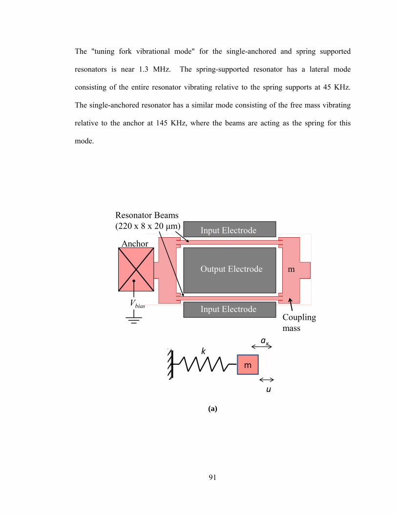
91
The "tuning fork vibrational mode" for the single-anchored and spring supported
resonators is near 1.3 MHz. The spring-supported resonator has a lateral mode
consisting of the entire resonator vibrating relative to the spring supports at 45 KHz.
The single-anchored resonator has a similar mode consisting of the free mass vibrating
relative to the anchor at 145 KHz, where the beams are acting as the spring for this
mode.
(a)
m
axk
u
Input ElectrodeVbias
AnchorInput Electrode
Output Electrode
Resonator Beams(220 x 8 x 20 μm)
m
Coupling mass
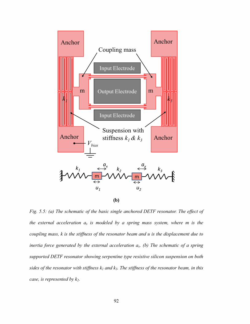
92
(b)
Fig. 5.5: (a) The schematic of the basic single anchored DETF resonator. The effect of
the external acceleration ax is modeled by a spring mass system, where m is the
coupling mass, k is the stiffness of the resonator beam and u is the displacement due to
inertia force generated by the external acceleration ax. (b) The schematic of a spring
supported DETF resonator showing serpentine type resistive silicon suspension on both
sides of the resonator with stiffness k1 and k3. The stiffness of the resonator beam, in this
case, is represented by k2.
m
Input Electrode
Output Electrode
Input Electrode
m
Anchor
Anchor Anchor
Anchor
k1 k3
Suspension withstiffness k1 & k3
Coupling mass
Vbias
m
axk1
u1
mk2 k3
u2
ax
93
The external vibration or the acceleration causes an axial force on the resonator beam.
The dependence of resonator frequency on axial load P is given by [85]
2 1 , 4.73 5.10
where is a dimensionless parameter which is a function of the boundary conditions
applied to the beam and is equal to 4.73 for a free-free or clamped-clamped beam, is
the length of the beam, is the modulus of elasticity, I is the area moment of inertia of
the beam about neutral axis, and m is the mass per unit length of the beam.
The axial load experienced by the resonator beam can be estimated with the help of a
static analysis using a lumped spring mass model as shown in Fig. 5.5. The axial load
due to external acceleration ax for the basic DETF structure is given by
5.11
where m is the lumped mass (coupling mass + half the mass of the beams) and k is
the stiffness of the resonator beam. The mass of the beam is included in the calculation
of the lumped mass to account for the effect of the distributed mass of the beam on the
axial load. From the equations (5.10) and (5.11), the change in frequency Δ is
estimated to be approximately 0.01 Hz for 1g of acceleration resulting in the
acceleration sensitivity Γ of approximately 6.5 ppb/g from the equation (5.2).
94
For the spring supported DETF structure, the axial load experienced by the resonator
beam is given by
5.12
where is the stiffness of the resonator beam and are the stiffnesses of the
mechanical suspension on both sides of the resonator. As can be seen from (5.12), if
is equal to , i.e., the left and right support are equally stiff, then the axial load
experienced by the resonator beam tends to zero. It should be mentioned that this
lumped model is effective only when , and it can be assumed that the inertia
effect of the distributed mass of the resonator beam are negligible. In case of
, , the mass of the resonator beam needs to be accounted for and should not be
neglected. For this design 10,000 . Since the design of the spring mounted
DETF resonator is symmetric (Fig. 5.5(b)), it can be assumed that , resulting in
an acceleration insensitive resonator. However, if we account for the variations in the
process parameters of our fabrication process, the difference in can be as
high as 5% resulting in the acceleration sensitivity of upto 0.1ppb/g. For a simplified
theoretical analysis here, we will stick to the assumption of a symmetric design and
ignore the error due to fabrication.
The above analysis is based on a simple lumped model and does not capture the effect
of the distributed mass of the resonator beams. To investigate this, a finite element
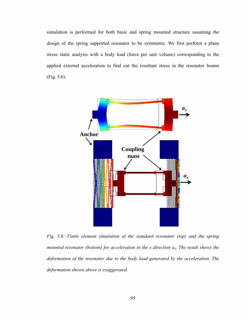
95
simulation is performed for both basic and spring mounted structure assuming the
design of the spring supported resonator to be symmetric. We first perform a plane
stress static analysis with a body load (force per unit volume) corresponding to the
applied external acceleration to find out the resultant stress in the resonator beams
(Fig. 5.6).
Fig. 5.6: Finite element simulation of the standard resonator (top) and the spring
mounted resonator (bottom) for acceleration in the x direction ax. The result shows the
deformation of the resonator due to the body load generated by the acceleration. The
deformation shown above is exaggerated.
Anchor
Coupling mass
ax
ax
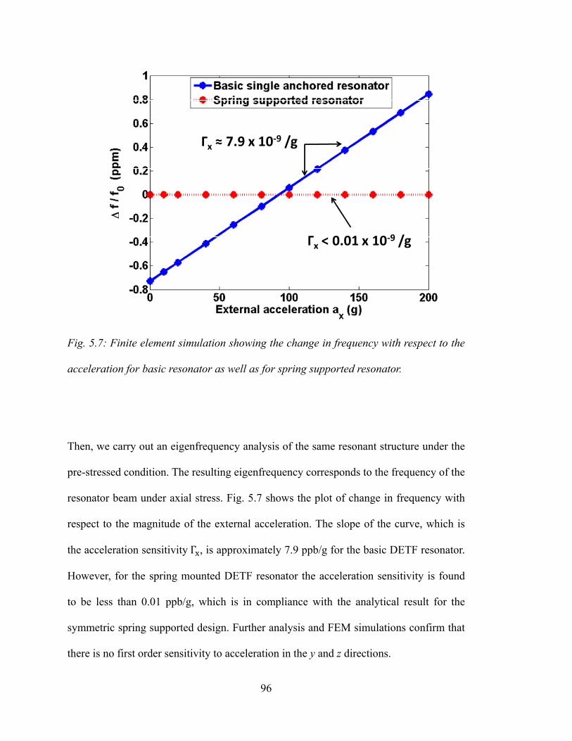
96
Fig. 5.7: Finite element simulation showing the change in frequency with respect to the
acceleration for basic resonator as well as for spring supported resonator.
Then, we carry out an eigenfrequency analysis of the same resonant structure under the
pre-stressed condition. The resulting eigenfrequency corresponds to the frequency of the
resonator beam under axial stress. Fig. 5.7 shows the plot of change in frequency with
respect to the magnitude of the external acceleration. The slope of the curve, which is
the acceleration sensitivity Γ , is approximately 7.9 ppb/g for the basic DETF resonator.
However, for the spring mounted DETF resonator the acceleration sensitivity is found
to be less than 0.01 ppb/g, which is in compliance with the analytical result for the
symmetric spring supported design. Further analysis and FEM simulations confirm that
there is no first order sensitivity to acceleration in the y and z directions.
Гx ≈ 7.9 x 10‐9 /g
Гx < 0.01 x 10‐9 /g
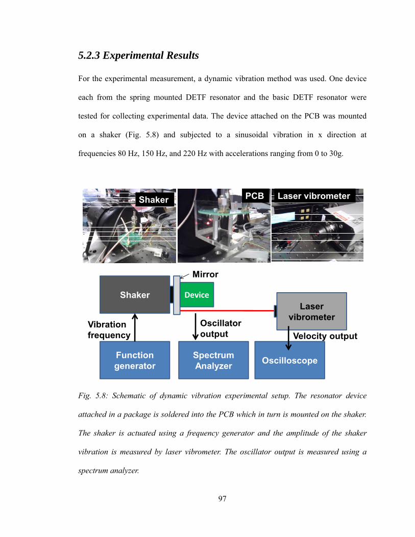
97
5.2.3 Experimental Results
For the experimental measurement, a dynamic vibration method was used. One device
each from the spring mounted DETF resonator and the basic DETF resonator were
tested for collecting experimental data. The device attached on the PCB was mounted
on a shaker (Fig. 5.8) and subjected to a sinusoidal vibration in x direction at
frequencies 80 Hz, 150 Hz, and 220 Hz with accelerations ranging from 0 to 30g.
Fig. 5.8: Schematic of dynamic vibration experimental setup. The resonator device
attached in a package is soldered into the PCB which in turn is mounted on the shaker.
The shaker is actuated using a frequency generator and the amplitude of the shaker
vibration is measured by laser vibrometer. The oscillator output is measured using a
spectrum analyzer.
Laser vibrometer
Shaker Device
Function generator
Spectrum Analyzer Oscilloscope
Vibration frequency
Oscillator output
Mirror
Velocity output
Shaker PCB Laser vibrometer
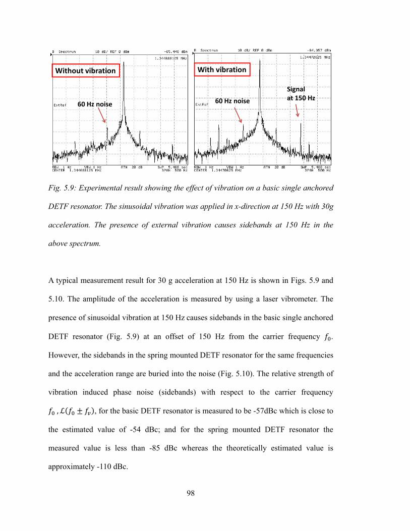
98
Fig. 5.9: Experimental result showing the effect of vibration on a basic single anchored
DETF resonator. The sinusoidal vibration was applied in x-direction at 150 Hz with 30g
acceleration. The presence of external vibration causes sidebands at 150 Hz in the
above spectrum.
A typical measurement result for 30 g acceleration at 150 Hz is shown in Figs. 5.9 and
5.10. The amplitude of the acceleration is measured by using a laser vibrometer. The
presence of sinusoidal vibration at 150 Hz causes sidebands in the basic single anchored
DETF resonator (Fig. 5.9) at an offset of 150 Hz from the carrier frequency .
However, the sidebands in the spring mounted DETF resonator for the same frequencies
and the acceleration range are buried into the noise (Fig. 5.10). The relative strength of
vibration induced phase noise (sidebands) with respect to the carrier frequency
, , for the basic DETF resonator is measured to be -57dBc which is close to
the estimated value of -54 dBc; and for the spring mounted DETF resonator the
measured value is less than -85 dBc whereas the theoretically estimated value is
approximately -110 dBc.
With vibrationWithout vibration
Signalat 150 Hz
60 Hz noise 60 Hz noise
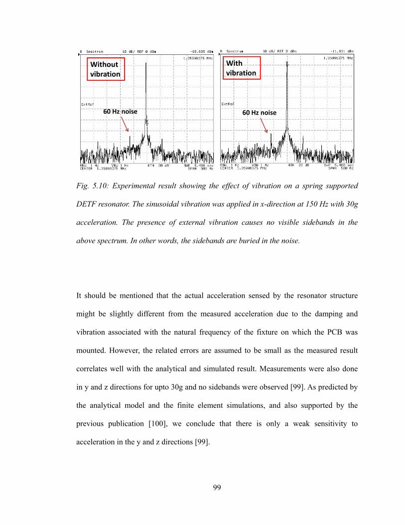
99
Fig. 5.10: Experimental result showing the effect of vibration on a spring supported
DETF resonator. The sinusoidal vibration was applied in x-direction at 150 Hz with 30g
acceleration. The presence of external vibration causes no visible sidebands in the
above spectrum. In other words, the sidebands are buried in the noise.
It should be mentioned that the actual acceleration sensed by the resonator structure
might be slightly different from the measured acceleration due to the damping and
vibration associated with the natural frequency of the fixture on which the PCB was
mounted. However, the related errors are assumed to be small as the measured result
correlates well with the analytical and simulated result. Measurements were also done
in y and z directions for upto 30g and no sidebands were observed [99]. As predicted by
the analytical model and the finite element simulations, and also supported by the
previous publication [100], we conclude that there is only a weak sensitivity to
acceleration in the y and z directions [99].
With vibration
Without vibration
60 Hz noise 60 Hz noise
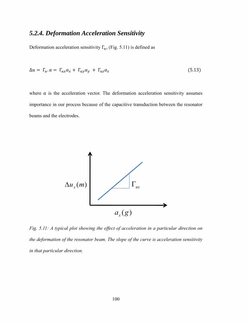
100
5.2.4. Deformation Acceleration Sensitivity
Deformation acceleration sensitivity Γ , (Fig. 5.11) is defined as
Δ Γ . Γ Γ Γ 5.13
where is the acceleration vector. The deformation acceleration sensitivity assumes
importance in our process because of the capacitive transduction between the resonator
beams and the electrodes.
Fig. 5.11: A typical plot showing the effect of acceleration in a particular direction on
the deformation of the resonator beam. The slope of the curve is acceleration sensitivity
in that particular direction.
)(gax
)(muxΔ uxΓ
101
Any substantial deformation of the resonator structure due to external acceleration leads
to change in capacitive force which in turn can lead to either snapping of the resonator
beams to the electrodes or change in resonator frequency. In this section we will analyze
both effects.
A voltage controlled parallel-plate electrostatic capacitor exhibits an important behavior
called pull-in. In order to explain it, we consider the stability of the equilibrium that
must exist between the electrostatic force pulling the plates toward each other and the
spring force of the parallel plate acting as a restoring force. Stability analysis involves
perturbing the position slightly and asking whether or not the net force tends to return to
the equilibrium position.
The capacitive force at voltage V and gap g, using a sign convention that assigns a
positive sign for forces that increases the gap, is [101]
2 5.14
where is the gap at zero volts and zero spring extension, is the permittivity of the
material between the gap (vacuum in this case), is the spring constant of the parallel
plate. At a point of equilibrium, is zero. If we now ask how varies with a
small perturbation of the gap to g + δg , we can write
102
5.15
If is positive for positive , then g is an unstable equilibrium point, because a
small increase creates a force tending to increase it further. If is negative, then
g is a stable equilibrium point.
We can evaluate using
5.16
In order for g to be stable equilibrium, the expression in parenthesis must be negative,
which means that
5.17
Clearly, at equilibrium (pull-in voltage) there are two equations that must be satisfied:
the original requirement that F = 0, and the new requirement that
5.18
103
From equations (5.14) and (5.18), it can be shown that the pull-in occurs at
gPI23 g 5.19
This means, if the deflection of the resonator beam is more than one-third of the original
gap (g , then the beam will snap to the electrode, leading to the failure of the device.
The above analysis of pull-in gap will be the basis for the design of the resonator
structure for the deformation acceleration sensitivity (Γ ). For example, for a gap size of
1.5μm between the resonator beam and the electrodes, any force due to external
acceleration causing beam deformation more than 0.5μm will lead to the failure of the
device because of the pull-in.
We estimated the deformation acceleration sensitivity by using a finite element
simulation, where we applied a body load on the resonator DETF structure and
measured the maximum deflection corresponding to all x, y and z direction, similar to
the one shown in Fig. 5.6. The resulting sensitivity for the basic DETF resonator in y
and z direction is found to be
Γ 1.3 x 10 mg
Γ 1.5 x 10 mg 5.20
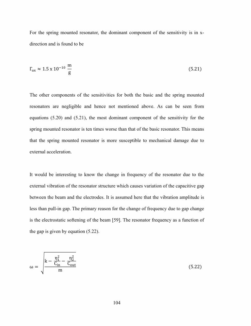
104
For the spring mounted resonator, the dominant component of the sensitivity is in x-
direction and is found to be
Γ 1.5 x 10 mg 5.21
The other components of the sensitivities for both the basic and the spring mounted
resonators are negligible and hence not mentioned above. As can be seen from
equations (5.20) and (5.21), the most dominant component of the sensitivity for the
spring mounted resonator is ten times worse than that of the basic resonator. This means
that the spring mounted resonator is more susceptible to mechanical damage due to
external acceleration.
It would be interesting to know the change in frequency of the resonator due to the
external vibration of the resonator structure which causes variation of the capacitive gap
between the beam and the electrodes. It is assumed here that the vibration amplitude is
less than pull-in gap. The primary reason for the change of frequency due to gap change
is the electrostatic softening of the beam [59]. The resonator frequency as a function of
the gap is given by equation (5.22).
ω k η
C ηC
m 5.22
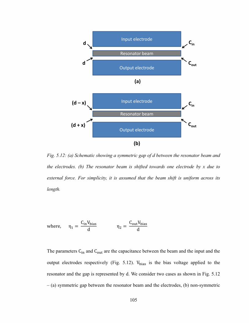
105
Fig. 5.12: (a) Schematic showing a symmetric gap of d between the resonator beam and
the electrodes. (b) The resonator beam is shifted towards one electrode by x due to
external force. For simplicity, it is assumed that the beam shift is uniform across its
length.
where, η C V
d η C V
d
The parameters C and C are the capacitance between the beam and the input and the
output electrodes respectively (Fig. 5.12). V is the bias voltage applied to the
resonator and the gap is represented by d. We consider two cases as shown in Fig. 5.12
– (a) symmetric gap between the resonator beam and the electrodes, (b) non-symmetric
Input electrode
Resonator beam
Output electrode
Input electrode
Resonator beam
Output electrode
(a)
(b)
d
d
Cin
Cout
(d – x) Cin
Cout(d + x)
106
gap due to a shift in the resonator beams. We estimated the resonator frequency for both
the cases using equation (5.22) and found that for 1g acceleration, that is 1.5 x 10⁻¹⁰ m
deformation in the spring supported resonator, the change in frequency is approximately
1 x 10-13. This is several orders of magnitude lower than the affect due to axial stress,
which correlates well with the experimental result described in the previous section
where the change in frequency in the y – direction is buried in the noise and hence not
visible. Hence we conclude that the deformation due to external acceleration does not
lead to any significant change in frequency of the resonator. However, large
deformation due to sudden impact may lead to the failure of the device due to pull-in
effect.
5.3 Vibration Isolation
The spring mounted resonator design reduces the effect of the external vibration on the
resonator frequency. However, it increases the compliance of the resonator structure
resulting in larger deformation for the same external force as compared to that of the
basic resonator. The theoretical analysis described in the previous section does not take
into account the amplification of the resonator deformation due to the lateral resonance
of the structure. There are two resonance modes associated with the resonator. One is
the tuning-fork mode which is the vibration of the resonator beam due to input stimulus
resulting into the output signal called resonator “carrier” frequency, which is
approximately 1.3 MHz for spring mounted resonator. The other one is the lateral-mode
which is the vibration of the entire resonant structure including the springs, which is
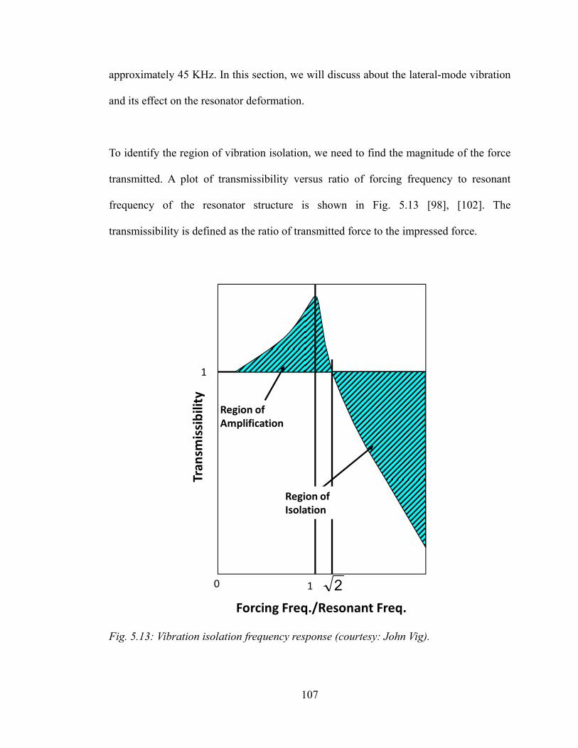
107
approximately 45 KHz. In this section, we will discuss about the lateral-mode vibration
and its effect on the resonator deformation.
To identify the region of vibration isolation, we need to find the magnitude of the force
transmitted. A plot of transmissibility versus ratio of forcing frequency to resonant
frequency of the resonator structure is shown in Fig. 5.13 [98], [102]. The
transmissibility is defined as the ratio of transmitted force to the impressed force.
Fig. 5.13: Vibration isolation frequency response (courtesy: John Vig).
Region ofAmplification
1
0 1 2Forcing Freq./Resonant Freq.
Tran
smissibility
Region ofIsolation
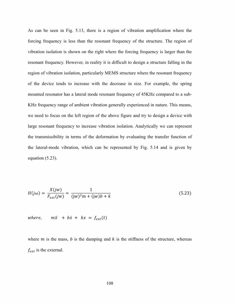
108
As can be seen in Fig. 5.13, there is a region of vibration amplification where the
forcing frequency is less than the resonant frequency of the structure. The region of
vibration isolation is shown on the right where the forcing frequency is larger than the
resonant frequency. However, in reality it is difficult to design a structure falling in the
region of vibration isolation, particularly MEMS structure where the resonant frequency
of the device tends to increase with the decrease in size. For example, the spring
mounted resonator has a lateral mode resonant frequency of 45KHz compared to a sub-
KHz frequency range of ambient vibration generally experienced in nature. This means,
we need to focus on the left region of the above figure and try to design a device with
large resonant frequency to increase vibration isolation. Analytically we can represent
the transmissibility in terms of the deformation by evaluating the transfer function of
the lateral-mode vibration, which can be represented by Fig. 5.14 and is given by
equation (5.23).
1
j m j 5.23
,
where is the mass, is the damping and is the stiffness of the structure, whereas
is the external.
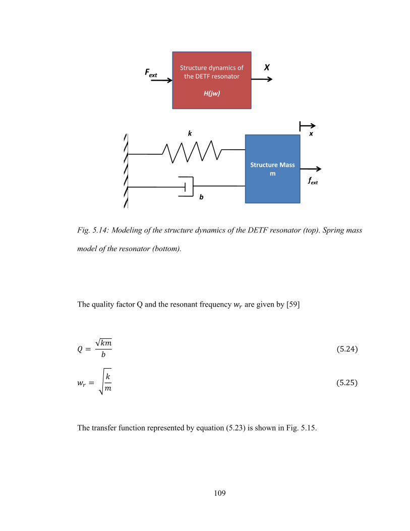
109
Fig. 5.14: Modeling of the structure dynamics of the DETF resonator (top). Spring mass
model of the resonator (bottom).
The quality factor Q and the resonant frequency are given by [59]
√
5.24
5.25
The transfer function represented by equation (5.23) is shown in Fig. 5.15.
Structure Massm
k
b
fext
x
Structure dynamics of the DETF resonator
H(jw)
FextX
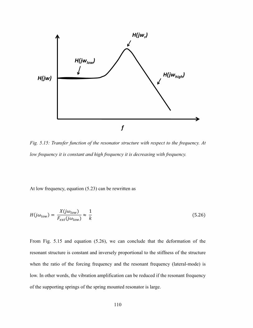
110
Fig. 5.15: Transfer function of the resonator structure with respect to the frequency. At
low frequency it is constant and high frequency it is decreasing with frequency.
At low frequency, equation (5.23) can be rewritten as
1
5.26
From Fig. 5.15 and equation (5.26), we can conclude that the deformation of the
resonant structure is constant and inversely proportional to the stiffness of the structure
when the ratio of the forcing frequency and the resonant frequency (lateral-mode) is
low. In other words, the vibration amplification can be reduced if the resonant frequency
of the supporting springs of the spring mounted resonator is large.
H(jw)
f
H(jwlow)
H(jwr)
H(jwhigh)
111
5.4 Conclusions
Acceleration sensitivity and vibration-induced phase noise are significant problems in
resonator applications. The dominant mechanism of the acceleration sensitivity is axial
stress. A DETF resonator with flexible suspension on both sides exhibits reduced
acceleration and vibration sensitivity, approximately 1000x smaller than the previously
published single anchored DETF micromechanical resonator and 10x smaller than the
SC-cut quartz resonator [87], [97], [98]. One possible disadvantage of this spring
mounted DETF resonator could be the increased flexibility of the structure resulting in a
substantial change in capacitive gap of the electrostatically actuated resonator and
possible damage of the device by snapping the resonator beam into the electrode, under
impact. Also the increased flexibility of this suspension reduces the lateral mode
resonant frequency which is disadvantageous from the vibration isolation point of view.
However, this problem can potentially be mitigated by optimizing the design of the
resonator structure.

112
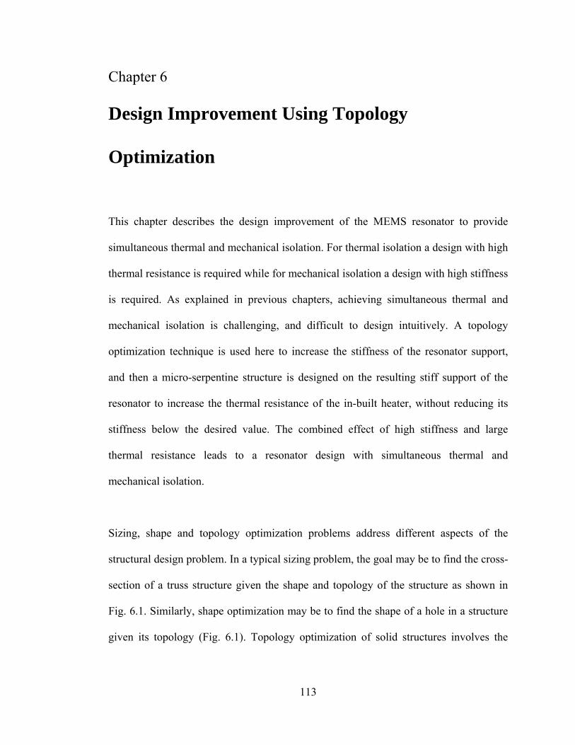
113
Chapter 6
Design Improvement Using Topology
Optimization
This chapter describes the design improvement of the MEMS resonator to provide
simultaneous thermal and mechanical isolation. For thermal isolation a design with high
thermal resistance is required while for mechanical isolation a design with high stiffness
is required. As explained in previous chapters, achieving simultaneous thermal and
mechanical isolation is challenging, and difficult to design intuitively. A topology
optimization technique is used here to increase the stiffness of the resonator support,
and then a micro-serpentine structure is designed on the resulting stiff support of the
resonator to increase the thermal resistance of the in-built heater, without reducing its
stiffness below the desired value. The combined effect of high stiffness and large
thermal resistance leads to a resonator design with simultaneous thermal and
mechanical isolation.
Sizing, shape and topology optimization problems address different aspects of the
structural design problem. In a typical sizing problem, the goal may be to find the cross-
section of a truss structure given the shape and topology of the structure as shown in
Fig. 6.1. Similarly, shape optimization may be to find the shape of a hole in a structure
given its topology (Fig. 6.1). Topology optimization of solid structures involves the
114
determination of features such as the number, location and shape of holes and the
connectivity of the domain; and hence is more fundamental to size and shape.
Fig. 6.1: Structural optimization categorized into size, shape and topology optimization.
(Courtesy: Dr. I. Y. Kim)
6.1 Topology Optimization
In this section, we will discuss the finite element method (FEM) based stiffness
optimization technique. We will first formulate a general stiffness problem in a
mathematical form and then describe a solution method using an optimality criteria
method. This technique is then used to find the shape of the resonator support for the
heater design.
115
6.1.1 Problem Formulation
The purpose of topology optimization is to find the optimal layout of a structure by
distributing the materials in a given region. We will restrict our discussion to the
maximum global stiffness formulation, in other words minimum compliance
formulation. First a general mathematical representation of the minimum compliance
problem will be discussed, and then its discrete form will be presented. We will then
represent the discrete form into a “0 – 1” form which is the backbone of the topology
optimization technique described here. Finally this “0 – 1” form will be modified into a
penalty form to convert the integer variable, 0 and 1, into a continuous variable, making
the problem easier to solve.
6.1.1.1 Minimum Compliance Formulation
To design a structure with maximum global stiffness, we need to design for minimum
compliance or minimum strain energy. The optimum design problem can be defined as
the problem of finding the optimal choice of stiffness tensor Eijkl(x) [103] which is a
variable over the chosen domain. Introducing the energy bilinear form (i.e., the internal
virtual work of an elastic body at the equilibrium u and for an arbitrary virtual
displacement v):
, Ω 6.1
116
with linearized strains
12 6.2
and the load linear form in the absence of any traction force is
Ω 6.3
where f is the body force.
The minimum compliance (maximum global stiffness) problem takes the mathematical
form [103] – [105]
min , , 6.4
. . : , ,
Here U denotes the space of kinematically admissible displacement fields, denotes
the set of admissible stiffness tensors for our design problem. When solving problems
of the form (6.4) computationally, we will discretize the problem domain using finite
elements. There are two fields of interest here, namely the displacement u and the
stiffness E.
117
We can write the discrete form of (6.4) as
min 6.5
. . : ,
Here u and f are the displacement and load vectors, respectively. The global stiffness
matrix K depends on the stiffness in element e, numbered as e = 1,….,N.
The stiffness matrix K is given as
6.6
where is the element stiffness matrix.
6.1.1.2 The “0 – 1” Approach
We are interested in the determination of the optimal placement of a given isotropic
material in space, i.e., we need to know which points of space plays an important role in
taking the load and should be material points, and which points are not required and
should remain void (no material). That is, we need to come up with a geometric
representation of a structure with black-white rendering of an image. In discrete form
this means a black-white representation of the geometry, with pixels given by the finite
118
element discretization [103] – [105]. This implies that the set of admissible
stiffness tensors consists of those tensors for which [103] – [105]:
, 1 Ω 0 Ω\Ω
6.7
Ω Ω ’
Here is called the density function and is the design variable for the minimum
compliance problem. The volume inequality in (6.7) puts a limit, V, on the amount of
the material available, so that the minimum compliance design is for a fixed volume.
The tensor is the stiffness tensor for the given isotropic material, in this case
Silicon. Using equation (6.7), we can now write the “0 – 1” form of (6.5) as
min 6.8
. . : ,
, 1 Ω 0 Ω\Ω
Ω ’
where is the density of the element, and is the volume of that particular element.
119
6.1.1.3 Penalized Density Form
The most commonly used approach to solve the above problem is to replace the integer
variables with continuous variables and then introduce some form of penalty that steers
the solution to discrete 0-1 values. The design problem for the fixed domain is
formulated by modifying the stiffness matrix so that it depends continuously on the
density of the material [103], [106] – [108]. This density function is the design variable.
The requirement is that the optimization results in designs consisting almost entirely of
regions of material or no material. That means the intermediate values of the density
function should be penalized in a manner analogous to the continuous optimization
approximations of 0-1 problems. The penalty form of (6.8) can be written as
min 6.9
. . : , , 1
’, 0 1
The density interpolates between the material properties 0 and such that
0 0, 1
120
6.1.2 Optimality Conditions
In this section, we will find the necessary conditions of optimality for the density of
the minimum compliance design problem, using Optimality Criteria (OC) method. The
OC method has been used in the literature [103], [109] – [113] to solve several
structural optimization problems. We will consider a simple continuum structure with
single load problem. To proceed, we first recapitulate the mathematical form described
in (6.4) with density interpolation function as
min , , 6.10
. . : , ,
,
Ω ’, 0 1
Note that a lower bound is introduced on the density in order to prevent any
possible singularity of the equilibrium problem. For the problems considered here, we
set a typical value of 10 .
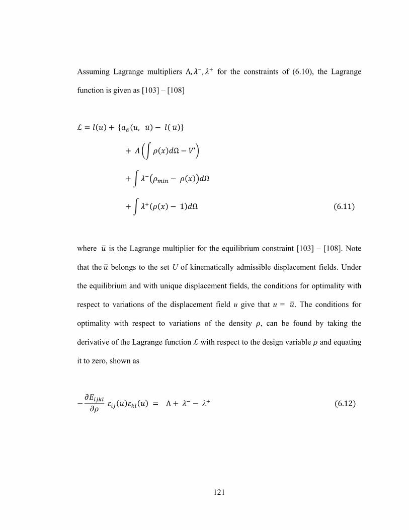
121
Assuming Lagrange multipliers Λ, , for the constraints of (6.10), the Lagrange
function is given as [103] – [108]
,
Ω ’
Ω
1 Ω 6.11
where is the Lagrange multiplier for the equilibrium constraint [103] – [108]. Note
that the belongs to the set U of kinematically admissible displacement fields. Under
the equilibrium and with unique displacement fields, the conditions for optimality with
respect to variations of the displacement field u give that u = . The conditions for
optimality with respect to variations of the density , can be found by taking the
derivative of the Lagrange function with respect to the design variable and equating
it to zero, shown as
Λ 6.12
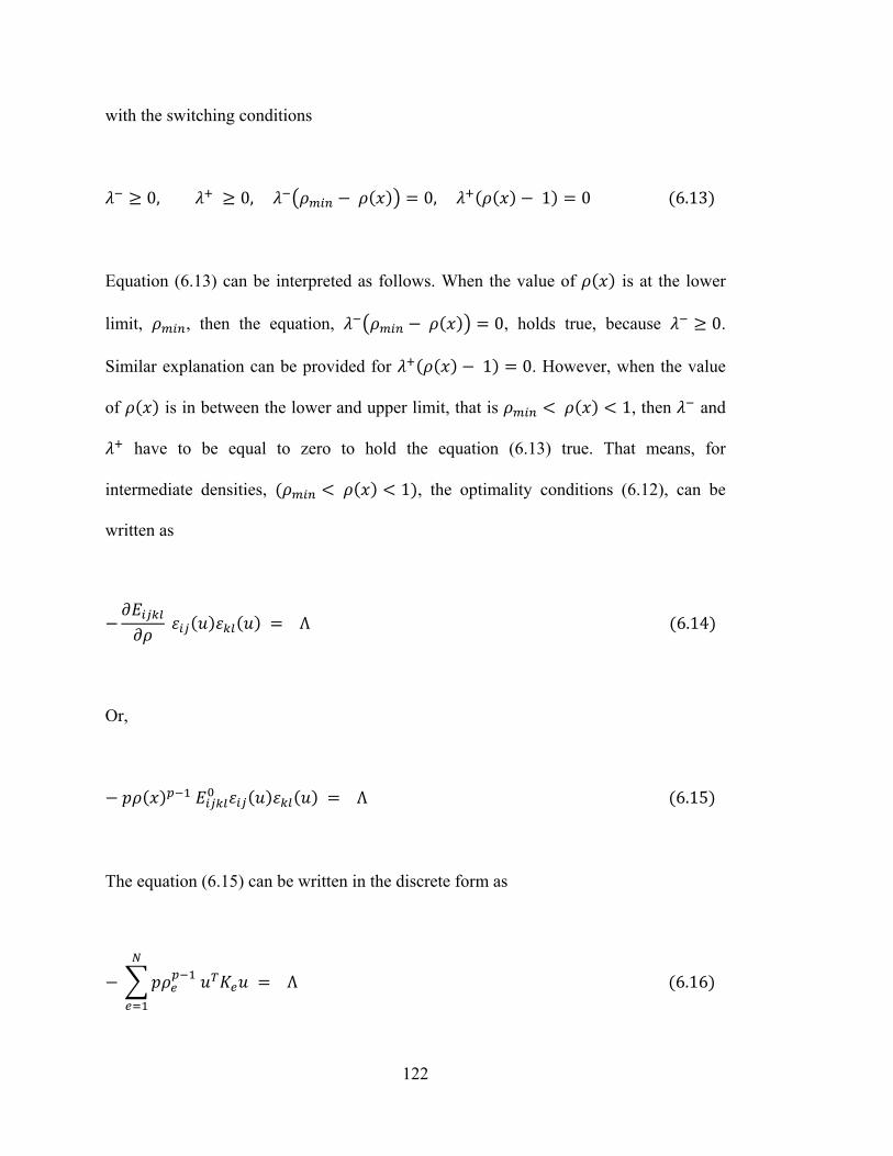
122
with the switching conditions
0, 0, 0, 1 0 6.13
Equation (6.13) can be interpreted as follows. When the value of is at the lower
limit, , then the equation, 0, holds true, because 0.
Similar explanation can be provided for 1 0. However, when the value
of is in between the lower and upper limit, that is 1, then and
have to be equal to zero to hold the equation (6.13) true. That means, for
intermediate densities, 1 , the optimality conditions (6.12), can be
written as
Λ 6.14
Or,
Λ 6.15
The equation (6.15) can be written in the discrete form as
Λ 6.16
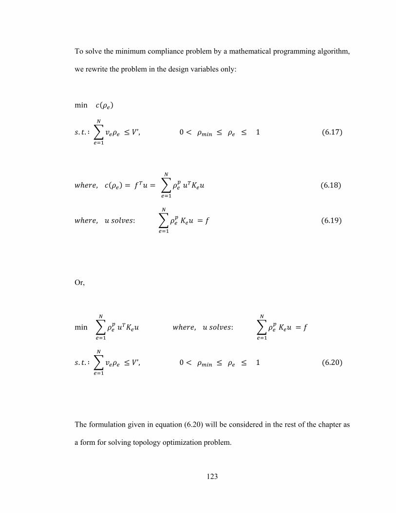
123
To solve the minimum compliance problem by a mathematical programming algorithm,
we rewrite the problem in the design variables only:
min
. . ’, 0 1 6.17
, 6.18
, : 6.19
Or,
min , :
. . ’, 0 1 6.20
The formulation given in equation (6.20) will be considered in the rest of the chapter as
a form for solving topology optimization problem.
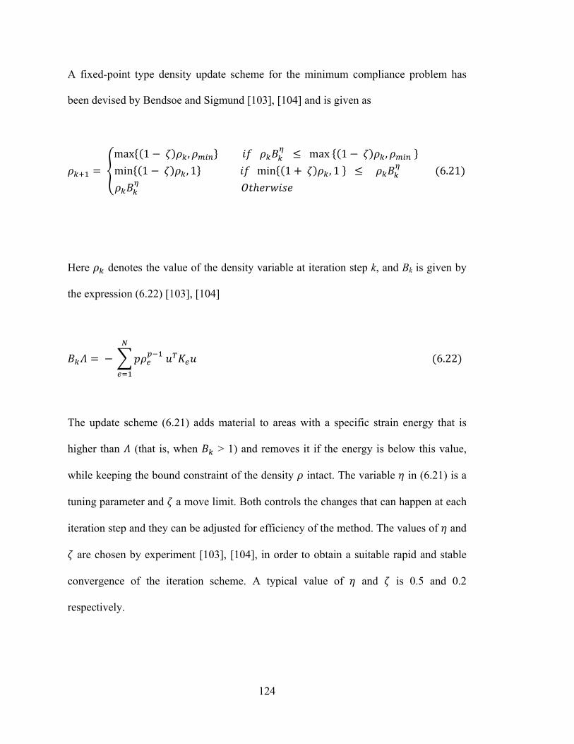
124
A fixed-point type density update scheme for the minimum compliance problem has
been devised by Bendsoe and Sigmund [103], [104] and is given as
max 1 , max 1 , min 1 , 1 min 1 , 1
6.21
Here denotes the value of the density variable at iteration step k, and Bk is given by
the expression (6.22) [103], [104]
6.22
The update scheme (6.21) adds material to areas with a specific strain energy that is
higher than (that is, when > 1) and removes it if the energy is below this value,
while keeping the bound constraint of the density intact. The variable in (6.21) is a
tuning parameter and a move limit. Both controls the changes that can happen at each
iteration step and they can be adjusted for efficiency of the method. The values of and
are chosen by experiment [103], [104], in order to obtain a suitable rapid and stable
convergence of the iteration scheme. A typical value of and is 0.5 and 0.2
respectively.
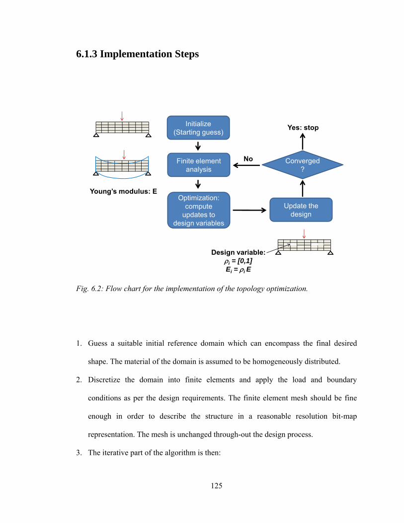
125
6.1.3 Implementation Steps
Fig. 6.2: Flow chart for the implementation of the topology optimization.
1. Guess a suitable initial reference domain which can encompass the final desired
shape. The material of the domain is assumed to be homogeneously distributed.
2. Discretize the domain into finite elements and apply the load and boundary
conditions as per the design requirements. The finite element mesh should be fine
enough in order to describe the structure in a reasonable resolution bit-map
representation. The mesh is unchanged through-out the design process.
3. The iterative part of the algorithm is then:
Initialize(Starting guess)
Finite element analysis
Optimization: compute
updates to design variables
Update the design
Converged?
Yes: stop
No
Design variable:ρi = [0,1]Ei = ρi E
Young’s modulus: E
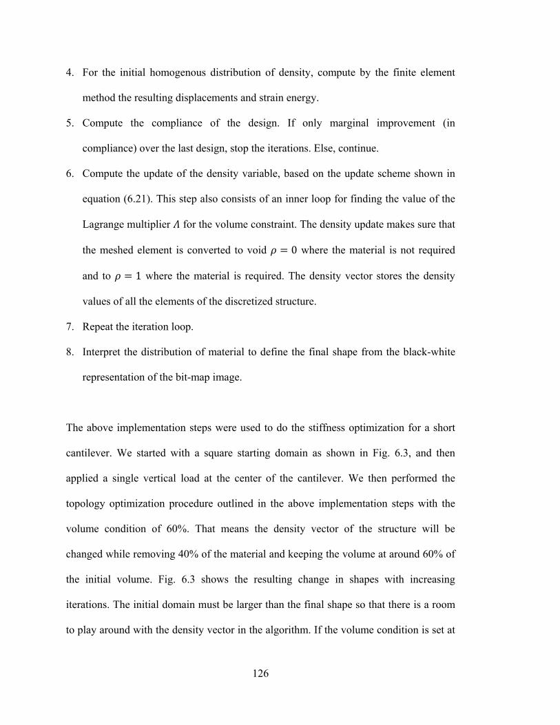
126
4. For the initial homogenous distribution of density, compute by the finite element
method the resulting displacements and strain energy.
5. Compute the compliance of the design. If only marginal improvement (in
compliance) over the last design, stop the iterations. Else, continue.
6. Compute the update of the density variable, based on the update scheme shown in
equation (6.21). This step also consists of an inner loop for finding the value of the
Lagrange multiplier for the volume constraint. The density update makes sure that
the meshed element is converted to void 0 where the material is not required
and to 1 where the material is required. The density vector stores the density
values of all the elements of the discretized structure.
7. Repeat the iteration loop.
8. Interpret the distribution of material to define the final shape from the black-white
representation of the bit-map image.
The above implementation steps were used to do the stiffness optimization for a short
cantilever. We started with a square starting domain as shown in Fig. 6.3, and then
applied a single vertical load at the center of the cantilever. We then performed the
topology optimization procedure outlined in the above implementation steps with the
volume condition of 60%. That means the density vector of the structure will be
changed while removing 40% of the material and keeping the volume at around 60% of
the initial volume. Fig. 6.3 shows the resulting change in shapes with increasing
iterations. The initial domain must be larger than the final shape so that there is a room
to play around with the density vector in the algorithm. If the volume condition is set at
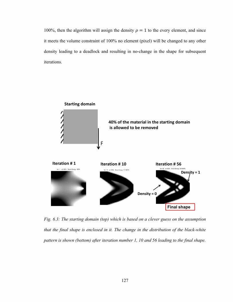
127
100%, then the algorithm will assign the density 1 to the every element, and since
it meets the volume constraint of 100% no element (pixel) will be changed to any other
density leading to a deadlock and resulting in no-change in the shape for subsequent
iterations.
Fig. 6.3: The starting domain (top) which is based on a clever guess on the assumption
that the final shape is enclosed in it. The change in the distribution of the black-white
pattern is shown (bottom) after iteration number 1, 10 and 56 leading to the final shape.
F
Starting domain
40% of the material in the starting domainis allowed to be removed
Iteration # 1 Iteration # 10 Iteration # 56
Density = 0
Density = 1
Final shape
128
It has been shown in the literature [107], [113], [115] – [118] that the above
optimization technique may provide global optimum solution for a simple cantilever
beam under certain circumstances where the error due to discretization and FEM is
small.
It is also very simple to extend the algorithm to account for multiple load cases. In fact,
this can done by just modifying the objective function as the sum of multiple
compliances [103], [104], [114], as shown in equation (6.23).
6.23
where n denotes the total number of loads applied to the structure.
We will now use this technique to design the support of the resonator for better
mechanical isolation.
6.2 Resonator Support Design
We need to design the support of the resonator in such a way that it can overcome the
external impact. The effect of the impact can be modeled as the forces experienced by
the resonator as shown in Fig. 6.4. Reaction forces and local moments are created at the
support anchors on both sides (double anchored) of the resonator to counter balance the
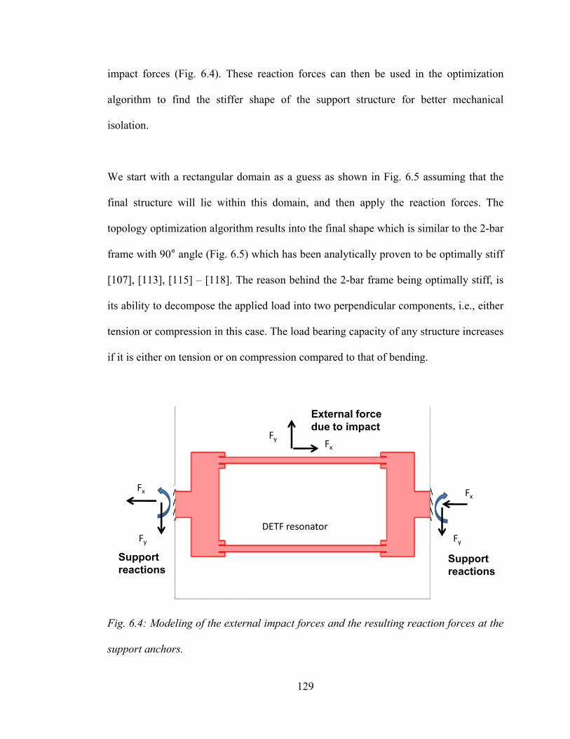
129
impact forces (Fig. 6.4). These reaction forces can then be used in the optimization
algorithm to find the stiffer shape of the support structure for better mechanical
isolation.
We start with a rectangular domain as a guess as shown in Fig. 6.5 assuming that the
final structure will lie within this domain, and then apply the reaction forces. The
topology optimization algorithm results into the final shape which is similar to the 2-bar
frame with 90° angle (Fig. 6.5) which has been analytically proven to be optimally stiff
[107], [113], [115] – [118]. The reason behind the 2-bar frame being optimally stiff, is
its ability to decompose the applied load into two perpendicular components, i.e., either
tension or compression in this case. The load bearing capacity of any structure increases
if it is either on tension or on compression compared to that of bending.
Fig. 6.4: Modeling of the external impact forces and the resulting reaction forces at the
support anchors.
Fx Fx
Fy Fy
Support reactions
DETF resonator
FxFy
External force due to impact
Support reactions
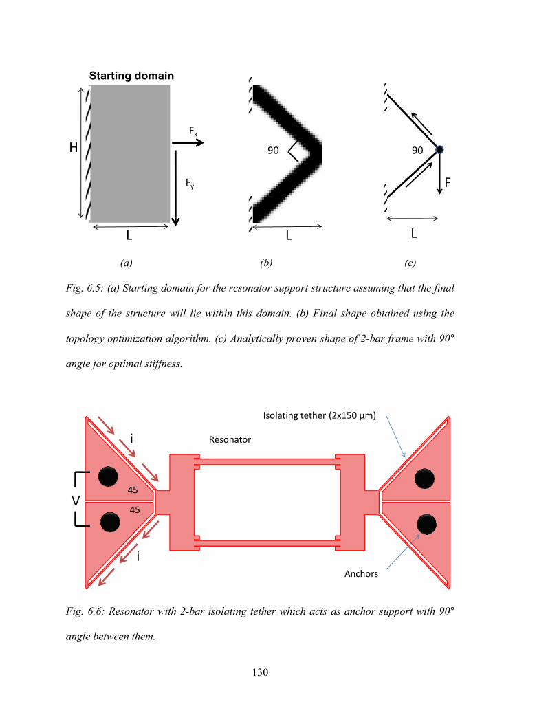
130
(a) (b) (c)
Fig. 6.5: (a) Starting domain for the resonator support structure assuming that the final
shape of the structure will lie within this domain. (b) Final shape obtained using the
topology optimization algorithm. (c) Analytically proven shape of 2-bar frame with 90°
angle for optimal stiffness.
Fig. 6.6: Resonator with 2-bar isolating tether which acts as anchor support with 90°
angle between them.
Starting domain
90
L
HFx
Fy F
90
LL
Isolating tether (2x150 μm)
Anchors
Resonator
45
45
i
i
V
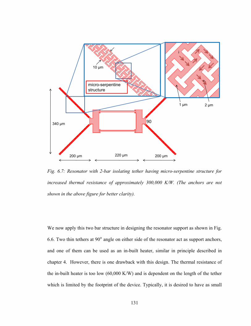
131
Fig. 6.7: Resonator with 2-bar isolating tether having micro-serpentine structure for
increased thermal resistance of approximately 300,000 K/W. (The anchors are not
shown in the above figure for better clarity).
We now apply this two bar structure in designing the resonator support as shown in Fig.
6.6. Two thin tethers at 90° angle on either side of the resonator act as support anchors,
and one of them can be used as an in-built heater, similar in principle described in
chapter 4. However, there is one drawback with this design. The thermal resistance of
the in-built heater is too low (60,000 K/W) and is dependent on the length of the tether
which is limited by the footprint of the device. Typically, it is desired to have as small
Slots creating micro-serpentine structure10 μm
1 μm 2 μm
i
220 μm200 μm 200 μm
340 μm 90
micro-serpentine structure
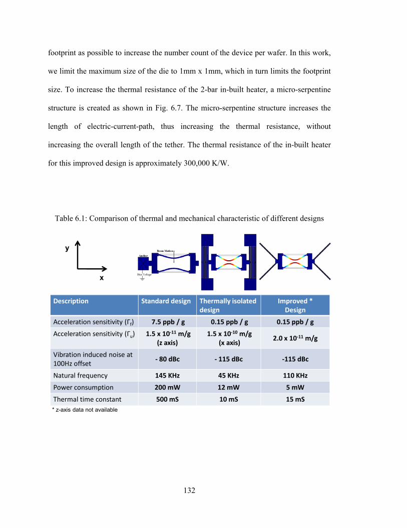
132
footprint as possible to increase the number count of the device per wafer. In this work,
we limit the maximum size of the die to 1mm x 1mm, which in turn limits the footprint
size. To increase the thermal resistance of the 2-bar in-built heater, a micro-serpentine
structure is created as shown in Fig. 6.7. The micro-serpentine structure increases the
length of electric-current-path, thus increasing the thermal resistance, without
increasing the overall length of the tether. The thermal resistance of the in-built heater
for this improved design is approximately 300,000 K/W.
Table 6.1: Comparison of thermal and mechanical characteristic of different designs
Description Standard design Thermally isolated design
Improved * Design
Acceleration sensitivity (Гf) 7.5 ppb / g 0.15 ppb / g 0.15 ppb / g
Acceleration sensitivity (Гu) 1.5 x 10‐11 m/g(z axis)
1.5 x 10‐10 m/g(x axis)
2.0 x 10‐11 m/g
Vibration induced noise at 100Hz offset
‐ 80 dBc ‐ 115 dBc ‐115 dBc
Natural frequency 145 KHz 45 KHz 110 KHz
Power consumption 200 mW 12 mW 5 mW
Thermal time constant 500 mS 10 mS 15 mS
x
y
* z-axis data not available
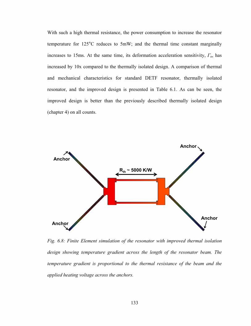
133
With such a high thermal resistance, the power consumption to increase the resonator
temperature for 125°C reduces to 5mW; and the thermal time constant marginally
increases to 15ms. At the same time, its deformation acceleration sensitivity, Гu, has
increased by 10x compared to the thermally isolated design. A comparison of thermal
and mechanical characteristics for standard DETF resonator, thermally isolated
resonator, and the improved design is presented in Table 6.1. As can be seen, the
improved design is better than the previously described thermally isolated design
(chapter 4) on all counts.
Fig. 6.8: Finite Element simulation of the resonator with improved thermal isolation
design showing temperature gradient across the length of the resonator beam. The
temperature gradient is proportional to the thermal resistance of the beam and the
applied heating voltage across the anchors.
Rth ~ 5000 K/W
Anchor
AnchorAnchor
Anchor
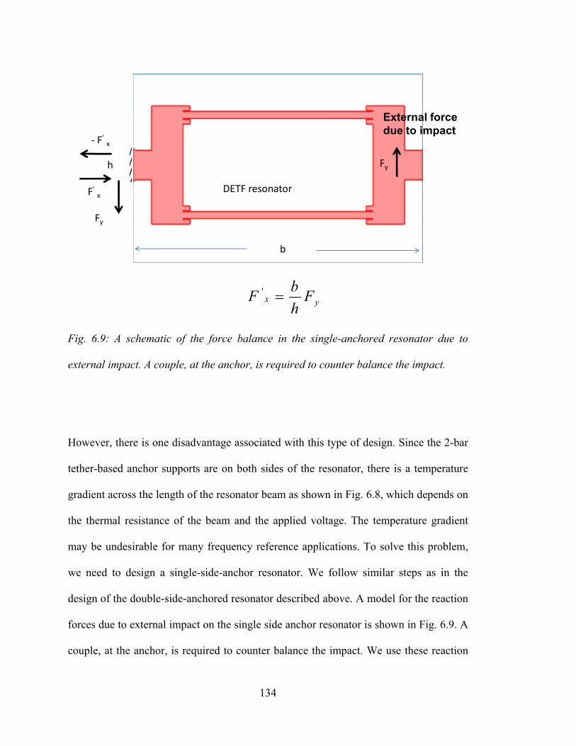
134
Fig. 6.9: A schematic of the force balance in the single-anchored resonator due to
external impact. A couple, at the anchor, is required to counter balance the impact.
However, there is one disadvantage associated with this type of design. Since the 2-bar
tether-based anchor supports are on both sides of the resonator, there is a temperature
gradient across the length of the resonator beam as shown in Fig. 6.8, which depends on
the thermal resistance of the beam and the applied voltage. The temperature gradient
may be undesirable for many frequency reference applications. To solve this problem,
we need to design a single-side-anchor resonator. We follow similar steps as in the
design of the double-side-anchored resonator described above. A model for the reaction
forces due to external impact on the single side anchor resonator is shown in Fig. 6.9. A
couple, at the anchor, is required to counter balance the impact. We use these reaction
‐ F’ x
Fy
DETF resonatorF’ x
h
b
yx FhbF ='
Fy
External force due to impact
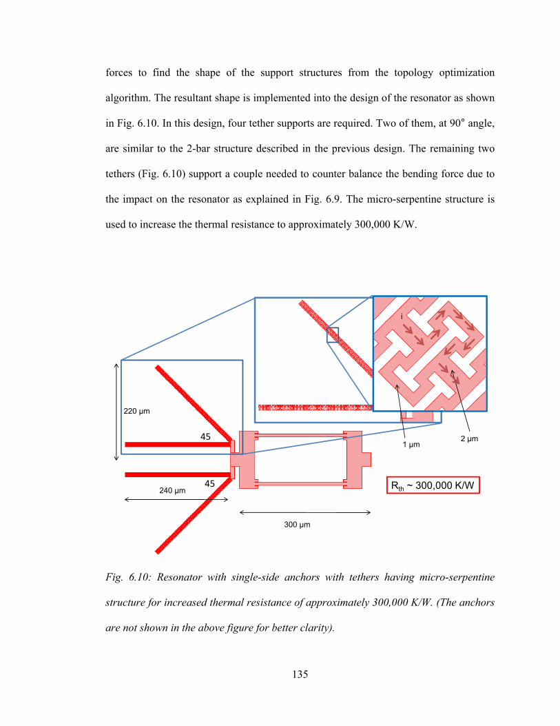
135
forces to find the shape of the support structures from the topology optimization
algorithm. The resultant shape is implemented into the design of the resonator as shown
in Fig. 6.10. In this design, four tether supports are required. Two of them, at 90° angle,
are similar to the 2-bar structure described in the previous design. The remaining two
tethers (Fig. 6.10) support a couple needed to counter balance the bending force due to
the impact on the resonator as explained in Fig. 6.9. The micro-serpentine structure is
used to increase the thermal resistance to approximately 300,000 K/W.
Fig. 6.10: Resonator with single-side anchors with tethers having micro-serpentine
structure for increased thermal resistance of approximately 300,000 K/W. (The anchors
are not shown in the above figure for better clarity).
240 μm
10 μm
300 μm
220 μm
1 μm2 μm
i
45
45 Rth ~ 300,000 K/W
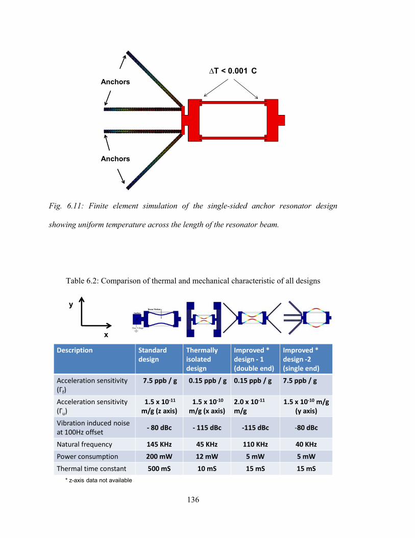
136
Fig. 6.11: Finite element simulation of the single-sided anchor resonator design
showing uniform temperature across the length of the resonator beam.
Table 6.2: Comparison of thermal and mechanical characteristic of all designs
∆T < 0.001 C
Anchors
Anchors
Description Standard design
Thermally isolated design
Improved * design ‐ 1 (double end)
Improved * design ‐2 (single end)
Acceleration sensitivity (Гf)
7.5 ppb / g 0.15 ppb / g 0.15 ppb / g 7.5 ppb / g
Acceleration sensitivity (Гu)
1.5 x 10‐11
m/g (z axis)1.5 x 10‐10
m/g (x axis)2.0 x 10‐11
m/g 1.5 x 10‐10 m/g
(y axis)
Vibration induced noise at 100Hz offset
‐ 80 dBc ‐ 115 dBc ‐115 dBc ‐80 dBc
Natural frequency 145 KHz 45 KHz 110 KHz 40 KHz
Power consumption 200 mW 12 mW 5 mW 5 mW
Thermal time constant 500 mS 10 mS 15 mS 15 mS
* z-axis data not available
x
y
137
The purpose of this design is to keep the temperature of the resonator uniform when
applying the heating voltage. A finite element simulation (Fig. 6.11) shows that the
temperature across the resonator beam is uniform and is within 0.001°C.
However, since the design is single-side anchored, it is more flexible and hence its
deformation acceleration sensitivity, Гu, has reduced by approximately 10x as compared
to the double-side-anchor design. The comparison table 6.2 describes the thermal and
mechanical characteristics of all the designs.
It is to be noted here that the topology optimization technique discussed in this chapter
has been applied only to find the shape of the structure for maximum stiffness. Our goal
was to find the shape of the structure which could optimize both stiffness and thermal
resistance simultaneously. However, it is difficult to analytically model both the
stiffness and the thermal resistance simultaneously for the topology optimization
approach described above, and may require a dedicated research. It is for this reason,
the resonator support design was split into two parts namely stiffness design and the
micro-serpentine design for the thermal resistance, to improve the design as thermally
and mechanically isolated.

138
139
Chapter 7
Conclusions and Future Directions
7.1 Conclusions
In this dissertation, we have presented a technique for high resolution digital
temperature sensor [121], and thermal as well as mechanical isolation of the resonator
[56], [99]. Temperature sensing, thermal isolation and mechanical isolation play
important role in the design of the ovenized silicon micro-mechanical resonator. The
digital temperature sensing technique, described in this work, removes the thermal lag
between the temperature sensor and the resonator. This is crucial in achieving high
precision oven control of the resonator. At the same this sensor can be used as a general
purpose CMOS digital temperature sensor. Thermal isolation is required to reduce the
power consumption and improve the dynamic thermal response of the ovenized
resonator. An overall improvement of approximately 40x and 50x in the power
consumption and the thermal time constant, respectively, have been achieved. An
analysis and improvement of the mechanical isolation of the resonator has also been
described. Topology optimization was used for simultaneous improvement of the
mechanical and thermal isolation of the resonator.
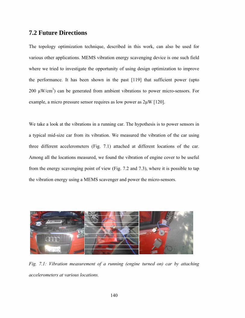
140
7.2 Future Directions
The topology optimization technique, described in this work, can also be used for
various other applications. MEMS vibration energy scavenging device is one such field
where we tried to investigate the opportunity of using design optimization to improve
the performance. It has been shown in the past [119] that sufficient power (upto
200 μW/cm3) can be generated from ambient vibrations to power micro-sensors. For
example, a micro pressure sensor requires as low power as 2μW [120].
We take a look at the vibrations in a running car. The hypothesis is to power sensors in
a typical mid-size car from its vibration. We measured the vibration of the car using
three different accelerometers (Fig. 7.1) attached at different locations of the car.
Among all the locations measured, we found the vibration of engine cover to be useful
from the energy scavenging point of view (Fig. 7.2 and 7.3), where it is possible to tap
the vibration energy using a MEMS scavenger and power the micro-sensors.
Fig. 7.1: Vibration measurement of a running (engine turned on) car by attaching
accelerometers at various locations.
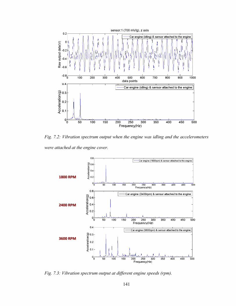
141
Fig. 7.2: Vibration spectrum output when the engine was idling and the accelerometers
were attached at the engine cover.
Fig. 7.3: Vibration spectrum output at different engine speeds (rpm).
1800 RPM
2400 RPM
3600 RPM
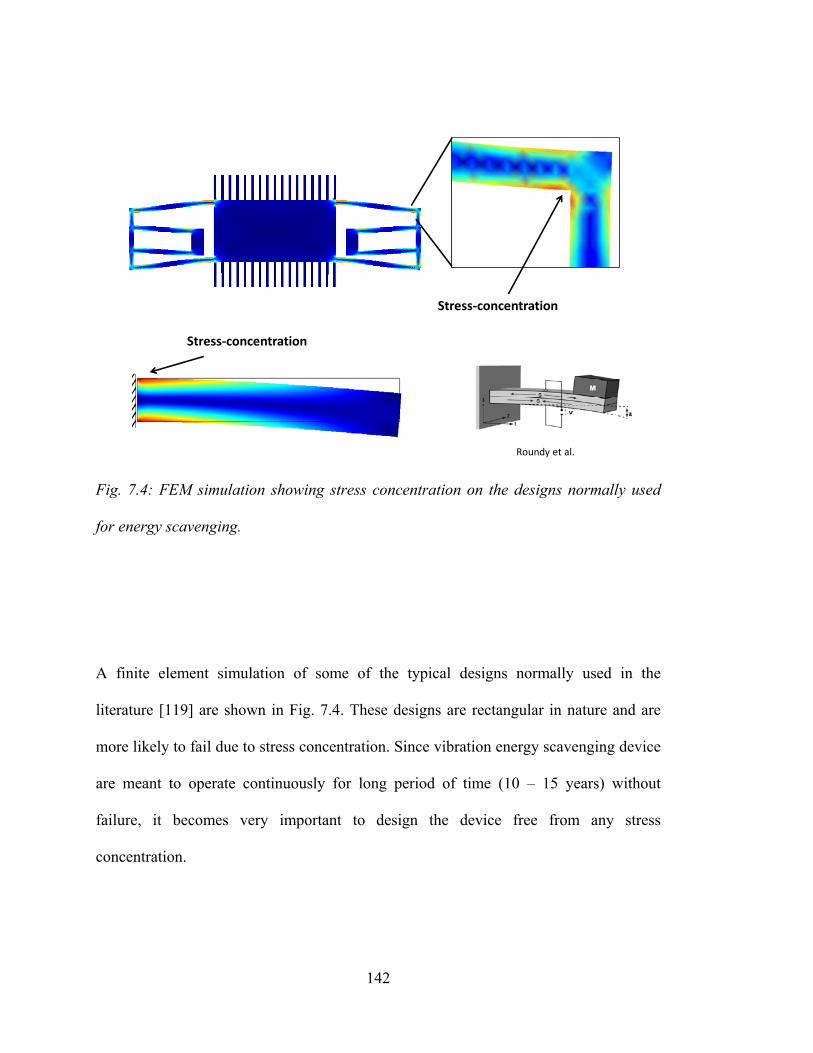
142
Fig. 7.4: FEM simulation showing stress concentration on the designs normally used
for energy scavenging.
A finite element simulation of some of the typical designs normally used in the
literature [119] are shown in Fig. 7.4. These designs are rectangular in nature and are
more likely to fail due to stress concentration. Since vibration energy scavenging device
are meant to operate continuously for long period of time (10 – 15 years) without
failure, it becomes very important to design the device free from any stress
concentration.
Stress‐concentration
Roundy et al.
Stress‐concentration
143
At the same time, the efficiency of the piezoelectric vibration energy scavenger depends
on the stress generated in the beam due to the vibration, and hence there has to be an
optimal stress for a given design of the energy scavenging device. Design (Topology)
optimization can be used to improve the reliability and efficiency of such devices and
hence can be a meaningful future direction.

144
145
References
[1] J. James, and J. Fitz-Randolph, “From Sundials to Atomic Clocks:
Understanding Time and Frequency,” 2nd (revised) edition, Mineola, New
York: Dover Publications, 1999.
[2] A NIST Physics Laboratory http://physics.nist.gov/time
[3] J. James, B. E. Blair, and L. E. Gatterer, “Characterization and Concepts of
Time-Frequency Dissemination,” Proceedings of the IEEE, vol.60, no. 5, May
1972.
[4] W. A. Marrison, and J.W. Horton, "Precision determination of frequency,"
I.R.E. Proc. 16, 137–154, February, 1928.
[5] W. A. Marrison, “The Evolution of the Quartz Crystal Clock," Bell System
Technical Journal 27, 510–588, AT&T, 1948.
[6] M. E. Frerking, Crystal Oscillator Design and Temperature Compensation, New
York, Van Nostrand, 1978.
[7] R. L. Filler, and J. R. Vig, "Resonators for the Microcomputer Compensated
Crystal Oscillator," 43rd Annual Symposium on Frequency Control, 1989.
[8] E. Jackson, and B. Rose, "The Microprocessor Compensated Crystal Oscillator
– New Developments," IEEE, IFCS, 1999.
[9] M. Bloch, M. Meirs, and J. Ho, "The Microcomputer Compensated Crystal
Oscillator (MCXO)," 43rd Annual Symposium on Frequency control, 1989.
[10] A. Benjaminson, and S. C. Stallings, "A Microcomputer-Compensated Crystal
Oscillator using a Dual-Mode Resonator," 43rd Annual Symposium on
Frequency control, 1989.
146
[11] J. R. Vig, “Temperature-insensitive dual-mode resonant sensors—A review,”
IEEE Sensors J., vol. 1, no. 1, pp. 62–68, Jun. 2001.
[12] R. L. Filler, and J. R. Vig, “Resonators for the microcomputer compensated
crystal oscillator,” in Proc. 43rd Annu. Freq. Control Symp., pp. 8–15, 1989.
[13] J. R. Vig, “Temperature stable crystal oscillator,” IEEE Trans. Ultrason.,
Ferroelectr., Freq. Control, vol. 42, no. 4, pp. 797–799, Jul. 1995.
[14] A. Ballato, and J. R. Vig, “Static and dynamic frequency-temperature behavior
of singly and doubly rotated, oven-controlled quartz resonators,” in Proc. 32nd
FCS, pp. 180–188, AD-A955 718, 1978.
[15] I. Balaz, and M. Minarik, “Towards an OCXO with infrared heater,” in Proc.
IEEE Int. FCS, pp. 674–680, 1996.
[16] M. Vaish, “A high precision quartz oscillator with performance comparable to
rubidium oscillators in many respects,” in Proc. IEEE Int. FCS, pp. 752–760,
1996.
[17] Vectron International, C4550 OCXO. http://www.vectron.com
[18] F. G. Major, The Quantum Beat – The Physical Principles of Atomic Clocks,
Springer, Verlag, 1998.
[19] J. Vanier, and C. Audoin, The Quantum Physics of Atomic Frequency
Standards, ISBN, 0-85274-434-X, Adam Hilger, 1978.
[20] L. L. Lewis, “An Introduction to Frequency Standards,” Proc. IEEE, vol. 79, pp.
927-935, 1991.
[21] P. Forman, "Atomichron: The Atomic Clock from Concept to Commercial
Product," Proc. of the IEEE, Vol. 73, No. 7, pp. 1181-1204, July 1985.
147
[22] C. T.-C. Nguyen, “MEMS technology for timing and frequency control,” IEEE
Trans. Ultrason., Ferroelectr., Freq. Control, vol. 54, no. 2, pp. 251–270, Feb.
2007.
[23] V. Kaajakari, J. Kiihamaki, A. Oja, S. Pietikainen, V. Kokkala, and H. Kuisma,
“Stability of wafer level vacuum encapsulated single-crystal silicon resonators,”
Sens. Actuators A, Phys., vol. 130/131, pp. 42–47, Aug. 2006.
[24] C. T.-C. Nguyen, and R. T. Howe, “An integrated CMOS micromechanical
resonator high-Q oscillator,” IEEE J. Solid-State Circuits, vol. 34, no. 4, pp.
440–455, Apr. 1999.
[25] D. Sparks, S. Massoud-Ansari, and N. Najafi, “Chip-level vacuum packaging of
micromachines using nanogetters,” IEEE Trans. Adv. Packag., vol. 26, no. 3,
pp. 277–282, Aug. 2003.
[26] W.-T. Hsu, and C. T.-C. Nguyen, “Stiffness-compensated temperature
insensitive micromechanical resonators,” in Proc. IEEE MEMS, pp. 731–734,
2002.
[27] E. P. Quevy, and R. T. Howe, “Redundant MEMS resonators for precise
reference oscillators,” in Proc. IEEE Radio Freq. Integr. Circuits Symp., pp.
113–116, 2005.
[28] M. A. Hopcroft, M. Agarwal, K. K. Park, B. Kim, C. M. Jha, R. N. Candler, G.
Yama, B. Murmann, and T. W. Kenny, “Temperature compensation of a MEMS
resonator using quality factor as a thermometer,” in Proc. 19th IEEE Int. Conf.
MEMS, pp. 222–225, Jan. 2006.
148
[29] C. T.-C. Nguyen, "Frequency-selective MEMS for miniaturized low-power
communication devices," IEEE Transactions on Microwave Theory and
Techniques, vol. 47, pp. 1486-1503, 1999.
[30] J. W. Weigold, A.-C. Wong, C. T.-C. Nguyen, and S. W. Pang, "A merged
process for thick single-crystal Si resonators and BiCMOS circuitry," IEEE
Journal of Microelectromechanical Systems, vol. 8, pp. 221-228, 1999.
[31] R. A. Buser, and N. F. de Rooij, "Resonant silicon structures," Sensors and
Actuators, vol. 17, pp. 145-154, 1989.
[32] G. Stemme, "Resonant silicon sensors," Journal of Micromechanics and
Microengineering, vol. 1, pp. 113, 1991.
[33] R. N. Kleiman, G. K. Kaminsky, J. D. Reppy, R. Pindak, and D. J. Bishop,
"Single-crystal silicon high-Q torsional oscillators," Review of Scientific
Instruments, vol. 56, pp. 2088-2091, 1985.
[34] R. T. Howe, and R. S. Muller, "Resonant-microbridge vapor sensor," IEEE
Transactions on Electron Devices, vol. 33, pp. 499-506, 1986.
[35] T. P. Burg, A. R. Mirza, N. Milovic, C. H. Tsau, G. A. Popescu, J. S. Foster, and
S. R. Manalis, "Vacuum-Packaged Suspended Microchannel Resonant Mass
Sensor for Biomolecular Detection," Journal Microelectromechanical Systems,
vol. 15, pp. 1466-1476, 2006.
[36] P. Parsons, A. Glendinning, and D. Angelidis, "Resonant sensors for high
accuracy pressure measurement using silicon technology," presented at National
Aerospace and Electronics Conference, NAECON., Proceedings of the IEEE
1992.
149
[37] E. Stemme, and G. Stemme, "A Balanced Resonant Pressure Sensor," Sensors
and Actuators A: Physical, vol. 21, pp. 336-341, 1990.
[38] J. C. Greenwood, "Silicon in mechanical sensors," Journal of Physics E:
Scientific Instruments, pp. 1114-1128, 1988.
[39] T. A. W. Roessig, Integrated MEMS Tuning Fork Oscillators for Sensor
Applications, thesis in Mechanical Engineering at University of California,
Berkeley, 1998.
[40] W. Yun, R. T. Howe, and P. R. Gray, "Surface micromachined, digitally force-
balanced accelerometer with integrated CMOS detection circuitry," presented at
Hilton Head, the IEEE Solid-State Sensor and Actuator Workshop, Hilton Head,
SC USA, 1992.
[41] H. C. Kim, S. Seok, I. Kim, S.-D. Choi, and K. Chun, "Inertial-Grade Out-of-
Plane and In-Plane Differential Resonant Silicon Accelerometers (DRXLs),"
presented at TRANSDUCERS '05, Solid-State Sensors, Actuators and
Microsystems, Seoul, 2005.
[42] W.-T. Hsu, J. R. Clark, and C. T.-C. Nguyen, "A resonant temperature sensor
based on electrical spring softening," presented at TRANSDUCERS ‘01 /
Eurosensors XV, The 11th International Conference on Solid-State Sensors and
Actuators, Munich, Germany, 2001.
[43] L. Lin, R. T. Howe, and A. P. Pisano, "Microelectromechanical filters for signal
processing," Journal of Microelectromechanical Systems, vol. 7, pp. 286-294,
1998.
150
[44] C. T.-C. Nguyen, "Microelectromechanical devices for wireless
communications," MEMS '98, 11th Annual International Workshop on Micro
Electro Mechanical Systems, Heidelberg, Germany, 1998.
[45] Q. Zhong, D. Inniss, K. Kjoller, and V. B. Elings, "Fractured polymer/silica
fiber surface studied by tapping mode atomic force microscopy," Surface
Science, vol. 290, pp. 688-692, 1993.
[46] B. Kim, M. Hopcroft, C. M. Jha, R. Melamud, S. A. Chandorkar, M. Agarwal,
K. L. Chen, W. T. Park, R. Candler, G. Yama, A. Partridge, M. Lutz, and T. W.
Kenny, "Using MEMS to build the device and the package," presented at
Transducers & Eurosensors Lyon, France, 2007.
[47] B. Kim, M. A. Hopcroft, R. Melamud, C. M. Jha, M. Agarwal, S. A. Chandorkar
and T. W. Kenny, "CMOS Compatible Wafer-Scale Encapsulation with MEMS
resonators" ASME InterPACK, Vancouver, Canada, Jul 2007.
[48] B. Kim, R. N. Candler, M. Hopcroft, M. Agarwal, W.-T Park, and T. W. Kenny,
“Frequency Stability of Encapsulated MEMS Resonator,” Sensors and Actuators
A, 136, 125 – 131, 2007.
[49] B. Kim, R. N. Candler, M. Hopcroft, M. Agarwal, W.-T. Park, T. W. Kenny,
"Frequency Stability of Wafer-Scale Encapsulated MEMS Resonators,"
Transducers '05, vol. 2, pp. 1965-1968, 2005.
[50] B. Kim, R. N. Candler, M. Hopcroft, M. Agarwal, W.-T Park, J. Li, and T. W.
Kenny, “Investigation of MEMS Resonators Characteristics for Long-Term
Operation and Wide Temperature Variation Condition,” ASME International
Mechanical Engineering Congress and RD&D Expo, 2004.
151
[51] M. A. Hopcroft, H. K. Lee, B. Kim, R. Melamud, S. Chandorkar, M. Agarwal,
C. M. Jha, J. Salvia, G. Bahl, H. Mehta, and T. W. Kenny, "A High-Stability
MEMS Frequency Reference", TRANSDUCERS '07 / Eurosensors XXI, the
14th International Conference on Solid-State Sensors, Actuators and
Microsystems Lyon, France, 10-14 June 2007.
[52] M. A. Hopcroft, "Silicon Micromechanical Resonators for Frequency
References", Ph.D. thesis in Mechanical Engineering, Stanford University,
2007.
[53] C. T.-C. Nguyen, and R. Howe, “Microresonator frequency control and
stabilization using an integrated micro oven,” in Proc. Transducers, Yokohama,
Japan, pp. 1040–1043, 1993.
[54] C. T.-C. Nguyen, “Micromechanical resonators for oscillators and filters,” in
Proc. IEEE Ultrason. Symp., vol. 1, pp. 489–499, 1995.
[55] M. A. Huff, S. D. Senturia, and R. T. Howe, “Thermally isolated microstructure
suitable for gas sensing applications,” in Tech. Dig. IEEE Solid-State Sens.,
Actuator Workshop, Hilton Head, SC, pp. 47–50, Jun. 6–9, 1988.
[56] C. M. Jha, M. A. Hopcroft, S. A. Chandorkar, J. C. Salvia, M. Agarwal, R. N.
Candler, R. Melamud, B. Kim, and T. W. Kenny, “Thermal Isolation of
Encapsulated MEMS Resonators”, Journal of Microelectromechanical Systems,
vol. 17, no. 1, Feb 2008.
[57] R. N. Candler, M. A. Hopcroft, B. Kim, W. T. Park, R. Melamud, M. Agarwal,
G. Yama, A. Partridge, M. Lutz, and T. W. Kenny, “Longterm and accelerated
life testing of a novel single-wafer vacuum encapsulation for MEMS
152
resonators,” J. Microelectromech. Syst., vol. 15, no. 6, pp. 1446–1456, Dec.
2006.
[58] R. N. Candler, W.-T. Park, H. Li, G. Yama, A. Partridge, M. Lutz, and T. W.
Kenny, “Single wafer encapsulation of MEMS devices,” IEEE Trans. Adv.
Packag., vol. 26, no. 3, pp. 227–232, Aug. 2003.
[59] M. Agarwal, "Nonlinearities and Phase Noise in Electrostatically Transduced
MEMS Resonator based Oscillators", Ph.D. thesis in Electrical Engineering,
Stanford University, 2007.
[60] C. Bourgeois, E. Steinsland, N. Blanc, and N. F. de Rooij, "Design of resonators
for the determination of the temperature coefficients of elastic constants of
monocrystalline silicon," IEEE, The International Frequency Control
Symposium, 1997.
[61] J.-h. Jeong, S.-h. Chung, S.-H. Lee, and D. Kwon, "Evaluation of elastic
properties and temperature effects in Si thin films using an electrostatic
microresonator," Journal of Microelectromechanical Systems, vol. 12, pp. 524-
530, 2003.
[62] S. Nikanorov, Y. A. Burenkov, and A. Stepanov, "Elastic Properties of Silicon,"
Fizika Tverdogo Tela (Soviet Physics Solid State), vol. 13, pp. 3001-4, 1971.
[63] Y. A. Burenkov, and S. Nikanorov, "Temperature dependence of the elastic
constants of silicon," Fizika Tverdogo Tela (Soviet Physics Solid State), vol. 16,
pp. 1496-8, 1974.
153
[64] R. Melamud, M. Hopcroft, C. M. Jha, B. Kim, S. Chandorkar, R. Candler, and
T. W. Kenny, "Effects of Stress on the Temperature Coefficient of Frequency in
Double Clamped Resonators," Transducers '05, vol. 1, pp. 392-395, 2005.
[65] J. C. Greenwood, "Silicon in mechanical sensors," Journal of Physics E:
Scientific Instruments, pp. 1114-1128, 1988.
[66] K. G. Lyon, G. L. Salinger, C. A. Swenson, and G. K. White, "Linear thermal
expansion measurements on silicon from 6 to 340 K," Journal of Applied
Physics, vol. 48, pp. 865-868, 1977.
[67] Y. Okada, and Y. Tokumaru, "Precise determination of lattice parameter and
thermal expansion coefficient of silicon between 300 and 1500 K," Journal of
Applied Physics, vol. 56, pp. 314-320, 1984.
[68] M. J. Madou, Fundamentals of Microfabrication, 2nd ed. (CRC, New York,
1997), pp. 204–207.
[69] R. Melamud, B. Kim, M.A. Hopcroft, S. Chandorkar, M. Agarwal, C.M. Jha,
and T.W. Kenny, "Composite Flexural-Mode Resonator with Controllable
Turnover Temperature," Proceedings of International Conference on MEMS,
Kobe, Japan, 2007.
[70] R. Melamud, B. Kim, S. Chandorkar, M. A. Hopcroft, M. Agarwal, C. M. Jha,
and T. W. Kenny, “Temperature Compensated High Stability Silicon
Resonators,” Appl. Phys. Lett. 90, 1 (2007).
154
[71] S. S. Schodowski, “Resonator Self-Temperature Sensing Using a Dual-
Harmonic-Mode Crystal Oscillator,” Proceedings of the 43rd Annual
Symposium on Frequency Control (IEEE, New York, 1989).
[72] J. R. Vig, “Temperature Insensitive Dual-Mode Resonant Sensors – A Review,”
IEEE Sens. J. 1, 1, Jun. 2001.
[73] A. Barzilai, T. VanZandt, and T. W. Kenny, “Technique for measurement of the
noise of a sensor in the presence of large background signals,” Rev. Sci.
Instrum. 69, 7, Jul. 1998.
[74] J. S. Bendat and A. G. Piersol, Random Data: Analysis and Measurement
Procedures, 2nd ed. (Wiley, New York, 1986), pp. 117–120 and 534–536.
[75] J. S. Bendat and A. G. Piersol, Engineering Applications of Correlation and
Spectral Analysis (Wiley, New York, 1980), pp. 43–48 and 154–159.
[76] D. A. Howe, D. W. Allan, and J. A. Barnes, “Properties of Signal Sources and
Measurement Methods,” Proceedings of the 35th Annual Symposium on
Frequency Control, pp. 1–47, 1981.
[77] M. E. Frerking, Crystal Oscillator Design and Temperature Compensation, New
York: Van Nostrand, 1978.
[78] F. P. Incropera and D. P. Dewitt, Fundamentals of Heat and Mass Transfer, 5th
ed. New York: Wiley, 2002.
[79] M. N. Ozisik, Heat Conduction, 2nd ed. New York: Wiley, 1993.
[80] J. D. Plummer, M. Deal, and P. B. Griffin, Silicon VLSI Technology:
Fundamentals, Practice, and Modeling. Englewood Cliffs, NJ: Prentice-Hall,
2000.
155
[81] A. D. McConnell, U. Srinivasan, and K. E. Goodson, “Thermal conductivity of
doped polysilicon layers,” J. Microelectromech. Syst., vol. 10, no. 3, pp. 360–
369, Sep. 2001.
[82] M. Asheghi, K. Kurabayashi, R. Kasnavi, and K. E. Goodson, “Thermal
conduction in doped single crystal silicon films,” J. Appl. Phys., vol. 91, no. 8,
pp. 5079–5088, Apr. 2002.
[83] W. G. Vincenti and C. H. Kruger, Jr., Introduction to Physical Gas Dynamics.
New York: Wiley, 1975.
[84] V. Kaajakari, T. Mattila, A. Oja, and H. Seppa, “Nonlinear limits for single-
crystal silicon microresonators,” J. Microelectromech. Syst., vol. 13, no. 5, pp.
715–724, Oct. 2004.
[85] R. D. Blevins, Formulas for Natural Frequency and Mode Shape. Malabar, FL:
Krieger, 2000.
[86] S. A. Chandorkar, H. Mehta, M. Agarwal, M. A. Hopcroft, C. M. Jha, R. N.
Candler, G. Yama, G. Bahl, B. Kim, R. Melamud, K. E. Goodson, and T.W.
Kenny, “Non-isothermal micromechanical resonators,” in Proc. MEMS, Kobe,
Japan, 2007.
[87] R. L. Filler, “The acceleration sensitivity of quartz crystal oscillators: a review,”
IEEE transactions on ultrasonic, ferroelectrics and frequency control, vol. 35,
no.3, may 1988.
[88] A. W. Warner and W. L. Smith, “Quartz crystal units and precision oscillators
for operation in severe mechanical environments,” 14th Annu. Symp. Freq.
Contr., 1960, pp. 200-216.
156
[89] W. L. Smith, “An ultra-precise standard of frequency,” Final Report, Contract
DA 36-039 sc-73078, U.S. Army, 1960.
[90] W. J. Spencer and W. L. Smith, “Precision crystal frequency standards,” 15th
Annu. Symp. Freq. Contr., 1961, pp. 139-155.
[91] W. L. Smith and W. J. Spencer, “Quartz crystal controlled oscillators,” Final
Report, Contract DA 36-039 sc-85373, U.S. Army, 1963.
[92] D. B. Leeson, “Aerospace crystal environmental requirements,” 19th Annu.
Symp. Freq. Contr., 1965, pp. 49-57.
[93] D. B. Leeson and G. F. Johnson, “Short-term stability for a Doppler radar:
Requirements, measurements, and techniques,” in Proc. IEEE, 54, 1966, pp.
244-248.
[94] G. F. Johnson, “Vibration characteristics of crystal oscillators.” 21st Annu.
Symp. Freq. Contr., 1967, pp. 287-293.
[95] J. Moses. “NAVSTAR global positioning system oscillator requirements for the
GPS manpack,” 30th Annu. Symp. Freq. Contr., 1967, pp. 390-400.
[96] J. M. Przyjemski and P. L. Konop, “Limitations on GPS receiver performance
imposed by crystal-oscillator g-sensitivity,” NAECON ’77, 1977.
[97] R. Beeson, J. J. Gagnepain, D. Janiaud, and M. Valdois, “Design of a bulk wave
quartz resonator insensitive to acceleration,” Proceedings Freq. Control
Symposium, 1979, p. 337.
[98] J. R. Vig, C. Audoin, L. S. Cutler, M. M. Driscoll, E. P. EerNisse, R. L. Filler,
R. M. Garvey, W. J. Riley, R. C. Smythe, and R. D. Weglein, “Acceleration,
157
Vibration and Shock Effects – IEEE Standards Project P1193,” Proceeding of
the Frequency Control Symposium, 1992, p. 763.
[99] C. M. Jha, J. Salvia, S. A. Chandorkar, R. Melamud, E. Kuhl and T. W. Kenny,
“Acceleration insensitive encapsulated silicon microresonator,” in press APL,
2008.
[100] M. Agarwal, K. K. Park, S. A. Chandorkar, R. N. Candler, B. Kim, M. A.
Hopcroft, R. Melamud, and T. W. Kenny, “Acceleration sensitivity in beam type
electrostatic microresonator,” APL, 90, 014103 (2007).
[101] S. D. Senturia, Microsystem Design, Kluwer academic publishers, Boston, 2001.
[102] J. P. Den Hartog, Mechanical vibrations, Dover publications, Inc. New York,
1985.
[103] M. P. Bendsoe, and O. Sigmund, Topology optimization – theory, methods and
applications, Springer, New York, 2003.
[104] M. P. Bendsoe, and N. Kikuchi, “Generating optimal topologies in structural
design using a homogenization method,” Computers Methods in Applied
Mechanics and Engineering, 71(2), 197 – 224, 1988.
[105] A. Zochowski, “The design of a two dimensional domain,” J. Struct. Mech. 16,
17 – 34, 1988.
[106] M. P. Bendsoe, “Optimal shape design as a material distribution problem,”
Structural Optimization, 1, 193 – 202, 1989.
[107] G. I. N. Rozvany, M. Zhou, and O. Sigmund, “Topology optimization in
structural design,” in H. Adeli (ed.), Advances in Design Optimization,
Chapman and Hall, London, chapter 10, pp. 340 – 399, 1994.
158
[108] R. J. Yang, and C. -H. Chuang, “Optimal topology design using linear
programming,” Computers and Structures, 52(2), 265 – 276, 1994.
[109] W. Prager, and J. E. Taylor, “Problems of optimal structural design,” J. Applied
Mechs., 35, 102 – 106, 1968.
[110] J. E. Taylor, “Maximum strength elastic structural design,” Proc. ASCE, 95, 653
– 663, 1969.
[111] E. F. Masur, “Optimum stiffness and strength of elastic structures,” Journal of
Engineering Mechanics, 96, 621 – 640, 1970.
[112] G. D. Cheng, and N. Olhoff, “Regularized formulation for optimal design of
axisymmetric plates,” International Journal of Solids and Structures, 18(2), 153
– 169, 1982.
[113] G. I. N. Rozvany, and M. Zhou, “The COC algorithm part I: Cross-section
optimization or sizing,” Computer Methods in Applied Mechanics and
Engineering, 89, 281 – 308, 1991.
[114] A. R. Diaz, and M. P. Bendsoe, “Shape optimization of structures for multiple
loading situations using a homogenization method,” Structural Optimization, 4,
17 – 22, 1992.
[115] Y.M.Xie, and G.P.Steven, Evolutionary structural optimization, Springer, New
York 1997.
[116] G. I. N. Rozvany, Optimal design of flexural systems, Pergamon press, Oxford,
1976.
[117] G. I. N. Rozvany, Structural design via optimality criteria, Kluwer Academic
Publishers Group, Dordrecht, Boston, 1989.
159
[118] G. I. N. Rozvany, M. P. Bendsoe, and U. Krisch, “Layout optimization of
structures,” Applied Mechanics Reviews, 48(2), 41 – 119, 1995.
[119] S. J. Roundy, Energy scavenging for wireless sensor nodes with a focus on
vibration to electricity conversion, Thesis, University of California, Berkeley,
2003.
[120] C. Kolle, W. Scherr, D. Hammerschmidt, G. Pichler, M. Motz, B. Schaffer, B.
Forster, and U. Ausserlechner, “Ultra Low-Power Monolithically Integrated
Capacitive Pressure Sensor for Tire Pressure Monitoring,” IEEE, 2004.
[121] C. M. Jha, G. Bahl, R. Melamud, S. A. Chandorkar, M. A. Hopcroft, B. Kim, M.
Agarwal, J. Salvia, H. Mehta, and T. W. Kenny, “High resolution
microresonator based digital temperature sensor,” APL, 91, 7, 2007.
Recommended