The Nexys 4 Number Cruncher
Bassam Jarbo, Donald Burns, Klajdi Lumani, Michael Elias
Electrical and Computer Engineering
Department
School of Engineering and Computer Science Oakland University, Rochester Hills, MI
Abstract:
The purpose of the project was to build a simple
calculator using 7seg displays and switches on the
Nexys 4 DDR FGPA. The calculator would be able to
add, subtract, multiple, and divide 4-bit unsigned
numbers. The project was a great learning experience
for digital logic and VHDL. An example is interfacing
multiple components and performing computations on
the FPGA. The project is going to utilize most of the
skills learned during the ECE 278 course.
Introduction:
The scope of the project was building a 4-bit calculator
using what we learned in our labs and a FPGA (Nexys
4). The team wanted a project that would involve
many topics covered in ECE 278 and challenge the
team to complete the project. This was a good project
to do because it incorporates many different digital
logic principals like architecturally based with
arithmetic operations. Some of the topics that were
covered in class were Arithmetic Logic Unit (ALU)
design, Finite State Machines (FSMs), counters,
multiplexers and priority encoders. Topics that will
need to be researched outside of class will be how to
utilize a debouncer and how to use a serializer. This
project has many applications such as being used as a
traditional calculator or a part of a larger project that
would need calculations performed.
Methodology:
There will be 2 4-bit unsigned inputs. These inputs will
be entered on the bottom of the board using dip
switches. The method of operation will be chosen by
the user. They will activate 1 of 4 preselected
switches. Each switch will correlate with one specific
function. Once that switch is pressed that signal will
go into a debouncer then a priority encoder. An
encoder is used just in case more than one switch is
enabled at one time. A 4x1 multiplexer is used to sort
out the signals then enter a BCD converter then a 7
segment converted which will be sent to a serializer.
The output of the serializer will show on the 7
segment displays. The leftmost 2 displays will show
what the input of A is, the next 2 show the value of B.
The 4 rightmost display will show the whole number
value of the calculation between A and B. If there is a
remainder, it will be displayed on 4 LEDs in unsigned
binary.
The first steps that were taken was to decide what our
inputs and outputs would be. After that we then
collaborated and designed a top level design that we
thought we could successfully implement. After the
top level was created we labeled all signals along with
their sizes. This is important because in portions of the
program input signals must be uniform in order to
avoid any errors. This helped us out a lot when
making the top level design and port mapping. After
that was completed we built each portion of the code.
When all errors were taken care of we moved on to
the top level then the test bench. We tested out
multiple areas to insure everything was working
properly before finally implementing the entire project
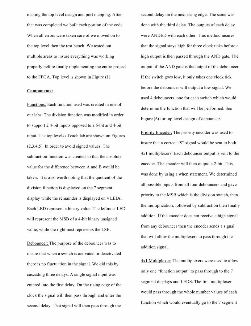
to the FPGA. Top level is shown in Figure (1)
Components:
Functions: Each function used was created in one of
our labs. The division function was modified in order
to support 2 4-bit inputs opposed to a 6-bit and 4-bit
input. The top levels of each lab are shown on Figures
(2,3,4,5). In order to avoid signed values. The
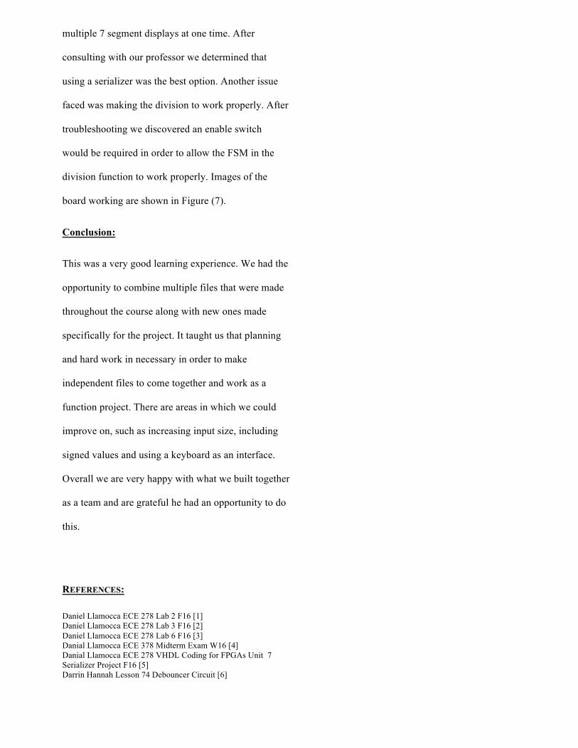
subtraction function was created so that the absolute
value for the difference between A and B would be
taken. It is also worth noting that the quotient of the
division function is displayed on the 7 segment
display while the remainder is displayed on 4 LEDs.
Each LED represent a binary value. The leftmost LED
will represent the MSB of a 4-bit binary unsigned
value, while the rightmost represents the LSB.
Debouncer: The purpose of the debouncer was to
insure that when a switch is activated or deactivated
there is no fluctuation in the signal. We did this by
cascading three delays. A single signal input was
entered into the first delay. On the rising edge of the
clock the signal will then pass through and enter the
second delay. That signal will then pass through the
second delay on the next rising edge. The same was
done with the third delay. The outputs of each delay
were ANDED with each other. This method insures
that the signal stays high for three clock ticks before a
high output is then passed through the AND gate. The
output of the AND gate is the output of the debouncer.
If the switch goes low, it only takes one clock tick
before the debouncer will output a low signal. We
used 4 debouncers, one for each switch which would
determine the function that will be performed. See
Figure (6) for top level design of debouncer.
Priority Encoder: The priority encoder was used to
insure that a correct “S” signal would be sent to both
4x1 multiplexers. Each debouncer output is sent to the
encoder. The encoder will then output a 2-bit. This
was done by using a when statement. We determined
all possible inputs from all four debouncers and gave
priority to the MSB which is the division switch, then
the multiplication, followed by subtraction then finally
addition. If the encoder does not receive a high signal
from any debouncer then the encoder sends a signal
that will allow the multiplexers to pass through the
addition signal.
4x1 Multiplexer: The multiplexers were used to allow
only one “function output” to pass through to the 7
segment displays and LEDS. The first multiplexer
would pass through the whole number values of each
function which would eventually go to the 7 segment
display. The second multiplexer was used to pass
through the remainder from the division function to
the LEDs. If any other function besides division was
chosen, then the second multiplexer would pass
through a value of 0 to the LEDs.
Binary to BCD Converter: We wanted our calculator
to display an output that was in base 10. In order to do
this, we had to convert the outputs of our functions to
binary converted decimal. This was done by making a
table of all possible binary inputs which ranged from
00000000 - 11100001 which is 0 - 225 in decimal. We
limited the output to 225 because the max output of
the calculator would be 15*15. The we made a table
of BCD values with the same range. A when
statement was used to tell allow program to choose the
correct BCD value based on the binary input. Two
different files were created for this, one that could
converter only up to 225 and a second that ranged up
to 4096. This file was made just in case we wanted to
increase out input sizes to 6-bits. Ultimately this file
was not used because the input size was 4-bits and we
didn't want to take up unnecessary memory on the
FPGA.
BCD to 7 segment Converter: This component was
used to send a binary code to the 7 segment display so
that the correct BCD value will be displayed. This was
again done by making a table and using a when
statement.
Serializer: This component was needed to allow
multiple 7 segment displays to appear as if they are all
on at once. A counter was used and set up to interval
every 1 millisecond. The counter output was sent to
the enable of a finite state machine. The FSM had 8
different states, one state for each 7 segment that we
wanted to use. As the counter increases intervals the
FSM goes to the next state. Each state would output a
unique 3-bit value. This unique signal was then sent to
the “S” input of an 8x1 multiplexer and a 3-to-8
decoder. It would then simultaneously allow one input
of the multiplexer to pass through to all 7 segment
displays and enable that inputs corresponding display.
Even though the multiplexers output is sent to each
display, only the one that is enabled will show it. The
inputs of the 8x1 multiplexer are A, B and the output
of the first 4x1 multiplexer. The displays are
flickering once every 8ms for only 1ms. This gives
each display the display frequency of 125hz, which is
too fast for the human eye to notice. Even though the
max output will only need 3 7 segment displays, four
were used. This was done just in case we increased the
input values of A and B.
Results:
We were very well prepared for this project. When
designing and implementing the program we ran into
very few road blocks. One of the roadblocks
encountered was displaying multiple values on
multiple 7 segment displays at one time. After
consulting with our professor we determined that
using a serializer was the best option. Another issue
faced was making the division to work properly. After
troubleshooting we discovered an enable switch
would be required in order to allow the FSM in the
division function to work properly. Images of the
board working are shown in Figure (7).
Conclusion:
This was a very good learning experience. We had the
opportunity to combine multiple files that were made
throughout the course along with new ones made
specifically for the project. It taught us that planning
and hard work in necessary in order to make
independent files to come together and work as a
function project. There are areas in which we could
improve on, such as increasing input size, including
signed values and using a keyboard as an interface.
Overall we are very happy with what we built together
as a team and are grateful he had an opportunity to do
this.
REFERENCES:
Daniel Llamocca ECE 278 Lab 2 F16 [1] Daniel Llamocca ECE 278 Lab 3 F16 [2] Daniel Llamocca ECE 278 Lab 6 F16 [3] Danial Llamocca ECE 378 Midterm Exam W16 [4] Danial Llamocca ECE 278 VHDL Coding for FPGAs Unit 7 Serializer Project F16 [5] Darrin Hannah Lesson 74 Debouncer Circuit [6]
Appendix:
Figure 1- TopLevel
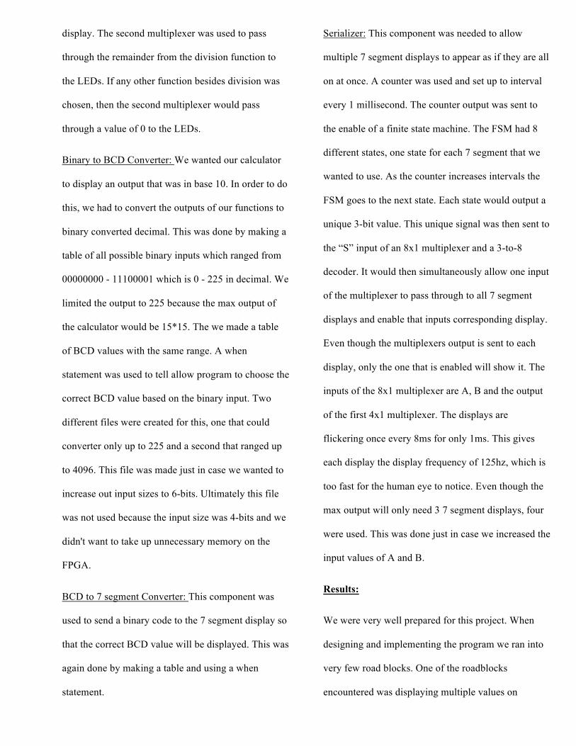
Figure 2 - Addition Toplevel [1]
Figure 3 - Subtraction Toplevel [4]
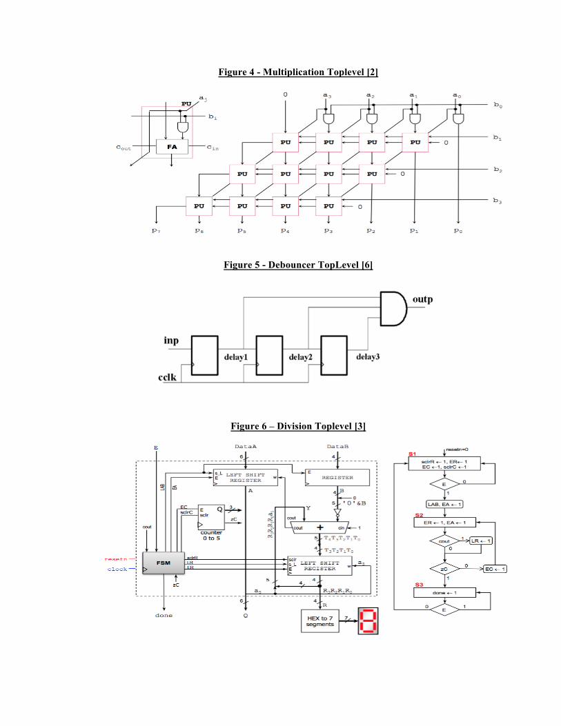
Figure 4 - Multiplication Toplevel [2]
Figure 5 - Debouncer TopLevel [6]
Figure 6 – Division Toplevel [3]
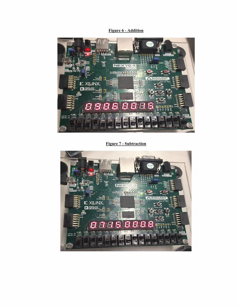
Figure 6 - Addition
Figure 7 - Subtraction
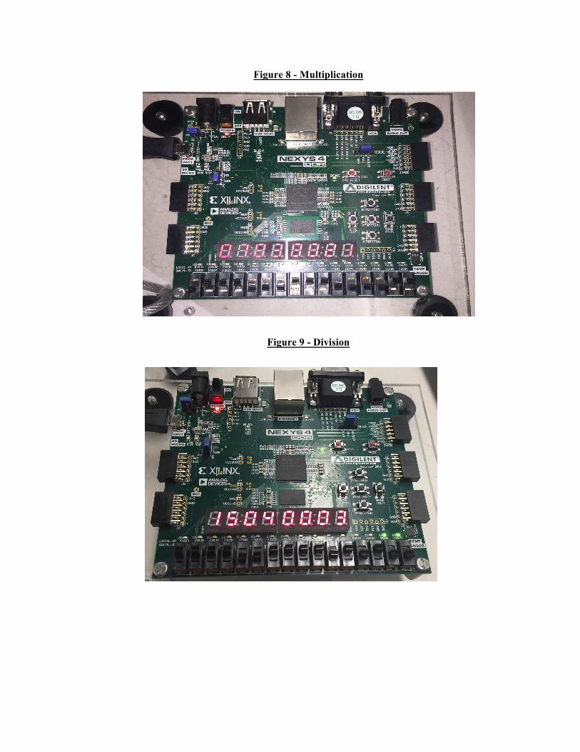
Figure 8 - Multiplication
Figure 9 - Division
Recommended