Dong Lin, Sr. Director, Applications, [email protected] Oliver, VP Corp. Mktg. & IR, [email protected]
The Future of Power: High-Frequency Systems
Enabled by GaNApril 2021
1

World’s first and only GaN power IC companyOver 18Mu shipped and zero failures
3

4

Leonardo da Vinci1452-1519
5

Frustrated Genius:
Strong ideas…
…weak tools
6

The Enabling Force
7

Power GaN Technologies
G
S1S2
D
dMode FET(normally on)
GaN DiscreteComplex gate drive
Extra Si FET in‘cascode’ configuration
Si controller/driver+ Si FET cascode
+ GaN dMode FET
Co-pack
GaN Power ICGaN Power (FET),
Drive, Control, Protection120+ Patents
High Performance Semiconductor
8
• Monolithic integration, 650 V / 800 V, 2 MHz• GaN Power FET(s) + Driver + Control + Protection• Features: on-board regulators, hysteretic input, level-shift,
bootstrap, dV/dt control, UVLO, shoot-through & ESD protection
• “Digital In, Power Out”
Power ICs: Single, Half-Bridge
10…30V
QFN
6 x 8mm
5 x 6mm
2MHz, 0-600V Half-Bridge
SingleGaN Power IC
NV61xx
Half-BridgeGaN Power IC
NV62xx
9

3
2x Energy Savings at 27-40 MHz
• 50% less loss than RF Si• 16x smaller package• Air-core inductors• Minimal FET loss• Negligible gate drive loss
Class Phi-2 DC/AC converter
Technology V Pack(mm)
FSW(MHz)
Eff.(%)
Power(W)
RF Si (ARF521) 500 M17422x22 27.12 91% 150
eMode GaN 650 QFN5x6
27.12 96% 150
40.00 93% 11520ns/div, 150V/div
27.12 MHz, φ2 Inverter, VDS of GaN
10
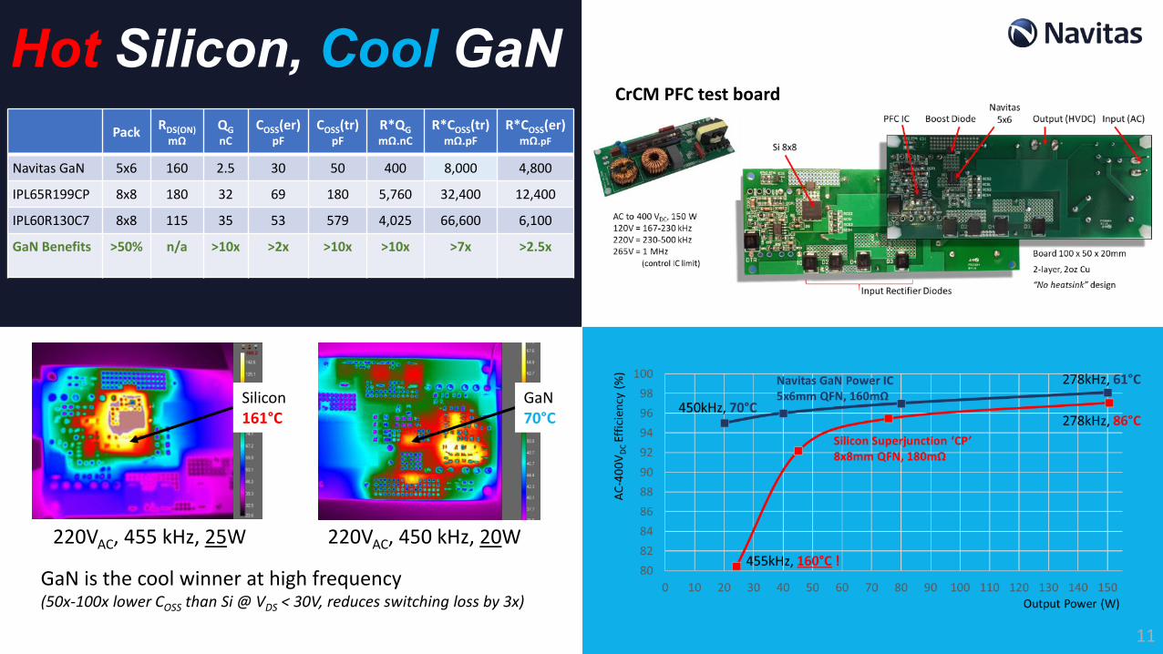
Pack RDS(ON)mΩ
QGnC
COSS(er)pF
COSS(tr)pF
R*QGmΩ.nC
R*COSS(tr)mΩ.pF
R*COSS(er)mΩ.pF
Navitas GaN 5x6 160 2.5 30 50 400 8,000 4,800
IPL65R199CP 8x8 180 32 69 180 5,760 32,400 12,400
IPL60R130C7 8x8 115 35 53 579 4,025 66,600 6,100
GaN Benefits >50% n/a >10x >2x >10x >10x >7x >2.5x
Hot Silicon, Cool GaN
GaN70°C
220VAC, 450 kHz, 20W
Silicon161°C
220VAC, 455 kHz, 25W
GaN is the cool winner at high frequency(50x-100x lower COSS than Si @ VDS < 30V, reduces switching loss by 3x)
CrCM PFC test board
11
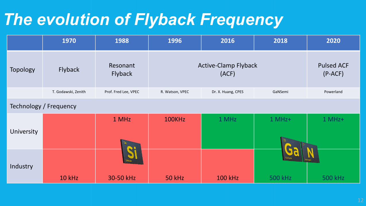
The evolution of Flyback Frequency1970 1988 1996 2016 2018 2020
Topology Flyback Resonant Flyback
Active-Clamp Flyback(ACF)
Pulsed ACF(P-ACF)
T. Godawski, Zenith Prof. Fred Lee, VPEC R. Watson, VPEC Dr. X. Huang, CPES GaNSemi Powerland
Technology / Frequency
University
1 MHz 100KHz 1 MHz 1 MHz+ 1 MHz+
Industry
10 kHz 30-50 kHz 50 kHz 100 kHz 500 kHz 500 kHz
12
3
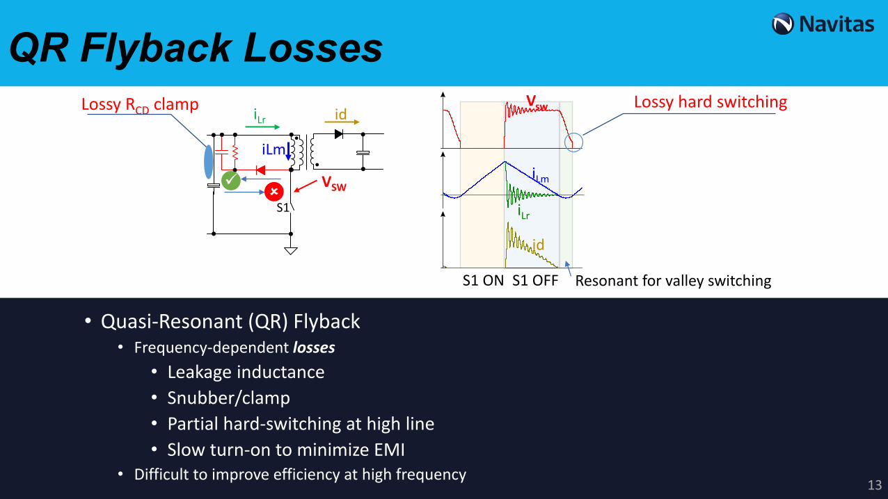
QR Flyback Losses
• Quasi-Resonant (QR) Flyback• Frequency-dependent losses
• Leakage inductance• Snubber/clamp• Partial hard-switching at high line• Slow turn-on to minimize EMI
• Difficult to improve efficiency at high frequency
Resonant for valley switching
iLr
VSW
S1
iLm
id
S1 ON S1 OFF
iLr
Vsw
id
iLm
Lossy RCD clamp Lossy hard switching
13
3
ACF Enables ZVS and High Frequency
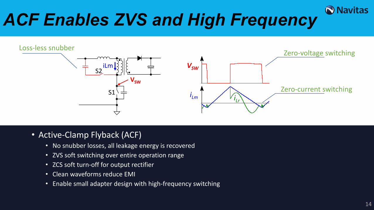
• Active-Clamp Flyback (ACF)• No snubber losses, all leakage energy is recovered• ZVS soft switching over entire operation range• ZCS soft turn-off for output rectifier• Clean waveforms reduce EMI• Enable small adapter design with high-frequency switching
VSW
S1
iLm
Loss-less snubberZero-voltage switching
S2VSW
iLm iLr
Zero-current switching
14

2
Mass Production: ACF
World’s Smallest 65W65W, 53 cc, 1.2 W/cc
2018 2019 2020
World’s Thinnest 45W45W, 41 cc, 1.1 W/cc
‘Pulsed-ACF’World’s Thinnest 50W50W, 34 cc, 1.5 W/cc
15
2
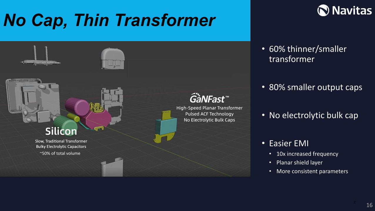
No Cap, Thin Transformer• 60% thinner/smaller
transformer
• 80% smaller output caps
• No electrolytic bulk cap
• Easier EMI• 10x increased frequency• Planar shield layer• More consistent parameters
~50% of total volume
16
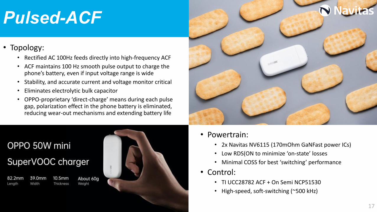
Pulsed-ACF• Topology:
• Rectified AC 100Hz feeds directly into high-frequency ACF• ACF maintains 100 Hz smooth pulse output to charge the
phone’s battery, even if input voltage range is wide• Stability, and accurate current and voltage monitor critical• Eliminates electrolytic bulk capacitor• OPPO-proprietary ‘direct-charge’ means during each pulse
gap, polarization effect in the phone battery is eliminated, reducing wear-out mechanisms and extending battery life
• Powertrain:• 2x Navitas NV6115 (170mOhm GaNFast power ICs)• Low RDS(ON to minimize ‘on-state’ losses• Minimal COSS for best ‘switching’ performance
• Control:• TI UCC28782 ACF + On Semi NCP51530• High-speed, soft-switching (~500 kHz)
17
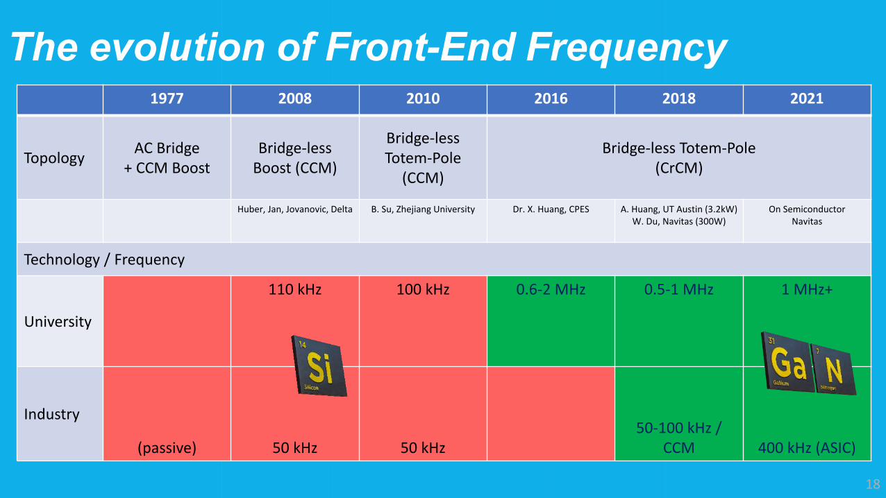
The evolution of Front-End Frequency1977 2008 2010 2016 2018 2021
Topology AC Bridge+ CCM Boost
Bridge-less Boost (CCM)
Bridge-less Totem-Pole
(CCM)
Bridge-less Totem-Pole(CrCM)
Huber, Jan, Jovanovic, Delta B. Su, Zhejiang University Dr. X. Huang, CPES A. Huang, UT Austin (3.2kW)W. Du, Navitas (300W)
On SemiconductorNavitas
Technology / Frequency
University
110 kHz 100 kHz 0.6-2 MHz 0.5-1 MHz 1 MHz+
Industry
(passive) 50 kHz 50 kHz50-100 kHz /
CCM 400 kHz (ASIC)
18
3
Navitas Company Confidential, Under NDA
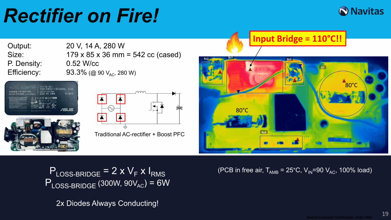
Rectifier on Fire!
PLOSS-BRIDGE = 2 x VF x IRMSPLOSS-BRIDGE (300W, 90VAC) = 6W
2x Diodes Always Conducting!
Input Bridge = 110°C!!
(PCB in free air, TAMB = 25°C, VIN=90 VAC, 100% load)
80°C
Output: 20 V, 14 A, 280 WSize: 179 x 85 x 36 mm = 542 cc (cased)P. Density: 0.52 W/ccEfficiency: 93.3% (@ 90 VAC, 280 W)
Traditional AC-rectifier + Boost PFC
19
80°C
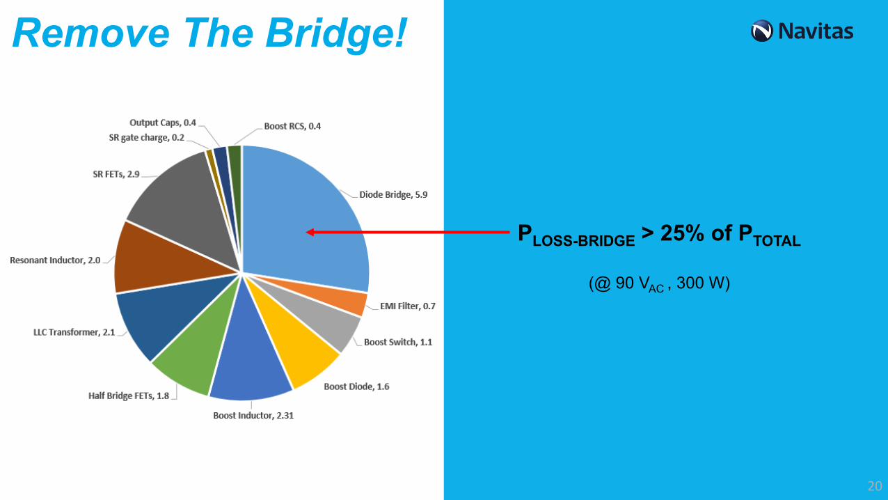
Remove The Bridge!
PLOSS-BRIDGE > 25% of PTOTAL
(@ 90 VAC , 300 W)
20
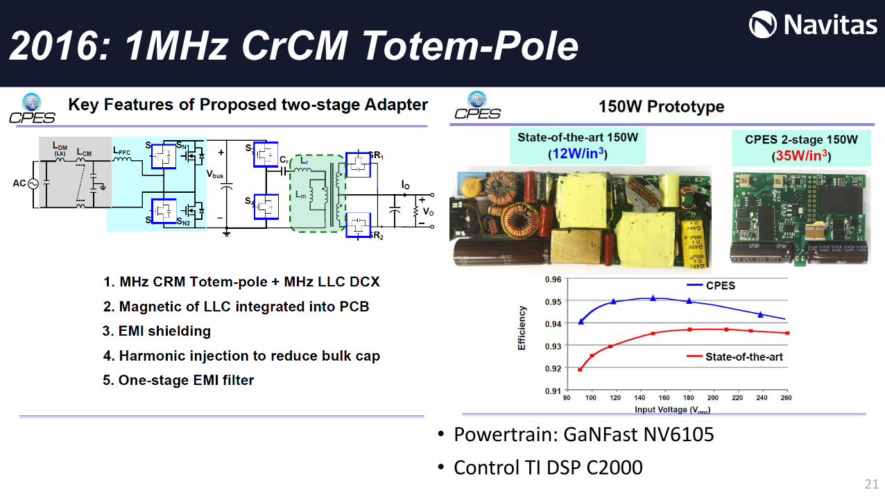
2016: 1MHz CrCM Totem-Pole
• Powertrain: GaNFast NV6105• Control TI DSP C2000
21
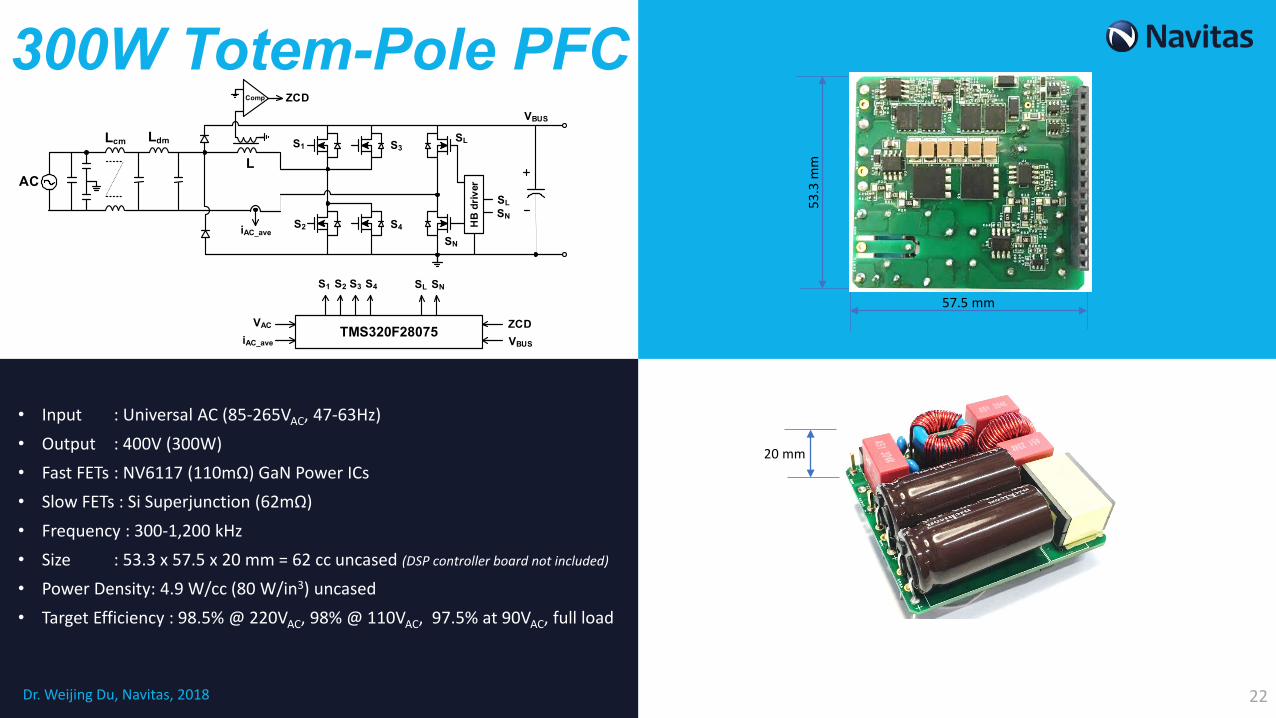
300W Totem-Pole PFC
57.5 mm
53.3
mm
20 mm
SL
VBUS
S2
S1
HB
driv
er
SL
SN
SN
AC
Lcm
L
iAC_ave
TMS320F28075iAC_ave
VAC
S1 S2 SL SN
VBUS
ZCD
S3
S4
ZCDComp
S3 S4
Ldm
• Input : Universal AC (85-265VAC, 47-63Hz)• Output : 400V (300W)• Fast FETs : NV6117 (110mΩ) GaN Power ICs• Slow FETs : Si Superjunction (62mΩ)• Frequency : 300-1,200 kHz• Size : 53.3 x 57.5 x 20 mm = 62 cc uncased (DSP controller board not included)
• Power Density: 4.9 W/cc (80 W/in3) uncased• Target Efficiency : 98.5% @ 220VAC, 98% @ 110VAC, 97.5% at 90VAC, full load
Dr. Weijing Du, Navitas, 2018 22
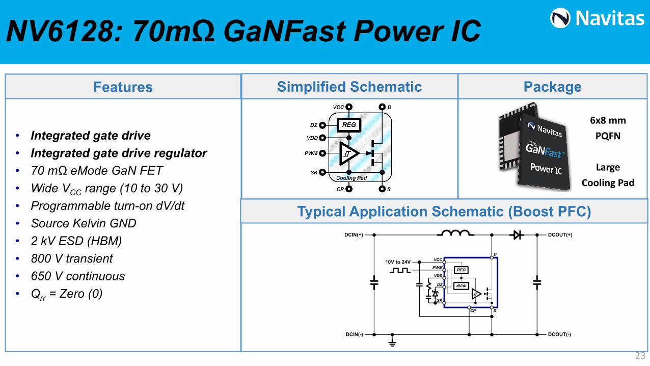
NV6128: 70mΩ GaNFast Power IC
• Integrated gate drive• Integrated gate drive regulator• 70 mΩ eMode GaN FET• Wide VCC range (10 to 30 V)• Programmable turn-on dV/dt• Source Kelvin GND• 2 kV ESD (HBM)• 800 V transient• 650 V continuous• Qrr = Zero (0)
Features Simplified Schematic Package
Typical Application Schematic (Boost PFC)
6x8 mmPQFN
LargeCooling Pad
23

2
High Efficiency, Cool Operation• Bridge + Boost PFC = 96%• CrCM Totem-Pole PFC = 97.5%• Totem-pole = +1.5% !
Fast GaN IC 67°C-71 ° C
Slow Si ~ 55°C
2x NV6128 GaN ICDaughter Card
NCP1680 Totem-Pole PWMPFC InductorEMI Filter
96.0%
96.5%
97.0%
97.5%
98.0%
98.5%
99.0%
99.5%
100.0%
0 50 100 150 200 250 300
Effic
ienc
y (%
)
Output Power (W)
Efficiency vs. Output Power
97.5%Full Load
90 V
110 V
220 V265 V
24

NV6128
Integration Drives Performance
IntegratedGate Driver
IntegratedGaN gate
+ = Zero Gate-SourceLoop Impedance
25
Gate driver loop
𝑳𝑳𝒔𝒔
VDD
VIN
𝑹𝑹𝒅𝒅𝒅𝒅𝒅𝒅𝒅𝒅𝑳𝑳𝒈𝒈
𝑳𝑳𝑳𝒔𝒔
𝑳𝑳𝒅𝒅
𝑳𝑳𝒍𝒍𝒍𝒍𝒅𝒅𝒅𝒅
Driver HV power FET
VOUT
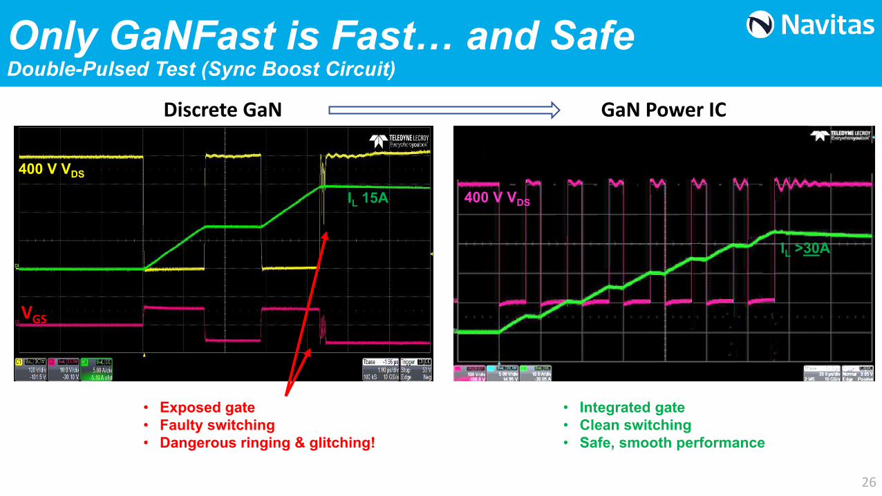
Only GaNFast is Fast… and SafeDouble-Pulsed Test (Sync Boost Circuit)
400 V VDS
IL >30A
VGS
IL 15A
400 V VDS
• Exposed gate• Faulty switching• Dangerous ringing & glitching!
GaN Power ICDiscrete GaN
• Integrated gate• Clean switching• Safe, smooth performance
26
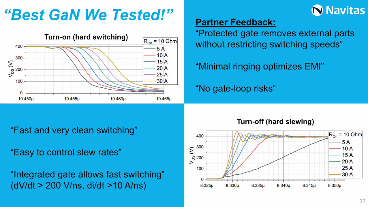
“Best GaN We Tested!”Turn-on (hard switching)
“Fast and very clean switching”
“Easy to control slew rates”
“Integrated gate allows fast switching”(dV/dt > 200 V/ns, di/dt >10 A/ns)
Turn-off (hard slewing)
Partner Feedback:“Protected gate removes external parts without restricting switching speeds”
“Minimal ringing optimizes EMI”
“No gate-loop risks”
27

2
High-Frequency HVDCQuarter (¼) Brick, 400 VIN
GaNFast Power ICs92.5-94.5%
400 kHz
2015 Si150 W
2020 GaN300 W
2x Power
2021 GaN1,000 W6x Power
Best-in-class Si90-92%
GaNFast Power ICs97.0-97.7%
850 kHz28
Recommended