7/30/2019 Tea1733t Lt p Lp
http://slidepdf.com/reader/full/tea1733t-lt-p-lp 1/21
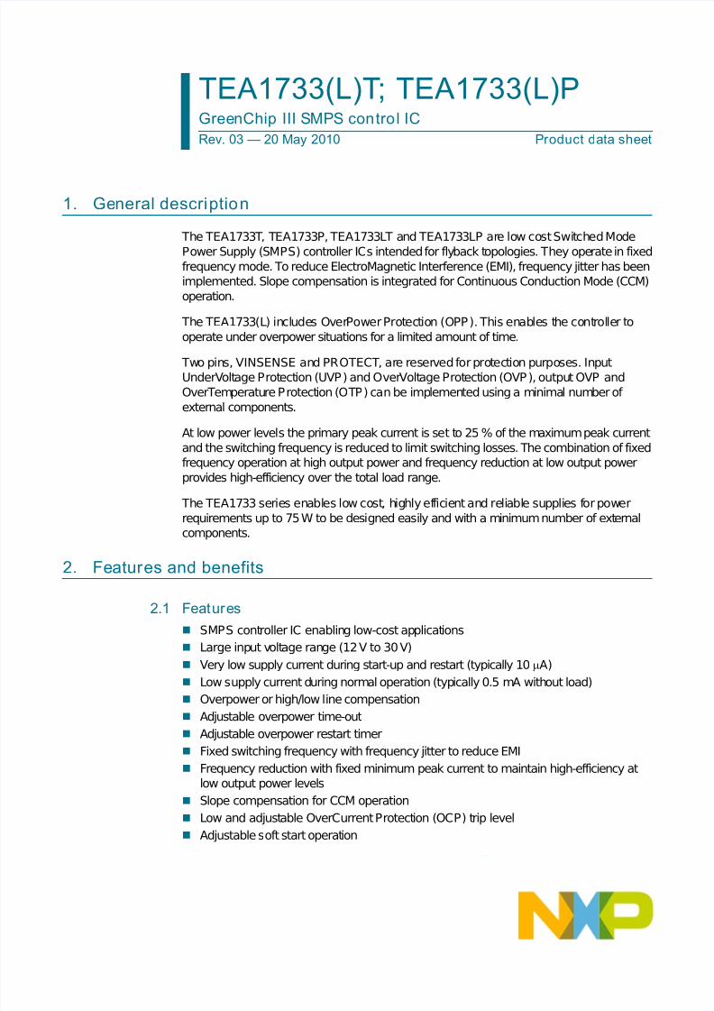
1. General description
The TEA1733T, TEA1733P, TEA1733LT and TEA1733LP are low cost Switched Mode
Power Supply (SMPS) controller ICs intended for flyback topologies. They operate in fixed
frequency mode. To reduce ElectroMagnetic Interference (EMI), frequency jitter has beenimplemented. Slope compensation is integrated for Continuous Conduction Mode (CCM)
operation.
The TEA1733(L) includes OverPower Protection (OPP). This enables the controller to
operate under overpower situations for a limited amount of time.
Two pins, VINSENSE and PROTECT, are reserved for protection purposes. InputUnderVoltage Protection (UVP) and OverVoltage Protection (OVP), output OVP and
OverTemperature Protection (OTP) can be implemented using a minimal number of
external components.
At low power levels the primary peak current is set to 25 % of the maximum peak current
and the switching frequency is reduced to limit switching losses. The combination of fixedfrequency operation at high output power and frequency reduction at low output power
provides high-efficiency over the total load range.
The TEA1733 series enables low cost, highly efficient and reliable supplies for power
requirements up to 75W to be designed easily and with a minimum number of external
components.
2. Features and benefits
2.1 Features
SMPS controller IC enabling low-cost applications
Large input voltage range (12V to 30V)
Very low supply current during start-up and restart (typically 10 μA)
Low supply current during normal operation (typically 0.5 mA without load)
Overpower or high/low line compensation
Adjustable overpower time-out
Adjustable overpower restart timer
Fixed switching frequency with frequency jitter to reduce EMI
Frequency reduction with fixed minimum peak current to maintain high-efficiency atlow output power levels
Slope compensation for CCM operation
Low and adjustable OverCurrent Protection (OCP) trip level
Adjustable soft start operation
TEA1733(L)T; TEA1733(L)PGreenChip III SMPS control IC
Rev. 03 — 20 May 2010 Product data sheet
7/30/2019 Tea1733t Lt p Lp
http://slidepdf.com/reader/full/tea1733t-lt-p-lp 2/21
TEA1733T_LT_P_LP_ 3 All information provided in this document is subject to legal disclaimers. ©NXP B.V. 2010. All rights reserved.
Product data sheet Rev. 03 — 20 May 2010 2 of 21
NXP Semiconductors TEA1733(L)T; TEA1733(L)PGreenChip III SMPS control IC
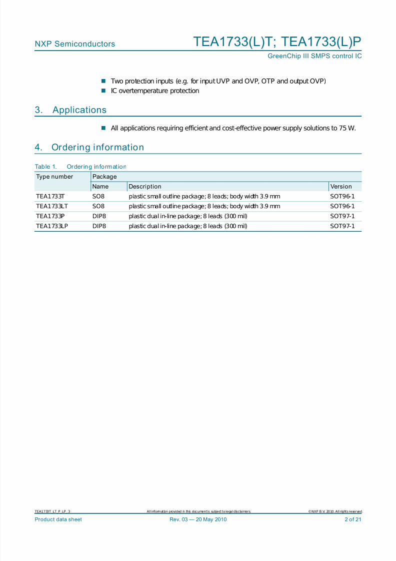
Two protection inputs (e.g. for input UVP and OVP, OTP and output OVP)
IC overtemperature protection
3. Applications
All applications requiring efficient and cost-effective power supply solutions to 75 W.
4. Ordering information
Table 1. Order ing informat ion
Type number Package
Name Description Version
TEA1733T SO8 plastic small outline package; 8 leads; body width 3.9 mm SOT96-1 TEA1733LT SO8 plastic small outline package; 8 leads; body width 3.9 mm SOT96-1
TEA1733P DIP8 plastic dual in-line package; 8 leads (300 mil) SOT97-1
TEA1733LP DIP8 plastic dual in-line package; 8 leads (300 mil) SOT97-1
7/30/2019 Tea1733t Lt p Lp
http://slidepdf.com/reader/full/tea1733t-lt-p-lp 3/21
TEA1733T_LT_P_LP_ 3 All information provided in this document is subject to legal disclaimers. ©NXP B.V. 2010. All rights reserved.
Product data sheet Rev. 03 — 20 May 2010 3 of 21
NXP Semiconductors TEA1733(L)T; TEA1733(L)PGreenChip III SMPS control IC
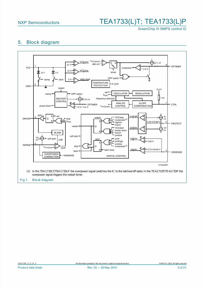
5. Block diagram
(1) In the TEA1733LT/TEA1733LP the overpower signal switches the IC to the latched-off state. In the TEA1733T/TEA1733P theoverpower signal triggers the restart timer.
Fig 1. B lock d iagram
014aaa926
OVERPOWER
CORRECTION
BLANK
OCP
LEB
VINSENSE
latch
stop
soft start
restart
OSCILLATOR
frequency reduction
setδmax
MODULATION
SLOPE
COMPENSATION
ANALOG
CONTROL
restart VCCstopoverpower(1) highvinlowvin
latch
latch reset
DIGITAL CONTROL
soft start55μA
11 μA8
7
2.5 V
1.2 V / 4.5 V
restart
VCCstart D Q
VCCstop
latch reset
RESTART
CONTROL
OPP switch
OTP
OPTIMER
5.4 V
7 kΩ
δmax stop
set
power down
clamp
DRV3
DRIVER
2GND
1VCC
ISENSE4
QS
R
driver
overpowerOPTIMER
CTRL
PROTECT
5
6
VINSENSE
OPP switch
Q
S
R
Q
S
R
clamp latch
21 V
6 V22 V12 V
5 V
400 mV
0.50 V/0.80 V
107μA
32μA
107 μA
prothigh
protlow
highvin
lowvin
3.52 V
0.72 V/0.94 V
VCCstartpower downlowvinprotlow
OTPprothigh
protlowoverpower(1)
Vctrl(Ipeak)
Vctrl(Ipeak)
Vctrl(Ipeak)
TEMPERATURE
PROTECTION
7/30/2019 Tea1733t Lt p Lp
http://slidepdf.com/reader/full/tea1733t-lt-p-lp 4/21
TEA1733T_LT_P_LP_ 3 All information provided in this document is subject to legal disclaimers. ©NXP B.V. 2010. All rights reserved.
Product data sheet Rev. 03 — 20 May 2010 4 of 21
NXP Semiconductors TEA1733(L)T; TEA1733(L)PGreenChip III SMPS control IC
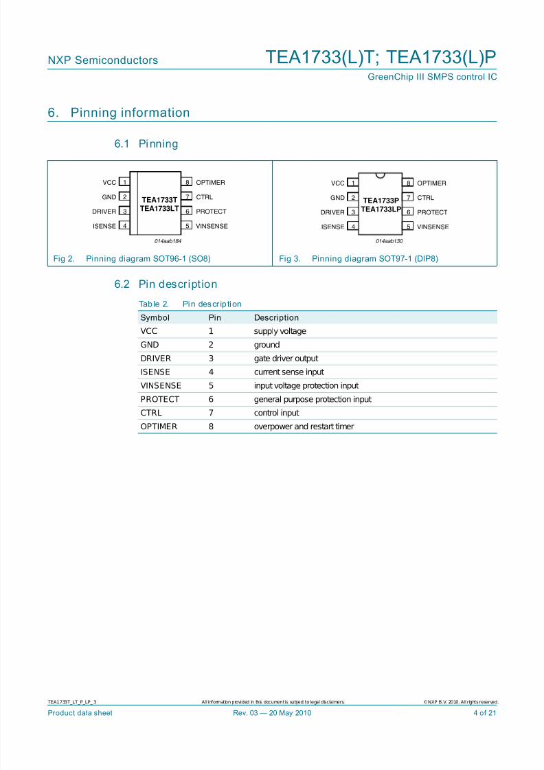
6. Pinning information
6.1 Pinning
6.2 Pin description
Fig 2. Pinning diagram SOT96-1 (SO8) Fig 3. Pinning diagram SOT97-1 (DIP8)
TEA1733TTEA1733LT
VCC OPTIMER
GND CTRL
DRIVER PROTECT
ISENSE VINSENSE
014aab184
1
2
3
4
6
5
8
7TEA1733P
TEA1733LP
VCC OPTIMER
GND CTRL
DRIVER PROTECT
ISENSE VINSENSE
014aab130
1
2
3
4
6
5
8
7
Table 2. Pin descr ip tion
Symbol Pin Description
VCC 1 supply voltage
GND 2 ground
DRIVER 3 gate driver output
ISENSE 4 current sense input
VINSENSE 5 input voltage protection input
PROTECT 6 general purpose protection input
CTRL 7 control input
OPTIMER 8 overpower and restart timer
7/30/2019 Tea1733t Lt p Lp
http://slidepdf.com/reader/full/tea1733t-lt-p-lp 5/21
TEA1733T_LT_P_LP_ 3 All information provided in this document is subject to legal disclaimers. ©NXP B.V. 2010. All rights reserved.
Product data sheet Rev. 03 — 20 May 2010 5 of 21
NXP Semiconductors TEA1733(L)T; TEA1733(L)PGreenChip III SMPS control IC
7. Functional description
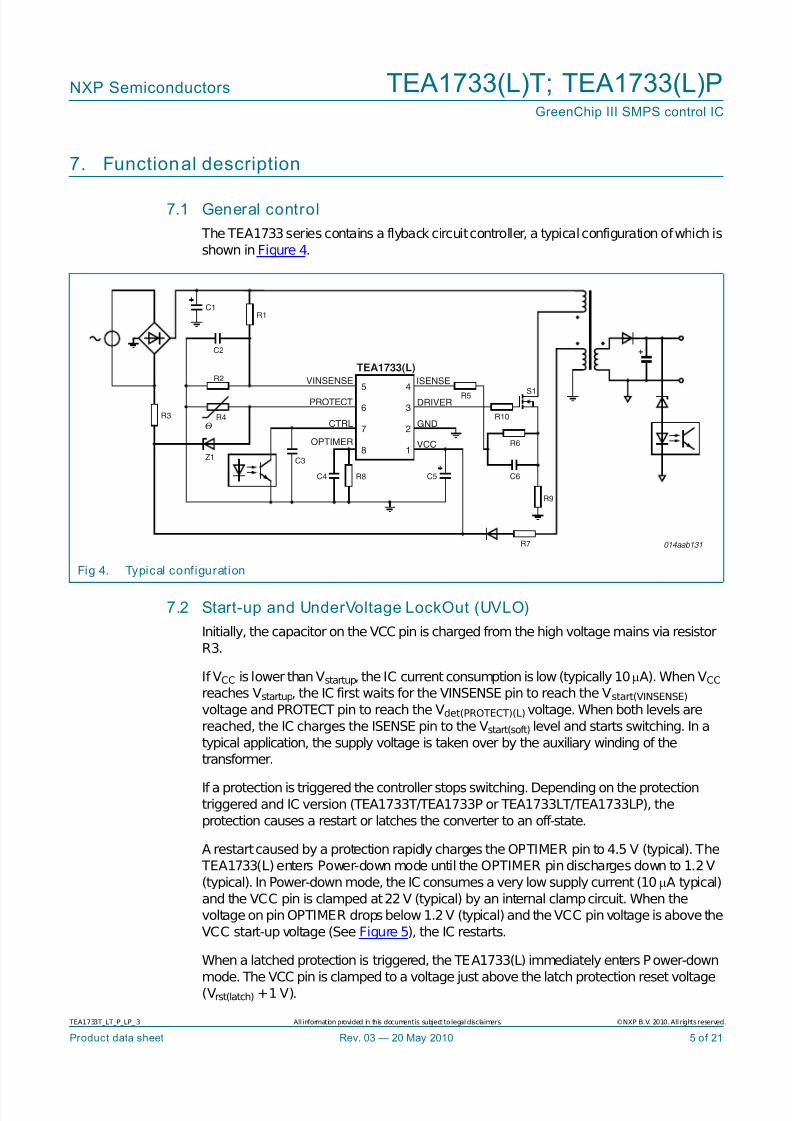
7.1 General control
The TEA1733 series contains a flyback circuit controller, a typical configuration of which is
shown in Figure 4.
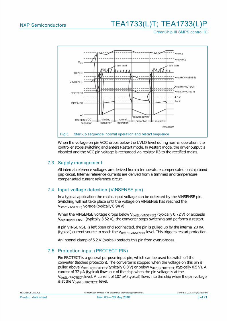
7.2 Start-up and UnderVoltage LockOut (UVLO)
Initially, the capacitor on the VCC pin is charged from the high voltage mains via resistor
R3.
If VCC is lower than Vstartup, the IC current consumption is low (typically 10μA). When VCC reaches Vstartup, the IC first waits for the VINSENSE pin to reach the Vstart(VINSENSE)
voltage and PROTECT pin to reach the Vdet(PROTECT)(L) voltage. When both levels are
reached, the IC charges the ISENSE pin to the Vstart(soft) level and starts switching. In a
typical application, the supply voltage is taken over by the auxiliary winding of thetransformer.
If a protection is triggered the controller stops switching. Depending on the protectiontriggered and IC version (TEA1733T/TEA1733P or TEA1733LT/TEA1733LP), the
protection causes a restart or latches the converter to an off-state.
A restart caused by a protection rapidly charges the OPTIMER pin to 4.5 V (typical). The TEA1733(L) enters Power-down mode until the OPTIMER pin discharges down to 1.2V
(typical). In Power-down mode, the IC consumes a very low supply current (10 μA typical)
and the VCC pin is clamped at 22 V (typical) by an internal clamp circuit. When thevoltage on pin OPTIMER drops below 1.2V (typical) and the VCC pin voltage is above the
VCC start-up voltage (See Figure 5), the IC restarts.
When a latched protection is triggered, the TEA1733(L) immediately enters Power-down
mode. The VCC pin is clamped to a voltage just above the latch protection reset voltage(Vrst(latch) +1 V).
Fig 4. Typical configuration
014aab131
TEA1733(L)
5
6
7
8
4
3
2
1
R1
R2
R3 R4
Z1
C4 R8 C5
R9
C3
C1
C2
R7
C6
R6
R10
S1R5
Θ
DRIVER
GND
VCC
ISENSEVINSENSE
PROTECT
CTRL
OPTIMER
7/30/2019 Tea1733t Lt p Lp
http://slidepdf.com/reader/full/tea1733t-lt-p-lp 6/21
TEA1733T_LT_P_LP_ 3 All information provided in this document is subject to legal disclaimers. ©NXP B.V. 2010. All rights reserved.
Product data sheet Rev. 03 — 20 May 2010 6 of 21
NXP Semiconductors TEA1733(L)T; TEA1733(L)PGreenChip III SMPS control IC
When the voltage on pinVCC drops below the UVLO level during normal operation, thecontroller stops switching and enters Restart mode. In Restart mode, the driver output is
disabled and the VCC pin voltage is recharged via resistor R3 to the rectified mains.
7.3 Supply management
All internal reference voltages are derived from a temperature compensated on-chip bandgap circuit. Internal reference currents are derived from a trimmed and temperature
compensated current reference circuit.
7.4 Input voltage detection (VINSENSE pin)
In a typical application the mains input voltage can be detected by the VINSENSE pin.Switching will not take place until the voltage on VINSENSE has reached the
Vstart(VINSENSE) voltage (typically0.94V).
When the VINSENSE voltage drops below Vdet(L)(VINSENSE) (typically0.72V) or exceedsVdet(H)(VINSENSE) (typically 3.52 V), the converter stops switching and performs a restart.
If pin VINSENSE is left open or disconnected, the pin is pulled up by the internal 20 nA
(typical) current source to reach the Vdet(H)(VINSENSE) level. This triggers restart protection.
An internal clamp of 5.2 V (typical) protects this pin from overvoltages.
7.5 Protection input (PROTECT PIN)
Pin PROTECT is a general purpose input pin, which can be used to switch off the
converter (latched protection). The converter is stopped when the voltage on this pin is
pulled above Vdet(H)(PROTECT) (typically 0.8V) or below Vdet(L)(PROTECT) (typically 0.5 V). Acurrent of 32 μA (typical) flows out of the chip when the pin voltage is at the
Vdet(L)(PROTECT) level. A current of 107 μA (typical) flows into the chip when the pin voltage
is at the Vdet(H)(PROTECT) level.
Fig 5. Start-up sequence, normal operation and restart sequence
014aaa929
starting
convertercharging VCC
capacitor
normal
operationprotection
(power down)
soft start
VCC
ISENSE
VINSENSE
PROTECT
OPTIMER
VO
restart
soft start
Vstartup
Vth(UVLO)
Vdet(H)(VINSENSE)
Vdet(H)(PROTECT)
Vdet(L)(PROTECT)
4.5 V
1.2 V
7/30/2019 Tea1733t Lt p Lp
http://slidepdf.com/reader/full/tea1733t-lt-p-lp 7/21
TEA1733T_LT_P_LP_ 3 All information provided in this document is subject to legal disclaimers. ©NXP B.V. 2010. All rights reserved.
Product data sheet Rev. 03 — 20 May 2010 7 of 21
NXP Semiconductors TEA1733(L)T; TEA1733(L)PGreenChip III SMPS control IC
The PROTECT input can be used to create overvoltage detection and OTP functions.
A small capacitor can be connected to the pin if the protections on this pin are not used.
An internal clamp of 4.1 V (typical) protects this pin from overvoltages.
7.6 Duty cycle control (CTRL pin)
The output power of the converter is regulated by the CTRL pin. This pin is connected to
an internal 5.4 V supply using an internal 7 kΩ resistor.
The CTRL pin voltage sets the peak current which is measured using the ISENSE pin(see Section7.10). At a low output power the switching frequency is also reduced (see
Section 7.12). The maximum duty cycle is limited to 72 %.
7.7 Slope compensation (CTRL pin)
A slope compensation circuit is integrated in the IC or CCM. Slope compensationguarantees stable operation for duty cycles greater than 50 %.
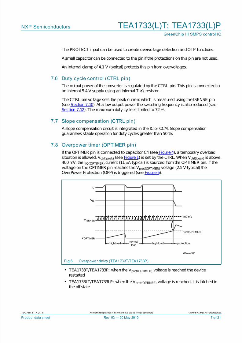
7.8 Overpower timer (OPTIMER pin)
If the OPTIMER pin is connected to capacitor C4 (see Figure4), a temporary overloadsituation is allowed. Vctrl(Ipeak) (see Figure1) is set by the CTRL. When Vctrl(Ipeak) is above
400mV, the IIO(OPTIMER) current (11μA typical) is sourced from the OPTIMER pin. If the
voltage on the OPTIMER pin reaches the Vprot(OPTIMER) voltage (2.5V typical) theOverPower Protection (OPP) is triggered (see Figure6).
• TEA1733T/TEA1733P: when the Vprot(OPTIMER) voltage is reached the devicerestarted
• TEA1733LT/TEA1733LP: when the Vprot(OPTIMER) voltage is reached, it is latched in
the off state
Fig 6. Overpower delay (TEA1733T/TEA1733P)
014aaa930
VOPTIMER
VISENSE
VO
400 mV
protectionhigh loadhigh loadnormal
load
Vprot(OPTIMER)
IO
7/30/2019 Tea1733t Lt p Lp
http://slidepdf.com/reader/full/tea1733t-lt-p-lp 8/21
TEA1733T_LT_P_LP_ 3 All information provided in this document is subject to legal disclaimers. ©NXP B.V. 2010. All rights reserved.
Product data sheet Rev. 03 — 20 May 2010 8 of 21
NXP Semiconductors TEA1733(L)T; TEA1733(L)PGreenChip III SMPS control IC
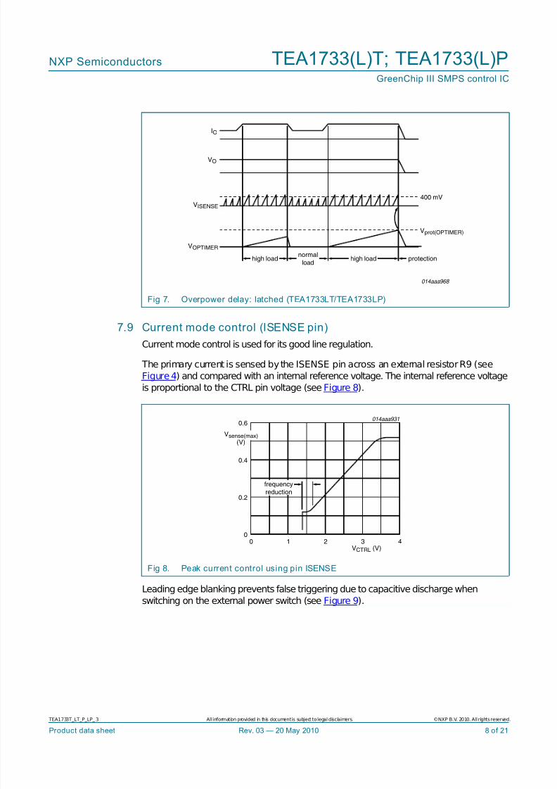
7.9 Current mode control (ISENSE pin)
Current mode control is used for its good line regulation.
The primary current is sensed by the ISENSE pin across an external resistor R9 (see
Figure4) and compared with an internal reference voltage. The internal reference voltage
is proportional to the CTRL pin voltage (see Figure 8).
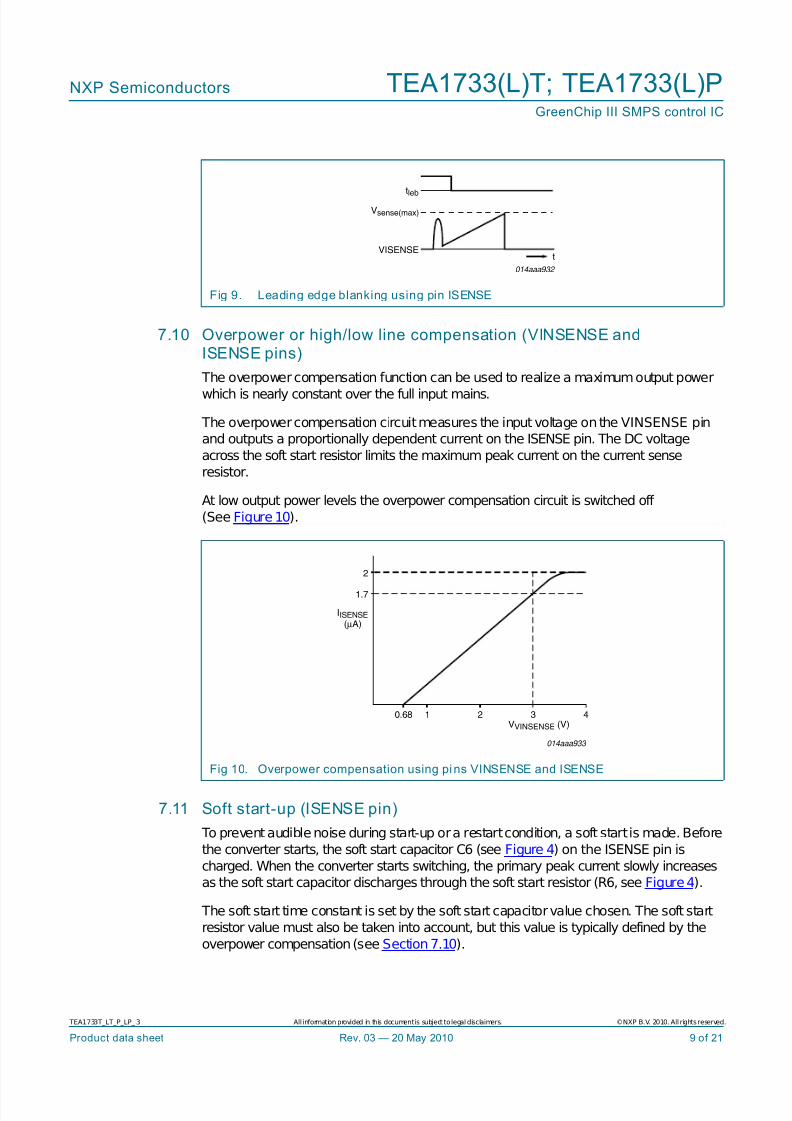
Leading edge blanking prevents false triggering due to capacitive discharge when
switching on the external power switch (see Figure 9).
Fig 7. Overpower delay: latched (TEA1733LT/TEA1733LP)
014aaa968
VOPTIMER
VISENSE
VO
400 mV
protectionhigh loadhigh loadnormal
load
Vprot(OPTIMER)
IO
Fig 8. Peak current control using pin ISENSE
frequency
reduction0.2
0.4
0.6
00 431 2
014aaa931
VCTRL (V)
Vsense(max)(V)
7/30/2019 Tea1733t Lt p Lp
http://slidepdf.com/reader/full/tea1733t-lt-p-lp 9/21
TEA1733T_LT_P_LP_ 3 All information provided in this document is subject to legal disclaimers. ©NXP B.V. 2010. All rights reserved.
Product data sheet Rev. 03 — 20 May 2010 9 of 21
NXP Semiconductors TEA1733(L)T; TEA1733(L)PGreenChip III SMPS control IC
7.10 Overpower or high/low line compensation (VINSENSE andISENSE pins)
The overpower compensation function can be used to realize a maximum output power
which is nearly constant over the full input mains.
The overpower compensation circuit measures the input voltage on the VINSENSE pinand outputs a proportionally dependent current on the ISENSE pin. The DC voltage
across the soft start resistor limits the maximum peak current on the current sense
resistor.
At low output power levels the overpower compensation circuit is switched off
(See Figure10).
7.11 Soft start-up (ISENSE pin)
To prevent audible noise during start-up or a restart condition, a soft start is made. Before
the converter starts, the soft start capacitor C6 (see Figure 4) on the ISENSE pin is
charged. When the converter starts switching, the primary peak current slowly increasesas the soft start capacitor discharges through the soft start resistor (R6, see Figure4).
The soft start time constant is set by the soft start capacitor value chosen. The soft start
resistor value must also be taken into account, but this value is typically defined by the
overpower compensation (see Section7.10).
Fig 9. Leading edge blanking using pin ISENSE
tleb
Vsense(max)
VISENSEt
014aaa932
Fig 10. Overpower compensation using pins VINSENSE and ISENSE
2
1.7
0.68 1 2 3 4
014aaa933
IISENSE(μA)
VVINSENSE (V)
7/30/2019 Tea1733t Lt p Lp
http://slidepdf.com/reader/full/tea1733t-lt-p-lp 10/21
TEA1733T_LT_P_LP_ 3 All information provided in this document is subject to legal disclaimers. ©NXP B.V. 2010. All rights reserved.
Product data sheet Rev. 03 — 20 May 2010 10 of 21
NXP Semiconductors TEA1733(L)T; TEA1733(L)PGreenChip III SMPS control IC
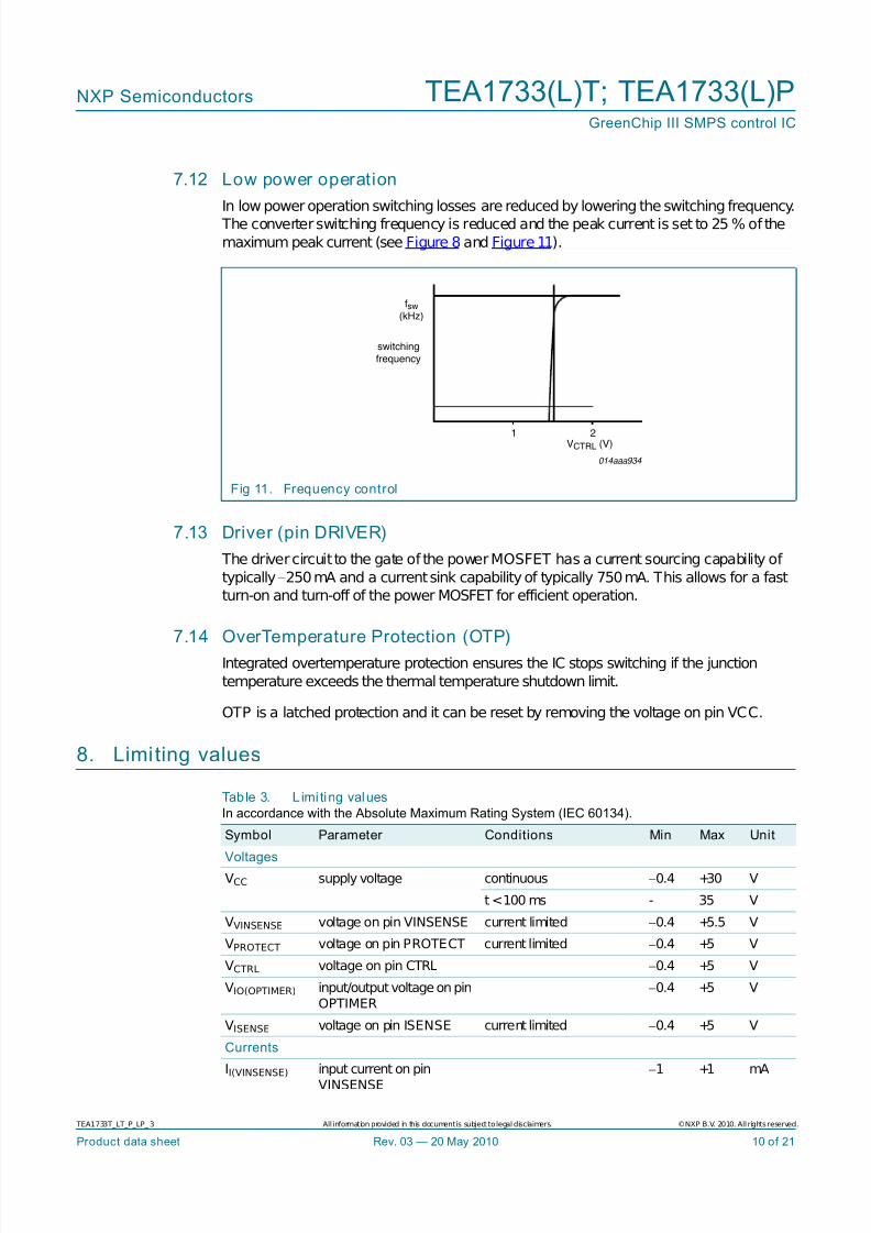
7.12 Low power operation
In low power operation switching losses are reduced by lowering the switching frequency. The converter switching frequency is reduced and the peak current is set to 25 % of the
maximum peak current (see Figure 8 and Figure11).
7.13 Driver (pin DRIVER)
The driver circuit to the gate of the power MOSFET has a current sourcing capability of
typically−250mA and a current sink capability of typically 750mA. This allows for a fastturn-on and turn-off of the power MOSFET for efficient operation.
7.14 OverTemperature Protection (OTP)
Integrated overtemperature protection ensures the IC stops switching if the junction
temperature exceeds the thermal temperature shutdown limit.
OTP is a latched protection and it can be reset by removing the voltage on pin VCC.
8. Limiting values
Fig 11. Frequency control
1 2
switching
frequency
014aaa934
VCTRL (V)
fsw(kHz)
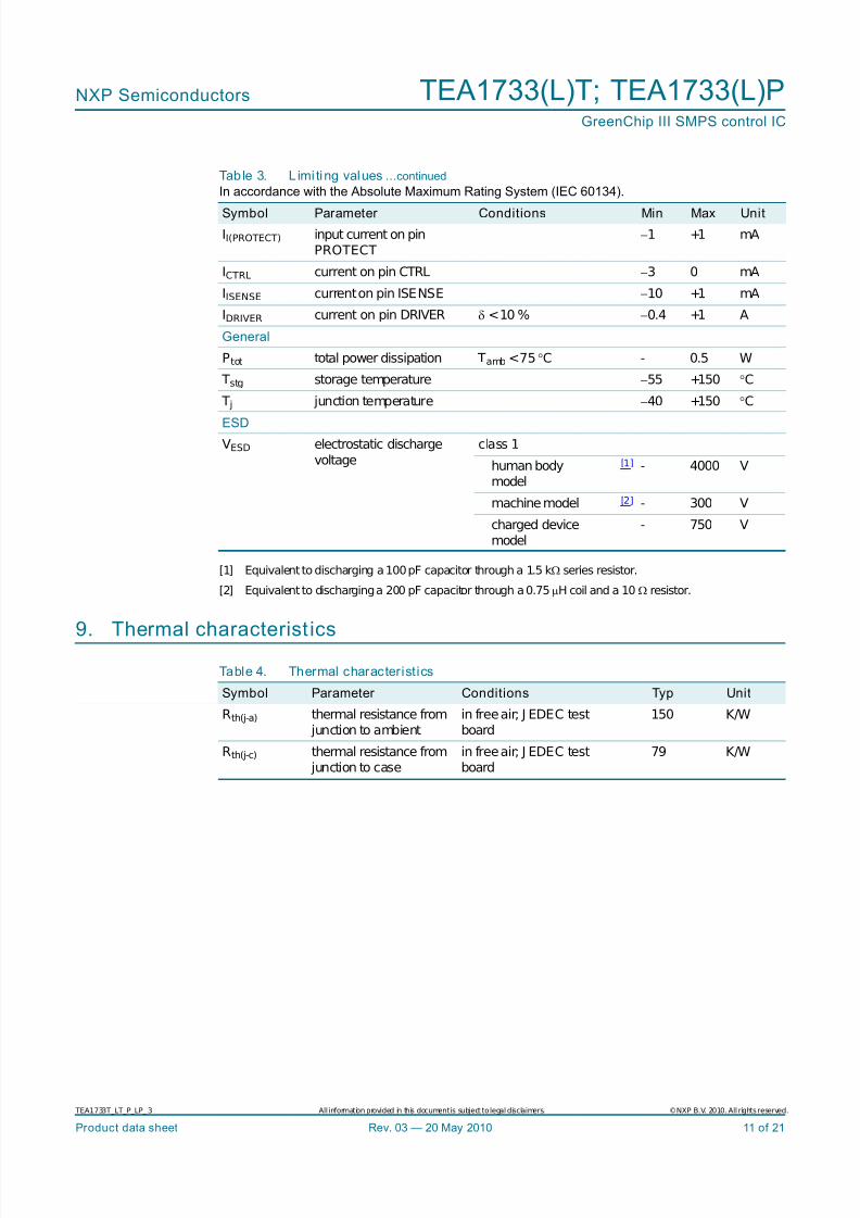
Table 3. L imi ting values
In accordance with the Absolute Maximum Rating System (IEC 60134).
Symbol Parameter Conditions Min Max Unit
Voltages
VCC supply voltage continuous −0.4 +30 V
t <100 ms - 35 V
VVINSENSE voltage on pin VINSENSE current limited −0.4 +5.5 V
VPROTECT voltage on pin PROTECT current limited −0.4 +5 V
VCTRL voltage on pin CTRL −0.4 +5 V
VIO(OPTIMER) input/output voltage on pinOPTIMER
−0.4 +5 V
VISENSE voltage on pin ISENSE current limited −0.4 +5 V
Currents
II(VINSENSE) input current on pin
VINSENSE
−1 +1 mA
7/30/2019 Tea1733t Lt p Lp
http://slidepdf.com/reader/full/tea1733t-lt-p-lp 11/21
TEA1733T_LT_P_LP_ 3 All information provided in this document is subject to legal disclaimers. ©NXP B.V. 2010. All rights reserved.
Product data sheet Rev. 03 — 20 May 2010 11 of 21
NXP Semiconductors TEA1733(L)T; TEA1733(L)PGreenChip III SMPS control IC
[1] Equivalent to discharging a 100pF capacitor through a 1.5 kΩ series resistor.
[2] Equivalent to discharging a 200 pF capacitor through a 0.75μH coil and a 10 Ω resistor.
9. Thermal characterist ics
II(PROTECT) input current on pinPROTECT
−1 +1 mA
ICTRL current on pin CTRL −3 0 mA
IISENSE current on pin ISENSE −10 +1 mA
IDRIVER current on pin DRIVER δ <10 % −0.4 +1 A
General
Ptot total power dissipation Tamb <75 °C - 0.5 W
Tstg storage temperature −55 +150 °C
T j junction temperature −40 +150 °C
ESDVESD electrostatic discharge
voltageclass 1
human bodymodel
[1] - 4000 V
machine model [2] - 300 V
charged devicemodel
- 750 V
Table 3. L imi ting values …continued
In accordance with the Absolute Maximum Rating System (IEC 60134).
Symbol Parameter Conditions Min Max Unit
Table 4. Thermal characteristics
Symbol Parameter Conditions Typ Unit
Rth(j-a) thermal resistance from junction to ambient
in free air; J EDEC testboard
150 K/W
Rth(j-c) thermal resistance from junction to case
in free air; J EDEC testboard
79 K/W
7/30/2019 Tea1733t Lt p Lp
http://slidepdf.com/reader/full/tea1733t-lt-p-lp 12/21
TEA1733T_LT_P_LP_ 3 All information provided in this document is subject to legal disclaimers. ©NXP B.V. 2010. All rights reserved.
Product data sheet Rev. 03 — 20 May 2010 12 of 21
NXP Semiconductors TEA1733(L)T; TEA1733(L)PGreenChip III SMPS control IC
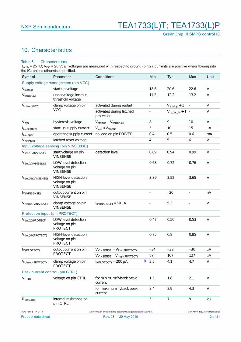
10. Characteristics
Table 5. Character is tics
Tamb = 25 ° C; VCC = 20 V; all voltages are measured with respect to ground (pin 2); currents are positive when flowing into
the IC; unless otherwise specified.
Symbol Parameter Conditions Min Typ Max Unit
Supply voltage management (pin VCC)
Vstartup start-up voltage 18.6 20.6 22.6 V
Vth(UVLO) undervoltage lockoutthreshold voltage
11.2 12.2 13.2 V
Vclamp(VCC) clamp voltage on pinVCC
activated during restart - Vstartup +1 - V
activated during latchedprotection
- Vrst(latch) +1 - V
Vhys hysteresis voltage Vstartup − Vth(UVLO) 8 9 10 V
ICC(startup) start-up supply current VCC <Vstartup 5 10 15 μA
ICC(oper) operating supply current no load on pin DRIVER 0.4 0.5 0.6 mA
Vrst(latch) latched reset voltage 4 5 6 V
Input voltage sensing (pin VINSENSE)
Vstart(VINSENSE) start voltage on pinVINSENSE
detection level 0.89 0.94 0.99 V
Vdet(L)(VINSENSE) LOW-level detectionvoltage on pinVINSENSE
0.68 0.72 0.76 V
Vdet(H)(VINSENSE)
HIGH-level detectionvoltage on pinVINSENSE
3.39 3.52 3.65 V
IO(VINSENSE) output current on pinVINSENSE
- −20 - nA
Vclamp(VINSENSE) clamp voltage on pinVINSENSE
II(VINSENSE) =50μA - 5.2 - V
Protection input (pin PROTECT)
Vdet(L)(PROTECT) LOW-level detectionvoltage on pinPROTECT
0.47 0.50 0.53 V
Vdet(H)(PROTECT) HIGH-level detection
voltage on pinPROTECT
0.75 0.8 0.85 V
IO(PROTECT) output current on pinPROTECT
VVINSENSE =Vlow(PROTECT) −34 −32 −30 μA
VVINSENSE =Vhigh(PROTECT) 87 107 127 μA
Vclamp(PROTECT) clamp voltage on pinPROTECT
II(PROTECT) =200 μA [1] 3.5 4.1 4.7 V
Peak current control (pin CTRL)
VCTRL voltage on pin CTRL for minimum flyback peakcurrent
1.5 1.8 2.1 V
for maximum flyback peakcurrent
3.4 3.9 4.3 V
Rint(CTRL) internal resistance onpin CTRL
5 7 9 kΩ
7/30/2019 Tea1733t Lt p Lp
http://slidepdf.com/reader/full/tea1733t-lt-p-lp 13/21
TEA1733T_LT_P_LP_ 3 All information provided in this document is subject to legal disclaimers. ©NXP B.V. 2010. All rights reserved.
Product data sheet Rev. 03 — 20 May 2010 13 of 21
NXP Semiconductors TEA1733(L)T; TEA1733(L)PGreenChip III SMPS control IC
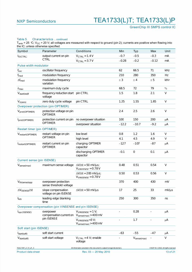
IO(CTRL) output current on pinCTRL
VCTRL =1.4V −0.7 −0.5 −0.3 mA
VCTRL =3.7V −0.28 −0.2 −0.12 mA
Pulse width modulator
f osc oscillator frequency 62 66.5 71 kHz
f mod modulation frequency 210 280 350 Hz
Δf mod modulation frequencyvariation
± 3 ± 4 ± 5 kHz
δmax maximum duty cycle 68.5 72 79 %
Vstart(red)f frequency reduction startvoltage
pin CTRL 1.5 1.8 2.1 V
Vδ(zero) zero duty cycle voltage pin CTRL 1.25 1.55 1.85 V
Overpower protection (pin OPTIMER)
Vprot(OPTIMER) protection voltage on pinOPTIMER
2.4 2.5 2.6 V
Iprot(OPTIMER) protection current on pinOPTIMER
no overpower situation 100 150 200 μA
overpower situation −12.2 −10.7 −9.2 μA
Restart timer (pin OPTIMER)
Vrestart(OPTIMER) restart voltage on pinOPTIMER
low level 0.8 1.2 1.6 V
high level 4.1 4.5 4.9 V
Irestart(OPTIMER) restart current on pinOPTIMER
charging OPTIMERcapacitor
−127 −107 −87 μA
discharging OPTIMERcapacitor
−0.1 0 0.1 μA
Current sense (pin ISENSE)
Vsense(max) maximum sense voltage ΔV/Δt =50 mV/μs;VVINSENSE =0.78V
0.48 0.51 0.54 V
ΔV/Δt =200 mV/μs;VVINSENSE =0.78V
0.50 0.53 0.56 V
Vth(sense)opp overpower protectionsense threshold voltage
370 400 430 mV
ΔVISENSE/Δt slope compensationvoltage on pin ISENSE
ΔV/Δt =50 mV/μs 17 25 33 mV/μs
tleb leading edge blankingtime
250 300 350 ns
Overpower compensation (pin VINSENSE and pin ISENSE)
Iopc(ISENSE) overpowercompensation current onpin ISENSE
VVINSENSE =1 V;Vsense(max)>400mV
- 0.28 - μA
VVINSENSE=3 V;Vsense(max)>400mV
- 1.7 - μA
Soft start (pin ISENSE)
Istart(soft) soft start current −63 −55 −47 μA
Vstart(soft) soft start voltage VCTRL =4 V; enablevoltage
- Vsense(max) - V
Table 5. Character is tics …continued
Tamb = 25 ° C; VCC = 20 V; all voltages are measured with respect to ground (pin 2); currents are positive when flowing into
the IC; unless otherwise specified.Symbol Parameter Conditions Min Typ Max Unit
7/30/2019 Tea1733t Lt p Lp
http://slidepdf.com/reader/full/tea1733t-lt-p-lp 14/21
TEA1733T_LT_P_LP_ 3 All information provided in this document is subject to legal disclaimers. ©NXP B.V. 2010. All rights reserved.
Product data sheet Rev. 03 — 20 May 2010 14 of 21
NXP Semiconductors TEA1733(L)T; TEA1733(L)PGreenChip III SMPS control IC
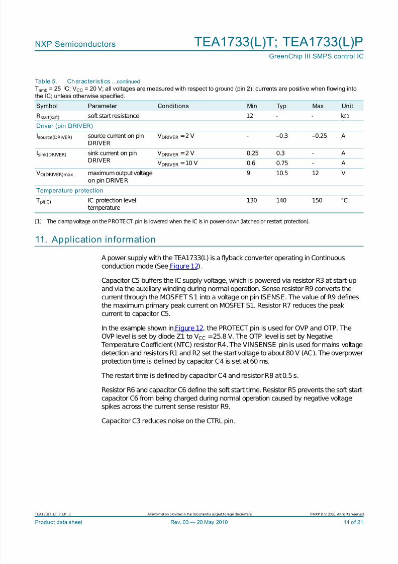
[1] The clamp voltage on the PROTECT pin is lowered when the IC is in power-down (latched or restart protection).
11. Application information
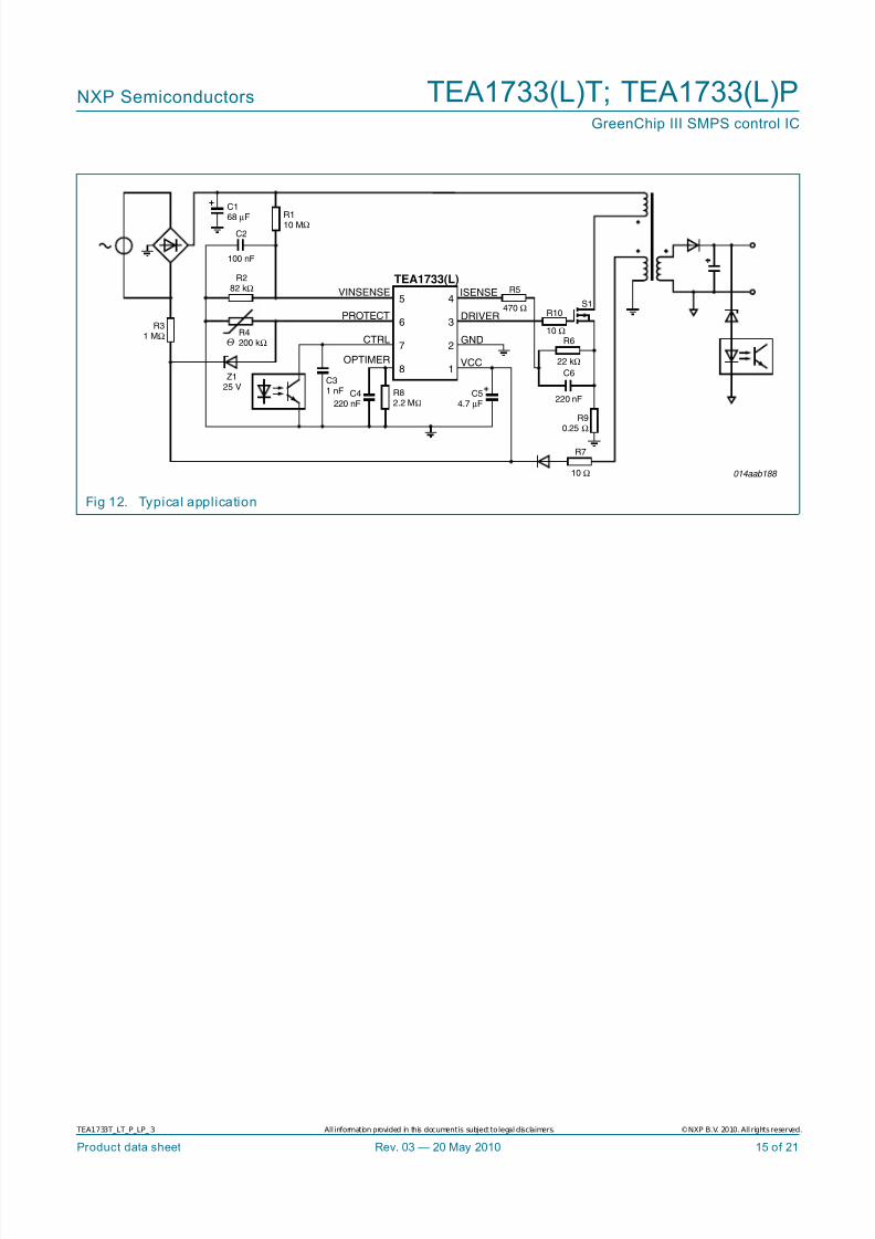
A power supply with the TEA1733(L) is a flyback converter operating in Continuous
conduction mode (See Figure12).
Capacitor C5 buffers the IC supply voltage, which is powered via resistor R3 at start-upand via the auxiliary winding during normal operation. Sense resistor R9 converts the
current through the MOSFET S1 into a voltage on pin ISENSE. The value of R9 definesthe maximum primary peak current on MOSFET S1. Resistor R7 reduces the peakcurrent to capacitor C5.
In the example shown in Figure12, the PROTECT pin is used for OVP and OTP. TheOVP level is set by diode Z1 to VCC =25.8 V. The OTP level is set by Negative
Temperature Coefficient (NTC) resistor R4. The VINSENSE pin is used for mains voltage
detection and resistors R1 and R2 set the start voltage to about 80 V (AC). The overpowerprotection time is defined by capacitor C4 is set at 60 ms.
The restart time is defined by capacitor C4 and resistor R8 at 0.5s.
Resistor R6 and capacitor C6 define the soft start time. Resistor R5 prevents the soft start
capacitor C6 from being charged during normal operation caused by negative voltagespikes across the current sense resistor R9.
Capacitor C3 reduces noise on the CTRL pin.
Rstart(soft) soft start resistance 12 - - kΩ
Driver (pin DRIVER)
Isource(DRIVER) source current on pinDRIVER
VDRIVER =2 V - −0.3 −0.25 A
Isink(DRIVER) sink current on pinDRIVER
VDRIVER =2 V 0.25 0.3 - A
VDRIVER =10 V 0.6 0.75 - A
VO(DRIVER)max maximum output voltageon pin DRIVER
9 10.5 12 V
Temperature protection
Tpl(IC) IC protection leveltemperature
130 140 150 °C
Table 5. Character is tics …continued
Tamb = 25 ° C; VCC = 20 V; all voltages are measured with respect to ground (pin 2); currents are positive when flowing into
the IC; unless otherwise specified.Symbol Parameter Conditions Min Typ Max Unit
7/30/2019 Tea1733t Lt p Lp
http://slidepdf.com/reader/full/tea1733t-lt-p-lp 15/21
TEA1733T_LT_P_LP_ 3 All information provided in this document is subject to legal disclaimers. ©NXP B.V. 2010. All rights reserved.
Product data sheet Rev. 03 — 20 May 2010 15 of 21
NXP Semiconductors TEA1733(L)T; TEA1733(L)PGreenChip III SMPS control IC
Fig 12. Typical application
014aab188
TEA1733(L)
5
6
7
8
4
3
2
1
R110 MΩ
R282 kΩ
R31 MΩ R4
200 kΩ
Z125 V
C4220 nF
R82.2 MΩ
C54.7 μF
R90.25 Ω
C31 nF
C1
68 μF
C2
100 nF
R7
10 Ω
220 nF
C6
22 kΩ
R610 Ω
R10S1
R5
Θ
DRIVER
GND
VCC
ISENSEVINSENSE
PROTECT
CTRL
OPTIMER
470 Ω
7/30/2019 Tea1733t Lt p Lp
http://slidepdf.com/reader/full/tea1733t-lt-p-lp 16/21
TEA1733T_LT_P_LP_ 3 All information provided in this document is subject to legal disclaimers. ©NXP B.V. 2010. All rights reserved.
Product data sheet Rev. 03 — 20 May 2010 16 of 21
NXP Semiconductors TEA1733(L)T; TEA1733(L)PGreenChip III SMPS control IC
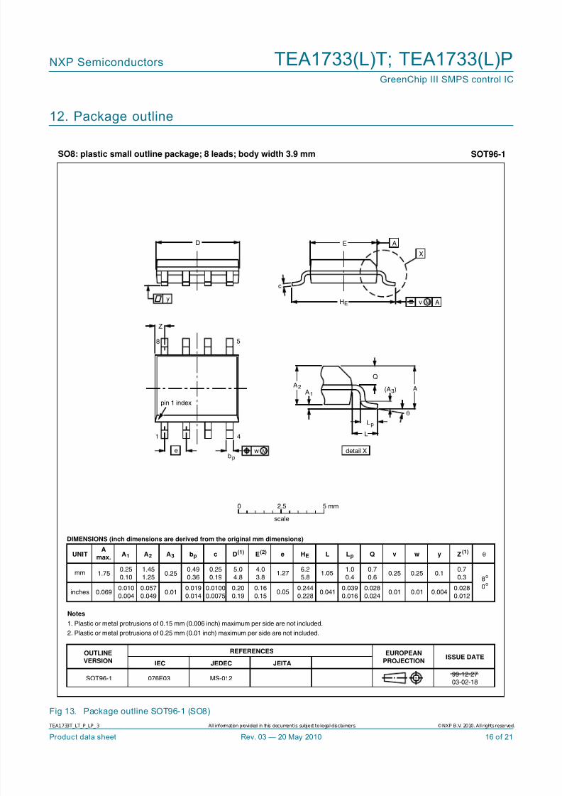
12. Package outline
Fig 13. Package outline SOT96-1 (SO8)
UNITA
max.A
1A
2A
3b
pc D(1) E(2) (1)e H
EL L
pQ Zywv θ
REFERENCESOUTLINE
VERSION
EUROPEAN
PROJECTIONISSUE DATE
IEC JEDEC JEITA
mm
inches
1.750.25
0.10
1.45
1.250.25
0.49
0.36
0.25
0.19
5.0
4.8
4.0
3.81.27
6.2
5.81.05
0.7
0.6
0.7
0.3 8
0
o
o
0.25 0.10.25
DIMENSIONS (inch dimensions are derived from the original mm dimensions)
Notes
1. Plastic or metal protrusions of 0.15 mm (0.006 inch) maximum per side are not included.
2. Plastic or metal protrusions of 0.25 mm (0.01 inch) maximum per side are not included.
1.0
0.4
SOT96-1
X
w M
θ
AA1
A2
bp
D
HE
Lp
Q
detail X
E
Z
e
c
L
v M A
(A )3
A
4
5
pin 1 index
1
8
y
076E03 MS-012
0.0690.010
0.004
0.057
0.0490.01
0.019
0.014
0.0100
0.0075
0.20
0.19
0.16
0.150.05
0.244
0.228
0.028
0.024
0.028
0.0120.010.010.041 0.004
0.039
0.016
0 2.5 5 mm
scale
SO8: plastic small outline package; 8 leads; body width 3.9 mm SOT96-1
99-12-27
03-02-18
7/30/2019 Tea1733t Lt p Lp
http://slidepdf.com/reader/full/tea1733t-lt-p-lp 17/21
TEA1733T_LT_P_LP_ 3 All information provided in this document is subject to legal disclaimers. ©NXP B.V. 2010. All rights reserved.
Product data sheet Rev. 03 — 20 May 2010 17 of 21
NXP Semiconductors TEA1733(L)T; TEA1733(L)PGreenChip III SMPS control IC
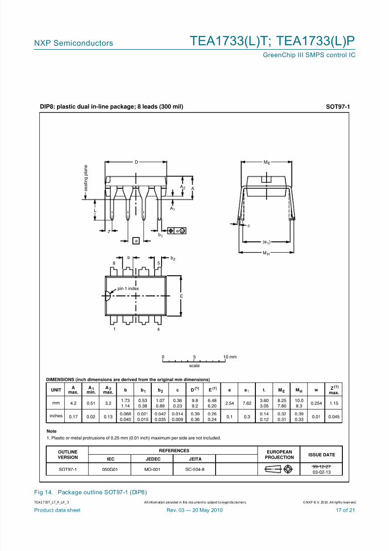
Fig 14. Package outline SOT97-1 (DIP8)
REFERENCESOUTLINE
VERSION
EUROPEAN
PROJECTIONISSUE DATE
IEC JEDEC JEITA
SOT97-199-12-27
03-02-13
UNIT Amax.
1 2 b1(1) (1) (1)
b2 c D E e M ZHL
mm
DIMENSIONS (inch dimensions are derived from the original mm dimensions)
Amin.
Amax.
bmax.
wMEe1
1.73
1.14
0.53
0.38
0.36
0.23
9.8
9.2
6.48
6.20
3.60
3.050.2542.54 7.62
8.25
7.80
10.0
8.31.154.2 0.51 3.2
inches 0.068
0.045
0.021
0.015
0.014
0.009
1.07
0.89
0.042
0.035
0.39
0.36
0.26
0.24
0.14
0.120.010.1 0.3
0.32
0.31
0.39
0.330.0450.17 0.02 0.13
b2
050G01 MO-001 SC-504-8
MH
c
(e )1
ME
A
L
s e a t i n g
p l a n e
A1
w Mb1
e
D
A2
Z
8
1
5
4
b
E
0 5 10 mm
scale
Note
1. Plastic or metal protrusions of 0.25 mm (0.01 inch) maximum per side are not included.
pin 1 index
DIP8: plastic dual in-line package; 8 leads (300 mil) SOT97-1
7/30/2019 Tea1733t Lt p Lp
http://slidepdf.com/reader/full/tea1733t-lt-p-lp 18/21
TEA1733T_LT_P_LP_ 3 All information provided in this document is subject to legal disclaimers. ©NXP B.V. 2010. All rights reserved.
Product data sheet Rev. 03 — 20 May 2010 18 of 21
NXP Semiconductors TEA1733(L)T; TEA1733(L)PGreenChip III SMPS control IC
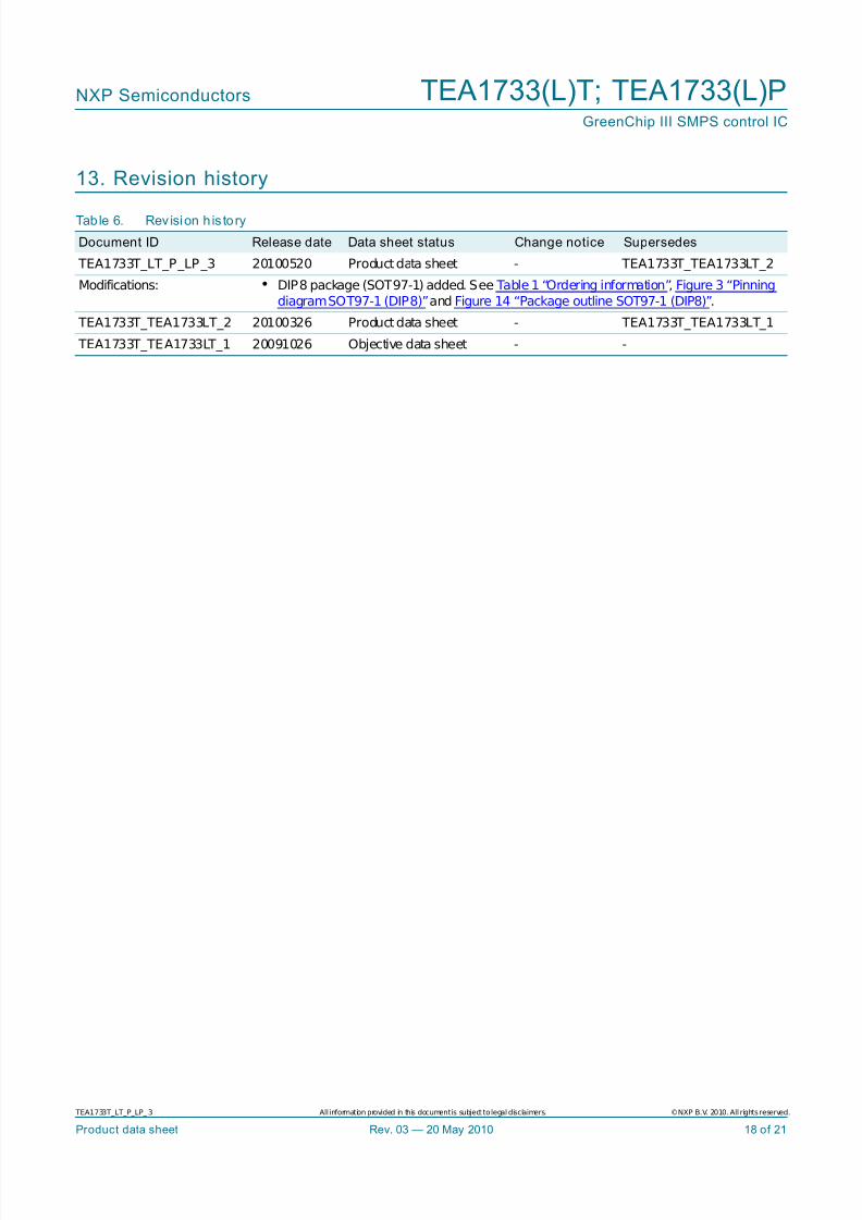
13. Revision history
Table 6. Rev ision h is tory
Document ID Release date Data sheet status Change notice Supersedes
TEA1733T_LT_P_LP_3 20100520 Product data sheet - TEA1733T_TEA1733LT_2
Modifications: • DIP8 package (SOT97-1) added. See Table 1 “Ordering information”, Figure 3 “Pinningdiagram SOT97-1 (DIP8)”and Figure 14 “Package outline SOT97-1 (DIP8)”.
TEA1733T_TEA1733LT_2 20100326 Product data sheet - TEA1733T_TEA1733LT_1
TEA1733T_TEA1733LT_1 20091026 Objective data sheet - -
7/30/2019 Tea1733t Lt p Lp
http://slidepdf.com/reader/full/tea1733t-lt-p-lp 19/21
TEA1733T_LT_P_LP_ 3 All information provided in this document is subject to legal disclaimers. ©NXP B.V. 2010. All rights reserved.
Product data sheet Rev. 03 — 20 May 2010 19 of 21
NXP Semiconductors TEA1733(L)T; TEA1733(L)PGreenChip III SMPS control IC
14. Legal information
14.1 Data sheet status
[1] Please consult the most recently issued document before initiating or completing a design.
[2] The term ‘short data sheet’ is explained in section “Definitions”.
[3] The product status of device(s) described in this document may have changed since this document was published and may differ in case of multiple devices. The latest product statusinformation is available on the Internet at URL http://www.nxp.com.
14.2 DefinitionsDraft — The document is a draft version only. The content is still under
internal review and subject to formal approval, which may result in
modifications or additions. NXP Semiconductors does not give any
representations or warranties as to the accuracy or completeness of
information included herein and shall have no liability for the consequences of
use of such information.
Short data sheet — A short data sheet is an extract from a full data sheet
with the same product type number(s) and title. A short data sheet is intended
for quick reference only and should not be relied upon to contain detailed and
full information. For detailed and full information see the relevant full data
sheet, which is available on request via the local NXP Semiconductors sales
office. In case of any inconsistency or conflict with the short data sheet, the
full data sheet shall prevail.
Product specification — The information and data provided in a Product
data sheet shall define the specification of the product as agreed between
NXP Semiconductors and its customer, unless NXP Semiconductors and
customer have explicitly agreed otherwise in writing. In no event however,
shall an agreement be valid in which the NXP Semiconductors product is
deemed to offer functions and qualities beyond those described in the
Product data sheet.
14.3 Disclaimers
Limited warranty and liability — Information in this document is believed to
be accurate and reliable. However, NXP Semiconductors does not give any
representations or warranties, expressed or implied, as to the accuracy or
completeness of such information and shall have no liability for the
consequences of use of such information.
In no event shall NXP Semiconductors be liable for any indirect, incidental,
punitive, special or consequential damages (including - without limitation - lost
profits, lost savings, business interruption, costs related to the removal or
replacement of any products or rework charges) whether or not such
damages are based on tort (including negligence), warranty, breach of
contract or any other legal theory.
Notwithstanding any damages that customer might incur for any reason
whatsoever, NXP Semiconductors’ aggregate and cumulative liability towards
customer for the products described herein shall be limited in accordance
with the Terms and conditions of commercial sale of NXP Semiconductors.
Right to m ake changes — NXP Semiconductors reserves the right to make
changes to information published in this document, including without
limitation specifications and product descriptions, at any time and without
notice. This document supersedes and replaces all information supplied prior
to the publication hereof.
Suitability for use — NXP Semiconductors products are not designed,
authorized or warranted to be suitable for use in life support, life-critical orsafety-critical systems or equipment, nor in applications where failure or
malfunction of an NXP Semiconductors product can reasonably be expected
to result in personal injury, death or severe property or environmental
damage. NXP Semiconductors accepts no liability for inclusion and/or use of
NXP Semiconductors products in such equipment or applications and
therefore such inclusion and/or use is at the customer’s own risk.
Appli cati ons — Applications that are described herein for any of these
products are for illustrative purposes only. NXP Semiconductors makes no
representation or warranty that such applications will be suitable for the
specified use without further testing or modification.
Customers are responsible for the design and operation of their applications
and products using NXP Semiconductors products, and NXP Semiconductors
accepts no liability for any assistance with applications or customer product
design. It is customer’s sole responsibility to determine whether the NXP
Semiconductors product is suitable and fit for the customer’s applications and
products planned, as well as for the planned application and use of
customer’s third party customer(s). Customers should provide appropriate
design and operating safeguards to minimize the risks associated with theirapplications and products.
NXP Semiconductors does not accept any liability related to any default,
damage, costs or problem which is based on any weakness or default in the
customer’s applications or products, or the application or use by customer’s
third party customer(s). Customer is responsible for doing all necessary
testing for the customer’s applications and products using NXP
Semiconductors products in order to avoid a default of the applications and
the products or of the application or use by customer’s third party
customer(s). NXP does not accept any liability in this respect.
Limiting values — Stress above one or more limiting values (as defined in
the Absolute Maximum Ratings System of IEC 60134) will cause permanent
damage to the device. Limiting values are stress ratings only and (proper)
operation of the device at these or any other conditions above those given in
the Recommended operating conditions section (if present) or the
Characteristics sections of this document is not warranted. Constant or
repeated exposure to limiting values will permanently and irreversibly affectthe quality and reliability of the device.
Terms and condition s of com mercial sale — NXP Semiconductors
products are sold subject to the general terms and conditions of commercial
sale, as published at http://www.nxp.com/profile/terms , unless otherwise
agreed in a valid written individual agreement. In case an individual
agreement is concluded only the terms and conditions of the respective
agreement shall apply. NXP Semiconductors hereby expressly objects to
applying the customer’s general terms and conditions with regard to the
purchase of NXP Semiconductors products by customer.
No offer to sell or license — Nothing in this document may be interpreted or
construed as an offer to sell products that is open for acceptance or the grant,
conveyance or implication of any license under any copyrights, patents or
other industrial or intellectual property rights.
Export control — This document as well as the item(s) described herein
may be subject to export control regulations. Export might require a priorauthorization from national authorities.
Document status[1][2] Product status[3] Definition
Objective [short] data sheet Development This document contains data from the objective specification for product development.
Preliminary [short] data sheet Qualification This document contains data from the preliminary specification.
Product [short] data sheet Production This document contains the product specification.
7/30/2019 Tea1733t Lt p Lp
http://slidepdf.com/reader/full/tea1733t-lt-p-lp 20/21
TEA1733T_LT_P_LP_ 3 All information provided in this document is subject to legal disclaimers. ©NXP B.V. 2010. All rights reserved.
Product data sheet Rev. 03 — 20 May 2010 20 of 21
NXP Semiconductors TEA1733(L)T; TEA1733(L)PGreenChip III SMPS control IC
Non-automotive qualified pro ducts — Unless this data sheet expressly
states that this specific NXP Semiconductors product is automotive qualified,
the product is not suitable for automotive use. It is neither qualified nor tested
in accordance with automotive testing or application requirements. NXPSemiconductors accepts no liability for inclusion and/or use of
non-automotive qualified products in automotive equipment or applications.
In the event that customer uses the product for design-in and use in
automotive applications to automotive specifications and standards, customer
(a) shall use the product without NXP Semiconductors’ warranty of the
product for such automotive applications, use and specifications, and (b)
whenever customer uses the product for automotive applications beyond
NXP Semiconductors’ specifications such use shall be solely at customer’s
own risk, and (c) customer fully indemnifies NXP Semiconductors for any
liability, damages or failed product claims resulting from customer design and
use of the product for automotive applications beyond NXP Semiconductors’
standard warranty and NXP Semiconductors’ product specifications.
14.4 Trademarks
Notice: All referenced brands, product names, service names and trademarks
are the property of their respective owners.
GreenChip — is a trademark of NXP B.V.
15. Contact information
For more information, please visit: http://www.nxp.com
For sales office addresses, please send an email to: [email protected]
7/30/2019 Tea1733t Lt p Lp
http://slidepdf.com/reader/full/tea1733t-lt-p-lp 21/21
NXP Semiconductors TEA1733(L)T; TEA1733(L)PGreenChip III SMPS control IC
© NXP B.V. 2010. All rights reserved.For more information, please visit: http://www.nxp.comFor sales office addresses, please send an email to: [email protected]
Date of release: 20 May 2010
Document identifier: TEA1733T_LT_P_LP_3
Please be aware that important notices concerning this document and the product(s)described herein, have been included in section ‘Legal information’.
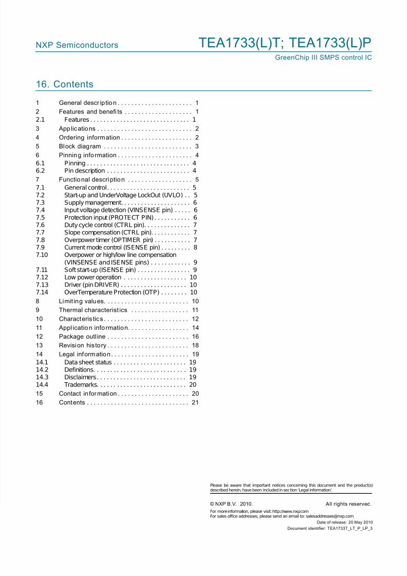
16. Contents
1 General descr iption . . . . . . . . . . . . . . . . . . . . . . 1
2 Features and benefi ts . . . . . . . . . . . . . . . . . . . . 1
2.1 Features . . . . . . . . . . . . . . . . . . . . . . . . . . . . . . 1
3 App lications . . . . . . . . . . . . . . . . . . . . . . . . . . . . 2
4 Ordering information . . . . . . . . . . . . . . . . . . . . . 2
5 Block diagram . . . . . . . . . . . . . . . . . . . . . . . . . . 3
6 Pinning info rmation . . . . . . . . . . . . . . . . . . . . . . 4
6.1 Pinning . . . . . . . . . . . . . . . . . . . . . . . . . . . . . . . 46.2 Pin description . . . . . . . . . . . . . . . . . . . . . . . . . 4
7 Functional description . . . . . . . . . . . . . . . . . . . 5
7.1 General control. . . . . . . . . . . . . . . . . . . . . . . . . 57.2 Start-up and UnderVoltage LockOut (UVLO) . . 5
7.3 Supply management. . . . . . . . . . . . . . . . . . . . . 67.4 Input voltage detection (VINSENSE pin) . . . . . 67.5 Protection input (PROTECT PIN) . . . . . . . . . . . 67.6 Duty cycle control (CTRL pin). . . . . . . . . . . . . . 77.7 Slope compensation (CTRL pin). . . . . . . . . . . . 77.8 Overpower timer (OPTIMER pin) . . . . . . . . . . . 77.9 Current mode control (ISENSE pin) . . . . . . . . . 87.10 Overpower or high/low line compensation
(VINSENSE and ISENSE pins) . . . . . . . . . . . . 97.11 Soft start-up (ISENSE pin) . . . . . . . . . . . . . . . . 97.12 Low power operation . . . . . . . . . . . . . . . . . . . 107.13 Driver (pin DRIVER) . . . . . . . . . . . . . . . . . . . . 107.14 OverTemperature Protection (OTP) . . . . . . . . 10
8 Limit ing values. . . . . . . . . . . . . . . . . . . . . . . . . 109 Thermal characterist ics . . . . . . . . . . . . . . . . . 11
10 Characteris tics . . . . . . . . . . . . . . . . . . . . . . . . . 12
11 Appl ication info rmation. . . . . . . . . . . . . . . . . . 14
12 Package outl ine . . . . . . . . . . . . . . . . . . . . . . . . 16
13 Revision his tory . . . . . . . . . . . . . . . . . . . . . . . . 18
14 Legal information. . . . . . . . . . . . . . . . . . . . . . . 19
14.1 Data sheet status . . . . . . . . . . . . . . . . . . . . . . 1914.2 Definitions. . . . . . . . . . . . . . . . . . . . . . . . . . . . 1914.3 Disclaimers. . . . . . . . . . . . . . . . . . . . . . . . . . . 1914.4 Trademarks. . . . . . . . . . . . . . . . . . . . . . . . . . . 20
15 Contact information . . . . . . . . . . . . . . . . . . . . . 20
16 Contents . . . . . . . . . . . . . . . . . . . . . . . . . . . . . . 21
Recommended