Application ReportSPMA036B–September 2011–Revised February 2013
System Design Guidelines for Stellaris® MicrocontrollersJonathan Guy ............................................................................................... Stellaris® Microcontrollers
ABSTRACT
Stellaris® LM3S and LM4F microcontrollers are highly-integrated system-on-chip (SOC) devices withextensive interface and processing capabilities. Consequently, there are many factors to consider whencreating a schematic and designing a circuit board. By following the recommendations in this designguide, you will increase your confidence that the board will work the first time it is powered it up.
Contents1 Introduction .................................................................................................................. 22 Using This Guide ............................................................................................................ 23 General Design Information ............................................................................................... 24 Feature-Specific Design Information .................................................................................... 115 PCB Layout Examples .................................................................................................... 216 System Design Examples ................................................................................................ 237 Conclusion .................................................................................................................. 238 References ................................................................................................................. 23
List of Figures
1 PCB Routing Options....................................................................................................... 5
2 Comparing Oscillator Circuits in LM4F and LM3S Devices ........................................................... 7
3 Recommended Layout for Small Surface-Mount Crystal .............................................................. 8
4 Acceptable PCB Trace Routing ......................................................................................... 10
5 Typical Four-Layer PCB Stack with Routing Assignments........................................................... 12
6 Transmission Lines for Ethernet Signaling............................................................................. 13
7 100-Ω Microstrip Differential Pair on a Four-Layer, 0.06-in FR-4 PCB Stack ..................................... 13
8 Chassis Ground Guidelines .............................................................................................. 16
9 Typical Four-Layer PCB Stack .......................................................................................... 17
10 90-Ω Microstrip Differential Pair on a Four-Layer, 0.06-in FR-4 PCB Stack....................................... 17
11 Examples of PCB Trace Layout ......................................................................................... 19
12 Examples of Differential Pair Layout .................................................................................... 19
13 Stellaris LM3S9B90 Microcontroller Minimal Circuit .................................................................. 21
14 Stellaris LM3S811 Microcontroller Minimal Circuit .................................................................... 22
Stellaris, StellarisWare are registered trademarks of Texas Instruments.ARM is a registered trademark of ARM Limited.All other trademarks are the property of their respective owners.
1SPMA036B–September 2011–Revised February 2013 System Design Guidelines for Stellaris® MicrocontrollersSubmit Documentation Feedback
Copyright © 2011–2013, Texas Instruments Incorporated

Introduction www.ti.com
1 Introduction
The General Design Information section of this guide contains design information that applies to mostdesigns (Section 3). Topics include important factors in the schematic design and layout of powersupplies, oscillators, and debug accessibility. The Feature-Specific Design Information section describesspecific peripherals and their unique considerations, allowing you to select the information that is relevantto your design (Section 4).
To further assist you with the design process, Texas Instruments provides a wide range of additionaldesign resources, including application reports and reference designs. These designs and documents arean important reference. See the System Design Examples (Section 6) for links to these resources.
2 Using This Guide
The information in this design guide is intended to be general enough to cover a wide range of designs bydescribing solutions for typical situations. However, because every system is different, it is inevitable thatthere will be conflicting requirements and potential trade-offs. This is especially true in designs that includehigh-performance analog circuits, radio frequencies, high voltages, or high currents. If your designincludes these features, then special considerations (beyond the scope of this application report) may benecessary.
Where possible, the distinction is made between preferred practice and acceptable practice. Thisdistinction addresses the reality that constraints such as size, cost, and layout restrictions might notalways allow for best-practice design.
When considering which practices to apply to a design, one of the most important factors is the I/Oswitching rate and current. If there is only low-speed, low-current switching on the Stellaris peripheral pins,then acceptable-practice rules are likely sufficient. If high-speed switching is present, particularly withsimultaneous transitions (for example, the EPI module), then best-practice rules are recommended.
NOTE: Some of the information in this guide comes directly from the individual Stellarismicrocontroller data sheets. The microcontroller data sheets are the defining documents fordevice usage and may contain specific requirements that are not covered in this designguide. You should always use the most current version of the data sheet and also check themost recent errata documents for the part number you have selected. Visitwww.ti.com/stellaris to sign up for e-mail alerts specific to a Stellaris part number.
3 General Design Information
This section contains design information that applies to most Stellaris microcontrollers including:
• Power
• Reset
• Oscillators
• JTAG Interface
• System
• All External Signals
2 System Design Guidelines for Stellaris® Microcontrollers SPMA036B–September 2011–Revised February 2013Submit Documentation Feedback
Copyright © 2011–2013, Texas Instruments Incorporated
www.ti.com General Design Information
3.1 Power
This section describes design considerations related to the microcontroller power supply.
3.1.1 Microcontroller Power Supply
Description Classification Applies to... For more information, see...
Stellaris microcontroller power supply Schematic All Stellaris Microcontroller data sheetrequirements recommendations microcontrollers
Stellaris microcontrollers require only a single +3.3-V power supply. Other supply rails are generatedinternally by on-chip, low drop-out (LDO) regulators. The most visible internal supply rail is the corevoltage (VDDC or VDD25) because it has dedicated power pins for filter and decoupling capacitors.
Some Stellaris microcontrollers allow VDDC to be provided from an external power source; see the PowerControl section of the System Control chapter in the respective data sheet to determine if a specificdevice allows an external regulator. In certain applications, a designer might wish to use a switchingpower supply to reduce power loss in the VDDC supply. A typical switching regulator has an efficiency of85% compared to 36% for a 1.2-V linear regulator operating from 3.3 V.
The easiest way to avoid potential power sequencing issues when using a VDDC switching supply is to useVDD (+3.3 V) as the switcher input source. For specific sequencing requirements, see the correspondingmicrocontroller data sheet.
If an external VDDC source is used, the on-chip LDO regulator must still have a filter capacitor on its output.See Section 3.1.2, LDO Filter Capacitor, for details.
An external linear regulator offers no advantage over the on-chip linear regulator other than a smallreduction in power dissipation within the Stellaris microcontroller.
During normal microcontroller operation, the power-supply rail must remain within the electrical limits listedin the microcontroller data sheet [VDD (min) and VDD (max)]. For optimal performance of the on-chip analogmodules, the supply rail should be well regulated and have minimal ripple. Electrical noise sources suchas motor drivers, relays, and other power-switching circuits should each have a separate supply rail,especially if analog-to-digital converter (ADC) performance is a factor.
The microcontroller internal power-on reset (POR) circuit releases once the VDD power-supply rail reachesthe POR threshold Vth. The brown-out reset (BOR) circuit is a more precise supply rail monitor and isnormally used to hold the microcontroller in reset if the supply rail drops out of operating range. On someStellaris devices, the default BOR action is to generate a system reset. However, on other Stellarisdevices, the software must configure the BOR to generate a reset rather than an interrupt. Use of theBOR function is highly recommended.
External supervisors may also be used to assert the external reset signal RSTn under power-on, brown-out, or watchdog expiration conditions.
3SPMA036B–September 2011–Revised February 2013 System Design Guidelines for Stellaris® MicrocontrollersSubmit Documentation Feedback
Copyright © 2011–2013, Texas Instruments Incorporated

General Design Information www.ti.com
3.1.2 LDO Filter Capacitor
Description Classification Applies to... For more information, see...
Information on selecting the right Schematic All Stellariscapacitor for the on-chip LDO voltage Microcontroller data sheetrecommendations microcontrollersregulator
All Stellaris microcontrollers have an on-chip voltage regulator to provide power to the core. On mostparts, the LDO output must be connected to the VDDC power pins. The voltage regulator requires a filtercapacitor to operate properly (see the CLDO parameter in the corresponding microcontroller data sheet foracceptable capacitor values).
The LDO capacitance is the sum of capacitor values on the LDO and VDDC pins. Typically, the LDO pincapacitor is 1 μF to 2.2 μF with additional 0.1-μF capacitors distributed on the VDDC pins. Use of capacitorsoutside of the CLDO range might prevent the regulator from starting or achieving regulation.
The recommended main LDO capacitor for LM3S series microcontrollers is 2.2 μF, 10 V to 25 V,X5R/X7R with 20% tolerance or better. The recommended VDDC capacitor solution consists of two or more10%-tolerance ceramic chip capacitors totalling 3.3 μF to 3.4 μF (that is, one each of 3.3-μF and 0.1-μFcapacitors). Z5U dielectric capacitors are not recommended due to wide tolerance over temperature.
If an external VDDC source is used, the on-chip LDO regulator must continue to have a filter capacitor on itsoutput. The filter capacitance must be within the specified range to maintain regulator stability even thoughits output is otherwise not connected.
3.1.3 Decoupling Capacitors
Description Classification Applies to... For more information, see...
Information on selecting the right Schematic All Stellaris Microcontroller data sheetpower-rail decoupling capacitors recommendations microcontrollers
Ideally, Stellaris microcontrollers should have one decoupling capacitor in close proximity to each power-supply pin. Decoupling capacitors are typically 0.01 μF or 0.1 μF in value and should be accompanied bya bulk capacitor near the microcontroller. The combined VDD and VDDA bulk capacitance of themicrocontroller is typically between 2 μF and 22 μF, with values on the upper end of that range providingmeasurable ripple reduction in some applications, especially if the circuit board does not have solid powerand ground planes. Bulk capacitance is particularly important if the microcontroller is connected to high-speed interfaces or needs to source significant GPIO current (that is, greater than 4 mA) on more than afew pins.
For optimal performance, locate one decoupling capacitor adjacent to each Power and Ground pin pair. Ata minimum, there should be one decoupling capacitor on each side of the microcontroller package. VDDC
pins should always have an adjacent decoupling capacitor.
Decoupling capacitors should be 10 V to 25 V, X5R/X7R ceramic chip types. Z5U dielectric capacitors arenot recommended due to wide tolerance over temperature.
The capacitance of most ceramic capacitors decreases with increasing voltage. Avoid using capacitors atclose to their rated voltage unless reduced capacitance is acceptable. X7R capacitors may lose 15%-20%of their capacitance at rated voltage while Y5V capacitors may drop 75%-80%. [(Cain, Jeffrey,Comparison of Multilayer Ceramic and Tantalum Capacitors, AVX Technical Bulletin.)]
Description Classification Applies to... For more information, see...
Optimal layout practices when placing Layout All Stellarisand routing power vias and Microcontroller data sheetrecommendations microcontrollersdecoupling capacitors
4 System Design Guidelines for Stellaris® Microcontrollers SPMA036B–September 2011–Revised February 2013Submit Documentation Feedback
Copyright © 2011–2013, Texas Instruments Incorporated

Cap
Cap
Cap
VD
D
GN
D
Cap
VD
D
GN
D
Cap
VD
D
GN
D
Cap
VD
D
GN
D
Best practice
Minimal inductance from
between capacitor, pins and
power planes.
Not recommended
Distance from pins to vias
increases inductance in
power rails.
Acceptable
Inductance to VDD and
GND planes is minimized.
Acceptable
Although GND trace from
the pin to capacitor is not
optimal, the inductance from
pins to power places is low.
Not recommended
Via is located too far from
GND pin, adding inductance
to the path.
Acceptable
Via locations are as close to
pins as possible. Traces to
capacitor are as short as
practical.
www.ti.com General Design Information
Figure 1 show different options for routing PCB traces between the Stellaris microcontroller power pinsand a decoupling capacitor.
Figure 1. PCB Routing Options
5SPMA036B–September 2011–Revised February 2013 System Design Guidelines for Stellaris® MicrocontrollersSubmit Documentation Feedback
Copyright © 2011–2013, Texas Instruments Incorporated

General Design Information www.ti.com
3.1.4 Splitting Power Rails and Grounds
Description Classification Applies to... For more information, see...
Factors to consider when deciding Schematic All Stellarishow to connect VDD, VDDA, GND, and Microcontroller data sheetrecommendations microcontrollersGNDA pins
Stellaris microcontrollers are designed to operate with VDD and VDDA pins connected directly to the same+3.3-V power source. Some applications may justify separation of VDDA from VDD to allow insertion of afilter to improve analog performance. Before deciding to split these power rails, the power architecture ofthe device should be reviewed to determine which on-chip modules are powered by each supply. Thedevice data sheet contains a drawing that shows power distribution.
The use of split VDD and VDDA rails on LM4F series microcontrollers offers additional advantages comparedto LM3S devices. First, VDDA can be selected as a reference source for the ADC. Additionally, the 12-bitADC achieves optimal performance when powered with a separate VDDA power rail.
Filter options include filter capacitors in conjunction with either a low-value resistor or inductor/ferrite beadto form a low-pass filter.
If the VDD and VDDA pins are split, the designer must ensure that power is applied and removed at thesame time throughout the entire circuit.
The GND and GNDA pins should always be connected together—preferably to a solid ground plane orcopper pour.
3.2 Reset
This section describes design considerations related to reset.
3.2.1 External Reset Pin Circuits
Description Classification Applies to... For more information, see...
Guidelines for determining the optimal Schematic and PCB All Stellaris Microcontroller data sheetconnection to the RST pin layout recommendations microcontrollers
A special external reset circuit is not normally required. Stellaris microcontrollers have an on-chip Power-On-Reset (POR) circuit with a delay to handle power-up conditions.
RST can be connected to +3.3 V. For flexibility and noise-immunity, a resistor (1 kΩ) to +3.3 V and acapacitor (0.1 μF) to GND are recommended. The latter also allows the signal to be driven from the JTAGdebug connector.
Because the RST signal routes to the core as well as most on-chip peripherals, it is important to protectthe RST signal from noise. This protection is particularly important in applications which involve powerswitching where fast transitions can couple into the reset line. The reset PCB trace should be less than 2in (5.08 cm) and routed away from noisy signals. Do not run the reset trace close to the edge of the boardor parallel to other traces with fast transients.
The capacitor should be located as close to the pin as possible.
If the RST signal source is another board, it is recommended to add a buffer IC on the Stellaris board tofilter the signal.
A simple push-switch can be used to provide a manual reset. To avoid ringing on the RST signal causedby switch bounce and stray inductance, add a low-value resistor (100 Ω) in series with the switch.
Reset circuit options are shown in the respective microcontroller data sheets.
6 System Design Guidelines for Stellaris® Microcontrollers SPMA036B–September 2011–Revised February 2013Submit Documentation Feedback
Copyright © 2011–2013, Texas Instruments Incorporated

OSC0
LM4FMicrocontroller
C1 C2
RS
Crystal
OSC1
(a) Main Oscillator CircuitLM4F Devices
LM3SMicrocontroller
OSC0
CS
C1 C2
CS
Crystal
OSC1
(b) Main Oscillator CircuitLM3S Devices
LM4FMicrocontroller
XOSC0
C1 C2
Crystal
XOSC1 GNDX
(c) Hibernate ModuleOscillator CircuitLM4F Devices
www.ti.com General Design Information
3.3 Oscillators
This section describes design considerations related to the microcontroller oscillators.
3.3.1 Crystal Oscillator Circuit Components
Description Classification Applies to... For more information, see...
Select criteria for the oscillator circuit Schematic All Stellaris Microcontroller data sheetcomponents recommendations microcontrollers
All Stellaris microcontrollers have a main oscillator circuit to provide a clock source for the device. Someparts also have similar clock circuits for the Ethernet PHY or the Hibernation module.
The on-chip, parallel-resonant oscillator circuit requires an external crystal (see Figure 2) and two loadcapacitors to complete the circuit (the low-power Hibernation module oscillator on some devices may alsorequire a 1-MΩ series resistor—see the respective microcontroller data sheet for details).
Figure 2. Comparing Oscillator Circuits in LM4F and LM3S Devices
Capacitors C1 and C2 must be sized correctly for reliable and accurate oscillator operation. Crystalmanufacturers specify a load capacitance (CL) which should be used in the following formula to calculatethe optimal values of C1 and C2.
CL = (C1 * C2 ) / (C1 + C2 ) + CS
CS is the stray capacitance in the oscillator circuit. Stray capacitance is a function of trace lengths, PCBconstruction, and microcontroller pin design. For a typical design, CS should be approximately 2 pF to 4pF. Because C1 and C2 are normally of equal value, the calculation for a typical circuit simplifies slightly to:
C1 and C2 = (CL – 3 pF) * 2
For example, the DK-LM3S9B96 Development Kit uses a 16-MHz NX5032GA crystal from NDK with a CL
of 8 pF. Using that information and nominal stray capacitance, C1 and C2 calculate to 10 pF each.
Capacitors with an NP0/C0G dielectric are recommended and are almost ubiquitous for small-valueceramic capacitors.
For LM4F devices, it is particularly important to correctly match the crystal to the oscillator. The capacitorsmust be the correct value and a series resistor (RS) may be required to avoid exceeding the maximumdriver power of the crystal. The LM4F series data sheets show a selection of suitable crystals as well asoptimal capacitor and resistor values.
7SPMA036B–September 2011–Revised February 2013 System Design Guidelines for Stellaris® MicrocontrollersSubmit Documentation Feedback
Copyright © 2011–2013, Texas Instruments Incorporated

C1 C2
Crystal
General Design Information www.ti.com
3.3.2 Crystal Oscillator Circuit Layout
Description Classification Applies to... For more information, see...
PCB layout guidelines for the Stellaris PCB layout All Stellaris Microcontroller data sheetoscillator circuits recommendations microcontrollers
The key layout objectives should be to minimize both the loop area of the oscillator signals and the overalltrace length. A poor oscillator layout can result in unreliable or inaccurate oscillator operation and can alsobe a noise source. Ideal trace length is less than 0.25 in or 6 mm. Do not exceed 0.5 in or 12 mm.
Figure 3 shows a preferred layout for a small surface-mount crystal. The GND side of each capacitorroutes directly to a via that provides a low-impedance connection to the GND plane.
Figure 3. Recommended Layout for Small Surface-Mount Crystal
Some oscillator circuits will require either a series resistor (to adjust drive) or a resistor in parallel with thecrystal. In both cases, the resistor should be a small chip resistor located between the crystal and theStellaris device.
3.4 JTAG Interface
This section describes design considerations related to the microcontroller JTAG interface.
3.4.1 Debug and Programming Connector
Description Classification Applies to... For more information, see...
Helpful information on connector and Schematic All Stellarissignal options for JTAG/SWD Microcontroller data sheetrecommendations microcontrollersconnections
When designing a board that uses a Stellaris microcontroller, it is preferable to provide connections to allJTAG/SWD signals. In pin-constrained applications, SWD can be used instead of JTAG. SWD onlyrequires two signals (SWCLK and SWDIO), instead of the four signals that JTAG requires, freeing up twoadditional signals for use as GPIOs. Check that your preferred tool-chain supports SWD before choosingthis option. The LM Flash Programmer utility for Stellaris can program devices using SWD.
8 System Design Guidelines for Stellaris® Microcontrollers SPMA036B–September 2011–Revised February 2013Submit Documentation Feedback
Copyright © 2011–2013, Texas Instruments Incorporated

www.ti.com General Design Information
The most common ARM® debug connector is a 2x10-way, 0.1-in pitch header. Although it is robust, the0.1-in header is too large for many boards. An alternate connector definition, which is now quite popular,uses a 0.05-in, half-pitch 2x5 connector. The applicable assignments for both connectors are shown inTable 1.
Table 1. Applicable Debug Connector Pin Assignments
JTAG/SWD Signal ARM 20-pin ARM 10-pin half-pitch
TCK/SWCLK 9 4
TMS/SWDIO 7 2
TDI 5 8
TDO 13 6
RESET 15 10
GND 4, 6, 8, 10, 12, 14, 16, 18, 20 3, 5, 9
TVCC 1 1
Some Stellaris microcontrollers have a TRST signal that can be used to reset the JTAG module. TheTRST signal can be connected to pin 3 of the 20-pin ARM connector, but is not normally connectedbecause a Test reset is normally initiated over the JTAG interface.
While most Stellaris microcontrollers enable a weak internal pull-up on TCK, TDI, TMS, TDO, and TRST(if applicable) out of reset, some devices default to floating inputs. For these devices, at a minimum, TCK,TMS, and TRST (where present) should have pull-up resistors to +3.3 V to provide a safe state when adebug cable is not connected.
3.5 System
This section describes design considerations related to the system including unused pins.
3.5.1 Unused Pins
Description Classification Applies to... For more information, see...
Recommendations for any Stellaris Schematic All Stellarismicrocontroller pins that are not Microcontroller data sheetrecommendations microcontrollersconnected
The preferred connection for an unused microcontroller pin depends on the pin function. Each Stellarismicrocontroller data sheet has a table in the Signals chapter that lists the fixed function pins as well asboth the acceptable practice and the preferred practice for reduced power consumption and improvedelectromagnetic compatibility (EMC) characteristics. If a module is not used in a system, and its inputs aregrounded, it is important that the clock to the module is never enabled by setting the corresponding bit inthe RCGCx register.
9SPMA036B–September 2011–Revised February 2013 System Design Guidelines for Stellaris® MicrocontrollersSubmit Documentation Feedback
Copyright © 2011–2013, Texas Instruments Incorporated

90°
Acceptable PCB
trace routing
Also acceptable
PCB trace routing
General Design Information www.ti.com
3.6 All External Signals
This section describes design considerations related to the microcontroller external signals.
3.6.1 PCB Design Rules: 90° PCB Traces
Description Classification Applies to... For more information, see...
General rules for routing PCB traces PCB layout All Stellaris • Microcontroller data sheeton high-speed nets recommendations microcontrollers • Reference design PCB files
For many years, it has been common PCB design practice to avoid 90° corners in PCB traces. In fact,most PCB layout tools have a built-in miter capability to automatically replace 90° angles with two 45°angles.
The reality is that the signal-integrity benefits of avoiding 90° angles are insignificant at the frequenciesand edge-rates seen in microcontroller circuits (even up to and past 1 GHz/100 ps). [Johnson, H andGraham, M, High-Speed Digital Design: a Handbook of Black Magic, Prentice Hall: New Jersey, 1993.]
Additionally, one report could find no measurable difference in radiated electromagnetic interference(EMI). [Montrose, Mark I, Right Angle Corners on Printed Circuit Board Traces, Time and FrequencyDomain Analysis, undated.]
Figure 4. Acceptable PCB Trace Routing
NOTE: Loops in PCB traces are not acceptable, despite the references that indicate that the signal-integrity benefits of avoiding 90 angles is negligible. Loops in traces form antennas and addinductance. The data show that if your layout does have antenna loops, then mitering theangles to 135° is not going to help. Avoid loops in PCB traces.
Despite these conclusions, there are a few simple reasons to continue to avoid 90° angles:
• There is a higher possibility of an acid-trap forming during etching on the inside of the angle (especiallyin acute angles). An acid trap causes over-etching which can be a yield issue in PCBs with small tracewidths.
• Routing at 45° typically reduces overall trace length. This practice frees board area, reduces currentloops, and improves both EMC emissions and immunity.
• It looks better. This consideration is an important factor for anyone who appreciates the art of PCBlayout.
10 System Design Guidelines for Stellaris® Microcontrollers SPMA036B–September 2011–Revised February 2013Submit Documentation Feedback
Copyright © 2011–2013, Texas Instruments Incorporated

www.ti.com Feature-Specific Design Information
4 Feature-Specific Design Information
This section contains feature-specific design information and is grouped by function or peripheral:
• Ethernet MAC and PHY
• Ethernet and USB
• USB
• EPI
• General Guidelines for All High-Speed Interfaces
• ADC
4.1 Ethernet MAC and PHY
This section describes design considerations related to the microcontroller Ethernet module.
4.1.1 Ethernet Resistors
Description Classification Applies to... For more information, see...
All Stellaris microcontrollersSelection criteria for Ethernet pull-up and Schematic • Microcontroller data sheetwith Ethernet MAC andbias resistors recommendations • Evaluation board schematicsPHY
A total of six resistors are required for Ethernet operation.
Four pull-up resistors are required for terminating and biasing the Ethernet transceivers. Resistors shouldbe connected from the TXOP, TXON, RXIP, and RXIN signals to +3.3 V. The specified value for theseresistors is 50 Ω. The recommended, commonly available value is 49.9 Ω, 1%. Do not use resistors with atolerance greater than 1%. Resistor power dissipation is low because the peak voltage on the resistor isonly approximately 1 V. Small, 0402 (1005 metric) surface-mount resistors have an acceptable powerrating.
The MDIO pin is a single-wire serial link between the on-chip MAC and PHY. The MDIO pin requires anexternal 10-kΩ pull-up resistor. The resistor type is not critical.
An additional resistor is required on the ERBIAS pin to set the bias voltage for the Ethernet module. SeeSection 4.2.1 of this guide for more information.
4.1.2 Ethernet PCB Layout
Description Classification Applies to... For more information, see...
All Stellaris microcontrollersSelecting transformers and associated • Microcontroller data sheetLayout with Ethernet MAC andcomponents • Evaluation board schematicsPHY
The Stellaris data sheets list both the part number and manufacturer's name for several approvedEthernet transformer (magnetics) options. Other parts can be approved by similarity, but it is highlyrecommended to check with the manufacturer for their assessment of suitability.
Ethernet implementation can use either a connector with integrated transformer or a transformer with aseparate connector. Connections from the transformer to the Stellaris microcontroller are straightforward.
One differential pair is named TXOP/TXON and the other RXIP/RXIN. These names reflect the defaultfunctions—in fact, the RX and TX pairs are identical and can perform either function because the EthernetPHY supports MDI/MDX.
The center tap of the transformer (microcontroller-side of the transformer) should be connected to +3.3 V.Each connection point to the +3.3-V rail must be adequately filtered with a capacitor (0.1 μF or greater) ifa solid power-plane is present. For lowest noise, or if the center tap connects to a PCB trace, thecapacitor value should be 1 μF or greater.
11SPMA036B–September 2011–Revised February 2013 System Design Guidelines for Stellaris® MicrocontrollersSubmit Documentation Feedback
Copyright © 2011–2013, Texas Instruments Incorporated
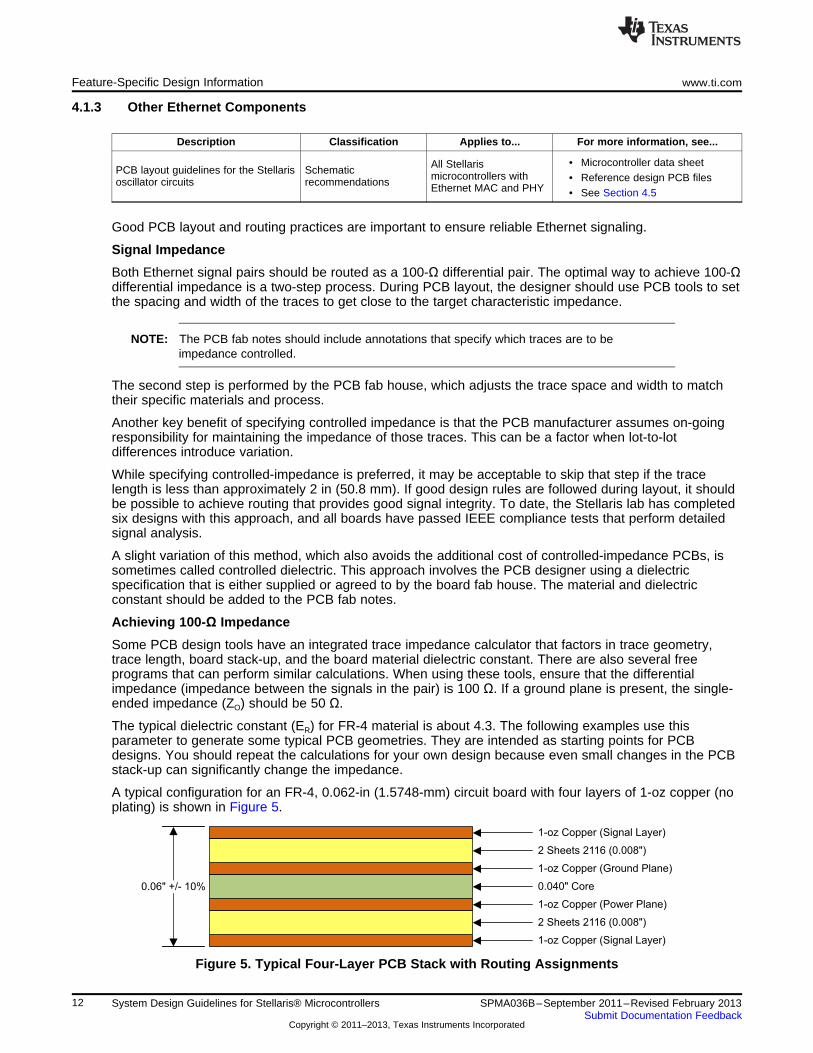
1-oz Copper (Signal Layer)
1-oz Copper (Power Plane)
1-oz Copper (Ground Plane)
1-oz Copper (Signal Layer)
2 Sheets 2116 (0.008")
2 Sheets 2116 (0.008")
0.040" Core0.06" +/- 10%
Feature-Specific Design Information www.ti.com
4.1.3 Other Ethernet Components
Description Classification Applies to... For more information, see...
• Microcontroller data sheetAll StellarisPCB layout guidelines for the Stellaris Schematic microcontrollers with • Reference design PCB filesoscillator circuits recommendations Ethernet MAC and PHY • See Section 4.5
Good PCB layout and routing practices are important to ensure reliable Ethernet signaling.
Signal Impedance
Both Ethernet signal pairs should be routed as a 100-Ω differential pair. The optimal way to achieve 100-Ωdifferential impedance is a two-step process. During PCB layout, the designer should use PCB tools to setthe spacing and width of the traces to get close to the target characteristic impedance.
NOTE: The PCB fab notes should include annotations that specify which traces are to beimpedance controlled.
The second step is performed by the PCB fab house, which adjusts the trace space and width to matchtheir specific materials and process.
Another key benefit of specifying controlled impedance is that the PCB manufacturer assumes on-goingresponsibility for maintaining the impedance of those traces. This can be a factor when lot-to-lotdifferences introduce variation.
While specifying controlled-impedance is preferred, it may be acceptable to skip that step if the tracelength is less than approximately 2 in (50.8 mm). If good design rules are followed during layout, it shouldbe possible to achieve routing that provides good signal integrity. To date, the Stellaris lab has completedsix designs with this approach, and all boards have passed IEEE compliance tests that perform detailedsignal analysis.
A slight variation of this method, which also avoids the additional cost of controlled-impedance PCBs, issometimes called controlled dielectric. This approach involves the PCB designer using a dielectricspecification that is either supplied or agreed to by the board fab house. The material and dielectricconstant should be added to the PCB fab notes.
Achieving 100-Ω Impedance
Some PCB design tools have an integrated trace impedance calculator that factors in trace geometry,trace length, board stack-up, and the board material dielectric constant. There are also several freeprograms that can perform similar calculations. When using these tools, ensure that the differentialimpedance (impedance between the signals in the pair) is 100 Ω. If a ground plane is present, the single-ended impedance (ZO) should be 50 Ω.
The typical dielectric constant (ER) for FR-4 material is about 4.3. The following examples use thisparameter to generate some typical PCB geometries. They are intended as starting points for PCBdesigns. You should repeat the calculations for your own design because even small changes in the PCBstack-up can significantly change the impedance.
A typical configuration for an FR-4, 0.062-in (1.5748-mm) circuit board with four layers of 1-oz copper (noplating) is shown in Figure 5.
Figure 5. Typical Four-Layer PCB Stack with Routing Assignments
12 System Design Guidelines for Stellaris® Microcontrollers SPMA036B–September 2011–Revised February 2013Submit Documentation Feedback
Copyright © 2011–2013, Texas Instruments Incorporated

1-oz Copper (Signal Layer)
1-oz Copper (Power Plane)
1-oz Copper (Ground Plane)
1-oz Copper (Signal Layer)
2 Sheets 2116 (0.008")
2 Sheets 2116 (0.008")
0.040" Core
+ -
0.012" 0.024" 0.012"
+
Er
-
+ -
W S W
H
W S W
Microstrip Stripline
T
T
www.ti.com Feature-Specific Design Information
For this example, we place a solid ground plane on layer 2. The 1-oz copper plane is 1.4 mils (.0014 in, or0.0355 mm) thick. The height of traces above the ground plane is defined by the thickness of the PCBprepreg material—in this case, 0.008 in (0.2032 mm) thick. Therefore, total thickness is:
Total thickness = 0.062 in = 4 x 0.0014 in + 0.040 in + 2 x 0.008 in
Before calculating the trace width and spacing needed for 100-Ω impedance, we must determine the typeof transmission line model to use.
A PCB with a conductor bounded by a single ground reference plane is known as a microstrip, as shownin Figure 6.
Figure 6. Transmission Lines for Ethernet Signaling
Microstrip transmission lines are most common on boards with two to six layers and are entirely suitablefor Ethernet signaling. A more advanced configuration, known as stripline, uses two ground-referenceplanes which are typically stitched together with vias to form a coaxial cable-like transmission path.
Using the free PCB ToolKit calculator from Saturn PCB Design, Inc., results in the following values for theboard stack shown in Figure 7.
Conductor width (W) = 0.012 in (0.3048 mm)Conductor spacing (S) = 0.024 in (0.6096 mm)Substrate thickness (H) = 0.008 in (0.2032 mm)ZDifferential = 100.1 ΩZO = 54 Ω
HyperLynx from Mentor graphics gives the following similar results:Conductor width (W) = 0.012 in (0.3048 mm)Conductor spacing (S) = 0.024 in (0.6096 mm)Substrate thickness (H) = 0.008 in (0.2032 mm)ZDifferential = 100.1 ΩZO = 54.2 Ω
The HyperLynx model is more complete because it also factors in the ER of the soldermask as shown inFigure 7.
Figure 7. 100-Ω Microstrip Differential Pair on a Four-Layer, 0.06-in FR-4 PCB Stack
13SPMA036B–September 2011–Revised February 2013 System Design Guidelines for Stellaris® MicrocontrollersSubmit Documentation Feedback
Copyright © 2011–2013, Texas Instruments Incorporated

Feature-Specific Design Information www.ti.com
For a two-layer board, the height of the substrate is now the full thickness of the FR-4 PCB material. Thismakes it difficult to achieve anything close to 50-Ω single-ended impedance (ZO). However, because theZO parameter is less critical, we can still solve dimensions for the differential impedance. The followinganalysis was performed with HyperLynx because the dimensional aspect ratio is not supported by the freeSaturn PCB Design tool.
Conductor width (W) = 0.018 in (0.4572 mm)Conductor spacing (S) = 0.007 in (0.1778 mm)ZDifferential = 100.5 ΩZO = 100.7 Ω
Other Design Rules and Considerations
Follow these additional design rules and recommendations for best results:
• Apply the rules for high-speed signal routing listed elsewhere in this application report.
• Maintain symmetry when routing differential pairs. Some PCB layout tools can assist with this type ofrouting.
• Avoid vias if possible. If it is necessary to switch layers, then both signals in the pair should passthrough a via at the same distance on the trace.
• Avoid stubs.
• Route differential signal pairs on the same layer.
• Separate Ethernet signal pairs from each other by at least 0.050 in (1.27 mm). This requirement isnecessary to avoid cross-coupling between the RX and TX pairs.
• Place Ethernet resistors as close as possible to the Stellaris microcontroller.
• Do not extend a ground plane under the transformer, if using an unshielded transformer.
• Place 10-pF capacitors close to the Ethernet transformer.
Ethernet and Power Planes
A continuous ground plane is a good PCB design practice; however, there are special considerationswhen using planes and copper pours near Ethernet signals. The following restrictions apply only toEthernet circuits; general information on the recommended attributes of power planes are coveredelsewhere in this application report.
Strict requirements for planes near Ethernet circuits:
• Do not extend the power plane (that is, the VDD plane) under the Ethernet signals unless there is asolid ground plane between the differential Ethernet signals and the power plane.
• Make sure there are no ground plane discontinuities under or near the differential signals. This ruleapplies to all signals routed over planes.
• Do not extend the ground plane under the transformer unless it is shielded on all sides.
• Do not extend the ground plane under the signals from the transformer to the connector.
Other ground plane considerations:
• A ground plane is not strictly a requirement for Ethernet signalling. Retaining the ground planebetween the microcontroller and the transformer has several benefits, including:
– It provides a low-impedance connection point for the 10-pF filter capacitors. If correctly installed,these capacitors can improve Ethernet electromagnetic compatibility (EMC).
– Impedances are easier to control with a ground-reference plane. Without the plane, smalldimensional variations in the PCB have a more significant impact on the differential impedance.
– Smaller trace geometries are possible. Without a plane, simulations show that 0.023-in (0.5842-mm) traces with 0.007-in (0.1778-mm) spacing are needed for a typical two-layer FR-4 design.
• It may be difficult to implement a trace geometry that achieves both 100-Ω differential impedance and50-Ω single-ended impedance. The most critical parameter to optimize in this design is differentialimpedance.
14 System Design Guidelines for Stellaris® Microcontrollers SPMA036B–September 2011–Revised February 2013Submit Documentation Feedback
Copyright © 2011–2013, Texas Instruments Incorporated

www.ti.com Feature-Specific Design Information
4.2 Ethernet and USB
This section describes design considerations related to the microcontroller Ethernet and USB modules.
4.2.1 Bias Resistors
Description Classification Applies to... For more information, see...
Selection and routing information on the Schematic and layout All Stellaris microcontrollers • Microcontroller data sheetbias resistor recommendations with Ethernet or USB • Evaluation board schematics
All Stellaris microcontrollers with integrated Ethernet or USB may require 1% precision bias resistors toprovide an accurate reference for the PHY circuitry. The Ethernet PHY requires a 12.4-kΩ resistor and theUSB controller may require a 9.10-kΩ resistor.
Bias resistors must be located close to the microcontroller pin (ideally less than 0.25 in, or 6 mm). Theother resistor terminal should have a very short trace directly to GND. The trace/via for the GNDconnection should not be shared with any other pin.
4.2.2 Other PCB Design Rules
Description Classification Applies to... For more information, see...
Schematic All Stellaris microcontrollers • Microcontroller data sheetGeneral guidelines for PCB design recommendations with Ethernet or USB • Evaluation board schematics
While solid ground and power planes are highly desirable, small areas of copper pour should be usedcautiously. It is often not a good idea to pour every available area on the routing layers of multi-layerboards. On one- and two-layer board designs, multiple pours might be necessary, because dedicatedplane layers are not available.
If used, never leave small copper pours floating or unconnected. Isolated conductor areas can causeunwanted coupling and EMC problems if they act as an antenna. Small copper pours should have solidconnections to a ground net/trace. Ideally, use several vias to provide a low-impedance connection.
4.2.3 Chassis Ground
Description Classification Applies to... For more information, see...
How and when to use a chassis ground to Schematic and PCB layout All Stellaris microcontrollers Evaluation board schematicsachieve optimal EMC recommendations with Ethernet or USB
When properly designed, a chassis ground routed on the PCB can be a very effective feature foraddressing a range of EMC challenges.
One specific benefit is improved electro-static discharge (ESD) immunity due to the provision of a safedischarge path that avoids sensitive circuitry in the center of the board.
In general, a chassis ground on the PCB works in conjunction with the overall enclosure to improveelectro-magnetic emissions and especially immunity.
The chassis ground should be routed or poured copper around the perimeter of the PCB, ideally on alllayers. If the ground is not present on all PCB layers, then other layers should be pulled back from thechassis ground to avoid coupling. The chassis ground should not route over the top of any power orground layer.
Typically, the chassis ground should have a break or void in to prevent loops that could cause loopantenna effects. However, depending on the size of the board, enclosure design, and ground connectionpoint locations, it might still be acceptable or preferable to have a continuous chassis ground around theboard.
A chassis ground is particularly important in systems with external connectors, metal enclosures, orapertures in the enclosure (see Figure 8).
15SPMA036B–September 2011–Revised February 2013 System Design Guidelines for Stellaris® MicrocontrollersSubmit Documentation Feedback
Copyright © 2011–2013, Texas Instruments Incorporated

Chassis Ground Plane
RJ45
Signal Ground Plane
USB
Stellaris®
MCUGap to avoid
loop antenna
Capacitor for ESD discharge path
(sometimes included in Ethernet magnetics)
No plane under
Ethernet transformer
Feature-Specific Design Information www.ti.com
Figure 8. Chassis Ground Guidelines
4.3 USB
Description Classification Applies to... For more information, see...
• Microcontroller data sheetAll StellarisPCB layout guidelines for the Stellaris PCB layout microcontrollers with a • Evaluation board schematicsUSB signals recommendations USB module • See Section 4.5
Good PCB layout and routing practices are important in ensuring reliable USB signalling. Routing the D+and D– differential pair is the most important consideration. VBUS and ID (typically used only in USB OTGand dual-mode applications) signal routing is not critical as these are low-speed signals.
4.3.1 Signal Impedance
The USB D+ and D- signal pair should be routed as a 100-Ω differential pair.
The optimal way to achieve 90-Ω differential impedance is a two-step process. During PCB layout, thedesigner should use PCB tools to set the spacing and width of the traces to get close to the targetcharacteristic impedance.
NOTE: The PCB fab notes should include annotation that specifies which traces are to beimpedance controlled.
The second step is performed by the PCB fab house, which adjusts the trace space and width to matchtheir specific materials and process.
Another key benefit of specifying controlled impedance is that the PCB manufacturer assumes on-goingresponsibility for maintaining the impedance of those traces. This can be a factor when lot-to-lotdifferences introduce variation.
While specifying controlled-impedance is preferred, it may be acceptable to skip that step if the tracelength is less than approximately 2 in (5.08 cm). If good design rules are followed during layout, it shouldbe possible to achieve routing that provides good signal integrity. To date, the Stellaris lab has completedsix designs with this approach and all boards have passed IEEE compliance tests that perform detailedsignal analysis.
16 System Design Guidelines for Stellaris® Microcontrollers SPMA036B–September 2011–Revised February 2013Submit Documentation Feedback
Copyright © 2011–2013, Texas Instruments Incorporated

1-oz Copper (Signal Layer)
1-oz Copper (Power Plane)
1-oz Copper (Ground Plane)
1-oz Copper (Signal Layer)
2 Sheets 2116 (0.008")
2 Sheets 2116 (0.008")
0.040" Core
90 Microstrip Differential Pair onΩ
a 4-layer 0.06" FR-4 PCB stack
+ -
0.010" 0.008" 0.010"
1-oz Copper
1-oz Copper
1-oz Copper
1-oz Copper
2 Sheets 2116 (0.008")
2 Sheets 2116 (0.008")
0.040" Core0.06" +/- 10%
Typical 4 Layer PCB Stack
www.ti.com Feature-Specific Design Information
A slight variation of this method, that also avoids the additional cost of controlled-impedance PCBs, issometimes called controlled dielectric. This approach involves the PCB designer using a dielectricspecification that is either supplied or agreed to by the board fab house. The material and dielectricconstant should be added to the PCB fab notes.
4.3.2 Achieving 90-Ω Impedance
Some PCB design tools have an integrated trace impedance calculator that factors in trace geometry,trace length, board stack-up, and the board material dielectric constant. There are also several freeprograms that can perform similar calculations. When using these tools, ensure that the differentialimpedance (impedance between the signals in the pair) is 90 Ω. If a ground plane is present, the single-ended impedance (ZO) should be 50 Ω.
The typical dielectric constant (ER) for FR-4 material is approximately 4.6.
A typical configuration for an FR-4, 0.062-in (1.574-mm) circuit board with four layers of 1-oz copper and1/2-oz plating is shown in Figure 9.
Figure 9. Typical Four-Layer PCB Stack
For this example, we place a solid ground plane on layer 2. The 1-oz copper plane is 1.4 mils (0.0014 in,or 0.0355 mm) thick. The height of traces above the ground plane is defined by the thickness of the PCBprepreg material—in this case 0.008 in (0.2032 mm) thick. Therefore, total thickness is:
Total thickness = 0.062 in = 4 x 0.0014 in + 0.040 in + 2 x 0.008 in
Using the free PCB ToolKit calculator from Saturn PCB Design, Inc., results in the following values for theboard stack shown in Figure 10.
Conductor width (W) = 0.010 in (0.254 mm)Conductor spacing (S) = 0.008 in (0.2032 mm)ZDifferential = 90 ΩZO = 55 Ω
Figure 10. 90-Ω Microstrip Differential Pair on a Four-Layer, 0.06-in FR-4 PCB Stack
17SPMA036B–September 2011–Revised February 2013 System Design Guidelines for Stellaris® MicrocontrollersSubmit Documentation Feedback
Copyright © 2011–2013, Texas Instruments Incorporated

Feature-Specific Design Information www.ti.com
The PCB fabricator improves the value and tolerance of these results if the traces are specified ascontrolled-impedance.
For a two-layer board, the height of the substrate is now the full thickness of the FR-4 PCB material. Theheight of the substrate means that much wider traces are needed to achieve 90-Ω impedance. Thefollowing analysis was performed with HyperLynx because the dimensional aspect ratio is not supportedby the free Saturn PCB Design tool.
Conductor width (W) = 0.028 in (0.7112 mm)Conductor spacing (S) = 0.007 in (0.1778 mm)ZDifferential = 90 ΩZO = 91.5 Ω
4.3.3 Other Design Rules and Considerations
Follow these additional design rules and recommendations for best results:
• Apply the rules for high-speed signal routing listed elsewhere in this application report.
• Maintain symmetry when routing differential pairs. Some PCB layout tools can assist with this kind ofrouting. Avoid vias if possible. If it is necessary to switch layers, then both signals in the pair shouldpass through a via at the same distance on the trace.
• Avoid stubs when adding components to D+ and D– signals. Devices such as ESD suppressors shouldbe located directly on the signal trace.
• Route differential signal pairs on the same layer.
4.4 EPI
Description Classification Applies to... For more information, see...
Routing recommendations for high- Schematic All Stellaris • Microcontroller data sheetspeed signals used by the External recommendations microcontrollers with EPI • Evaluation board schematicsPeripheral Interface (EPI) module
The External Peripheral Interface (EPI) module is a high-bandwidth bus that can interface to various kindsof external memory and other devices. Due to the speed and special timing requirements of this interface,special layout considerations are necessary.
In EPI mode, Stellaris microcontroller pins are characterized with a 16-pF load rather than a 50-pF load.To maintain timing margins over the full operating speed of the EPI module, EPI signal capacitance mustbe 16 pF or less and the GPIO drive-strength should be set to 8 mA. This includes both the load and tracecapacitance. It is not necessary to include the Stellaris microcontroller pin and pad characteristic whenevaluating total capacitive loading.
For SDRAM and multiplexed host-bus modes, it is important to factor in multiple loads on some EPIsignals. For example, in SDRAM mode, EPIxS0...EPIxS14 are used to drive both address and datasignals to the SDRAM. For a Micron MT48LC4M16A2 SDRAM in a TSOP package, for example, theaddress inputs have a worst-case capacitance of 3.8 pF and the data lines (DQs) of 6.0 pF. Deductingthese values from 16 pF results in an allowance of about 8 pF for trace capacitance.
Using the 0.062-in, four-layer FR4 PCB stack-up from the DK-LM3S9x96 Development Kit, we cancalculate the capacitance per inch for an 0.008-in (0.2032-mm) trace. The HyperLynx and Saturn PCB toolkits both provide capacitance values of approximately 1.8 pF/inch. So the maximum trace length is 6.2 pF/ (1.8 pF/inch) = 3.44 in (8.737 cm)
The Stellaris DK-LM3S9B96 Development board has worst-case trace length on the SDCLK signal of 3.15in (8.001 cm) on the main board and 0.225 in (5.715 mm) on the SDRAM board. This total length is lessthan the 3.44 in (8.737 cm) target. The EPI signals do pass through a board-to-board connector but thecapacitance to ground is very small and can be ignored. Design tools should be used to calculate themaximum allowable trace length for a specific design based on PCB geometry and materials.
18 System Design Guidelines for Stellaris® Microcontrollers SPMA036B–September 2011–Revised February 2013Submit Documentation Feedback
Copyright © 2011–2013, Texas Instruments Incorporated

50
Ω
Poor differential pair routing
50Ω
Very poor stub length
Resistors should be
located at the same
distance on the
trace pair
Improved differential pair routing
50
Ω50
Ω
0Ω
Plane A
Plane B
Do not route signals over
non-continuous plane
0Ω
Plane A
Plane B
Good PCB trace routingPoor PCB trace routing
www.ti.com Feature-Specific Design Information
4.5 General Guidelines for All High-Speed Interfaces
This section describes design considerations related to the microcontroller Ethernet, USB, EPI, and otherhigh-speed interfaces.
4.5.1 PCB Design Rules: Other Routing Guidelines
Description Classification Applies to... For more information, see...
All Stellarismicrocontrollers withGeneral rules for routing PCB traces PCB layout • Microcontroller data sheetEthernet, USB, EPI, oron high-speed nets recommendations • Reference design PCB filesother high-speedinterface
Avoid discontinuities in ground planes and power planes under high-speed signals as shown in Figure 11.For controlled-impedance interfaces such as Ethernet and USB, discontinuities create impedance changesthat impact signal integrity. For all signals, a break in the ground plane removes a direct path for anyreturn current to flow through. This consideration is important even for balanced differential pairs becauseperfect matching is seldom achievable and ground current is inevitable.
Figure 11. Examples of PCB Trace Layout
Avoid stubs in differential signal pairs where possible (see Figure 12). Where termination or bias resistorsare needed, one terminal should be located directly on the trace. Both resistors should be located at thesame distance from the source and load.
Figure 12. Examples of Differential Pair Layout
19SPMA036B–September 2011–Revised February 2013 System Design Guidelines for Stellaris® MicrocontrollersSubmit Documentation Feedback
Copyright © 2011–2013, Texas Instruments Incorporated

Feature-Specific Design Information www.ti.com
Stellaris microcontrollers provide programmable drive strength for all digital output pins. To improve theperformance of digital signals, set the GPIO drive strength register appropriately. Selecting a lower drivestrength can avoid signal integrity issues due to ringing and reflections. If the drive strength is too low,however, timing and rise and fall time requirements may not be satisfied.
4.6 ADC
This section describes design considerations related to the microcontroller ADC module.
4.6.1 ADC Input Schematics
Description Classification Applies to... For more information, see...
How to achieve optimal ADC All StellarisSchematic • Microcontroller data sheetperformance through careful circuit microcontrollers withrecommendations • Reference design schematicsdesign ADC
In order to achieve the best possible conversion results from an ADC, it is important to start with a goodschematic design.
All ADCs require a voltage reference (or occasionally a current reference), whether the voltage referenceis provided from an on-chip source or via an external pin. Any deviation in the reference voltage from itsideal level results in additional gain error (or slope error) in the conversion result.
Stellaris LM3S microcontrollers incorporate an internal voltage reference that can save the cost of anexternal reference device. Stellaris LM4F microcontrollers offer greater ADC precision and require anexternal reference voltage. The LM4F circuit should provide a precision voltage source to either the VREF+
or VDDA pin. The designer should determine whether the internal reference has sufficient accuracy or if anexternal reference is needed. If an external reference is used, it should be used with capacitors on boththe supply pin and the output pin. See the voltage reference in the corresponding microcontroller datasheet for recommendations on value. Typically, 1 μF or more is recommended.
Optimal ADC accuracy is achieved with a low-impedance source and a large input filter capacitor. As thesignal source impedance increases and capacitance decreases, noise on the conversion result increases.Noise sources include coupling from other signals, power supplies, external devices, and from themicrocontroller itself. Refer to the respective microcontroller data sheet for source impedancerecommendations for LM4F devices.
If resistor dividers are used to scale an input voltage, then best results can be achieved with low-valueresistors. The resistor from the ADC input to ground should ideally be less than 1 kΩ. Avoid values higherthan 10 kΩ unless a large filter capacitor is present.
Ceramic filter capacitors of 1 μF or more can substantially improve noise performance. The trade-off is areduction in signal bandwidth (as a function of the source impedance) and phase shifting.
Input protection should also be considered, especially when converting signals from external devices orwhere transient voltages might be present. The ADC pins on some Stellaris devices (in ADC mode) arenot 5-V tolerant, but do allow some margin over the +3.0-V span. See the respective microcontroller datasheet for specific information.
Increased source impedance can provide a degree of protection to the ADC. Semiconductor clampingcircuits can also be used—typically, zener diodes or clamping diodes to 3 V and GND. When specifyingdiodes, consider leakage current over temperature (IR) because this parameter affects overall conversionaccuracy.
20 System Design Guidelines for Stellaris® Microcontrollers SPMA036B–September 2011–Revised February 2013Submit Documentation Feedback
Copyright © 2011–2013, Texas Instruments Incorporated

www.ti.com PCB Layout Examples
5 PCB Layout Examples
This section provides PCB layout examples for a 100-pin TQFP package and a 48-pin TQFP package.
5.1 TQFP 100-Pin Routing
Description Classification Applies to... For more information, see...
An example of a two-layer PCB layout for a • Microcontroller data sheetStellaris LM3S9B90 microcontroller in a 100-pin PCB layout recommendations All Stellaris microcontrollersTQFP package • Evaluation board schematics
Figure 13. Stellaris LM3S9B90 Microcontroller Minimal Circuit
Figure 13 shows a minimal circuit for an LM3S9B90 Stellaris microcontroller with Ethernet, USB, andHibernate modules. Pull-up resistors might also be needed on JTAG signals if these pins are not drivenexternally. VDD, VDDC, and GND connections are shown as thick PCB traces for clarity. Normally theseconnections would be extended as copper pours.
• R1 Reset input pull-up resistor
• C1 Reset input filter capacitor
• C3 LDO regulator filter capacitor
• C2, C4-C6, C11 VDD Decoupling capacitors
• C7, C18 VDDC Decoupling capacitors
• C12-C17 Crystal load capacitors
• Y1 Ethernet Crystal
• Y2 Main Oscillator Crystal
• Y3 Hibernate Module Crystal
• R3 Ethernet RBIAS resistor
• R2 Hibernate Oscillator resistor
• R5 USB RBIAS
• R4 MDIO Pull-up resistor
21SPMA036B–September 2011–Revised February 2013 System Design Guidelines for Stellaris® MicrocontrollersSubmit Documentation Feedback
Copyright © 2011–2013, Texas Instruments Incorporated

PCB Layout Examples www.ti.com
5.2 TQFP 48-Pin Routing
Description Classification Applies to... For more information, see...
An example of a two-layer PCB layoutfor a Stellaris LM3S811 PCB layout All Stellaris • Microcontroller data sheetmicrocontroller in a 48-pin TQFP recommendations microcontrollers • Evaluation board schematicspackage
Figure 14 shows a minimal circuit for an LM3S811 Stellaris microcontroller. Pull-up resistors might beneeded on PB7/TRST and JTAG signals if these pins are not driven externally.
Figure 14. Stellaris LM3S811 Microcontroller Minimal Circuit
22 System Design Guidelines for Stellaris® Microcontrollers SPMA036B–September 2011–Revised February 2013Submit Documentation Feedback
Copyright © 2011–2013, Texas Instruments Incorporated

www.ti.com System Design Examples
6 System Design Examples
For example designs using Stellaris microcontrollers, see Table 2 for the detailed list of StellarisReference Design Kits (RDKs), Evaluation Kits (EKs), and Development Kits (DKs).
Schematics are available for all designs. Full PCB design files including Gerber files are available forStellaris reference designs only.
Table 2. Stellaris Example Designs
PCBDevicePart Number Description Stellaris Devices Key Features LayerPackage Count
EK-LM3S811 Evaluation Board LM3S811 LQFP48 ADC, motion control 4
EK-LM3S1968 Evaluation Board LM3S1968 LQFP100 ADC, motion control 4
EK-LM32965 CAN Evaluation Board LM3S2965 LQFP100 CAN 4
EK-LM3S3748 USB Evaluation Board LM3S3748 LQFP100 USB 4
EK-LM3S6965 Ethernet Evaluation Board LM3S6965 LQFP100 Ethernet 4
CAN and Ethernet EvaluationEK-LM3S8962 LM3S8962 LQFP100 CAN, Ethernet 4Board
EK-LM3S9x90 Evaluation Board LM3S9x90 LQFP100 USB, Ethernet 4
EK-LM3S9x92 Evaluation Board LM3S9x92 LQFP100 USB, Ethernet 4
USB, hibernate, real-timeEK-LM4F232 Evaluation Board LM4F232H5QD LQFP144 6clock
EK-LM4F120XL LaunchPad Evaluation Board LM4F120H5QR LQFP64 Simple two-layer layout 2
DK-LM3S9D96 Development Kit LM3S9D96 LQFP100 USB, CAN, Ethernet, EPI 4
7 Conclusion
Applying good system-design practices from the earliest design stages ensures a successful board bring-up. The design process should include thorough design-reviews using the information in this applicationreport, other embedded system design resources, and reports created by the design team. These effortswill be rewarded with a reliable and properly performing Stellaris microcontroller-based design.
The use of the StellarisWare® Peripheral Driver Library also minimizes software changes to the start-uproutines that configure the I/O, enabling application code to be moved to the new devices with minimalfunctional changes.
8 References
The following related documents and software are available on the Stellaris web site atwww.ti.com/stellaris:
• Stellaris LM3S Microcontroller Data Sheet (individual device documents available through productselection tool).
• StellarisWare Driver Library. Available for download at www.ti.com/tool/sw-drl.
• StellarisWare Driver Library User’s Manual, publication SW-DRL-UG (literature number SPMU019).
23SPMA036B–September 2011–Revised February 2013 System Design Guidelines for Stellaris® MicrocontrollersSubmit Documentation Feedback
Copyright © 2011–2013, Texas Instruments Incorporated

IMPORTANT NOTICE
Texas Instruments Incorporated and its subsidiaries (TI) reserve the right to make corrections, enhancements, improvements and otherchanges to its semiconductor products and services per JESD46, latest issue, and to discontinue any product or service per JESD48, latestissue. Buyers should obtain the latest relevant information before placing orders and should verify that such information is current andcomplete. All semiconductor products (also referred to herein as “components”) are sold subject to TI’s terms and conditions of salesupplied at the time of order acknowledgment.
TI warrants performance of its components to the specifications applicable at the time of sale, in accordance with the warranty in TI’s termsand conditions of sale of semiconductor products. Testing and other quality control techniques are used to the extent TI deems necessaryto support this warranty. Except where mandated by applicable law, testing of all parameters of each component is not necessarilyperformed.
TI assumes no liability for applications assistance or the design of Buyers’ products. Buyers are responsible for their products andapplications using TI components. To minimize the risks associated with Buyers’ products and applications, Buyers should provideadequate design and operating safeguards.
TI does not warrant or represent that any license, either express or implied, is granted under any patent right, copyright, mask work right, orother intellectual property right relating to any combination, machine, or process in which TI components or services are used. Informationpublished by TI regarding third-party products or services does not constitute a license to use such products or services or a warranty orendorsement thereof. Use of such information may require a license from a third party under the patents or other intellectual property of thethird party, or a license from TI under the patents or other intellectual property of TI.
Reproduction of significant portions of TI information in TI data books or data sheets is permissible only if reproduction is without alterationand is accompanied by all associated warranties, conditions, limitations, and notices. TI is not responsible or liable for such altereddocumentation. Information of third parties may be subject to additional restrictions.
Resale of TI components or services with statements different from or beyond the parameters stated by TI for that component or servicevoids all express and any implied warranties for the associated TI component or service and is an unfair and deceptive business practice.TI is not responsible or liable for any such statements.
Buyer acknowledges and agrees that it is solely responsible for compliance with all legal, regulatory and safety-related requirementsconcerning its products, and any use of TI components in its applications, notwithstanding any applications-related information or supportthat may be provided by TI. Buyer represents and agrees that it has all the necessary expertise to create and implement safeguards whichanticipate dangerous consequences of failures, monitor failures and their consequences, lessen the likelihood of failures that might causeharm and take appropriate remedial actions. Buyer will fully indemnify TI and its representatives against any damages arising out of the useof any TI components in safety-critical applications.
In some cases, TI components may be promoted specifically to facilitate safety-related applications. With such components, TI’s goal is tohelp enable customers to design and create their own end-product solutions that meet applicable functional safety standards andrequirements. Nonetheless, such components are subject to these terms.
No TI components are authorized for use in FDA Class III (or similar life-critical medical equipment) unless authorized officers of the partieshave executed a special agreement specifically governing such use.
Only those TI components which TI has specifically designated as military grade or “enhanced plastic” are designed and intended for use inmilitary/aerospace applications or environments. Buyer acknowledges and agrees that any military or aerospace use of TI componentswhich have not been so designated is solely at the Buyer's risk, and that Buyer is solely responsible for compliance with all legal andregulatory requirements in connection with such use.
TI has specifically designated certain components as meeting ISO/TS16949 requirements, mainly for automotive use. In any case of use ofnon-designated products, TI will not be responsible for any failure to meet ISO/TS16949.
Products Applications
Audio www.ti.com/audio Automotive and Transportation www.ti.com/automotive
Amplifiers amplifier.ti.com Communications and Telecom www.ti.com/communications
Data Converters dataconverter.ti.com Computers and Peripherals www.ti.com/computers
DLP® Products www.dlp.com Consumer Electronics www.ti.com/consumer-apps
DSP dsp.ti.com Energy and Lighting www.ti.com/energy
Clocks and Timers www.ti.com/clocks Industrial www.ti.com/industrial
Interface interface.ti.com Medical www.ti.com/medical
Logic logic.ti.com Security www.ti.com/security
Power Mgmt power.ti.com Space, Avionics and Defense www.ti.com/space-avionics-defense
Microcontrollers microcontroller.ti.com Video and Imaging www.ti.com/video
RFID www.ti-rfid.com
OMAP Applications Processors www.ti.com/omap TI E2E Community e2e.ti.com
Wireless Connectivity www.ti.com/wirelessconnectivity
Mailing Address: Texas Instruments, Post Office Box 655303, Dallas, Texas 75265Copyright © 2013, Texas Instruments Incorporated
Recommended