Synthesis and electrical properties of fullerene-based
molecular junctions on silicon substrate
D. Guérin, S. Lenfant, S. Godey, D. Vuillaume
Molecular Nanostuctures and Devices group, Institut d'Electronique, Micro-électronique et
Nanotechnologie , CNRS, University of Lille, BP60069, avenue Poincaré, F-59652 cedex,
Villeneuve d'Ascq (France)
We report the synthesis and the electrical properties of fullerene-based molecular junctions on
silicon substrate in which the highly π-conjugated molecule C60 (π quantum well) is isolated
from the electrodes by alkyl chains (σ tunnel barriers). Initially, the Si/SiO2/σC60 architecture
was prepared either by sequential synthesis (3 different routes) or by direct grafting of the
presynthesized C60-σ-Si(OEt)3 molecule. We described the chemical synthesis of these routes
and the physico-chemical properties of the molecular monolayers. Then, the second σ tunnel
barrier was added on the Si/SiO2/σC60 junction by applying a hanging mercury drop electrode
thiolated with an alkanethiol monolayer. We compared the electronic transport properties of
the Si/SiO2/σC60//Hg and Si/SiO2/σC60//σHg molecular junctions, and we demonstrated by
transition voltage spectroscopy that the fullerene LUMO - metal Fermi energy offset can be
tailored from ~ 0.2 eV to ~ 1 eV by changing the length of the alkyl chain between the C60
core and the Hg metal electrode (i. e. from direct C60//Hg contact to 14 carbon atoms tunnel
barrier).
Surface functionalization utilizing buckminsterfullerene C60 is of great interest, owing to the
possibility of transferring the exceptional electronic (superconductivity, switching, memory),
optoelectronic and magnetic properties1 of this molecule on the surface of bulk materials. The
electronic structure of this highly π-conjugated molecule with relatively high electron affinity
(2.65 eV)2 and low band gap (1.6 eV)
3 makes it a strong electron-accepting group coveted in
numerous applications, particularly in nanoelectronics. For instance, high electron field effect
mobility (0.2 cm2/Vs) in n-channel Organic Thin Film Transistors (OTFT) has been reported
for C60 film on HMDS modified SiO2 as gate dielectic.4 Resonant tunneling effect has been
observed by Grüter et al.5 in a thiolated C60 molecular junction prepared by break junction
method between gold electrodes. Bistable and negative differential resistance (NDR) effects
have been observed in single layer devices made from fullerenes mixed with polystyrene and
sandwiched between two Al electrodes.6 It has been recently reported several C60-based
unimolecular rectifiers with high rectification ratios up to 158 at 3 V.7
To our knowledge, all the previously reported studies in the field of nanoelectronics on C60-
based molecular junctions concerned C60 deposited by vacuum evaporation8, by the
Langmuir-Blodgett technique9, C60 inserted in mechanically break junction
5, e-beam
lithographed nano-gap10
, or scanning tunneling microscopy (STM)11
test-beds. Here we report
on molecular junctions on silicon based on self-assembled monolayers (SAMs) including C60
molecules.
Electronic coupling between molecules and electrodes is a key point impacting the electron
transport in molecular junctions. For instance, many groups have reported on the influence of
the chemical nature of the chemical linker (e.g. thiol, selenol, amine, phosphine…) between
the molecule and a metal electrode.12
In SAM rectifying diodes based on the silicon/σ-π/metal
architecture, Fermi-level pinning at the π group/metal interface has been identified as the

main responsible for the absence of dependence of the rectification effect as a function of the
chemical nature of the π groups, although these groups have significant differences in their
electronic structure (i.e. different HOMO and LUMO energy levels).13
This effect has been
interpreted as resulting from orbital overlaps between metal and π groups which create new
chemically-induced gap states at the metal/organic interface.
Here, we report results on the dependence of this orbital coupling effect as function of the
length of the saturated spacer (σ chain) between the C60 core and the metal electrode. To this
end, we compared the electrical properties of two molecular architectures: Si/SiO2/σC60//Hg
and Si/SiO2/σC60//σHg junctions. In the first architecture, π-conjugated group was directly in
contact with the metal whereas in the second one, C60 core was isolated between two alkyl
chains (called σ tunnel barriers). Natively oxidized silicon (~10 Å) was used. Metal electrode
was deposited on the Si/SiO2/σC60 molecular junctions by applying hanging mercury drop on
the monolayer. Moreover, by treating the Hg drop electrode with alkylthiols SAMs of
different lengths, the π goup was isolated from the metal by a second σ tunnel barrier.
Electrical characterizations of the resulting Si/SiO2/σC60//Hg and Si/SiO2/σC60//σHg
molecular devices were compared.
Many strategies have been developed in the literature to realize the self-assembly of fullerene
and its derivatives on various surfaces.14
Among them are two commonly used methods : (a)
the sequential modification of the surface by adsorption of an organic monolayer bearing a
terminal reactive functionality such as amine15
, azide16
, or azomethine ylide17
group that
forms coupling reaction with C60, or (b) the direct assembly of prefunctionalized C60
derivatives bearing suitable group that binds the surface. Trialkoxysilane groups -Si(OR)3 are
appropriate functions in the case of oxidized silicon surface since they strongly chemisorb
forming dense and well-organized self assembled monolayers (SAMs).18
In the present work, we compared these two strategies (sequential and direct grafting) in order
to prepare good quality C60 monolayers on oxidized silicon. Physicochemical
characterizations of SAMs by several analytical tools (contact angle measurement,
ellipsometry, FTIR spectroscopy, X photoelectron spectroscopy, cyclic voltammetry) enabled
to select the best molecular junctions for their electrical characterization.
1- Synthesis of Si/SiO2/σC60 molecular junction by sequential routes.
We chose 3 sequential methods (schema 1) involving reactions of buckyball with SAMs
bearing 3 different reactive end-groups. The first two selected sequential routes were based on
the well-known 1,3-dipolar cycloaddition reaction of azomethine ylides to fullerene (also
called Prato reaction).19
In the presence of C60 the ylide adds to buckyball yielding a
monolayer in which a pyrrolidine ring is fused to C60 (i.e. fulleropyrrolidine). Azomethine
ylides are generated in situ either (sequential route 1) by a decarboxylation route17a
from
aldehyde terminated SAM and N-methylglycine at 180°C or (sequential route 2) by thermal
ring-opening of carbomethoxyaziridine-terminated SAM.20
The last sequential route brought
into play azide function as a reactive group in the presence of C60 (sequential route 3) giving
rise to fulleroaziridine adduct by thermolysis (and probably also azafulleroid and
polyazafulleroid derivatives not represented on schema 1).21
Between C60 core and silicon substrate, we voluntarily chose small alkyl spacers of only 3
carbon atoms playing the role of a small tunnel barrier (noted σ on schema 1) in order to not
restrict current density through the molecular junction. Precursor SAMs bearing aldehyde,

carbomethoxyaziridine and azide functions were prepared by classical silanization reaction.
The details of these syntheses and their physicochemical characterizations are given in the
supplementary information section.
C60 grafting by sequential route 1.
Among the several successful C60 functionalization methodologies reported in the past years,
the Prato reaction is certainly the most widely used. Therefore, it seemed of interest to
undertake grafting of C60 on the CHO-terminated SAM by the Prato reaction. Unlike results
obtained by Cattaruzza et al.17
from CHO-terminated long aliphatic chains on Si-H surface,
Prato reaction was unsatisfactory with our CHO-terminated SAM in the presence of C60 and
N-methylglycine. Indeed, solution turned dark red during the grafting reaction and by
products were observed in the medium by thin layer chromatography. We did not try to
isolate these by-products that probably resulted from side reactions of N-methylglycine with
fullerene. Literature results show that yields of Prato reactions are generally low in
homogeneous phase (~20-30%). Even if the film thickness seemed correct (16 Å), the static
water contact angle (44°) was too low compared to expected value15b,17,22
ranging from 65° to
76° for common C60 monolayers (table 1).
C60 grafting by sequential route 2.
Another option to generate azomethine ylide is the thermal ring-opening of
carbomethoxyaziridine. Carbomethoxyaziridine functionalized with trialkoxysilane group had
been already employed by Bianco et al. to synthesize a fullerene derivative bearing -Si(OEt)3
group which was then used to functionalize HPLC silica gel.14
To our knowledge, this
reaction had never been realized by sequential surface chemistry on SiO2 surface. We thus
realized thermolysis of carbomethoxyaziridine-terminated SAM in the presence of C60. Let
us precise that such a reaction required heating the medium at least at 80°C for several hours
and under these conditions the least oxidant or water traces damaged the SAM. We observed
that presence of a water trap (freshly activated molecular sieves) in the medium dramatically
reduced this problem but the reproducibility of the reaction remained low.
Static water contact angle (71°) was in agreement with literature values15b,17,22
but thickness
measurements (ranging from 15.4 Å to 44 Å) varied from sample to sample (table1). For most
samples, C60 multilayers were obtained suggesting strong physisorption of fullerene
aggregates on the substrate that intensive cleaning by sonication in different solvents could
not remove. Fullerene aggregation is an often observed phenomenon in surface
functionalization by C60.23
We wanted to confirm the presence of the electroactive specie C60 by cyclic voltammetry.
Figure 1 shows typical voltammograms obtained on C60 monolayers and multilayers used as
working electrodes. Depending on the number of fullerene layers, a more or less well-defined
irreversible wave was observed in the cathodic region. Even if peak intensities were quite low
due to the presence of resistive SiO2 layer (9.7 Å), the reduction potential at approximately -1
V/SCE was close to that observed for other SAMs containing C60.17a,15b
As a reference, a
saturated solution of C60 in toluene/CH2Cl2 presented 3 reduction peaks at -1.01, -1.31 and -
1.74 V/SCE, respectively (Cf. sequential route 3, fig. 5). These results tend to confirm the
presence of fullerene on the oxidized silicon surface but it should be admitted that the C60
grafting reaction is quite difficult to control and to reproduce by this method.

C60 grafting by sequential route 3.
The last sequential method brought into play thermolysis of N3-terminated SAM in the
presence of C60. After this surface treatment, static water contact angle (table 1) slightly
varied from 68° to 70° (typical literature value for C60 film), while SAM thickness increased
from 8 Å to 14 Å in agreement with theoretical MOPAC24
value (14.6 Å). Infrared
spectroscopy in ATR mode (Attenuated Total Reflexion), also confirmed disappearance of the
characteristic absorption peak associated to -N3 group at 2101 cm-1
due to decomposition by
thermolysis. Antisymmetric and symmetric -CH2- stretches were observed at 2933 and 2869
cm-l, respectively for N3-terminated SAM, while they were observed at 2927 and 2860 cm
-1,
respectively for C60-terminated SAM (figure 2). In crystalline aliphatic chains, antisymmetric
and symmetric -CH2- vibrations occur at 2918 and 2851 cm-l, respectively. It has been
established that absorptions due to -CH2- stretching vibrations shift to higher frequency when
disorder increases (and thus the chain length decreases) in monolayers.25
Here values
observed for -CH2- stretches are usual for small alkyl chains.
Vibration peaks related to C60 (i.e. C=C double bonds) could not be assigned due to the
complexity of spectra in the 700-1600 cm-1
region (which is also the vibration region of Si-O
bonds of the native silicon oxide). In a typical spectrum from literature26
, C60 moiety vibration
bands are observed at 526 (the most intense band), 630, 1180 and 1430 cm-1
.
XPS measurements were also achieved to follow sequential route 3. Figures 3(a) and 3(b)
show N1s core level peak on N3- and C60-terminated SAMs respectively. As expected, the
signature of azide group was evidenced on N3- terminated SAM by 2 components at 401.2 eV
and 404.9 eV with a characteristic area ratio of 2:1 respectively. The additional shoulder peak
at lower binding energy (400.5 eV) was assigned to amine function resulting from azide
decomposition under X ray radiation.27
After C60 grafting, as shown on figure 3(b), the two
high binding energy peaks characteristic of azide completely disappeared and a new N1s
component was found in the classical energy range of tertiary aliphatic amines at 399.9 eV in
accordance with the formation of fulleroaziridine derivatives on the surface. The noticeable
asymmetric shape of this N1s core level peak was due to the presence of another subjacent
component at about 401.9 eV attributed to protonated amine27
or to polynitrogen adducts such
as triazolines28
since multiple addition and rearrangement reactions between C60 and azides
may occur.21
C60 grafting was evidenced by the clear increase of C/N atomic ratio by a factor
of about 5 between the N3- and C60- terminated SAMs (see figure 4). Nevertheless, the
expected theoretical increase of C/N is 18, as C/N values should be 1 for the N3- terminated
SAM, and 18 for the C60- terminated one. This last assumption relies on the steric hindrance
difference between C60 (~82 Å2/molecule) and alkyl chain (~21 Å
2/molecule), which leads to
a maximum of 1/4 chains linked to fullerene in a close-packed arrangement. Furthermore,
here we assumed complete decomposition of unreacted azide groups into amine, imine or azo
groups29
by the loss of N2 after the thermolysis reaction (i.e. by considering one nitrogen atom
per alkyl chain). Discrepancies between expected and experimental C/N atomic ratios values
arise mainly from secondary reactions as mentioned previously, but also from uncertainties
for photoelectron attenuation lengths in SAM, from a possible additional carbon
contamination and from high sensitiveness of azide group to X-ray.
Observation of fullerene redox system on C60-terminated SAM was also realized by cyclic
voltammetry. Reaction sequence was realized on n+ doped oxidized silicon and also on ITO
(less resistive substrate) in order to amplify the electrochemical signal. Reactivity of
organosilanes was considered as similar on silicon oxide and indium tin oxide surfaces since
both surfaces are made of -OH anchoring groups. We first determined (figure 5) the reduction
potentials of a saturated solution of C60 in toluene-CH2Cl2 (v/v 1:1) on the precursor N3-
terminated SAMs used as working electrode. Reduction peaks were observed at -1.01, -1.31
and -1.74 V/SCE. On the voltammogram of N3-terminated SAM taken as a reference on
figure 6, no electroactive specie was detected from 0.5 V/SCE to -1.75 V/SCE. After C60
grafting on N3-terminated SAMs, voltammograms (figure 6) clearly confirmed the presence
of fullerene on Si/SiO2 and ITO substrate. Indeed, a reduction wave ranging from -0.79 to -
0.90 V/SCE (depending on the sample run) was measured on oxidized silicon. In the same
way on ITO substrate, a first reduction peak was observed at -1.01 V/SCE while a second one
was detected at ~-1.80V/SCE.
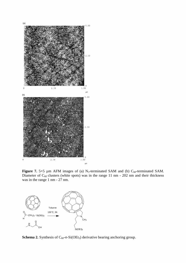
Surface topology of N3- and C60-terminated SAMs was compared by TM-AFM. As shown on
figure 7, N3-terminated SAM was very smooth with low rms roughness of 0.20 nm over 5×5
µm area close to supporting silicon wafer roughness. On the contrary, rms roughness of C60-
terminated SAM (1.07 nm) was more important with homogeneous repartition of C60
aggregates (10-200 nm diameter, 1-30 nm thick) as previously observed in literature on
various types of surfaces.16,30
It was not possible to eliminate these C60 clusters by sonication
in different solvents indicating that aggregates were strongly chemisorbed on the monolayer.
Actually high temperature grafting for several hours appeared to be inappropriate for these
low thickness monolayers contrary to certain successful examples from literature.16-17
High
temperature necessary for C60 grafting damaged monolayers and most of theses reactions
were difficult to reproduce.
2- Si/SiO2/σC60 molecular junction by direct grafting
Given difficulties of reproducibility observed with previous sequential methods, we
undertook direct grafting of preformed σ-C60 molecule bearing trialkoxysilyl anchoring group
on natively oxidized silicon. We carried out the synthesis of the fullerene derivative
represented on schema 2 following the previously described Prato method31
by reaction of N-
methylglycine and triethoxysilylbutyraldehyde with C60. In this fullerene derivative, -Si(OEt)3
group is attached at 2-position of the pyrrolidine ring through a short propyl spacer. It was
obtained in low yield (22 %) after purification by flash chromatography and was successfully
characterized by 1H and
13C NMR (see the supplementary information section).
Contrary to preceding sequential methods (realized above 80°C and damaging the SAM), self
assembly of the C60 derivative on natively oxidized silicon substrate required 4 days in soft
conditions (room temperature). Lower temperature should favor molecule organization in the
monolayer. Obviously, to compare with preceding sequential routes, one cannot expect to get
the same σ alkyl chains compactness at the bottom of the monolayer because of C60
hindrance. Bulky molecular structures have an important impact on the surface coverage :
generally, the bulkier the terminus, the lower the surface packing. Owing to that, in plane -Si-
O-Si- polysiloxane reticulation should be also less favored. As indicated in table 1, SAM
thickness measured by ellipsometry (14.4 Å) was in conformity with theoretical value (14.7
Å). Static water contact angle of C60 monolayer was 70°, in agreement with literature.17
Chemical composition of C60-functionalized SAM obtained by direct grafting was also
evaluated by XPS analysis. The measured C/N atomic ratio was about 44, i.e. 3.5 times higher
than in the case of sequential route 3, but the surface presented less carbon as can be
evidenced for example by comparing relative intensities of C1s and Si2p on fig. 4(b) and fig.

8. This is consistent with the fact that the σ moiety is denser in the case of SAM obtained by
sequential route 3, since it remains unreacted alkyl chains not linked to C60. In the case of
direct grafting, the high resolution spectra of N1s (see inset of fig. 8) and C1s (see fig. 9 solid
line) presented less chemically distinct environments compared to sequential route 3 (fig. 3(b)
and fig. 9 dashed line). The N1s core level, whose intensity was very low compared to
sequential route 3, presented only one component. As for the N1s core level peak, C1s
showed less asymmetry at higher binding energies (fig. 9) which means there were less
carbon atoms involved in bonds with oxygen atoms. The oxygen concentration in the case of
direct grafting mainly resulted from the silicon oxide of the substrate.
Figure 10 shows the voltammogram of C60-terminated SAM prepared in the same conditions
on two substrates: Si n+/SiO2 and ITO. As previously observed for sequential methods, a
reduction peak was observed at -1.11 V/SCE confirming surface functionalization by C60
electroactive species. This peak was better resolved on less resistive ITO substrate.
3- Electrical measurements of Si/SiO2/σC60//σHg molecular junction by direct grafting
We studied the electronic transport properties of the molecular junctions obtained by direct
grafting since we have shown above that the SAMs formed by this route were more
homogeneous and reproducible. To electrically characterize the molecular junction, we used
an electric contact by mercury drop on top of the SAM.32
This soft method avoids formation
of short circuit through the monolayer. By comparison with direct evaporation of metal, the
weak interactions between organic and metal avoid metal penetration in the organic
material.33
Another advantage of this method is the easy possibility to form a second σ tunnel
barrier by grafting an alkylthiol monolayer on the mercury drop. Here, Hg drop was thiolated
with two different alkyl chain lengths (C6 and C14 for short) by CH3(CH2)nSH alkylthiols
(with n=5 and n=13 respectively). Then Hg drop (with or without the alkylthiol SAM) was
gently contacted on the sample to define the two molecular junctions: Si/SiO2/σC60//Hg and
Si/SiO2/σC60//σHg, respectively (figure 11).
Current-voltage characteristics were measured on these junctions (figure 12) for various
lengths of the second tunnel barrier. We modified the length of the second barrier by changing
the SAM grafted on the mercury drop. In figure 12, three junctions were compared i) without
second tunnel barrier, i.e. the mercury drop directly in contact with C60, ii) with a thin
alkylthiol SAM (C6) grafted on mercury drop, and iii) with a thicker alkylthiol SAM (C14)
grafted on mercury drop. As expected, the current decreased with the increase of the second
tunnel barrier thickness. For example, at 1 V, the currents measured without second barrier,
with a C6 SAM, and with a C14 SAM are 8.6x10⁻⁸
A, 1.3x10⁻¹⁰
A and 3.9x10⁻¹²
A,
respectively. As expected, in the framework of a non-resonant tunneling transport through the
molecular junction, the current is exponentially dependent on the SAM thickness, and we
deduce a tunnel attenuation factor of 0.6±0.2 Å-1
. This value is as expected for a π conjugated
molecule,34
and similar to values reported for quite similar monolayer molecular junctions
made of a short oligomer (oligophenylene) in-between two alkyl chains.35
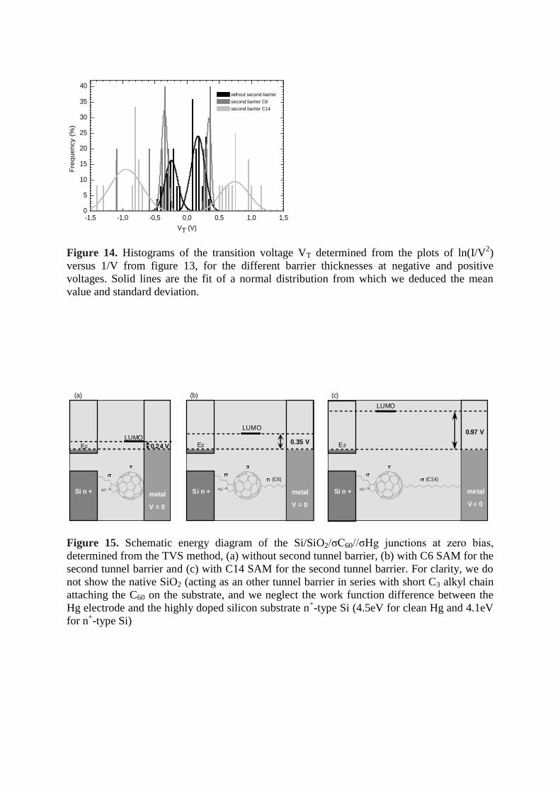
We analyzed the I-V traces by transition voltage spectroscopy (TVS) method.36
Recent works
have shown that the TVS method gives a good determination of the position of the molecular
orbitals with respect to the Fermi energy of the electrodes.37,38
Figure 13 shows the plots of
ln(I/V2) vs. 1/V for the same I-V data as in figure 12, for the negative and positive voltages.
The bias (VT) at the minimum of ln (I/V²) directly determines the energy offset Φ = e |VT|
between the Fermi energy in the electrodes and the frontier orbitals of the molecules.

The curves presented in the figure 13, show a clear difference for the VT as function of the
distance between the C60 and the Hg drop, i.e. as function of the thickness of the SAM grafted
on Hg drop. Without the second tunnel barrier the VT values for the negative and positive part
are respectively -0.22V and 0.24V. With the presence of the second tunnel barrier, the values
for VT increase to -0.40 and 0.40 with C6 SAM, -0.66 and 0.59 with a C14 SAM. This typical
example shows a clear tendency: the energy offset between the metal Fermi energy and the
molecular orbital (whether it is the LUMO or HOMO will be discussed below) decreases
when decreasing the coupling distance between the C60 and the Hg electrode.
This tendency was confirmed by recording between 5 and 25 I-V traces for each junction.
Figure 14 shows the dispersion of the measured current at 1 V probably due to
inhomogeneities in the molecular organization of the SAM. Two peaks of VT are observed for
each junction, corresponding to the negative and positive voltage. Without the second tunnel
barrier the mean VT value is equal to -0.24 ± 0.09 (this latter value is the standard deviation of
normal distribution shown in fig. 14) and 0.17 ± 0.10 for negative and positive bias,
respectively. These VT values increase with the thickness of the second tunnel barrier to -0.35
± 0.04 and 0.33 ± 0.03 for the C6 SAM, and to -0.97 ± 0.20 and 0.83 ± 0.18 for the C14
SAM. The slight difference of the values measured from the negative and positive biases can
be due to i) the slight difference in the work function of the Si and Hg electrodes, ii) the slight
geometrical asymmetry in the position of the C60 core in between the two electrodes due to
the different lengths of the σ spacers (note that the lowest asymmetry, -0.35 V and 0.33 V, is
obtained when these spacers are not too different, that is with C3 and C6 chains, respectively).
From these energy levels determined by the TVS method, we deduced the energy diagram for
each molecular junction (figure 15). We assumed that the VT value determined previously
corresponds to the energy position of the LUMO with respect to the Fermi energy of the
electrodes. This statement relies on two features: i) C60 is an acceptor molecule with an
electron affinity of about 2.7 eV and it is likely that charge transfer occurs via the LUMO, ii)
scanning tunneling experiments (STS) on single C60 deposited on H-passivated Si and slightly
oxidized Si have clearly detected such a resonant transport through the LUMO and not the
HOMO.39,40
The mean value of 0.83-0.97 eV measured here when the C60 is electronically
decoupled from both the Si and the Hg electrodes with alkyl chains is consistent with the
about 1 eV value reported with the STS experiments (in which the C60 is also decoupled from
the Si electrode by a thin SiO2 layer and by the vacuum gap between the tip and the
molecule)3 and also in agreement with ab-initio calculations.
41 Our results clearly illustrate
that increasing the electronic coupling between the molecule and the electrode, by decreasing
the chain length of the alkanethiol molecule, results, as expected, in a lowering of the LUMO
with respect to the Fermi energy of the electrode.42
4- Conclusion
The direct grafting of a presynthesized fullerosilane appeared to be the more efficient route to
prepare C60-based self assembled monolayer on natively oxidized silicon. Analysis of the I(V)
characteristics of Si/SiO2/σC60//Hg and Si/SiO2/σC60//σHg devices showed electron transport
through the LUMO of C60. By varying the length of the alkyl chain between the C60 core and
the Hg drop, we clearly observed the reduction of the energy offset between the LUMO and
the Fermi energy of the electrode when increasing the molecule-metal electronic coupling.

5- Experimental Section
Precursor SAMs bearing aldehyde, carbomethoxyaziridine and azide functions were prepared
by classical silanization reaction. The details of these syntheses and their physicochemical
characterizations are described in the supplementary information section.
C60-terminated SAM from N3-terminated SAM.
Glassware was dried in an air oven at 120°C overnight prior to use. The reaction was
performed in a reaction flask equipped with condenser and nitrogen inlet. N3-terminated SAM
was dipped into a degassed solution of C60 (20 mg) in anhydrous o-dichlorobenzene (20 mL).
The medium was refluxed at 180°C for 3 h under nitrogen atmosphere. After cooling, the
sample was removed from the solution, sonicated for 10 min in o-dichlorobenzene then in
chloroform, and finally blown with dry nitrogen.
C60-terminated SAM from carbomethoxyaziridine-SAM.
Carbomethoxyaziridine-terminated SAM was treated in similar conditions as N3-terminated
SAM. The medium was heated at 80°C for 24 h. In order to remove water traces in the
solvent, the reaction was performed in the presence of freshly activated molecular sieves (4
Å).
C60-terminated SAM from CHO-terminated SAM (Prato reaction).
The CHO-terminated surface was immersed in a degassed solution of C60 and N-
methylglycine in anhydrous o-dichlorobenzene at reflux for 16 h. After the reaction the
solution color changed from purple to dark red indicating formation of byproducts in the
medium. TLC analysis revealed the presence of several adducts in the solution. Sample was
removed from solution, sonicated 10 min in dichlorobenzene, chloroform, isopropanol and
then dried under nitrogen.
C60-terminated SAM by direct grafting.
Under the same conditions as for the synthesis of N3-terminated SAM, a freshly cleaned
silicon substrate was immersed for 4 days in a 10-3
M solution of N-methyl-2-(3-
triethoxysilylpropyl)-3,4-fulleropyrrolidine in anhydrous toluene. Sample was removed from
solution, sonicated 10 min in toluene then in chloroform, then dried under nitrogen.
Physicochemical characterizations of monolayers.
FT-IR spectra were recorded using a Perkin-Elmer Spectrum 2000 single-beam
spectrophotometer equipped with a tungsten-halogen lamp and a liquid nitrogen cooled MCT
detector. The functionalized silicon surfaces were characterized by reflection IR spectroscopy,
method also called attenuated total reflection (ATR).43
Static water contact angle measurements were done using a remote computer-controlled
goniometer system (DIGIDROP by GBX, France).
Spectroscopic ellipsometry data in the visible range was obtained using a UVISEL by Jobin
Yvon Horiba Spectroscopic Ellipsometer equipped with a DeltaPsi 2 data analysis software.
The system acquired a spectrum ranging from 2 to 4.5 eV (corresponding to 300-750 nm)
with 0.05 eV (or 7.5 nm) intervals. Data were taken using an angle of incidence of 70°, and
the compensator was set at 45.0°. To determine the monolayer thickness, we used the optical
properties of silicon and silicon oxide from the software library, and for the monolayer we
used the refractive index of 1.50. Usual values in the literature are in the range of 1.45-
1.50.18a,44
As a function of the wafer used, the oxide layer thickness was between 10 and 15 Å
(accuracy ±1 Å). The SiO2 thickness was assumed unchanged after monolayer assembly on

the surface. Accuracy of the SAM thickness measurements is estimated to be ±2 Å. All given
values for the reaction sequence were measured from a same silicon substrate.
X-ray photoemission spectroscopy (XPS) experiments were performed to control the
chemical composition of the SAMs and to detect any unremoved contaminant. Samples have
been analyzed by XPS, using a Physical Electronics 5600 spectrometer fitted in an UHV
chamber with a base pressure of about 3.10-10
Torr. The X-ray source was monochromatic Al
K (h = 1486.6 eV) and the detection angle was 45° with respect to sample surface normal.
Intensities of XPS core levels were measured as peak areas after standard background
subtraction according to the Shirley procedure.
Atomic force microscope measurements were conducted in ambient air using a tapping mode
AFM (Veeco, model Dimension 3100 Nanoscope).
Electrochemical investigations were carried out under nitrogen atmosphere, in anhydrous and
degassed dichloromethane containing 0.1 M of tetrabutylammonium hexafluorophosphate as
the supporting electrolyte. Pieces of functionalized silicon or ITO surfaces (5 mm × 10 mm)
were used as working electrodes and a platinum wire was used as counter electrode. Cyclic
voltammograms were recorded at 1 V.s-1
with a potentiostat (Voltalab PGZ301) controlled by
a computer. The potentials were measured versus a saturated calomel electrode (SCE).
etailed protocols of physicochemical characterizations of monolayers are available in the
supplementary information section.
Electrical characterizations of Si/SiO2/σC60//Hg and Si/SiO2/σC60//σHg molecular
junctions.
Measurements were performed at room temperature in a nitrogen purged glove box.
Calibrated mercury drops (99.9999 %, purchased from Fluka) were generated by a controlled
growth mercury electrode (CGME model from BASi). The contact area of the mercury drop
with the sample surface was evaluated to 1,6×10⁻³
cm2 with a microscope camera.
Si/SiO2/σC60//σHg molecular junction was prepared contacting Si/SiO2/σC60 junction with an
alkanethiol-protected mercury drop (for details, see supplementary information section).
Electrical transport through the SAMs was determined by measuring the current density vs
the applied direct current (dc) voltage with an Agilent 4155C picoampermeter. Voltage was
applied on the mercury drop, the silicon substrate being grounded.
1 (a) A. F. Hebard et al. Nature 1991, 350, 600-601. (b) P. M. Allemand et al. Science 1991,
253, 301-303. (c) M. S. Dresselhaus, G. Dresselhaus, and P. C. Eklund, Science of Fullerenes
and Carbon Nanotubes (Academic Press, New York, 1996). 2 Lai-Sheng Wang, J. Conceicao, Changming Jin and R.E. Smalley, Chem. Phys. Lett. 1991,
182, 5-11. 3 A. Skumanich Chem. Phys. Lett. 1991, 182, 486-490.
4 T. D. Anthopoulos, B. Singh, N. Marjanovic, N. S. Sariciftci, A. Montaigne Ramil, H. Sitter,
M. Cölle and D. M. de Leeuw, Appl. Phys. Lett. 2006, 89 (21), 213504. 5 L. Grüter, F. Cheng, T. T. Heikkilä, M.T. González, F. Diederich, C. Schönenberger and M.
Calame, Nanotechnology 2005, 16, 2143-2148. 6 H. S. Majumdar, J. K. Baral, R. Österbacka, O. Ikkala
and H. Stubb, Organic Electronics,
2005, 6, 188-192. 7 (a) S. S. Gayathri and A. Patnaik, Chem. Commun., 2006, 1977-1979. (b) A. Honciuc, A.
Jaiswal, A. Gong, K. Ashworth, C. W. Spangler, I. R. Peterson, L. R. Dalton, and R. M.
Metzger, J. Phys. Chem. B 2005, 109, 857-871. (c) S. Acharya, H. Song, J. Lee, P. S. Kwon,

J.-P. Lee, G. Yogendranath, Y. H. Kim, Y. H. Jang, T. Lee, S. Samal and J.-S. Lee, Organic
Electronics 2009, 10, 85-94. 8 M. Grobis, A. Wachowiak, R. Yamachika, and M. F. Crommiea, Appl. Phys. Lett. 2005, 86,
204102. 9 R. M. Metzger, J. W. Baldwin, W. J. Shumate, I. R. Peterson, P. Mani, G. J. Mankey, T.
Morris, G. Szulczewski, S. Bosi, M. Prato, A. Comito and Y. Rubin, J. Phys. Chem. B, 2003,
107, 1021. 10
H. Park, J. Park, A. K. L. Lim, E. H. Anderson, A. P. Alivisatos and P. L. McEuen, Nature
2000, 407, 57-60. 11
B. Li, C. Zeng, J. Zhao, J. Yang, J. G. Hou, and Q. Zhu, J. Chem. Phys. 2006, 124, 064709.
(b) Zeng, C. et al., Appl. Phys. Lett. 2000, 77, 3595. 12
(a) L. Patrone, S. Palacin, J. Charlier, F. Armand, J. P. Bourgoin, H. Tang, and S. Gauthier,
Phys. Rev. Lett. 2003, 91, 096802. (b) L. Patrone, S. Palacin, J.-P. Bourgoin, J. Lagoute, T.
Zambelli and S. Gauthier, Chem. Phys. 2002, 281, 325-332. (c) L. Venkataraman, Y. S. Park,
A. C. Whalley, C. Nuckolls, M. S. Hybertsen, and M. L. Steigerwald, Nano Lett., 2007, 7,
502-506. (d) A. Danilov, S. Kubatkin, S. Kafanov, P. Hedegård, N. Stuhr-Hansen, K. Moth-
Poulsen, and T. Bjørnholm, Nano Lett., 2008, 8, 1-5. (e) M. Kiguchi, O. Tal, S. Wohlthat, F.
Pauly, M. Krieger, D. Djukic, J. C. Cuevas, and J. M. van Ruitenbeek, Phys. Rev. Lett. 2008,
101, 046801. (f) Y. S. Park, A. C. Whalley, M. Kamenetska, M.L. Steigerwald, M. S.
Hybertsen, C. Nuckolls, and L. Venkataraman, J. Am. Chem. Soc., 2007, 129, 15768-15769.
Nano Letters 2008 8 (1), pp 1-5 13
S. Lenfant, D. Guerin, F. Tran Van, C. Chevrot, S. Palacin, J. P. Bourgoin, O. Bouloussa,
F. Rondelez, and D. Vuillaume, J. Phys. Chem. B, 2006, 110, 13947. 14
For an overview on various approaches for the immobilisation of C60 on surfaces see
Bonifazi, D. et al., Chem. Soc. Rev., 2007, 36, 390-414. 15
(a) X. Zhang and A. V. Teplyakov, Langmuir, 2008, 24 (3), 810-820. (b) K. Chen, W. B.
Caldwell, and C. A. Mirkin, J. Am. Chem. Soc. 1993, 115, 1193-1194. 16
V. V. Tsukruk, L. M. Lander and W. J. Brittain, Langmuir, 1994, 10, 996-999. 17
(a) F. Cattaruzza, A. Llanes-Pallas, A. G. Marrani, E. A. Dalchiele, F. Decker, R. Zanoni,
M. Prato and D. Bonifazi, J. Mater. Chem., 2008, 18, 1570- 1581. (b) M. Maggini and G.
Scorrano, J. Am. Chem. Soc. 1993,115, 9798-9799. 18
(a) A. Ulman, An Introduction to Ultrathin Organic Films: From Langmuir-Blodgett to
Self-Assembly; Academic Press: Boston, 1991. (b) B. J. Ravoo, D. N. Reinhoudt and S.
Onclin, Angew. Chem. Int. Ed. 2005, 44, 6282-6304. 19
(a) M. Maggini, G. Scorrano and M. Prato, J. Am. Chem. Soc. 1993, 115, 9798-9799. (b) M.
Prato, M. Maggini, Acc. Chem. Res. 1998, 31, 519-526. (c) K. Kordatos, M. Prato, E. Menna,
G. Scorrano and M. Maggini, Journal of Sol-Gel Science and Technology 2001, 22, 237-244. 20
A. Bianco et al. J. Am. Chem. Soc., 1997, 119, 7550-7554. 21
(a) M. Iglesias, B. Gomez-Lor and A. Santos, Journal of Organometallic Chemistry, 2000,
599, 8-17. (b) J.E. Capilla, J.J. Gomez-Hernandez, A. Sahuquillo, C. Bellavia-Lund, J.-C.
Hummelen, K.M. Keshavarz-Knd i, R. Gonzalez and F. Wudl, J. Phys. Chem. Solids 1997,
58, 1983-1990. 22
Y.-S. Shon, K. F. Kelly,
N. J. Halas and
T. R. Lee, Langmuir 1999, 15, 5329-5332.
23 R. R. Sahoo and A. Patnaik, Applied Surf. Sci. 2005, 245, 26-38.
24 MOPAC calculations were realized by ChemOffice from Cambridge Soft.
25 M.D. Porter, T.B. Bright, D.L. Allara and C.E.D. Chidsey, J. Am. Chem. Soc. 1987, 109,
3559. 26
D. Dattilo, L. Armelao, M. Maggini, G. Fois and G. Mistura, Langmuir 2006, 22, 8764-
8769.

27
M.-T. Lee and G. S. Ferguson, Langmuir 2001, 17, 762-767. 28
For an example of triazoline XPS spectra see A.G. Marrani et al., Electrochimica Acta
2008, 53, 3903-3909. 29
G. L'abbe, Chem. Rev., 1969, 69, 345-363. 30
R. R. Sahoo and A. Patnaik, Appl. Surf. Sci., 2005, 245, 26-38. 31
(a) M. Maggini, C. De Faveri, G. Scorrano, M. Prato, G. Brusatin, M. Guglielmi, M.
Meneghetti, R. Signorini, and Renato Bozio, Chem. Eur. J. 1999, 5, 2501-2510. (b) A.
Bianco, M. Maggini, M. Nogarole, and G. Scorrano, Eur. J. Org. Chem. 2006, 2934. 32
R.E. Holmlin, R. Haag, M.L. Chabinyc, R.F. Ismagilov, A.E. Cohen, A. Terfort, M.A.
Rampi, G.M. Whitesides, J. Am. Chem. Soc., 2001, 123, 5075-5085. 33
D.R. Jung and A.W. Czanderna. Crit Rev. Sol. St. Mat. Sci. 1994,19, 1. 34
A.Salomon et al., Comparison of electronic transport measurements on organic molecules.
Adv. Mat. 2003, 15 (22), 1881-1890. 35
E. Tran, C. Grave, G. M. Whitesides and M. A. Rampi, Electrochimica Acta 2005, 50,
4850-4856. 36
J.M. Beebe, B. Kim, J.W. Gadzuk, C.D. Frisbie and J.G. Kushmerick, Phys. Rev. Lett.
2006, 97 (2),
026801. 37
J.M. Beebe, B. Kim, C.D. Frisbie and J.G. Kushmerick, ACS Nano 2008, 2 (5), 827-832. 38
E.H. Huisman, C.M. Guédon, B.J. van Wees and S.J. van der Molen, Nano Lett. 2009, 9
(11), 3909-3913. 39
L. Bolotov, N. Uchida and T. Kanayama, J. Phys. Condens. Matter 2003, 15, S3065-S3081. 40 M.C. Hersam, N.P. Guisinger and J.W. Lyding, Nanotechnology 2000, 11, 70-76. 41
G.C. liang and A.W. Gosh, Phys. Rev. Lett. 2005, 95, 076403. 42
T. Vondrak, C.J. Cramer and X.-Y. Zhu, J. Phys. Chem. B 1999, 103 (42), 8915-8919. 43
N. Harrick, Internal Reflection Spectroscopy, Wiley-Interscience: New York, 1967. 44
N. Parikh, A. Allara, I. Ben Azouz and F. Rondelez, J. Phys. Chem. 1994, 98, 7577-7590.

N
(CH2)3
Si(OEt)3
CO2Me
Si
(CH2)3
O
On
OH
N
CO2Me
Si
(CH2)3
O
On
N
CO2Me
C60
o-DCB, 80°C
molecu lar sievestoluene3 days
(CH2)3
Si(OEt)3Si
(CH2)3
O
On
OH
OH
OH
Si
(CH2)3
O
On
C60
N-methylglycine
o-DCB, 180°C
NCH3
Sequencial route 1
Sequencial route 2
Sequencial route 3
toluene48 h
Si
(CH2)3
O
On
C60Si
(CH2)3
O
On
N3 N
o-DCB, 180°C
N3
(CH2)3
Si(OMe)3
OH to luene20 h
SiO2
Si n+
SiO2
SiO2
SiO2
Si n+
SiO2
Si n+
SiO2
Si n+
SiO2
Si n+
SiO2
Si n+
SiO2
Si n+
Si n+
Si n+
Schema 1. Sequential surface chemistry used to graft C60 covalently on natively oxidized
silicon

C60-SAM thickness (Å) contact angle (°)
exp. theo. exp. ref.15b,17,22
Route 1 : from CHO-SAM 16.0 15.6 44±2
65-76
Route 2 : from aziridine-SAM 15.4 - 44.0 15.8 71±2
Route 3 : from N3-SAM 14.0 14.6 55 - 70±2
Direct grafting 14.4 14.7 70±1
Table 1. Thickness and wettability of C60-terminated SAMs by different routes.
-2,0 -1,5 -1,0 -0,5 0,0
-200
-180
-160
-140
-120
-100
-80
-60
-40
-20
0
20
-1,02V
I(µ
A)
E(V)
(a)
-2,0 -1,5 -1,0 -0,5 0,0 0,5
-30
-25
-20
-15
-10
-5
0
5
I(µ
A)
E(V)
-1,25 V
(b)
Figure 1. Cyclic voltammogram of C60-terminated SAMs obtained by sequential route 2 on Si
n+/SiO2. Experimental conditions : CH2Cl2/NBu4PF6, WE: Si n
+/SiO2 (9.7Å)/C60-SAM, CE :
Pt, Ref : SCE, 1 V/s. (a) C60-SAM thickness corresponding to 1-2 monolayers of C60 (b) C60-
SAM thickness corresponding to 1 monolayer of C60.

2000220028003000
2000220028003000
98
99
100
N3 SAM
C60
SAM
tra
nsm
itta
nce
cm-1
2101
2869
2933
29272860
cm-1
Figure 2. FTIR spectra of of N3- and C60-terminated SAMs (sequential route 3).
Figure 3. High resolution XPS spectra of the nitrogen 1s core level from (a) N3- terminated
and (b) C60-terminated SAMs.

Figure 4. XPS survey spectra of (a) N3- and (b) C60- terminated SAMs synthesized by
sequential route 3.
-2,0 -1,5 -1,0 -0,5 0,0
-70
-60
-50
-40
-30
-20
-10
0
10
-1,01 V
-1,74 V
µA
/cm
2
E(V/SCE)
-1,31 V
Figure 5. Cyclic voltammogram of N3-terminated SAMs in a saturated solution of C60 in
toluene-CH2Cl2 (v/v 1:1). Experimental conditions: toluene-CH2Cl2/NBu4PF6, WE: Si n+/SiO2
(9.1Å)/N3-SAM, CE : Pt, Ref : SCE, 10 mV/s.

-2,0 -1,5 -1,0 -0,5 0,0
-100
-80
-60
-40
-20
0
20
N3-SAM
C60
-SAM on SiO2 run 1
C60
-SAM on SiO2 run 2
I(µ
A)
E(V/SCE)
-0,79 V
-0,88 V
(a)
-2,0 -1,5 -1,0 -0,5 0,0
-250
-200
-150
-100
-50
0
50
I(µ
A)
E (V/SCE)
-1,80 V
-1,01V
(b)
Figure 6. Cyclic voltammograms of N3- and C60-terminated SAMs obtained by sequential
route 3 on Si n+/SiO2 and ITO substrates. Experimental conditions : CH2Cl2/NBu4PF6, WE: Si
n+/SiO2 (9.7Å)/C60-SAM, CE : Pt, Ref : SCE, 1 V/s. (a) C60-SAM on Si n
+/SiO2 substrate (b)
C60-SAM on ITO substrate.
(a)
(b)
Figure 7. 5×5 µm AFM images of (a) N3-terminated SAM and (b) C60-terminated SAM.
Diameter of C60 clusters (white spots) was in the range 11 nm - 202 nm and their thickness
was in the range 1 nm - 27 nm.
(CH2)3
Toluene
NSi(OEt)3
CH3
O
H
HN
OH
O
Si(OEt)3
130°C, 5h
Schema 2. Synthesis of C60-σ-Si(OEt3) derivative bearing anchoring group.

Figure 8. XPS survey spectrum of C60-terminated surface obtained by direct grafting of
derivative 2. The inset shows the high-resolution spectrum of N1s.
Figure 9. High resolution XPS spectra of the carbon 1s core level from C60-terminated
surface obtained by direct grafting (solid line) and by sequential route 3 (dashed line)

-1,5 -1,0 -0,5 0,0
-25
-20
-15
-10
-5
0
5I(
µA
)
E(V/SCE)
direct synthesis on Si/SiO2
direct synthesis on ITO-1,11 V
Figure 10. Cyclic voltammogram of C60-terminated SAMs obtained by direct grafting on Si
n+/SiO2 and ITO substrates. Experimental conditions : CH2Cl2/NBu4PF6, WE: Si n
+/SiO2/C60-
SAM, CE : Pt, Ref : SCE, 1 V/s.
(a)
Hg
Si
(CH2)3
O
On
Si n+/ SiO2
N CH3
(b)
Hg
S S
S
S
S
S
S
S
S
'
Si
(CH2) 3
O
On
Si n+ / SiO2
N CH3
Figure 11. Electrical measurement of molecular junctions by mercury drop electrode. Non-
thiolated (a) and thiolated (b) Hg drop in a solution of alkanethiol in hexadecane (this solvent
covering the Hg drop does not evaporate and maintains a protection film during
measurements).

-1,5 -1,0 -0,5 0,0 0,5 1,0 1,5
1E-12
1E-11
1E-10
1E-9
1E-8
1E-7
without second barrier
second barrier C6
second barrier C14
Cu
rre
nt (A
)
Applied bias (V)
Figure 12. Current-voltage characteristics measured on Si/SiO2/σC60//σHg junctions for
various tunnel barrier on the Hg drop : C14, C6 and without SAM. The curves were smoothed
by the adjacent average method (here average with 10 neighbors). The evaluated contact area
of the mercury drop with the sample surface was around 1.6x10⁻³
cm2. Voltage was applied
on the mercury drop.
-10 -8 -6 -4 -2 0 2 4 6 8 10-28
-26
-24
-22
-20
without second barrier
second barrier C6
second barrier C14
ln (
I/V
²)
1/V (V-1)
Figure 13. Plots of ln(I/V2) versus 1/V from data in figure 12. The curves were smoothed by
the adjacent average method (here average with 10 neighbors). The transition voltage VT
(voltage at the minimum of the ln(I/V2) determines the energy offset, Φ = e |VT|, between the
Fermi energy of the metal electrodes and the molecular orbital involved in the charge
transport through the molecular junction.
-1,5 -1,0 -0,5 0,0 0,5 1,0 1,50
5
10
15
20
25
30
35
40
without second barrier
second barrier C6
second barrier C14
Fre
qu
en
cy (
%)
VT (V)
Figure 14. Histograms of the transition voltage VT determined from the plots of ln(I/V2)
versus 1/V from figure 13, for the different barrier thicknesses at negative and positive
voltages. Solid lines are the fit of a normal distribution from which we deduced the mean
value and standard deviation.
EF
LUMO
V = 0
Si n + metal
EF
LUMO
Si n +NH3C NH3C
(C6)
NH3C
(C14)
(a) (b) (c)
EF
LUMO
V = 0
Si n + metal
0.97 V
0.24 V0.35 V
V = 0
metal
Figure 15. Schematic energy diagram of the Si/SiO2/σC60//σHg junctions at zero bias,
determined from the TVS method, (a) without second tunnel barrier, (b) with C6 SAM for the
second tunnel barrier and (c) with C14 SAM for the second tunnel barrier. For clarity, we do
not show the native SiO2 (acting as an other tunnel barrier in series with short C3 alkyl chain
attaching the C60 on the substrate, and we neglect the work function difference between the
Hg electrode and the highly doped silicon substrate n+-type Si (4.5eV for clean Hg and 4.1eV
for n+-type Si)

Supporting information
Synthesis and electrical properties of fullerene-based molecular junctions
on silicon substrate
D. Guérin, S. Lenfant, S. Godey, D. Vuillaume
1- Synthesis of organosilanes
Chemicals.
Buckminsterfullerene C60 (sublimed, 99.9%), N-methylglycine (99 %), sulfuric acid (96 %),
hydrogen peroxide (30 % in water), sodium azide (99.5 %), adogen 464, tetrabutylammonium
hexafluorophosphate (99 %), anhydrous o-dichlorobenzene (99 %) were all purchased from
Sigma Aldrich. N-[3-(triethoxysilyl)propyl]-2-carbomethoxyaziridine (97 %),
triethoxysilylbutyraldehyde (90 %), 3-chloropropyltrimethoxysilane (95 %) were purchased
from Gelest. Chloroform (99.9 %) and dichloromethane (99.9 %) were obtained from
Scharlau. Anhydrous acetonitrile (99.8 %), toluene (99.9 %), ethyl acetate (99.5 %),
isopropanol (99.7 %) were purchased from Carlo Erba. These chemicals were used as
received without further purification, except dichloromethane and toluene that were distilled
over calcium hydride then stored over freshly activated molecular sieves. For water-sensitive
reactions, glassware was dried in an oven at 120 °C overnight prior to use.
1H and
13C NMR spectra were recorded with AC 300 Bruker instrument.
1H NMR spectra
were recorded at 300 MHz and 13
C NMR spectra at 75 MHz. Chemical shifts of NMR spectra
are reported in ppm and referenced to tetramethylsilane.
FTIR spectroscopy of synthesized 3-azidopropyltrimethoxysilane was realized using a
Perkin-Elmer Spectrum 2000 single-beam spectrophotometer by transmission IR
spectroscopy in a sodium chloride crystal cell.
3-azidopropyltrimethoxysilane
3-azidopropyltrimethoxysilane was synthesized following the procedure developed by Karl et
al.1 by reaction of sodium azide with 3-chloropropyltrimethoxysilane in the presence of
Adogen 464 catalyst. Let us precise that N3-terminated SAMs is often also prepared by
surface chemistry from halide-terminated monolayers2,3
but this method would have required
one more chemical step in the reaction sequence and thus one more risk of pollution and
decrease of yield.
All glassware was dried in an air oven at 120 °C overnight prior to use and the reaction was
performed under nitrogen atmosphere. A solution of 3-chloropropyltrimethoxysilane (2.5 mL,
13.71 mmol), sodium azide (1 g, 15.4 mmol) in dry acetonitrile was refluxed for 16 h under
stirring in the presence of the catalyst Adogen 464 (200 mg, 0.4 mmol). After filtration of the
precipitated salt, then evaporation of the solvent, the resulting oil was purified by distillation
under reduced pressure (0.5 Torr). The first fraction (below 40°C) containing the unreacted
J. Mater. Chem
halogenated precursor was eliminated then 3-azidopropyltrimethoxysilane was obtained at
80°C as a clear liquid in a yield of 60 % (1.7 g). Caution: due to the excess of instable and
highly toxic sodium azide, the oil should not be distilled to dryness. 1H NMR (300 MHz;
CDCl3; Me4Si; 20°C) : δH(ppm) 0.67 (2H, m, -CH2Si), 1.68 (2H, m, -CH2CH2CH2-), 3.24
(2H, t, 3JCH = 6.95 Hz, -CH2N3), 3.55 (9H, s, CH3O).
13C NMR (75.5 MHz; CDCl3; Me4Si;
20°C) : δC(ppm) 6.27, 22.41, 50.50, 53.67. FTIR (in CCl4) : λmax 2098.8 cm-1
(-N3).
N-methyl-2-(3-triethoxysilylpropyl)-3,4-fulleropyrrolidine
A solution of C60 (100 mg, 139 μmol), N-methylglycine (50 mg, 561 μmol), and
triethoxysilylbutyraldehyde (150 µL, 553 μmol) in toluene (50 mL) was heated to reflux for 5
h. The solvent was evaporated then the crude product was purified by flash chromatography
(SiO2, 40-63 μm) with toluene first to remove the unreacted C60, then with a mixture of
toluene/ethyl acetate v/v 9 :1. The fulleropyrrolidine was isolated as a brown solid (32 mg, 22
%) by filtration after dissolution in a minimum of toluene then precipitation by the addition of
acetonitrile. During the flash chromatography, 50 % of unreacted fullerene was also
recovered. Rf = 0.47 in toluene/ethyl acetate, v/v 9:1. 1H NMR (300 MHz; C6D6; Me4Si; 20
°C): δH(ppm) 0.85 (2 H, t, CH2Si), 1.18 (9 H, t, J = 6.9 Hz, CH3CH2O), 1.34-1.58 (4H, m,
CH2CH2CH2Si), 2.65 (3H, s, CH3N), 3.80 (6H, q, J = 6.9 Hz, CH3CH2O), 3.74 (1H, t, J = 5.55
Hz, CHCH2), 3.87-3.92 (1H, m, CH2 pyrrolidine), 4.34 (1H, d, J = 9.78 Hz, CH2 pyrrolidine).
13C NMR (75.5 MHz; C6D6; Me4Si; 20 °C): δC(ppm) 11.77, 15.71, 21.48, 34.62, 39.48, 58.47,
70.22, 70.76, 76.85, 78.11, 135.91, 136.31, 136.71, 137.66, 140.01, 140.14, 140.51, 140.58,
142.02, 142.06, 142.19, 142.39, 142.42, 142.46, 142.49, 142.50, 142.56, 142.58, 142.98,
143.01, 143.05, 143.44, 143.56, 144.72, 144.78, 144.94, 145.12, 145.51, 145.54, 145.57,
145.60, 145.65, 145.75, 145.77, 145.93, 145.94, 146.16, 146.26, 146.28, 146.36, 146.40,
146.52, 146.53, 146.59, 146.63, 146.75, 147.06, 147.31, 147.48, 147.52, 154.34, 154.95,
155.05, 157.19.
2- Synthesis of aldehyde, carbomethoxyaziridine and azide terminated SAMs
CHO-terminated SAM, carbomethoxyaziridine-terminated SAM and N3-terminated SAM
were successfully prepared by classical silanization reactions immersing a freshly cleaned
natively oxidized silicon substrate in a 10-3
M solution of the corresponding organosilane in
toluene for several days.
Silicon substrate cleaning method. Substrates used for electrical characterizations were n-
type degenerated silicon wafers purchased from Siltronix (resistivity of ~10-3
.cm) to avoid
any voltage drop during electrical measurements. For FTIR spectroscopy, ATR silicon
crystals (undoped) were used (45°, 10 mm × 5 mm × 1.5 mm). Surface of silicon substrates
were covered with native oxide (10-15 Å thick) providing a dense array (~5 × 10¹⁴
cm-2
) of
reactive hydroxyl groups (-OH), which are anchoring sites for the alkyltrialkoxysilane
molecules. All silicon substrates including ATR silicon crystals were first sonicated in
chloroform for 5 min then dried under nitrogen. The polished side of the wafers was cleaned
by ozonolysis for 30 min in a UV/ozone cleaner (wavelength at 185 and 254 nm). Then, the
samples were dipped into a freshly prepared piranha solution (H2SO4-H2O2 2:1 v/v) at 100 °C
for 15 min, were rinsed thoroughly with DI water then were dried under nitrogen stream.
Finally, cleaning was ended by additional ozonolysis for 30 min. Caution: the piranha
solution violently reacts with organic chemicals; consequently, it should be handled with
extreme care.

N3-terminated SAM
The reaction was carried out at room temperature in a glovebox under nitrogen atmosphere. A
freshly cleaned silicon substrate was immersed for 48 h in a 10-3
M solution of 3-
azidopropyltrimethoxysilane in anhydrous toluene (i.e. ~20 µL of organosilane in 20 mL of
solvent). The substrate was removed, sonicated 5 min in toluene then in chloroform, and
blown with dry nitrogen.
Carbomethoxyaziridine-terminated SAM
The SAM was prepared by treating the freshly oxidized silicon substrate with N-[3-
(triethoxysilyl)propyl]-2-carbomethoxyaziridine in the same conditions as N3-SAM. The
immersion duration in toluene was 3 days.
CHO-terminated SAM
Freshly cleaned silicon substrate was immersed for 3 days in a 10-3
M solution of
triethoxysilylbutyraldehyde in anhydrous toluene in the same conditions as N3-SAM.
As can be seen in table 1, precursor SAMs thicknesses measured by ellipsometry were
conform to theoretical values (MOPAC, PM3 optimization) calculated considering the
molecules in their all-trans conformation and almost standing perpendicular to the surface.
Measured water contact angles (see table 1) were slightly lower than those of analogous
monolayers published in literature. In the present work, the molecule lengths are much
smaller than those previously described, and it is known4 that SAM of short chains are more
disordered than long ones, thus explaining the lower contact angles.
Precursor SAMs thickness (Å) contact angle (°)
exp. theo. exp. ref.
CHO-SAM 7.0 7.8 67±1 805
Aziridine-SAM 12.0 12.1 55±1 NR
N3-SAM 8.0 8.8 68±1 776
Table 1. Thickness and wettability of precursor SAMs selected for sequential methods. NR :
no found reference in literature.
3- Instrumentation and methods for the physicochemical characterizations of self-
assembled monolayers
FTIR spectroscopy. FT-IR spectra were recorded using a Perkin-Elmer Spectrum 2000
single-beam spectrophotometer equipped with a tungsten-halogen lamp and a liquid nitrogen
cooled MCT detector. The functionalized silicon surfaces were characterized by reflection IR
spectroscopy, method also called attenuated total reflection (ATR).7 For the IR studies, all
substrates were ATR silicon crystals (45°, 10 mm×5 mm×1.5 mm). All measurements were
made after purging the sample chamber for 30 min with dry N2. Spectra were recorded at 4
cm-l resolution, and 200 scans were averaged. Background spectra of the freshly cleaned
crystal (with SiO2 layer) were recorded before any chemical treatment. After the chemical
reactions, the sample spectra were recorded in the same conditions. The monolayer
transmittance spectrum was obtained by dividing the sample spectrum by the background
spectrum.
J. Mater. Chem
Contact angle measurements were done using a remote computer-controlled goniometer
system (DIGIDROP by GBX, France). These measurements were carried out in a clean room
(class 1,000) where humidity, temperature, and pressure were controlled. Deionized water (18
M /cm) was used for these characterizations. Static drops (in the range 1-10 µL) of liquid
were applied to the modified surfaces with a micropipette and the projected image was
acquired and stored by the remote computer. Several measurements were taken on each
region of a given substrate. Contact angles were then extracted by contrast contour image
analysis software. These angles were determined 5 s after application of the drop.
Measurements made across the functionalized surfaces were within 2°.
Spectroscopic ellipsometry data in the visible range was obtained using a UVISEL by Jobin
Yvon Horiba Spectroscopic Ellipsometer equipped with a DeltaPsi 2 data analysis software.
The system acquired a spectrum ranging from 2 to 4.5 eV (corresponding to 300-750 nm)
with 0.05 eV (or 7.5 nm) intervals. Data were taken using an angle of incidence of 70°, and
the compensator was set at 45.0°. Data were fitted by regression analysis to a film-onsubstrate
model as described by their thickness and their complex refractive indices. First, before
monolayer deposition the silicon oxide thickness was measured. In the software, the measured
data were compared with the simulated data to determine this thickness. The simulated data
were obtained with a 2-layer model (Si/SiO2). In this model we use for the materials, the
optical properties (complex refractive index for each wavelength) from the software library.
Second, after the monolayer deposition we use a 3-layer model (Si/SiO2/organic film). To
determine the monolayer thickness, we use the oxide thickness previously measured, for
silicon and oxide we use the optical properties from the software library, and for the
monolayer we use the refractive index of 1.50. Usual values in the literature are in the range
of 1.45-1.50.8,9
One can notice that a change from 1.50 to 1.55 would result in less than 1 Å
error for a thickness less than 30 Å. As a function of the wafer used, the oxide layer thickness
was between 10 and 15 Å (accuracy ±1 Å). The SiO2 thickness is assumed unchanged after
monolayer assembly on the surface. Accuracy of the SAM thickness measurements is
estimated to be ±2 Å. All given values for the reaction sequence were measured from a same
silicon substrate.
X-ray photoemission spectroscopy (XPS) experiments were performed to control the
chemical composition of the SAMs and to detect any unremoved contaminant. Samples have
been analyzed by XPS, using a Physical Electronics 5600 spectrometer fitted in an UHV
chamber with a base pressure of about 3.10-10
Torr. The X-ray source was monochromatic Al
K (h = 1486.6 eV) and the detection angle was 45° with respect to sample surface normal.
Intensities of XPS core levels were measured as peak areas after standard background
subtraction according to the Shirley procedure.
Atomic force microscope measurements were conducted in ambient air using a tapping
mode AFM (Veeco, model Dimension 3100 Nanoscope) equipped with a silicon cantilever
(tip radius <20 nm).
Electrochemical investigations were carried out under nitrogen atmosphere, in anhydrous
and degassed dichloromethane containing 0.1 M of tetrabutylammonium hexafluorophosphate
as the supporting electrolyte. Pieces of functionalized silicon surfaces (5 mm × 10 mm) were
used as working electrodes and a platinum wire was used as counter electrode. Cyclic
voltammograms were recorded at 1 V.s-1
with a potentiostat (Voltalab PGZ301) controlled by
a computer. The potentials were measured versus a saturated calomel electrode (SCE). For
sequential route 3 and direct grafting, indium tin oxide substrates (ITO) were employed as

working electrodes instead of Si/SiO2 in order to amplify electrochemical signal. ITO was
first cleaned by sonication in chloroform for 5 min then treated by UV/ozone cleaner for 15
min before being functionalized exactly in the same conditions as Si/SiO2.
4- Experimental procedure for electrical characterizations of Si/SiO2/σC60//Hg and
Si/SiO2/σC60//σHg molecular junctions
Measurements were performed at room temperature in a nitrogen purged glove box. The Si
n+/SiO2/σC60 junctions were fixed onto copper substrates with silver paste. The wafer
backside was stripped with a diamond tip to remove backside oxide and ensure a good
electrical contact with the silver paste. These copper substrates were mounted onto a precision
vertical translation stage and the top contact was realized by carefully approaching the sample
surface towards a hanging mercury drop electrode. Mercury (99.9999 %) was purchased from
Fluka. Calibrated mercury drops were generated by a controlled growth mercury electrode
(CGME model from BASi). The contact area of the mercury drop with the sample surface
was evaluated to 1,6×10⁻³
cm2 with a microscope camera. Si/SiO2/σC60//σHg molecular
junction was prepared contacting Si/SiO2/σC60 junction with an alkanethiol-protected mercury
drop. This treatment was obtained by immersing a hanging mercury drop in a 10-3
M solution
of hexadecanethiol (C6) or tetradecanethiol (C14) in hexadecane for 18 h. The thiolated drop
was removed from the solution then directly applied on the Si/SiO2/C60 junction (see fig. 11).
During measurements, the mercury drop electrode is protected by a film of the alkylthiol
solution in hexadecane (this solvent does not evaporate). Electrical transport through the
SAMs was determined by measuring the current density vs the applied direct current (dc)
voltage with an Agilent 4155C picoampermeter. Voltage was applied on the mercury drop,
the silicon substrate being grounded.
1 A. Karl and W. Buder, 1983, US patent 4401598.
2 H. Park, J. Park, A. K. L. Lim, E. H. Anderson, A. P. Alivisatos and P. L. McEuen, Nature 2000, 407, 57-60.
3 T. Lummerstorfer and H. Hoffmann, J. Phys. Chem. B 2004, 108, 3963-3966.
4 S. R. Wasserman, Y. Tao and G. M. Whitesides, Langmuir 1989, 5, 1074-1087.
5 A. Hozumi, M. Inagaki and N. Shirahata Surface Science 2006, 600, 4044-4047.
6 J. P. Collman, N. K. Devaraj, T. P. A. Eberspacher and C. E. D. Chidsey, Langmuir 2006, 22, 2457-2464.
7 N. Harrick, Internal Reflection Spectroscopy, Wiley-Interscience: New York, 1967.
8 A. Ulman, An Introduction to Ultrathin Organic Films: From Langmuir-Blodgett to Self-Assembly; Academic
Press: Boston, 1991. 9 N. Parikh, A. Allara, I. Ben Azouz and F. Rondelez, J. Phys. Chem. 1994, 98, 7577-7590.
Recommended