www.sciencemag.org/cgi/content/full/335/6074/1330/DC1
Supporting Online Material for
Scaling Hetero-Epitaxy from Layers to Three-Dimensional Crystals Claudiu V. Falub,* Hans von Känel, Fabio Isa, Roberto Bergamaschini, Anna Marzegalli,
Daniel Chrastina, Giovanni Isella, Elisabeth Müller, Philippe Niedermann, Leo Miglio
*To whom correspondence should be addressed. E-mail: [email protected]
Published 16 March 2012, Science 335, 1330 (2012) DOI: 10.1126/science.1217666
This PDF file includes:
Materials and Methods SOM Text Figs. S1 to S12 References (32–36)
2
Materials and Methods
Substrate patterning Most of the 100 mm Si(001) substrates were patterned by conventional photolithography and deep reactive ion etching (DRIE) based on the Bosch process (32). This technique is widely used in microsystems fabrication. It provides very good anisotropy and high etch rate (~ several micrometers per minute) but rough sidewalls. We used patterns with uniformly spaced pillars, as well as pillars arranged in 10×10 blocks separated by wider trenches. In order to explore the influence of sidewall roughness on the epitaxial growth, a cryogenic process (33) was used for a number of substrates yielding smooth sidewalls. In addition to the usual patterns with clean pillar sidewalls and trench bottoms, some patterns received a passivating oxide coating (~90 nm SiO2), leaving only the top of the pillars oxide-free for epitaxial growth. Crystal growth Samples were grown by low-energy plasma-enhanced chemical vapor deposition (LEPECVD), a process based on an Ar plasma sustained by a low-voltage, magnetically confined direct-current arc discharge between a heated Ta filament and a ring anode in electrical contact with the grounded chamber walls. The potential distribution between the filament and the anode gives some directionality to the ionic species in the plasma, which in turn gives rise to the vertical component of the flux used in the modeling (27, 34). Pure germane (GeH4) is used as the reactive gas, while silane (SiH4) can also be added to deposit SiGe alloys of any composition. The base pressure in the load-locked growth chamber was below 110-9 mbar, whereas during growth the pressure was ~210-2 mbar. The nominal growth temperature, TG, was measured with thermocouples located behind the heater, and the correspondence between these temperature readings and the true substrate temperature was calibrated by means of an infrared pyrometer. However, since the substrate is directly exposed to a high-density plasma during deposition, the actual surface temperature is difficult to determine, and may differ from the calibration obtained by optical pyrometry in UHV. Prior to deposition, the patterned Si substrates were cleaned using the industry standard RCA method (35), and the native oxide was removed by a dilute (5%) HF dip and subsequent rinse in ultrapure water. Once loaded into the growth chamber, the substrates were outgassed in UHV for 15 min at 300C before ramping to the growth temperature. Analytical methods to investigate the surface morphology, dislocation density and crystalline quality of Ge towers The morphology of the Ge towers grown on the patterned Si substrates was monitored by Nomarski interference contrast optical microscopy (Nikon Eclipse 200D) and scanning electron microscopy (SEM) (Zeiss ULTRA 55 digital field emission). Facet orientation was accurately determined by atomic force microscopy (AFM) using a Veeco Innova microscope, and transmission and scanning electron microscopy (TEM, STEM) using a Tecnai F30ST TEM/STEM transmission electron microscope (FEI), operated at 300 kV. The specimens for TEM/STEM investigations were thinned to electron transparency by mechanical thinning followed by Ar-ion milling (acceleration voltage 4.3 kV, etching angle 4°, final polishing at 1 kV acceleration voltage).
3
Threading dislocations in Ge towers were inspected by TEM. The dark field STEM technique was used (in [110] zone axis orientation) to improve the visibility of dislocations in areas of high dislocation density by suppressing the contributions of bending contours and thickness fringes to the image contrast. Defect etching was used to estimate the dislocation density. The Ge towers were etched for 40 seconds in a diluted iodine solution (15 mg I2, 33 ml glacial acetic acid, 10 ml 65% nitric acid, 5 ml 40% HF, etch rate about ~10 nm/s) at 0°C. Etch pits were counted by AFM.
High-resolution x-ray diffraction (HRXRD) was used to investigate the crystalline quality and strain of the Ge towers. The HRXRD measurements, e.g. rocking curves, -2 scans and reciprocal space maps (RSMs), were performed with Cu K1 radiation using a PANalytical X’Pert Pro-MRD diffractometer equipped with a 4-bounce Ge(220) crystal monochromator on the incident beam, and an analyzer crystal and a Xe point detector on the diffracted beam. The x-ray beam diameter on the sample was ~1 mm. Therefore, depending on the lateral pattern dimensions, several thousands of Ge towers were probed simultaneously. To assess the tilt of individual Ge towers submicrometer diffraction experiments were performed at the ID01 beamline of European Synchrotron Radiation Facility (ESRF) in Grenoble, using an 11.07 keV x-ray beam focused down to ~300500 nm by means of Fresnel zone plates (FZP) and a Huber diffractometer equipped with a high-precision (x,y,z) stage. For a certain reflection, e.g. symmetric or asymmetric, and a fixed (x,y) position, the incidence angle of the x-ray beam was scanned while moving the beam across the sample. Since a 2D pixel detector was used, three-dimensional RSMs could be constructed for each (x,y) position of the x-ray beam on the sample.
Supporting Text Estimation of the separation of Ge towers Low resolution STEM micrographs were used to determine quantitatively the distance between the Ge towers as a function of their height. For ~7-μm-tall Ge towers grown at 440°C on an array of 8-μm-tall and 2-μm-wide Si pillars spaced by 4 μm trenches the result is presented in fig. S1. We see that after ~2 μm Ge deposition the lateral growth has become negligible, and, except for the top region exhibiting facets, the separation between the Ge towers remains constant at ~55 nm. A very similar self-limitation has been observed for much thinner deposits on top of narrowly spaced Si pillars (or mesas), as discussed below in conjunction with fig. S5. Whether the effect of full lateral growth suppression below a critical distance can be attributed to the low sticking probability of molecules on the {110} facets below a critical grazing angle of the incoming flux, or to the efficient downward diffusion of deposited material towards the trench bottom is not yet clear, and more detailed investigations are required. Ubiquity of epitaxial tower morphology The space-filling arrays of epitaxial crystals obtained by self-limited lateral growth on top of Si pillars were found to be remarkably independent of any detail of the fabrication procedure, as long as the basic conditions outlined in the text were fulfilled.
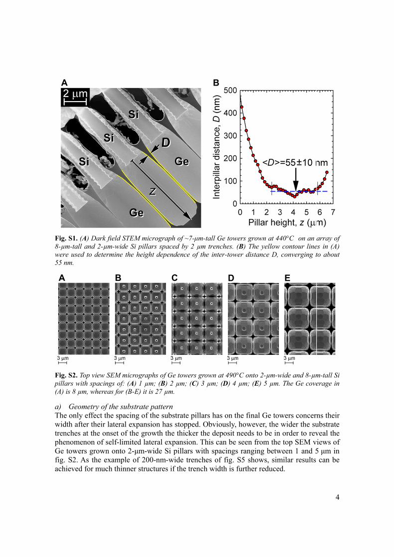
Fig. S8-µm-were 55 nm
Fig. Spillar(A) is
a) GThe owidthtrenchphenoGe tofig. Sachie
A
A
S1. (A) Dark-tall and 2-µused to dete
m.
S2. Top view rs with spacin 8 µm, where
Geometry ofonly effect th after their hes at the oomenon of owers grownS2. As the eeved for muc
k field STEM µm-wide Si permine the he
SEM microgngs of: (A) 1eas for (B-E)
f the substrathe spacing lateral expa
onset of the self-limitedn onto 2-μmexample of ch thinner s
B
micrograph pillars spacedeight depend
graphs of Ge 1 µm; (B) 2 µ it is 27 µm.
ate patternof the substansion has sgrowth the
d lateral expm-wide Si p200-nm-wi
structures if
C
of ~7-μm-tad by 2 µm tr
dence of the
towers growµm; (C) 3 µm
trate pillars stopped. Obthicker the ansion. This
pillars with ide trenchesthe trench w
C
ll Ge towers renches. (B)inter-tower d
wn at 490°C om; (D) 4 µm
has on the fbviously, hodeposit nees can be seespacings ra
s of fig. S5width is furt
B
D
grown at 44The yellow
distance D, c
onto 2-µm-wm; (E) 5 µm.
final Ge towwever, the w
eds to be in en from the anging betw
shows, simther reduced
40°C on an acontour lineconverging t
wide and 8-µmThe Ge cove
wers concernwider the suorder to revtop SEM v
ween 1 and 5milar results d.
E
4
array of
es in (A) to about
m-tall Si erage in
ns their ubstrate veal the
views of 5 μm in can be
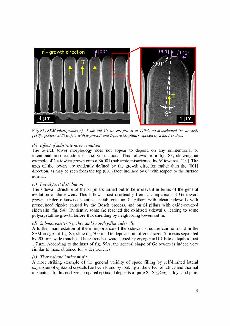
Fig. S[110]) (b) EThe intentexamaxes directnorm
(c) IThe sevolugrowpronosidewpolyc
(d) SA furSEMby 201.7 μsimil
(e) TA moexpanmism
S3. SEM mic), patterned S
Effect of suboverall towtional miso
mple of Ge toof the towtion, as may
mal.
Initial facet sidewall strution of the
wn, under oounced rippwalls (fig. Scrystalline g
Submicromerther manife
M images of 00-nm-wideμm. Accordiar to those o
Thermal andost strikingnsion of epi
match. To thi
crographs ofSi wafers wit
bstrate misower morphoorientation owers grow
wers are eviy be seen fr
distributionructure of the towers. Thotherwise idples caused S4). Evidentgrowth befor
eter trenchesestation of tfig. S5, sho
e trenches. Tng to the inobtained for
d lattice misg example oitaxial crystais end, we c
f ~8-µm-tall th 8-µm-tall
orientation ology doesof the Si s
wn onto a Si(idently defiom the top
n he Si pillarshis follows dentical con
by the Botly, some Gre flux shiel
s and smootthe unimpo
owing 500 nThese trenchnset of fig. r wider trenc
sfit of the geneals has been
compared ep
Ge towers gand 2-μm-wi
s not appeasubstrate. T(001) substrined by the(001) facet
s turned outmost drast
nditions, onosch procesGe reached lding by nei
th pillar sidortance of thnm Ge depohes were etcS5A, the geches.
eral validityn found by lpitaxial depo
grown at 44ide pillars, sp
ar to depeThis followrate misoriee growth diinclined by
t to be irreltically fromn Si pillars, and on Sthe oxidize
ighboring to
dewalls he sidewall sits on diffe
ched by cryoeneral shape
y of space looking at thosits of pure
0°C on misopaced by 2 μm
end on anyws from figented by 6° tirection rathy 6° with res
levant in term a comparirs with cleaSi pillars wed sidewallsowers set in.
structure caerent sized Sogenic DRIEe of Ge tow
filling by she effect of e Si, Si0.6Ge
oriented (6° m trenches.
y unintentiog. S3, showtowards [11her than thespect to the
rms of the ison of Ge an sidewall
with oxide-cs, leading to.
an be foundSi mesas seE to a depth
wers is indee
self-limited lattice and t
e0.4 alloys an
5
towards
onal or wing an
0]. The e [001] surface
general towers
ls with covered o some
d in the parated
h of just ed very
lateral thermal nd pure
Fig. Sµm-tapillar Ge, adjusS6, intower
Fig. S~1.7-µpillar(DRIEbetwe
A
S4. SEM micall and 2-µmrs with passiv
obtained usted to yieldndicates thar morpholog
S5. Perspectiµm-tall Si p
rs were fabricE). (A) 0.8-µeen two Ge to
crographs of -wide pillars
vated (~90-nm
under identid approximaat neither thgy in any sig
ive SEM micpillars with dcated by elecµm-wide Si powers); (B) 1
A
~8-µm-tall Gs, spaced by m-thick SiO2)
ical conditiately similarhe lattice mignificant wa
crographs of different aspctron beam lipillars (inset1.3-µm-wide p
B
Ge towers gr2 μm trenche) sidewalls.
ions, excepr surface diismatch noray.
f ~500-nm-tapect ratios sethography (Et shows a mpillars; (C) 1
B
rown at 560°es: (A) Si pil
pt for diffeffusion leng
r the therma
all self-limitedeparated byEBL) and cryagnified cros1.8-µm-wide
C on patternllars with cle
erent substrgths. The real mismatch
d Ge towers ~0.2-µm-wi
yogenic deepss-section SE
e pillars.
C
ned Si wafersean sidewalls
rate temperesult, shownh affect the
grown at 46ide trenches. reactive ionEM view of
6
s with 8- s; (B) Si
ratures, n in fig. general
60°C on The Si etching the gap
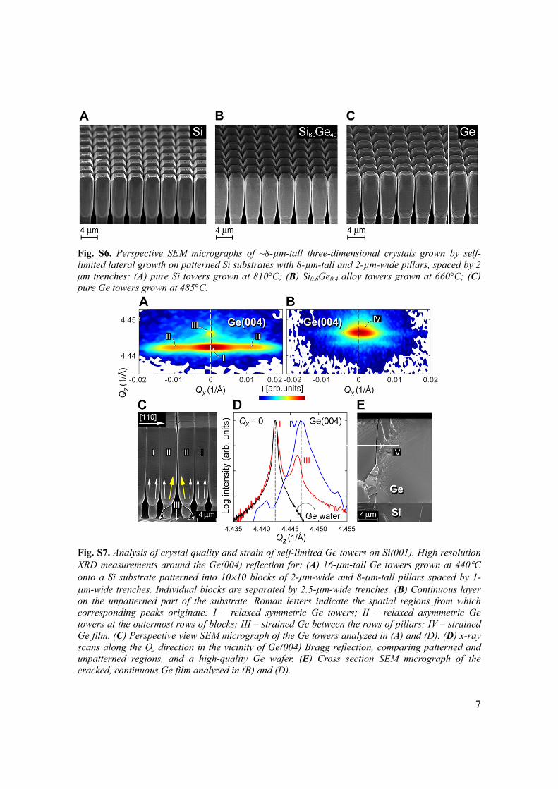
Fig. Slimiteμm trpure G
Fig. SXRD onto am-won thcorrestowerGe filscansunpatcrack
A
S6. Perspected lateral grorenches: (A) pGe towers gr
S7. Analysis measuremena Si substrat
wide trenchese unpatternesponding pers at the outelm. (C) Persps along the Qtterned regioked, continuo
tive SEM miowth on pattepure Si towe
rown at 485°
of crystal qunts around thte patterned
s. Individual ed part of theaks originatermost rows opective view Qz direction ions, and a hus Ge film an
icrographs oerned Si subsers grown atC.
uality and strhe Ge(004) r
into 1010 blocks are s
he substrate.te: I – relaxof blocks; IIISEM microgin the vicinityhigh-quality nalyzed in (B
B
of ~8-µm-talstrates with 8t 810°C; (B)
rain of self-lireflection forblocks of 2-eparated by Roman lett
xed symmetrI – strained Ggraph of the Gty of Ge(004)
Ge wafer. B) and (D).
ll three-dime8-µm-tall and Si0.6Ge0.4 al
imited Ge towr: (A) 16-mm-wide and2.5-m-wide
ters indicate ric Ge towerGe between tGe towers an) Bragg refle(E) Cross s
C
ensional crysd 2-µm-widelloy towers g
wers on Si(0m-tall Ge tow
d 8-m-tall pe trenches. (B
the spatial rs; II – relathe rows of pnalyzed in (Aection, compsection SEM
C
stals grown e pillars, spacgrown at 660
01). High res
wers grown apillars spaceB) Continuouregions from
axed asymmepillars; IV – sA) and (D). (Dparing pattern
M micrograph
7
by self-
ced by 2 0°C; (C)
solution at 440C ed by 1-us layer
m which etric Ge strained D) x-ray ned and h of the
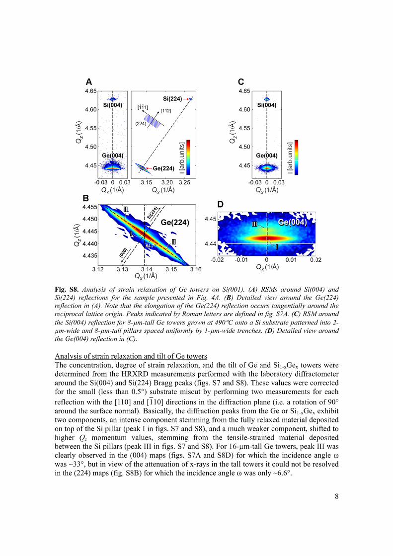
Fig. SSi(224reflecreciprthe Siµm-wthe G AnalyThe cdeterarounfor threflecarountwo con tohighebetweclearlwas ~in the
S8. Analysis4) reflection
ction in (A). Nrocal lattice i(004) reflect
wide and 8-µmGe(004) reflec
ysis of straiconcentratiormined fromnd the Si(00he small (lection with thnd the surfacomponentsop of the Si per Qz momeen the Si ply observed~33°, but ine (224) map
s of strain rs for the saNote that theorigin. Peakstion for 8-µmm-tall pillarsction in (C).
n relaxationon, degree o
m the HRXR04) and Si(2ess than 0.5he [110] an
ace normal).s, an intensepillar (peak
mentum valpillars (peakd in the (00n view of theps (fig. S8B)
relaxation of ample presene elongation ks indicated bm-tall Ge tows spaced unif
n and tilt of of strain relRD measure224) Bragg p5°) substratend [110] dire
Basically, te componentk I in figs. S7lues, stemmk III in figs. 4) maps (fie attenuatio) for which t
f Ge towers nted in Fig.
of the Ge(22by Roman letwers grown aformly by 1-µ
Ge towersaxation, and
ements perfopeaks (figs. e miscut byections in ththe diffractit stemming 7 and S8), a
ming from S7 and S8)
igs. S7A ann of x-rays the incidenc
on Si(001). 4A. (B) Det24) reflectiontters are defint 490C ontoµm-wide tren
d the tilt of formed with
S7 and S8)y performinghe diffractioion peaks frfrom the fu
and a much the tensile
). For 16-µmnd S8D) for
in the tall toce angle ω w
(A) RSMs atailed view an occurs tangned in fig. S7o a Si substranches. (D) D
f Ge and Si1
h the laborat). These valug two meason plane (i.erom the Ge ully relaxed
weaker come-strained mm-tall Ge to
which the owers it couwas only ~6
around Si(00around the Ggentially aro7A. (C) RSMate patterned
Detailed view
1-xGex towertory diffractues were cosurements foe. a rotationor Si1-xGex material de
mponent, shmaterial deowers, peak
incidence auld not be re6.6°.
8
04) and Ge(224) ound the
M around d into 2-
w around
rs were tometer orrected for each n of 90°
exhibit eposited hifted to eposited III was
angle ω esolved
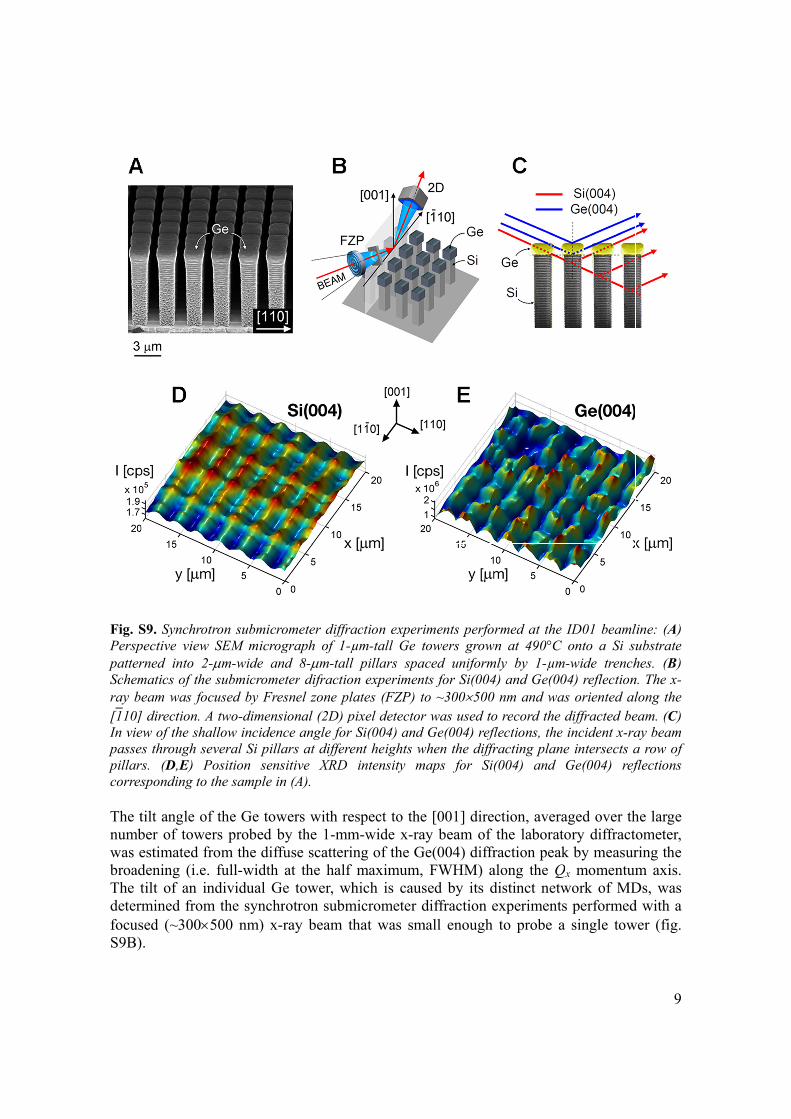
Fig. SPersppatterSchemray b[110]In viepassepillarcorres The tnumbwas ebroadThe tdeterfocusS9B)
S9. Synchrotpective view rned into 2-matics of the eam was foc
] direction. Aew of the shaes through sers. (D,E) Psponding to t
tilt angle ofber of towerestimated frdening (i.e. tilt of an in
rmined fromsed (~3005).
tron submicroSEM microg
-m-wide ansubmicrome
cused by FreA two-dimensallow incideneveral Si pillaPosition sens
the sample in
f the Ge towrs probed brom the diff
full-width ndividual Gm the synchr500 nm) x-
ometer diffragraph of 1-µ
nd 8-m-tall eter difractioesnel zone plsional (2D) pce angle for ars at differesitive XRD n (A).
wers with reby the 1-mmfuse scatterinat the half e tower, whrotron submray beam th
action experiµm-tall Ge tl pillars spaon experimenates (FZP) t
pixel detectorSi(004) and
ent heights wintensity m
espect to them-wide x-rang of the Gmaximum,
hich is causmicrometer dhat was sm
iments perfotowers grow
aced uniformnts for Si(004to ~300500 r was used toGe(004) refl
when the diffrmaps for Si(
e [001] direay beam of
Ge(004) diffrFWHM) a
sed by its ddiffraction e
mall enough
rmed at the n at 490°C
mly by 1-µm4) and Ge(00
nm and waso record the dflections, the fracting plane(004) and
ction, averathe laborato
raction peakalong the Qdistinct netwexperimentsto probe a
ID01 beamlonto a Si su-wide trench
04) reflections oriented aldiffracted beincident x-ra
e intersects aGe(004) ref
aged over thory diffractk by measur
Qx momentumwork of MDs performed single tow
9
line: (A) ubstrate hes. (B) n. The x-long the eam. (C) ay beam a row of flections
he large ometer, ring the m axis.
Ds, was d with a wer (fig.
In or490°Cfirst aunpatat difcovercan arelatifor Gone Son thacrosbelowobserexhibpillarGe(0a ranto the FiniteIn ordthe rCOM
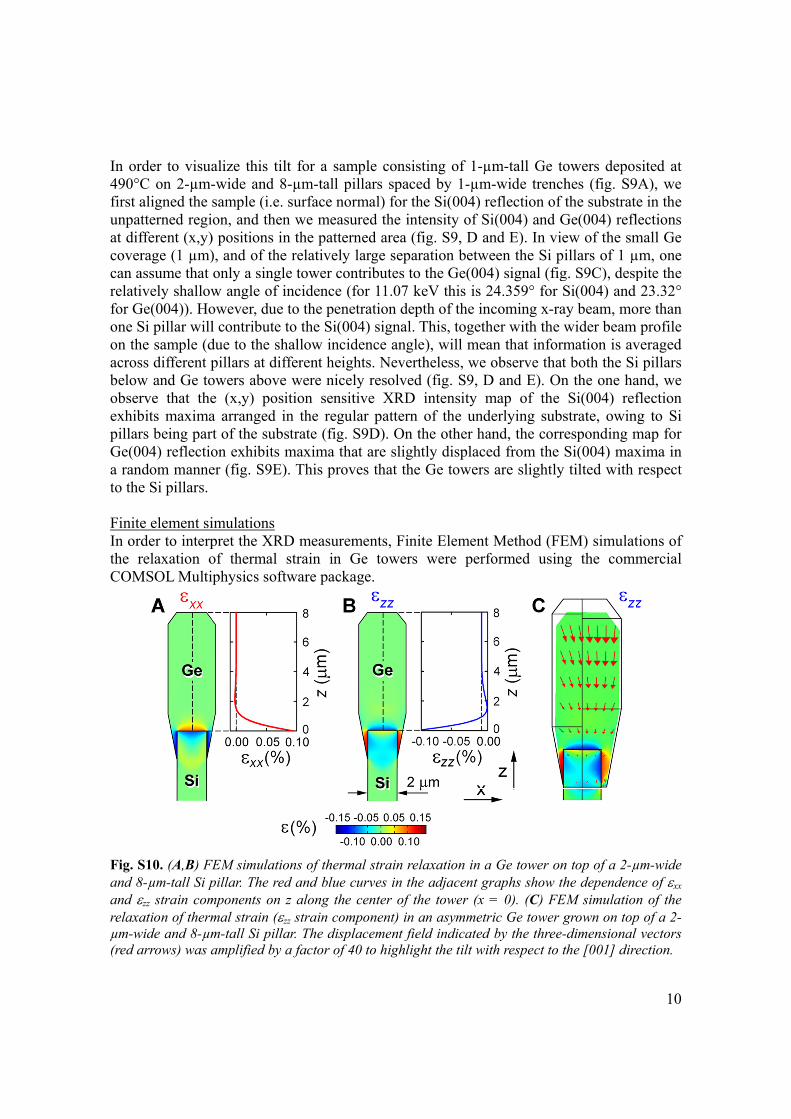
Fig. Sand 8and relaxaµm-w(red a
rder to visuaC on 2-µm-aligned the tterned regifferent (x,y)rage (1 µm)assume that ively shallow
Ge(004)). HoSi pillar willhe sample (dss different pw and Ge torve that thebits maximars being par04) reflectio
ndom mannee Si pillars.
e element sider to interprelaxation o
MSOL Multi
S10. (A,B) FE8-µm-tall Si pzz strain comation of therm
wide and 8-µmarrows) was a
alize this ti-wide and 8sample (i.e.ion, and then) positions i), and of theonly a singlw angle of owever, duel contribute due to the shpillars at difowers abovee (x,y) posa arranged irt of the subon exhibits er (fig. S9E)
imulations pret the XRof thermal iphysics soft
FEM simulatipillar. The remponents on mal strain (m-tall Si pillamplified by
lt for a sam8-µm-tall pi surface norn we measun the pattere relatively le tower conincidence (f
e to the peneto the Si(00
hallow incidfferent heige were nicelsition sensitin the regul
bstrate (fig. maxima tha). This prov
RD measuremstrain in G
ftware packa
ons of thermed and blue c
z along the zz strain comlar. The displa factor of 4
mple consistillars spacedrmal) for theured the interned area (filarge separa
ntributes to for 11.07 keetration dept04) signal. Tdence angle
ghts. Neverthly resolved tive XRD lar pattern S9D). On that are slightves that the
ments, FinitGe towers age.
mal strain relacurves in thecenter of th
mponent) in alacement fiel40 to highligh
ting of 1-µmd by 1-µm-e Si(004) reensity of Siig. S9, D anation betwethe Ge(004eV this is 24th of the incThis, togethee), will meanheless, we o(fig. S9, D intensity mof the undehe other hantly displacedGe towers
te Element Mwere perfo
axation in a adjacent gre tower (x =
an asymmetrild indicated bht the tilt with
m-tall Ge to-wide trencheflection of t(004) and G
nd E). In vieeen the Si pi) signal (fig4.359° for Scoming x-raer with the wn that informobserve that
and E). Onmap of the erlying subsnd, the corred from the Sare slightly
Method (FEormed using
Ge tower onaphs show th
= 0). (C) FEic Ge tower gby the three-h respect to t
owers depohes (fig. S9the substrat
Ge(004) reflew of the smillars of 1 µ
g. S9C), despSi(004) anday beam, mowider beammation is avt both the Sin the one haSi(004) ref
strate, owinesponding mSi(004) maxtilted with
EM) simulatg the comm
n top of a 2-µhe dependenc
EM simulatiogrown on top-dimensionalthe [001] dire
10
sited at 9A), we te in the lections mall Ge µm, one pite the
d 23.32° ore than
m profile veraged i pillars and, we flection
ng to Si map for xima in respect
tions of mercial
µm-wide ce of xx n of the p of a 2- l vectors rection.
11
For symmetric Ge towers grown on patterned Si substrates with constant spacing between the Si pillars, the simulated three-dimensional geometry consisted of a Si cylinder (2 µm in diameter and 8 µm in height) and a quadratic prism with a truncated pyramidal cap Ge tower on top (as tall as 8 µm), connected by a downward truncated pyramidal part, surrounding the Si cylinder. The numerical calculations were performed by meshing this geometry with 185200 elements and by considering an initial hydrostatic expansion in the Ge pillar equal to 0.20%, as derived from the difference in the thermal expansion coefficient of Si and Ge for a step in temperature ~500°C. As detailed in fig. S10, A and B, the strain components along a central axis of the Ge towers approach zero a few hundred nanometers above the Si/Ge interface.
To qualitatively confirm the tilt of the asymmetric Ge towers at the edge of the 10×10 blocks observed in the HRXRD RSM measurements (figs. S7 and S8), an asymmetric structure was analyzed by FEM simulations (see fig. S10C, where the map of the zz strain component is reported). Here we display also a magnified displacement pattern (red arrows), indicating that an actual tilting of the tower is qualitatively predicted. Additional remarks on the growth model For the two-dimensional simulations of the morphological evolution with deposition, we considered the following rate equations of the adatom density N for each small segment of a facet:
ΦC D
C ,
where is the site-dependent incident flux, C⁄ is the facet-dependent rate of crystallization (that is, the facet growth velocity ), and D⁄ is the rate of desorption/etching of adatoms from the surface toward the gaseous phase. Actually, C and
D are the respective adatom lifetimes, the former depending on the facet, the latter taken to be the same for each facet.
From the experimental SEM profiles for an isolated pillar at fixed growth temperature, starting from ~1 μm Ge deposition, we observe that the growth almost preserves the ratios between the growth velocities of the different facets. This is particularly evident in the linear trajectories of the vertices between the facets (dashed white lines in Fig. 3C). We can consider the system to be in a stationary state, and use the simplified equations reported below. This also means disregarding the process of initial facet nucleation, which cannot be treated by the model, but turns out to be irrelevant for the experimental tower morphology, as discussed in a previous section.
Under stationary conditions, the rate equations for each segment can therefore be written as:
0 ΦC D
Φ
C CΦ ∙ Φ,
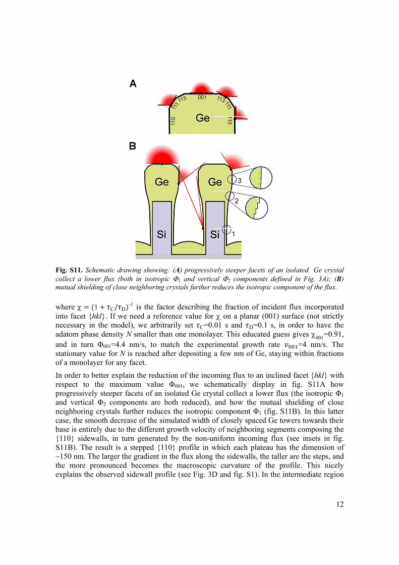
Fig. Scollecmutua
wherinto fnecesadatoand istatioof a m
In ordrespeprogrand vneighcase, base {110S11B~150the mexpla
S11. Schemact a lower flal shielding o
re 1facet {hkl}.ssary in theom phase dein turn Φ00
onary value monolayer f
der to betterect to the ressively stevertical Φ2 hboring crys
the smoothis entirely d} sidewalls
B). The resu0 nm. The lamore pronoains the obs
atic drawing flux (both in of close neigh
C/ D-1 is
If we neede model), wensity N sm
01=4.4 nm/sfor N is rea
for any facet
r explain thmaximum
eeper facetscomponent
stals furtherh decrease odue to the di, in turn ge
ult is a steparger the graounced becoerved sidew
showing: (Aisotropic
hboring crys
the factor dd a referenc
we arbitrarilymaller than o
s, to matchached after t.
he reductionvalue Φ00
s of an isolats are both r reduces th
of the simulaifferent growenerated byped {110}
adient in theomes the m
wall profile
A) progressiv1 and vertic
tals further r
describing tce value for y set C=0.
one monolayh the experdepositing
n of the inco01, we schated Ge crys reduced),
he isotropic ated width owth velocity
y the non-unprofile in w
e flux along macroscopic(see Fig. 3D
vely steeper fal 2 compo
reduces the is
the fraction on a plan
01 s and Dyer. This edrimental groa few nm o
oming flux thematically stal collect and how thcomponent
of closely spy of neighboniform inco
which each the sidewal
c curvatureD and fig. S
facets of an onents definsotropic comp
of incidentnar (001) suD=0.1 s, in
ducated guesowth rate
of Ge, stayin
to an inclinedisplay in
a lower fluxhe mutual t Φ1 (fig. Spaced Ge tooring segmeoming flux plateau has
lls, the tallere of the prS1). In the in
isolated Geed in Fig. 3
mponent of the
t flux incorpurface (not order to h
ss gives 00
=4 nm/ng within fr
ed facet {hkn fig. S11Ax (the isotroshielding o11B). In thi
owers towardents compos(see insets
s the dimenr are the sterofile. This ntermediate
12
e crystal 3A); (B) e flux.
porated strictly ave the
01=0.91, /s. The ractions
kl} with A how opic Φ1
of close is latter ds their sing the
in fig. nsion of eps, and
nicely e region
of thincomtowerpart oincomIn oustopsare jmorp
For tdiffusdrivebetweshortthen b
in whfacet-s coo
Fig. Sdiffus
he tower sidming flux surs was criticof the towerming flux wur model wes the lateral just the re
phology.
the higher gsion betwee
en by N gradeen facets. er, or at bebe re-writte
ΦC
hich the las-dependent
ordinate alon
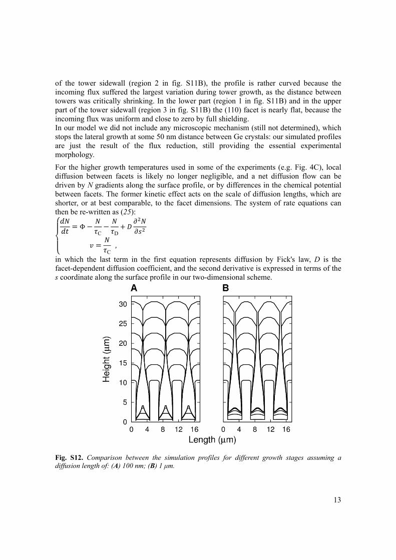
S12. Compasion length of
dewall (reguffered the cally shrinkr sidewall (r
was uniform e did not incgrowth at so
esult of the
growth tempen facets isdients alongThe former
est comparaben as (25):
D
C ,
st term in tdiffusion co
ng the surfac
arison betwef: (A) 100 nm
ion 2 in figlargest vari
king. In the region 3 in and close toclude any mome 50 nm e flux redu
peratures uss likely no g the surfacr kinetic effble, to the
the first eqoefficient, ace profile in
een the simum; (B) 1 μm.
g. S11B), tiation durinlower part fig. S11B)
o zero by fumicroscopic
distance beuction, stil
sed in somelonger negle profile, or
fect acts on facet dimen
quation reprand the secon our two-di
ulation profil
the profile ng tower gro
(region 1 inthe (110) fa
ull shieldingmechanism
etween Ge cl providing
e of the expligible, andr by differenthe scale o
nsions. The
esents diffuond derivativimensional s
les for diffe
is rather cuowth, as then fig. S11Bacet is nearl.
m (still not dcrystals: ourg the essen
periments (ed a net diffunces in the f diffusion system of
usion by Five is expresscheme.
erent growth
urved becaue distance b
B) and in thely flat, beca
determined)r simulated pntial experi
e.g. Fig. 4Cfusion flow
chemical plengths, whrate equatio
ick's law, Dssed in term
stages assu
13
use the between e upper
ause the
, which profiles imental
C), local can be otential
hich are ons can
D is the s of the
uming a
14
Our results for 2-µm-wide Si pillars, spaced 4 µm apart, are displayed in fig. S12A, using kinetic parameters extracted from the experimental evolution of an isolated tower and a diffusion length of the order of 100 nm (essentially no diffusion). By considering now the diffusion length inside each facet to be of order of 1 µm, comparable to the facet dimensions (still artificially keeping the same incorporation factors as for the previous case), we obtain both a retarded lateral growth and an expanding {111} top facet (fig. S12B). The growth of {111} facets at the expense of {113} facets is not, however, consistent with the experiments showing the opposite trend (Fig. 4C), so we conclude that even at the higher growth temperature diffusion is limited to a few hundred nanometers. Still, the experimental distribution of Ge material at the bottom of the trenches (Fig. 3D), seems to be smoother than our simulations with no diffusion and more consistent with the simulations based on a micrometer-sized diffusion length (fig. S12B). This observation supports the argument that by lowering the incoming flux (as happens at the bottom of the trenches) the diffusion is increased to common values expected for low rate depositions. Having explained the observed tower morphology in terms of kinetic (independent facet growth by short diffusion lengths) and geometric (mutual flux shielding) features, the question arises as to what extent the results remain valid for growth techniques other than LEPECVD. Clearly, some degree of flux shielding is always expected since in reality an in-plane flux component is present even for rather collimated particle beams, such as those in MBE. Still, since growth rates in MBE are generally much lower, either a surfactant or much lower substrate temperatures would have to be used, in order to guarantee short surface diffusion lengths (36).
1
References and Notes 1. V. Umansky et al., MBE growth of ultra-low disorder 2DEG with mobility exceeding
35×106 cm2/Vs. J. Cryst. Growth 311, 1658 (2009). doi:10.1016/j.jcrysgro.2008.09.151
2. H. L. Störmer, D. C. Tsui, The quantized Hall effect. Science 220, 1241 (1983). doi:10.1126/science.220.4603.1241 Medline
3. S. E. Thompson et al., A logic nanotechnology featuring strained-silicon. IEEE El. Dev. Lett. 25, 191 (2004). doi:10.1109/LED.2004.825195
4. J. H. van der Merwe, Crystal interfaces. Part II. Finite overgrowths. J. Appl. Phys. 34, 123 (1963). doi:10.1063/1.1729051
5. J. W. Matthews, S. Mader, T. B. Light, Accommodation of misfit across the interface between crystals of semiconducting elements or compounds. J. Appl. Phys. 41, 3800 (1970). doi:10.1063/1.1659510
6. J. W. Matthews, A. E. Blakeslee, S. Mader, Use of misfit strain to remove dislocations from epitaxial thin films. Thin Solid Films 33, 253 (1976). doi:10.1016/0040-6090(76)90085-7
7. P. D. Hodson et al., The growth of GaAs and LnxGa1–xAs on patterned silicon substrates. Semicond. Sci. Technol. 3, 715 (1988). doi:10.1088/0268-1242/3/7/013
8. E. A. Fitzgerald et al., Totally relaxed GexSi1−x layers with low threading dislocation densities grown on Si substrates. Appl. Phys. Lett. 59, 811 (1991). doi:10.1063/1.105351
9. E. A. Fitzgerald, N. Chand, Epitaxial necking in GaAs grown on pre-pattemed Si substrates. J. Electron. Mater. 20, 839 (1991). doi:10.1007/BF02665973
10. For a review of early work, see also (31).
11. M. R. Goulding, The selective epitaxial growth of silicon. Mater. Sci. Eng. B 17, 47 (1993). doi:10.1016/0921-5107(93)90080-7
12. H. C. Luan et al., High-quality Ge epilayers on Si with low threading-dislocation densities. Appl. Phys. Lett. 75, 2909 (1999). doi:10.1063/1.125187
13. T. A. Langdo et al., High quality Ge on Si by epitaxial necking. Appl. Phys. Lett. 76, 3700 (2000). doi:10.1063/1.126754
14. H. Klapper, Generation and propagation of dislocations during crystal growth. Mater. Chem. Phys. 66, 101 (2000). doi:10.1016/S0254-0584(00)00342-4
15. J.-S. Park et al., Defect reduction of selective Ge epitaxy in trenches on Si(001) substrates using aspect ratio trapping. Appl. Phys. Lett. 90, 052113 (2007). doi:10.1063/1.2435603
16. J. Bai et al., Study of the defect elimination mechanisms in aspect ratio trapping Ge growth. Appl. Phys. Lett. 90, 101902 (2007). doi:10.1063/1.2711276
2
17. S. Hu, P. W. Leu, A. F. Marshall, P. C. McIntyre, Single-crystal germanium layers grown on silicon by nanowire seeding. Nat. Nanotechnol. 4, 649 (2009). doi:10.1038/nnano.2009.233 Medline
18. G. Wang et al., High quality Ge epitaxial layers in narrow channels on Si(001) substrates. Appl. Phys. Lett. 96, 111903 (2010). doi:10.1063/1.3360231
19. E. Feltin et al., Stress control in GaN grown on silicon (111) by metalorganic vapor phase epitaxy. Appl. Phys. Lett. 79, 3230 (2001). doi:10.1063/1.1415043
20. M. Sakai, T. Egawa, M. Hao, H. Ishikawa, Effect of various interlayers on epiwafer bowing in AlGaN/GaN high-electron-mobility transistor structures. Jpn. J. Appl. Phys. 43, 8019 (2004). doi:10.1143/JJAP.43.8019
21. Y.-W. Mo, D. E. Savage, B. S. Swartzentruber, M. G. Lagally, Kinetic pathway in Stranski-Krastanov growth of Ge on Si(001). Phys. Rev. Lett. 65, 1020 (1990). doi:10.1103/PhysRevLett.65.1020 Medline
22. G. A. Slack, S. F. Bartram, Thermal expansion of some diamondlike crystals. J. Appl. Phys. 46, 89 (1975). doi:10.1063/1.321373
23. Materials and methods and supporting text are available on Science Online.
24. C. Rosenblad et al., Silicon epitaxy by low-energy plasma enhanced chemical vapor deposition. J. Vac. Sci. Technol. A 16, 2785 (1998). doi:10.1116/1.581422
25. M. Ohtsuka, S. Miyazawa, Model for molecular-beam-epitaxy growth over nonplanar surfaces. J. Appl. Phys. 64, 3522 (1988). doi:10.1063/1.341490
26. S. Li, Q. Xiang, D. Wang, K. L. Wang, Modeling of facet growth on patterned Si substrate in gas source MBE. J. Cryst. Growth 157, 185 (1995). doi:10.1016/0022-0248(95)00406-8
27. M. Rondanini et al., An experimental and theoretical investigation of a magnetically confined dc plasma discharge. J. Appl. Phys. 104, 013304 (2008). doi:10.1063/1.2948927
28. S. H. Jones, L. K. Seidel, K. M. Lau, M. Harold, Patterned substrate epitaxy surface shapes. J. Cryst. Growth 108, 73 (1991). doi:10.1016/0022-0248(91)90355-9
29. E. P. Kvam, D. M. Maher, C. J. Humphreys, Variation of dislocation morphology with strain in GexSi1−x epilayers on (100)Si. J. Mater. Res. 5, 1900 (1990). doi:10.1557/JMR.1990.1900
30. G. R. Booker et al., Nature, origin and effect of dislocations in epitaxial semiconductor layers. J. Cryst. Growth 45, 407 (1978). doi:10.1016/0022-0248(78)90470-0
31. A. Madhukar, Growth of semiconductor heterostructures on patterned substrates: defect reduction and nanostructures. Thin Solid Films 231, 8 (1993). doi:10.1016/0040-6090(93)90701-P
32. F. Laermer, A. Schilp, U.S. Patent 5501893_3, 26 (1996).
3
33. S. Tachi, K. Tsujimoto, S. Okudaira, Low-temperature reactive ion etching and microwave plasma etching of silicon. Appl. Phys. Lett. 52, 616 (1988). doi:10.1063/1.99382
34. M. Kummer et al., Low energy plasma enhanced chemical vapor deposition. Mater. Sci. Eng. B 89, 288 (2002). doi:10.1016/S0921-5107(01)00801-7
35. W. Kern, D.A. Puotinen, RCA Rev. 31, 187 (1970).
36. M. Copel, M. C. Reuter, E. Kaxiras, R. M. Tromp, Surfactants in epitaxial growth. Phys. Rev. Lett. 63, 632 (1989). doi:10.1103/PhysRevLett.63.632 Medline
Recommended


![WELCOME [cis.unimelb.edu.au]€¦ · Prof. Dr. Jürg von Känel from IBM, Dr. Kendra Vant from Seek and Chris Lewin from Deloitte were invited to provide their valuable guidance and](https://img.pdfslide.us/doc/110x75/5f01c2e67e708231d400e8fd/welcome-cis-prof-dr-jrg-von-knel-from-ibm-dr-kendra-vant-from-seek-and.jpg)