Study of the Properties of the Porous Silicon Synthesized by Ag Assisted Electrolysis Etching
Madhavi Karanam1,a, Mohan Rao G.2,*,b, Habibuddin Shaik3,c and Padmasuvarna R.1,d
1Department of Physics, Jawaharlal Nehru Technological University, Anantapur, India 560001
2Department of Applied Physics & Instrumentation, IndianInstitute of Science, Bangalore, India 560012
3Department of Physics, Nitte Meenakshi Institute of Technology, Bangalore, India 515002
[email protected], [email protected],[email protected], [email protected]
Keywords: Porous Silicon (PSi), Ag Nano particles, etching solution (HF,H2O2), Metal assisted chemical etching, Contact angle.
Abstract. Porous Silicon (PSi) is synthesized by Ag assisted electroless etching and characterized
by Scanning electron microscopy (SEM). The effect of etching time on the optical reflectivity,
optical absorbance of PSi is investigated. Reflectivity measurements showed gradual decrease in the
reflectivity with respect to etching time. 45% reflectivity of bare silicon drops to 10% for 2 hours
etching and to 6% for 3 hours etching. The decrease in the reflectivity shows that the PSi can be
employed as an anti reflecting substrate in optoelectronic devices. The absorbance measurements
revealed that the average absorbance of PSi is 0.60 in the wavelength range 300-800 nm after
2 hours etching. From the photoluminescence spectra it was found that PL intensity of PSi is high
compared to bare silicon wafer. Static water contact angle measurements were performed to
examine the hydrophobic properties of the PSi prepared under different conditions. The porous
silicon surface after etching has been demonstrated to be suitable for self cleaning applications.
1. Introduction
Porous silicon (PSi) has been under special investigation in the past decade due to wide
spectrum of applications in Optoelectronics [1-3] and in Chemical and Bio chemical sensors [4-7].
PSi is normally prepared by anodic etching [2], electrochemical etching (ECE) and stain etching.
The ECE method is cost inefficient in wafer scale [8] where as stain etching is slow and it is useful
in preparing the pores of few nano meters only[9]. The drawbacks of the above methods are
compensated by new method called metal assisted chemical etching (MACE). MACE is purely
solution based method used to produce uniform porous silicon layer very rapidly without any
external biasing. The method we adopted is two step MACE in which in the first step noble metal
layers (Ag, Au, Pt, etc.) are deposited on the Si wafer by various techniques such as sputtering [10],
electrochemical [11] or electroless displacement [12] and in the second step noble particles covered
silicon (Si) is etched in the solution containing Hydrofluoric Acid (HF) and an oxidizing agent. The
Silicon below the noble metal is etched faster than without noble metal [13]. Due to this, PSi layer
is formed within few seconds and can be controlled by the morphology of the deposited noble
metal. Also PSi fabrication is influenced by many MACE parameters like etching time,
temperature, concentration of etching solution etc. [14].
The motivation for this work is towards developing self cleaning surfaces. This could be
achieved by making a superhydrophobic surface. In this paper, a detailed report is given on the
fabrication of PSi using two step MACE known as Ag assisted chemical etching with silver (Ag) as
the noble particle and hydrogen peroxide (H2O2) as an oxidizing agent as a function of etching time.
We then provide an analysis on the optical and wettability properties of PSi indicating necessary
conditions for PSi to be used as antireflecting coatings and also as non-wetting surfaces.
International Letters of Chemistry, Physics and Astronomy Submitted: 2016-04-15ISSN: 2299-3843, Vol. 71, pp 40-48 Revised: 2016-08-26doi:10.18052/www.scipress.com/ILCPA.71.40 Accepted: 2016-09-02© 2016 SciPress Ltd., Switzerland Online: 2016-11-30
SciPress applies the CC-BY 4.0 license to works we publish: https://creativecommons.org/licenses/by/4.0/
2. Materials and Methods
2.1 Material
One side polished p-type (100) oriented silicon (Si) wafer with a resistivity of 1-10 Ωcm,
Silver nitrate AgNO3(0.02M), Nitric acid (HNO3), and Hydrofloric acid(48%) has been purchased
from a commercial source. Sulphuric acid (H2SO4), Acetone and Ammonia (Sigma Aldrich
Chemicals) are purchased from Aldrich Chemical & Co without further purification. The silicon
wafer is immersed in hydrofluoric acid (HF) (1% electronic grade) aqueous solution for 30 s. The
wafer is then washed in an ultrasonic bath with deionized water for 5 min and dried under nitrogen
gas flow before use.
2.2 Synthesis and Fabrication of Porous Silicon
Si wafers are cleaned by standard RCA cleaning procedure. After cleaning, Si wafer is
dipped in the piranha solution (H2SO4&H2O2 in the ratio 3:1) for 10 min and in 5% HF for 30 sec to
remove the native oxide and finally rinsed with DI water thoroughly. Ag particles are deposited on
the cleaned Si surface by immersing in the aqueous metallization bath consisting of AgNO3
(0.005M) and HF (4.8M) in the volume ratio of 1:1 for 30sec. Si wafer covered with Ag nano
particles is etched in the solution containing 4.8M HF and 0.5M H2O2 for different etching times.
Then the samples are immersed in HNO3 solution to remove the residual Ag particles and then in
HF to remove the oxide formed due to HNO3. Finally, the etched Si wafers are rinsed thoroughly
with DI water and dried by blowing N2[15]. All the chemicals used are purchased from sigma
Aldrich and used without purification. The Optical properties such as reflectance and absorbance of
PSi are studied as a function of etching time and wettability of PSi is tested by measuring the
contact angle.
2.3 Characterization
All etching steps are performed at ambient temperature. The surface morphology is
investigated using a scanning electron microscope (JEOL, JSM-6330F). The Optical absorption
measurements are carried out using a CT-25C spectrometer (JASCO), a 50-W halogen lamp and a
liquid-nitrogen-cooled Ge photodiode (Hamamatsu, B6175-05). PL measurements are performed
using a single monochromator equipped with a charge-coupled device (Princeton Instruments,
PIXIS 100) having 325-nm He-Cd laser (Kimmon,IK3302R-E) as the excitation source. The
wettability of the samples is measured using a commercial contact-angle measurement apparatus
(Kyowa Interface Science).
3. Results and discussion
3.1 Study of deposition of Ag on Si
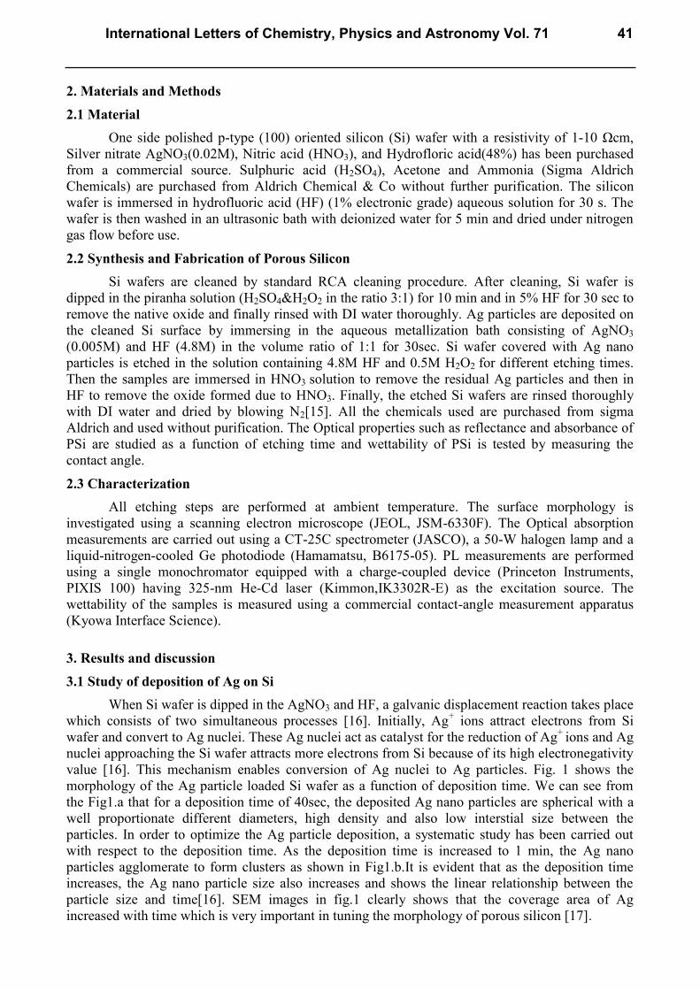
When Si wafer is dipped in the AgNO3 and HF, a galvanic displacement reaction takes place
which consists of two simultaneous processes [16]. Initially, Ag+ ions attract electrons from Si
wafer and convert to Ag nuclei. These Ag nuclei act as catalyst for the reduction of Ag+
ions and Ag
nuclei approaching the Si wafer attracts more electrons from Si because of its high electronegativity
value [16]. This mechanism enables conversion of Ag nuclei to Ag particles. Fig. 1 shows the
morphology of the Ag particle loaded Si wafer as a function of deposition time. We can see from
the Fig1.a that for a deposition time of 40sec, the deposited Ag nano particles are spherical with a
well proportionate different diameters, high density and also low interstial size between the
particles. In order to optimize the Ag particle deposition, a systematic study has been carried out
with respect to the deposition time. As the deposition time is increased to 1 min, the Ag nano
particles agglomerate to form clusters as shown in Fig1.b.It is evident that as the deposition time
increases, the Ag nano particle size also increases and shows the linear relationship between the
particle size and time[16]. SEM images in fig.1 clearly shows that the coverage area of Ag
increased with time which is very important in tuning the morphology of porous silicon [17].
International Letters of Chemistry, Physics and Astronomy Vol. 71 41
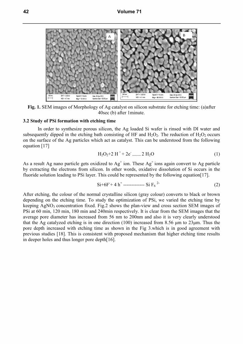
Fig. 1. SEM images of Morphology of Ag catalyst on silicon substrate for etching time: (a)after
40sec (b) after 1minute.
3.2 Study of PSi formation with etching time
In order to synthesize porous silicon, the Ag loaded Si wafer is rinsed with DI water and
subsequently dipped in the etching bath consisting of HF and H2O2. The reduction of H2O2 occurs
on the surface of the Ag particles which act as catalyst. This can be understood from the following
equation [17]
H2O2+2 H +
+ 2e- -------- 2 H2O (1)
As a result Ag nano particle gets oxidized to Ag+ ion. These Ag
+ ions again convert to Ag particle
by extracting the electrons from silicon. In other words, oxidative dissolution of Si occurs in the
fluoride solution leading to PSi layer. This could be represented by the following equation[17].
Si+6F-+ 4 h
+ ------------- Si F6
2- (2)
After etching, the colour of the normal crystalline silicon (gray colour) converts to black or brown
depending on the etching time. To study the optimization of PSi, we varied the etching time by
keeping AgNO3 concentration fixed. Fig.2 shows the plan-view and cross section SEM images of
PSi at 60 min, 120 min, 180 min and 240min respectively. It is clear from the SEM images that the
average pore diameter has increased from 56 nm to 200nm and also it is very clearly understood
that the Ag catalyzed etching is in one direction (100) increased from 8.56 μm to 23μm. Thus the
pore depth increased with etching time as shown in the Fig 3.which is in good agreement with
previous studies [18]. This is consistent with proposed mechanism that higher etching time results
in deeper holes and thus longer pore depth[16].
42 Volume 71

Fig. 2. SEM images of Porous Silicon at different etching times: a) 60 min etching b) 120 min
c) 180min d) 240 min (insets show the cross section images).
Fig. 3.Variation of Etch depth with Etching time.
3.3 Optical studies
3.3.1 Reflectance behavior
Fig.4 shows the reflectance spectra of porous silicon in the wavelength of range 300nm-
800nm. It is observed that the PSi shows lower reflectance compared to bare silicon. The maximum
reduction in light reflectance occurs with in the range of 300nm to 600nm and later it showed slight
increase in the reflectance. It is clear from the Fig.4 that the average reflectance of PSi is 40% less
than reflectance of unetched Si and the increase at higher wavelengths is probably due to the
random distribution of the pores and increased roughness. The overall attenuaton in the optical
International Letters of Chemistry, Physics and Astronomy Vol. 71 43
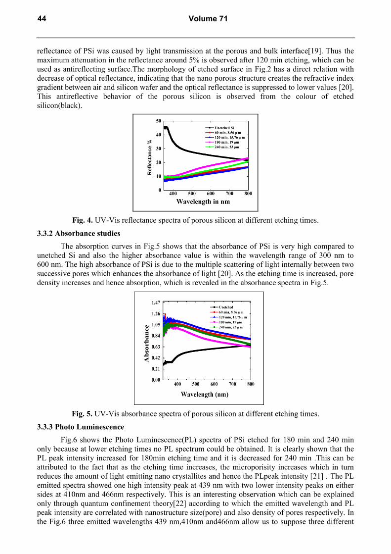
reflectance of PSi was caused by light transmission at the porous and bulk interface[19]. Thus the
maximum attenuation in the reflectance around 5% is observed after 120 min etching, which can be
used as antireflecting surface.The morphology of etched surface in Fig.2 has a direct relation with
decrease of optical reflectance, indicating that the nano porous structure creates the refractive index
gradient between air and silicon wafer and the optical reflectance is suppressed to lower values [20].
This antireflective behavior of the porous silicon is observed from the colour of etched
silicon(black).
Fig. 4. UV-Vis reflectance spectra of porous silicon at different etching times.
3.3.2 Absorbance studies
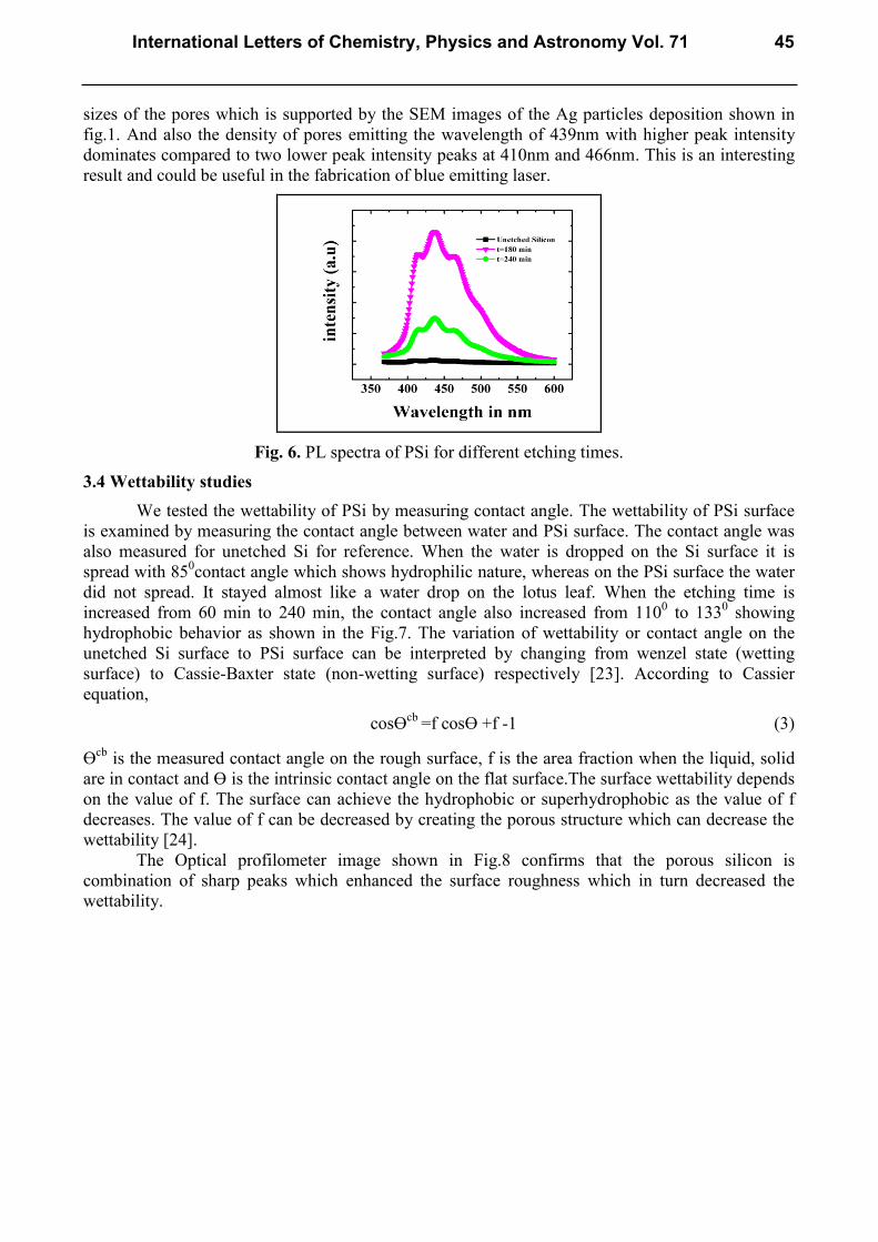
The absorption curves in Fig.5 shows that the absorbance of PSi is very high compared to
unetched Si and also the higher absorbance value is within the wavelength range of 300 nm to
600 nm. The high absorbance of PSi is due to the multiple scattering of light internally between two
successive pores which enhances the absorbance of light [20]. As the etching time is increased, pore
density increases and hence absorption, which is revealed in the absorbance spectra in Fig.5.
Fig. 5. UV-Vis absorbance spectra of porous silicon at different etching times.
3.3.3 Photo Luminescence
Fig.6 shows the Photo Luminescence(PL) spectra of PSi etched for 180 min and 240 min
only because at lower etching times no PL spectrum could be obtained. It is clearly shown that the
PL peak intensity increased for 180min etching time and it is decreased for 240 min .This can be
attributed to the fact that as the etching time increases, the microporisity increases which in turn
reduces the amount of light emitting nano crystallites and hence the PLpeak intensity [21] . The PL
emitted spectra showed one high intensity peak at 439 nm with two lower intensity peaks on either
sides at 410nm and 466nm respectively. This is an interesting observation which can be explained
only through quantum confinement theory[22] according to which the emitted wavelength and PL
peak intensity are correlated with nanostructure size(pore) and also density of pores respectively. In
the Fig.6 three emitted wavelengths 439 nm,410nm and466nm allow us to suppose three different
44 Volume 71
sizes of the pores which is supported by the SEM images of the Ag particles deposition shown in
fig.1. And also the density of pores emitting the wavelength of 439nm with higher peak intensity
dominates compared to two lower peak intensity peaks at 410nm and 466nm. This is an interesting
result and could be useful in the fabrication of blue emitting laser.
Fig. 6. PL spectra of PSi for different etching times.
3.4 Wettability studies
We tested the wettability of PSi by measuring contact angle. The wettability of PSi surface
is examined by measuring the contact angle between water and PSi surface. The contact angle was
also measured for unetched Si for reference. When the water is dropped on the Si surface it is
spread with 850contact angle which shows hydrophilic nature, whereas on the PSi surface the water
did not spread. It stayed almost like a water drop on the lotus leaf. When the etching time is
increased from 60 min to 240 min, the contact angle also increased from 1100 to 133
0 showing
hydrophobic behavior as shown in the Fig.7. The variation of wettability or contact angle on the
unetched Si surface to PSi surface can be interpreted by changing from wenzel state (wetting
surface) to Cassie-Baxter state (non-wetting surface) respectively [23]. According to Cassier
equation,
cosӨcb
=f cosӨ +f -1 (3)
Өcb
is the measured contact angle on the rough surface, f is the area fraction when the liquid, solid
are in contact and Ө is the intrinsic contact angle on the flat surface.The surface wettability depends
on the value of f. The surface can achieve the hydrophobic or superhydrophobic as the value of f
decreases. The value of f can be decreased by creating the porous structure which can decrease the
wettability [24].
The Optical profilometer image shown in Fig.8 confirms that the porous silicon is
combination of sharp peaks which enhanced the surface roughness which in turn decreased the
wettability.
International Letters of Chemistry, Physics and Astronomy Vol. 71 45
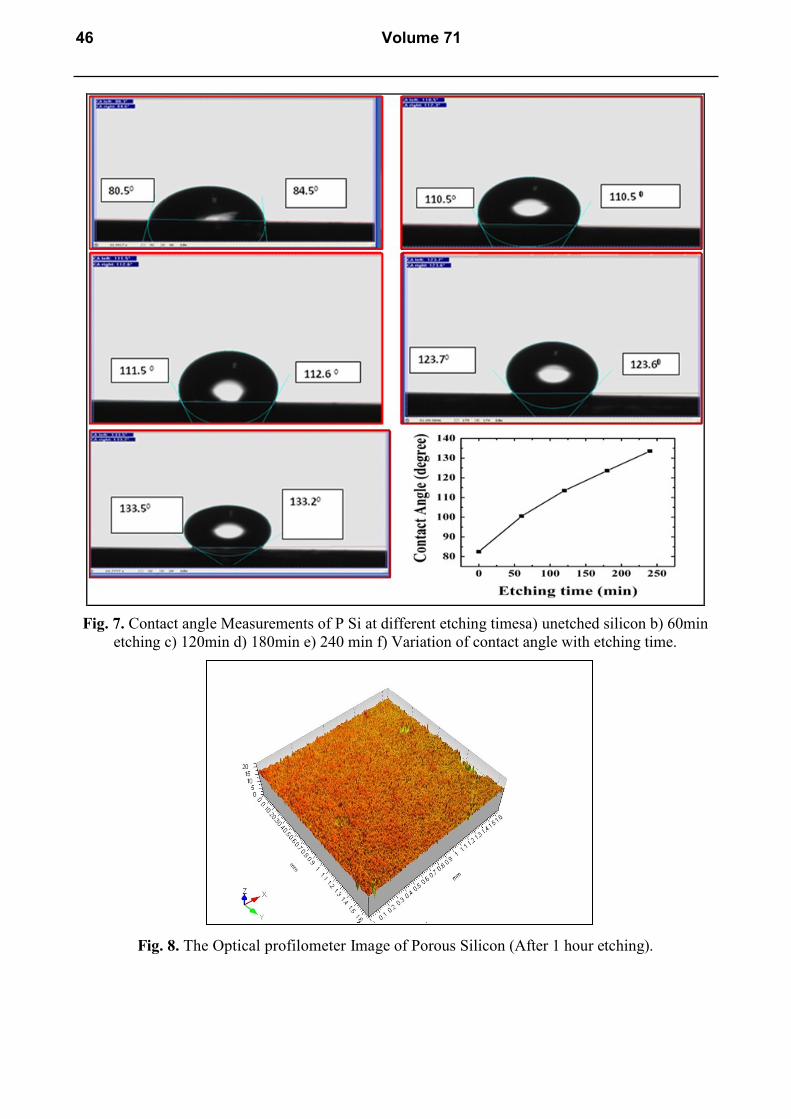
Fig. 7. Contact angle Measurements of P Si at different etching timesa) unetched silicon b) 60min
etching c) 120min d) 180min e) 240 min f) Variation of contact angle with etching time.
Fig. 8. The Optical profilometer Image of Porous Silicon (After 1 hour etching).
46 Volume 71

4. Conclusions
This study clearly demonstrated the fabrication of PSi by Ag assisted chemical etching.The
deposition of Ag nano particle size on silicon is controlled by deposition time .With the obtained
Ag deposited system, fabrication of PSi, as a function of etching time is studied in detail and
concluded that the pore depth has been increased with etching time.PSi optical and wettability
properties are studied as a function of etching time. The optical reflectance of Porous Silicon is
totally supressed almost to 10% which is very effective for enhancement of optical absorption and
in the preparation of antireflecting coatings. It is observed that the PL produced by porous silicon is
in the blue wavelength region.The static contact angle measurements of PSi with etching time
shows that an increase in the etching time results in increase of contact angle which is effective
result in achiving superhydrophobicity and self cleaning property with out any external surface
modification.Thus PSi fabricated by Ag assisted chemical etching showed low reflectance which
offers significant advantage for the high efficiency solar cells with self cleaning properties. The
superhydrophobic characteristics of porous silicon demonstrate that this material could be used as a
self cleaning surface.
Acknowledgement
The authors thank UGC, Government of India, for funding the project. Thanks also due to
their colleagues for help during this work at I.I.Sc.Bangalore.
References
[1] L.T. Canham, Silicon quantum wire array fabrication by electrochemical and chemical
dissolution of wafers, Appl. Phys. Lett. 57 (1990) 1046-1048.
[2] A. G. Cullis, L.T.Canham, P. D. J. Calcott, The structural and luminescence properties of
porous silicon, J. Appl. Phys. 82 (1997) 909 – 965.
[3] L.Brus, Luminescence of Silicon Materials: Chains, Sheets, Nanocrystals, Nanowires,
Microcrystals, and Porous Silicon, J.Phys. Chem. 98 (1994) 3575 – 3581.
[4] M. J. Sailor, E. J. Lee, Surface chemistry of luminescent silicon nanocrystallites, Adv. Mater.
9 (1997) 783 – 793.
[5] L.T. Canham, Bioactive silicon structure fabrication through nanoetching techniques, Adv.
Mater. 7 (1995) 1033-1037.
[6] V.S.Y. Lin et al., A porous silicon-based optical interferometric biosensor, Science. 278
(1997) 840-843.
[7] S.E. Letant, M. J. Sailor, Detection of HF gas with a porous silicon interferometer, Adv.
Mater. 12 (2000) 355-359.
[8] Y. Xiao et al., Controlled exfoliation of a heavily n-doped porous silicon double layer
electrochemically etched for layer-transfer photovoltaics, Electrochim Acta. 74 (2012) 93-97.
[9] K.W. Kolasinski, J.W. Gogola, Rational design of etchants for electroless porous silicon
formation, ECS Transactions. 33 (2011) 23-28.
[10] X. Li, P.W. Bohn, Metal-assisted chemical etching in HF/H2O2 produces porous silicon, Appl
.Phys .Lett. 77 (2000) 2572-2574.
[11] S. Yae et al., Formation of porous silicon by metal particle enhanced chemical etching in HF
solution and its application for efficient solar cells, Electrochem. Commun. 5 (2003) 632-636.
International Letters of Chemistry, Physics and Astronomy Vol. 71 47

[12] S. Bastide et al., Chemical etching of Si by Ag nanocatalysts in HF-H2O2: application to
multicrystalline Si solar cell texturisation, Phys Status Solidi C. 6 (2009) 1536-1540.
[13] Zhipeng Huang et al., Oxidation rate effect on the direction of metal-assisted chemical and
electrochemical etching of silicon, J. Phys. Chem. C.114 (2010) 10683-10690.
[14] Baris Ozdemir et al., Effect of electroless etching parameters on the growth and reflection
properties of silicon nanowires, Nanotechnology. 22 (2011) 155606.
[15] A. Najar et al., Effect of hydrofluoric acid concentration on the evolution of
photoluminescence characteristics in porous silicon nanowires prepared by Ag-assisted
electroless etching method, J. Appl. Phys. 112 (2012) 033502.
[16] S. Gielis et al., Silver-Assisted Etching of Silicon Nanowires, ECS Transactions. 33 (2011)
49-58.
[17] K. Tsujino, M. Matsumura, Morphology of nanoholes formed in silicon by wet etching in
solutions containing HF and H2O2 at different concentrations using silver nanoparticles as
catalysts, Electrochim. Acta. 53 (2007) 28-34.
[18] C. Chartier, S. Bastide, C. Levy-Clement, Metal assisted chemical etching of silicon in HF-
H2O2, Electrochim. Acta. 53 (2008) 5509-5516.
[19] A. Ramizy, Z. Hassan, K. Omar, Porous silicon nanowires fabricated by electrochemical and
laser-induced etching, J.Mater. Sci. Mater. Electron. 22 (2011) 717-723.
[20] Jin-Young Jung et al., A strong antireflective solar cell prepared by tapering silicon
nanowires, Opt. express. 18 (2010) A286-A292.
[21] M. Lipinskia et al., APorous Silicon Formation by Metal-Assisted Chemical Etching, Acta
Phys. Pol. 116 (2009) S117-S119.
[22] G. Ledoux et al., Photoluminescence properties of silicon nanocrystals as a function of their
size Phys. Rev. B 62 (2000) 15942 – 15951.
[23] A.B.D. Cassie, S. Baxter, Wettability of porous surfaces, Trans Faraday Soc. 40 (1944) 546-
551.
[24] Dianpeng Qi et al., Simple Approach to Wafer-Scale Self-Cleaning Antireflective Silicon
Surfaces, Langmuir. 25 (2009) 7769-7777.
48 Volume 71
Recommended


![Enhancement the electrical properties of porous silicon ... No. 3 2018 JULY/Vol_11... · Volume 11, No. 3, July 2018 [241-248] Enhancing the Electrical Properties of Porous Silicon](https://img.pdfslide.us/doc/110x75/5e130259c9499d69e11d0b35/enhancement-the-electrical-properties-of-porous-silicon-no-3-2018-julyvol11.jpg)