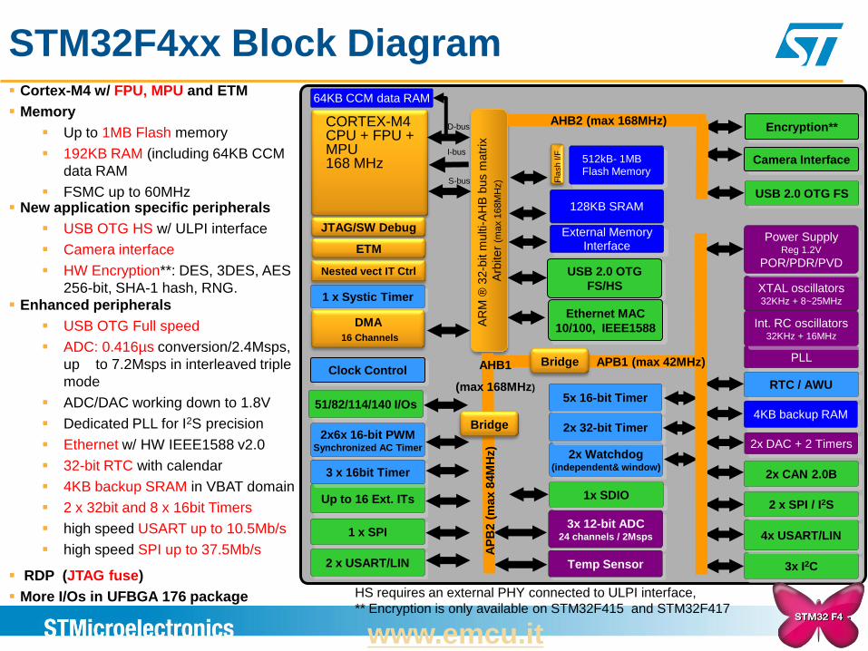
51/82/114/140 I/Os
USB 2.0 OTG
FS/HS
Encryption**
Camera Interface
3x 12-bit ADC 24 channels / 2Msps
3x I2C
Up to 16 Ext. ITs
Temp Sensor
2x6x 16-bit PWM Synchronized AC Timer
2x Watchdog (independent& window)
5x 16-bit Timer
XTAL oscillators 32KHz + 8~25MHz
Power Supply Reg 1.2V
POR/PDR/PVD
2x DAC + 2 Timers
2 x USART/LIN
1 x SPI
1 x Systic Timer
PLL Clock Control
RTC / AWU
4KB backup RAM
Ethernet MAC
10/100, IEEE1588
USB 2.0 OTG FS
4x USART/LIN
1x SDIO
Int. RC oscillators 32KHz + 16MHz
3 x 16bit Timer
2x 32-bit Timer
2x CAN 2.0B
2 x SPI / I2S
HS requires an external PHY connected to ULPI interface,
** Encryption is only available on STM32F415 and STM32F417 1
STM32F4xx Block Diagram Cortex-M4 w/ FPU, MPU and ETM
Memory
Up to 1MB Flash memory
192KB RAM (including 64KB CCM
data RAM
FSMC up to 60MHz New application specific peripherals
USB OTG HS w/ ULPI interface
Camera interface
HW Encryption**: DES, 3DES, AES
256-bit, SHA-1 hash, RNG.
Enhanced peripherals
USB OTG Full speed
ADC: 0.416µs conversion/2.4Msps,
up to 7.2Msps in interleaved triple
mode
ADC/DAC working down to 1.8V
Dedicated PLL for I2S precision
Ethernet w/ HW IEEE1588 v2.0
32-bit RTC with calendar
4KB backup SRAM in VBAT domain
2 x 32bit and 8 x 16bit Timers
high speed USART up to 10.5Mb/s
high speed SPI up to 37.5Mb/s
RDP (JTAG fuse)
More I/Os in UFBGA 176 package
AR
M ®
32-b
it m
ulti-
AH
B b
us m
atr
ix
Arb
iter
(max 1
68M
Hz) F
lash I/F
CORTEX-M4 CPU + FPU + MPU 168 MHz
128KB SRAM
JTAG/SW Debug
DMA
16 Channels
Nested vect IT Ctrl
Bridge
Bridge APB1 (max 42MHz)
ETM
512kB- 1MB Flash Memory
External Memory Interface
AHB1
(max 168MHz)
AHB2 (max 168MHz)
AP
B2 (
ma
x 8
4M
Hz)
64KB CCM data RAM
D-bus
I-bus
S-bus
www.emcu.it
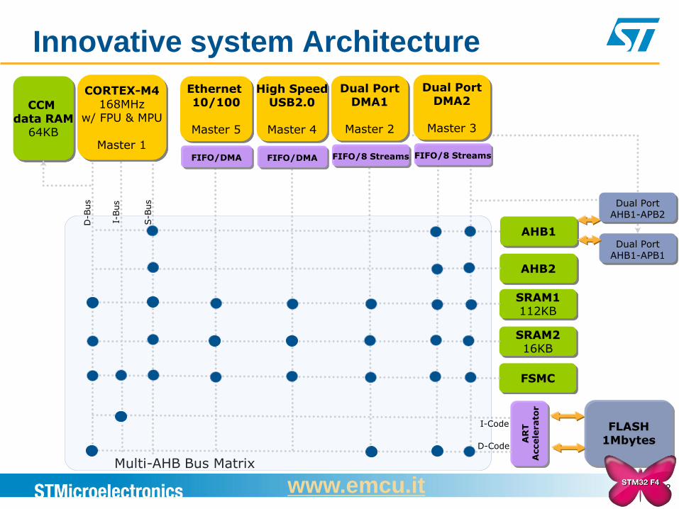
Innovative system Architecture
SRAM1 112KB
SRAM2 16KB
FSMC
AHB2
Multi-AHB Bus Matrix
AR
T
Accele
rato
r
CORTEX-M4
168MHz w/ FPU & MPU
Master 1
D-B
us
S-B
us
I-Code
D-Code
Dual Port
DMA2
Master 3
FIFO/8 Streams
AHB1
Dual Port AHB1-APB1
Dual Port
AHB1-APB2
FLASH 1Mbytes
Dual Port
DMA1
Master 2
FIFO/8 Streams
CCM
data RAM 64KB
2
High Speed
USB2.0
Master 4
FIFO/DMA
Ethernet 10/100
Master 5
FIFO/DMA
I-Bus
www.emcu.it
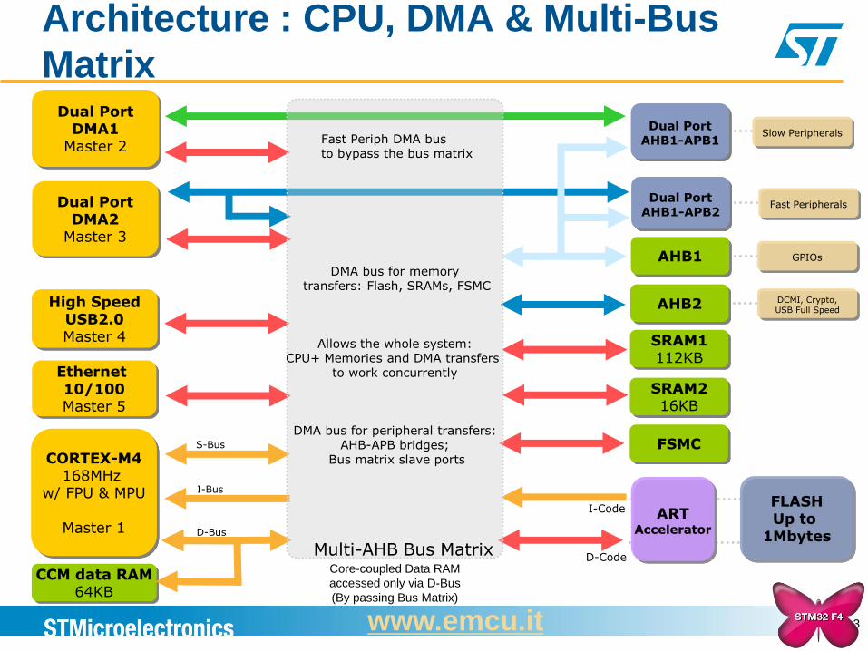
Architecture : CPU, DMA & Multi-Bus
Matrix
SRAM1 112KB
SRAM2 16KB
FSMC
AHB2
ART Accelerator
CORTEX-M4
168MHz w/ FPU & MPU
Master 1
High Speed
USB2.0 Master 4
Ethernet 10/100 Master 5
I-Code
D-Code
Dual Port
DMA1 Master 2
AHB1
Dual Port
AHB1-APB2
FLASH Up to
1Mbytes
Dual Port
DMA2 Master 3
Fast Peripherals
GPIOs
Dual Port
AHB1-APB1
Slow Peripherals
DCMI, Crypto, USB Full Speed
DMA bus for memory transfers: Flash, SRAMs, FSMC
Allows the whole system: CPU+ Memories and DMA transfers
to work concurrently
DMA bus for peripheral transfers: AHB-APB bridges;
Bus matrix slave ports
Fast Periph DMA bus to bypass the bus matrix
Multi-AHB Bus Matrix CCM data RAM
64KB
I-Bus
D-Bus
S-Bus
Core-coupled Data RAM
accessed only via D-Bus
(By passing Bus Matrix)
3 www.emcu.it
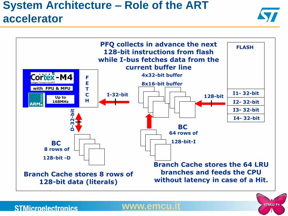
System Architecture – Role of the ART
accelerator
FLASH
I1- 32-bit
I2- 32-bit
I3- 32-bit
I4- 32-bit
I-32-bit 128-bit
Branch Cache stores the 64 LRU branches and feeds the CPU
without latency in case of a Hit.
4x32-bit buffer
8x16-bit buffer
8 rows of
128-bit -D
BC
Branch Cache stores 8 rows of 128-bit data (literals)
D-3
2-b
it
64 rows of
128-bit-I
BC
FETCH
-M4 with FPU & MPU
Up to 168MHz
PFQ collects in advance the next 128-bit instructions from flash
while I-bus fetches data from the current buffer line
www.emcu.it
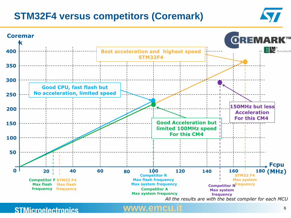
STM32F4 versus competitors (Coremark)
Fcpu (MHz)
STM32 F4 Max system frequency
Coremark
100
200
300
250
150
50
40 20 80 140 60 100 120 160
350
Competitor R Max flash frequency
Max system frequency Competitor F
Max flash frequency
STM32 F4 Max flash frequency Competitor A
Max system frequency
0
Competitor N Max system frequency
Good Acceleration but limited 100MHz speed
For this CM4
Good CPU, fast flash but No acceleration, limited speed
All the results are with the best compiler for each MCU
150MHz but less Acceleration For this CM4
400 Best acceleration and highest speed STM32F4
180
6 www.emcu.it
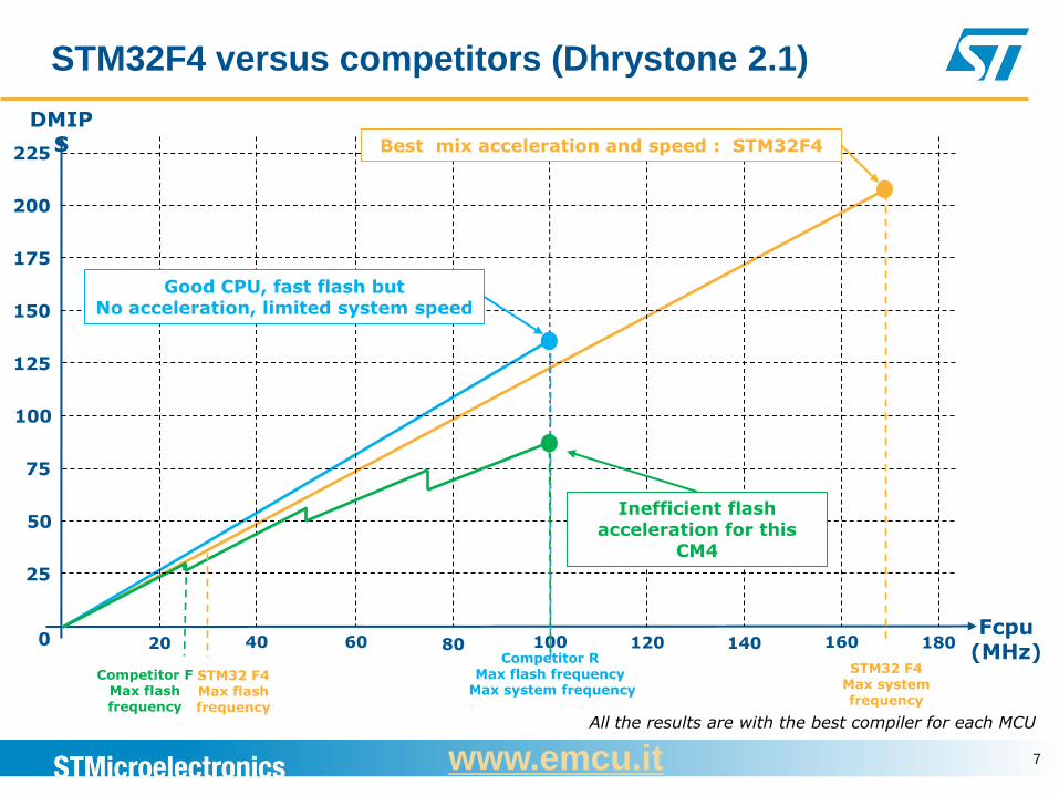
STM32F4 versus competitors (Dhrystone 2.1)
Fcpu (MHz)
STM32 F4 Max system frequency
DMIPS
50
100
150
125
75
25
40 20 80 140 60 100 120 160
175
200
Competitor R Max flash frequency
Max system frequency Competitor F
Max flash frequency
STM32 F4 Max flash frequency
0
Good CPU, fast flash but No acceleration, limited system speed
Inefficient flash acceleration for this
CM4
All the results are with the best compiler for each MCU
180
225 Best mix acceleration and speed : STM32F4
7 www.emcu.it
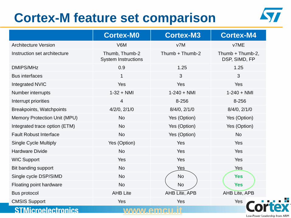
Cortex-M feature set comparison
9
Cortex-M0 Cortex-M3 Cortex-M4
Architecture Version V6M v7M v7ME
Instruction set architecture Thumb, Thumb-2
System Instructions
Thumb + Thumb-2 Thumb + Thumb-2,
DSP, SIMD, FP
DMIPS/MHz 0.9 1.25 1.25
Bus interfaces 1 3 3
Integrated NVIC Yes Yes Yes
Number interrupts 1-32 + NMI 1-240 + NMI 1-240 + NMI
Interrupt priorities 4 8-256 8-256
Breakpoints, Watchpoints 4/2/0, 2/1/0 8/4/0, 2/1/0 8/4/0, 2/1/0
Memory Protection Unit (MPU) No Yes (Option) Yes (Option)
Integrated trace option (ETM) No Yes (Option) Yes (Option)
Fault Robust Interface No Yes (Option) No
Single Cycle Multiply Yes (Option) Yes Yes
Hardware Divide No Yes Yes
WIC Support Yes Yes Yes
Bit banding support No Yes Yes
Single cycle DSP/SIMD No No Yes
Floating point hardware No No Yes
Bus protocol AHB Lite AHB Lite, APB AHB Lite, APB
CMSIS Support Yes Yes Yes
www.emcu.it
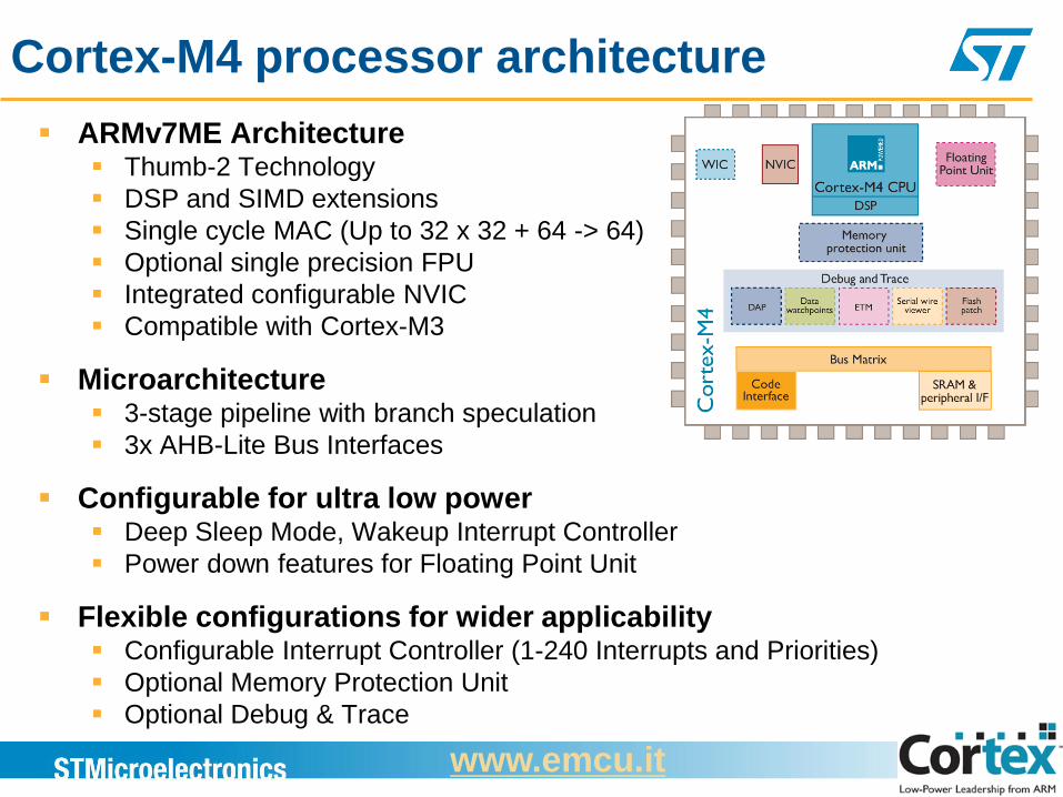
Cortex-M4 processor architecture
ARMv7ME Architecture Thumb-2 Technology
DSP and SIMD extensions
Single cycle MAC (Up to 32 x 32 + 64 -> 64)
Optional single precision FPU
Integrated configurable NVIC
Compatible with Cortex-M3
Microarchitecture 3-stage pipeline with branch speculation
3x AHB-Lite Bus Interfaces
Configurable for ultra low power Deep Sleep Mode, Wakeup Interrupt Controller
Power down features for Floating Point Unit
Flexible configurations for wider applicability Configurable Interrupt Controller (1-240 Interrupts and Priorities)
Optional Memory Protection Unit
Optional Debug & Trace
11 www.emcu.it
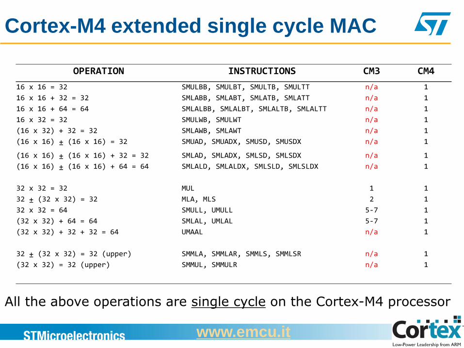
Cortex-M4 extended single cycle MAC
OPERATION INSTRUCTIONS CM3 CM4
16 x 16 = 32 SMULBB, SMULBT, SMULTB, SMULTT n/a 1
16 x 16 + 32 = 32 SMLABB, SMLABT, SMLATB, SMLATT n/a 1
16 x 16 + 64 = 64 SMLALBB, SMLALBT, SMLALTB, SMLALTT n/a 1
16 x 32 = 32 SMULWB, SMULWT n/a 1
(16 x 32) + 32 = 32 SMLAWB, SMLAWT n/a 1
(16 x 16) ± (16 x 16) = 32 SMUAD, SMUADX, SMUSD, SMUSDX n/a 1
(16 x 16) ± (16 x 16) + 32 = 32 SMLAD, SMLADX, SMLSD, SMLSDX n/a 1
(16 x 16) ± (16 x 16) + 64 = 64 SMLALD, SMLALDX, SMLSLD, SMLSLDX n/a 1
32 x 32 = 32 MUL 1 1
32 ± (32 x 32) = 32 MLA, MLS 2 1
32 x 32 = 64 SMULL, UMULL 5-7 1
(32 x 32) + 64 = 64 SMLAL, UMLAL 5-7 1
(32 x 32) + 32 + 32 = 64 UMAAL n/a 1
32 ± (32 x 32) = 32 (upper) SMMLA, SMMLAR, SMMLS, SMMLSR n/a 1
(32 x 32) = 32 (upper) SMMUL, SMMULR n/a 1
All the above operations are single cycle on the Cortex-M4 processor
www.emcu.it
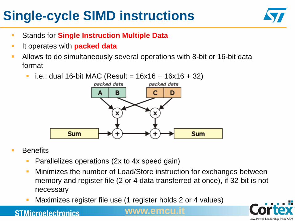
Single-cycle SIMD instructions
Stands for Single Instruction Multiple Data
It operates with packed data
Allows to do simultaneously several operations with 8-bit or 16-bit data
format
i.e.: dual 16-bit MAC (Result = 16x16 + 16x16 + 32)
Benefits
Parallelizes operations (2x to 4x speed gain)
Minimizes the number of Load/Store instruction for exchanges between
memory and register file (2 or 4 data transferred at once), if 32-bit is not
necessary
Maximizes register file use (1 register holds 2 or 4 values)
www.emcu.it
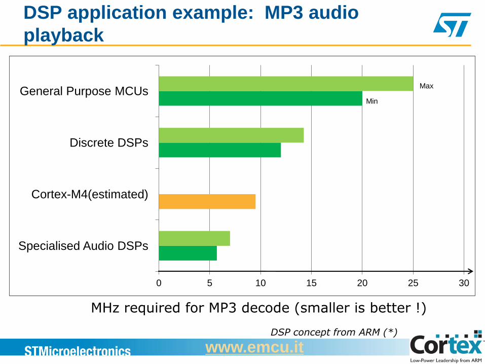
DSP application example: MP3 audio
playback
0 5 10 15 20 25 30
Specialised Audio DSPs
Cortex-M4(estimated)
Discrete DSPs
General Purpose MCUs Max
Min
MHz required for MP3 decode (smaller is better !)
14
DSP concept from ARM (*)
www.emcu.it
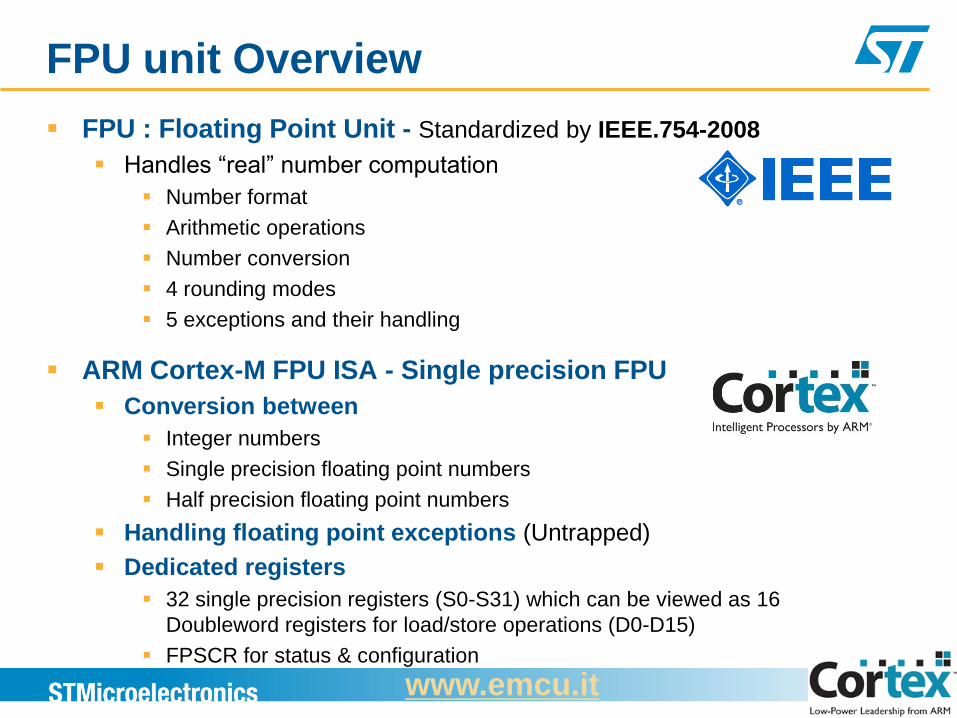
FPU unit Overview
FPU : Floating Point Unit - Standardized by IEEE.754-2008
Handles “real” number computation
Number format
Arithmetic operations
Number conversion
4 rounding modes
5 exceptions and their handling
ARM Cortex-M FPU ISA - Single precision FPU
Conversion between
Integer numbers
Single precision floating point numbers
Half precision floating point numbers
Handling floating point exceptions (Untrapped)
Dedicated registers
32 single precision registers (S0-S31) which can be viewed as 16
Doubleword registers for load/store operations (D0-D15)
FPSCR for status & configuration
www.emcu.it
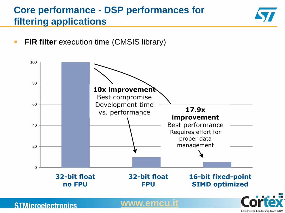
Core performance - DSP performances for
filtering applications
FIR filter execution time (CMSIS library)
0
20
40
60
80
100
32-bit float no FPU
32-bit float FPU
16-bit fixed-point SIMD optimized
10x improvement Best compromise Development time vs. performance 17.9x
improvement Best performance Requires effort for
proper data management
16 www.emcu.it
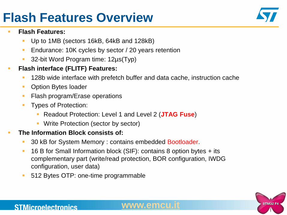
Flash Features Overview Flash Features:
Up to 1MB (sectors 16kB, 64kB and 128kB)
Endurance: 10K cycles by sector / 20 years retention
32-bit Word Program time: 12µs(Typ)
Flash interface (FLITF) Features:
128b wide interface with prefetch buffer and data cache, instruction cache
Option Bytes loader
Flash program/Erase operations
Types of Protection:
Readout Protection: Level 1 and Level 2 (JTAG Fuse)
Write Protection (sector by sector)
The Information Block consists of:
30 kB for System Memory : contains embedded Bootloader.
16 B for Small Information block (SIF): contains 8 option bytes + its
complementary part (write/read protection, BOR configuration, IWDG
configuration, user data)
512 Bytes OTP: one-time programmable
www.emcu.it
DMA Features
Dual AHB master bus architecture, one dedicated to memory accesses and one dedicated to peripheral accesses.
8 streams for each DMA controller, up to 8 channels (requests) per stream (2 DMA controllers in STM32F4xx family). Channel selection for each stream is software-configurable.
4x32-Bits FIFO memory for each Stream (FIFO mode can be enabled or disabled).
Independent source and destination transfer width (byte, half-word, word): when the source and destination data widths are different, the DMA automatically packs/unpacks data to optimize the bandwidth. (this feature is available only when FIFO mode is enabled)
Double buffer mode (double buffer mode can enabled or disabled).
Support software trigger for memory-to-memory transfers (available for the DMA2 controller streams only)
www.emcu.it
DMA Features
The number of data to be transferred can be managed either by the DMA
controller or by the peripheral
Independent Incrementing or Non-Incrementing addressing for source and
destination. Possibility to set increment offset for peripheral address.
Supports incremental burst transfers of 4, 8 or 16 beats. The size of the burst
is software-configurable, usually equal to half the FIFO size of the peripheral
Each stream supports circular buffer management.
5 event flags logically ORed together in a single interrupt request for each stream
Priorities between DMA stream requests are software-programmable
www.emcu.it
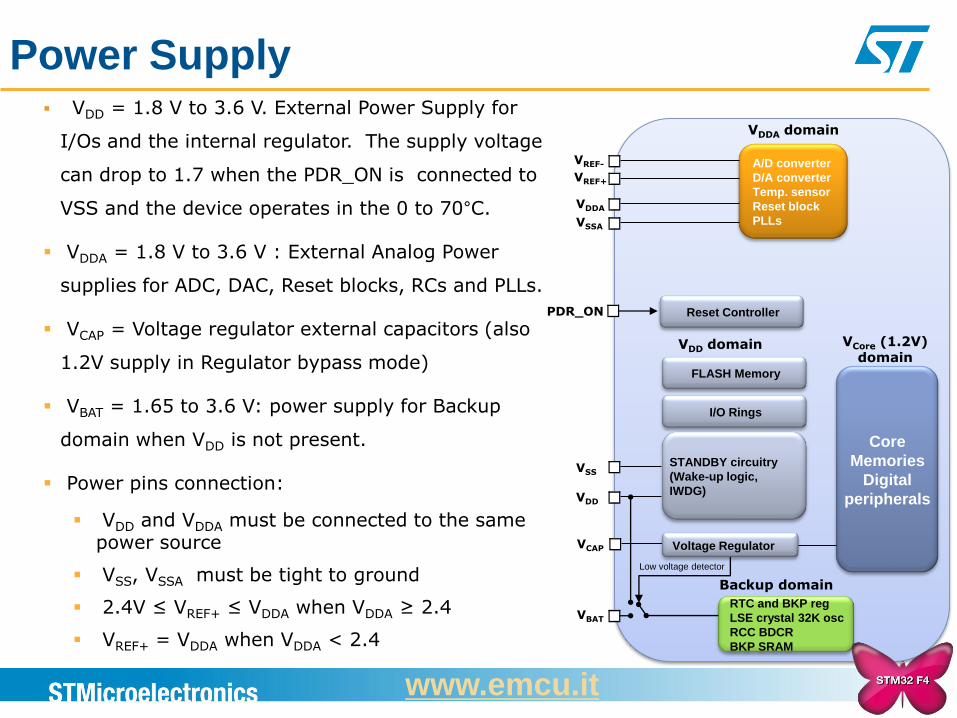
Power Supply
VSS
VBAT
VDDA
VSSA
VREF-
VREF+
A/D converter
D/A converter
Temp. sensor
Reset block
PLLs
VDDA domain
Core
Memories
Digital
peripherals
VCore (1.2V) domain
VDD domain
STANDBY circuitry
(Wake-up logic,
IWDG) VDD
VDD = 1.8 V to 3.6 V. External Power Supply for
I/Os and the internal regulator. The supply voltage
can drop to 1.7 when the PDR_ON is connected to
VSS and the device operates in the 0 to 70°C.
VDDA = 1.8 V to 3.6 V : External Analog Power
supplies for ADC, DAC, Reset blocks, RCs and PLLs.
VCAP = Voltage regulator external capacitors (also
1.2V supply in Regulator bypass mode)
VBAT = 1.65 to 3.6 V: power supply for Backup
domain when VDD is not present.
Power pins connection:
VDD and VDDA must be connected to the same power source
VSS, VSSA must be tight to ground
2.4V ≤ VREF+ ≤ VDDA when VDDA ≥ 2.4
VREF+ = VDDA when VDDA < 2.4
RTC and BKP reg
LSE crystal 32K osc
RCC BDCR
BKP SRAM
I/O Rings
FLASH Memory
Backup domain
VCAP
Low voltage detector
Reset Controller PDR_ON
Voltage Regulator
www.emcu.it
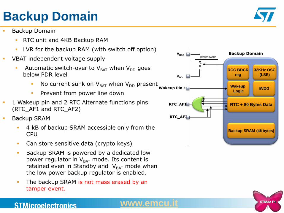
Backup Domain
RTC unit and 4KB Backup RAM
LVR for the backup RAM (with switch off option)
VBAT independent voltage supply
Automatic switch-over to VBAT when VDD goes below PDR level
No current sunk on VBAT when VDD present
Prevent from power line down
1 Wakeup pin and 2 RTC Alternate functions pins (RTC_AF1 and RTC_AF2)
Backup SRAM
4 kB of backup SRAM accessible only from the CPU
Can store sensitive data (crypto keys)
Backup SRAM is powered by a dedicated low power regulator in VBAT mode. Its content is retained even in Standby and VBAT mode when the low power backup regulator is enabled.
The backup SRAM is not mass erased by an tamper event.
Backup Domain
Backup Domain
32KHz OSC
(LSE)
RTC + 80 Bytes Data RTC_AF1
RCC BDCR
reg
Wakeup
Logic IWDG Wakeup Pin 1
RTC_AF2
Backup SRAM (4Kbytes)
VBAT
VDD
power switch
www.emcu.it
STM32F4xx Low power modes features
The STM32F4xx features 3 low power modes SLEEP (core stopped, peripherals running) ~2mA @2MHz (38mA @120MHz)
STOP (clocks stopped, RAM, registers kept) ~1mA current consumption
STANDBY (only backup domain kept, return via RESET)
VBAT mode (like in STANDBY mode).
The STM32F4xx features options to decrease the consumption during low power modes Peripherals clock stopped automatically during sleep mode (S/W)
Flash Power Down mode
LVR and Backup RAM disable option
The STM32F4xx features many sources to wakeup the system from low power modes: Wakeup pin (PA0) / NRST pin
RTC Alarm (Alarm A and Alarm B)
RTC Wakeup Timer interrupt
RTC Tamper events
RTC Time Stamp Event
IWDG Reset event
www.emcu.it
STM32F4 - clock features
Four oscillators on board HSE (High Speed External Osc) 4..26MHz (can be bypassed by and ext. Oscillator)
HSI (High Speed Internal RC): factory trimmed internal RC oscillator 16MHz +/- 1
LSI (Low Speed Internal RC): 32kHz internal RC used for IWDG, optionally RTC and AWU
LSE (Low Speed External oscillator): 32.768kHz osc (can be bypassed by an external Osc)
precise time base with very low power consumption (max 1µA).
optionally drives the RTC for Auto Wake-Up (AWU) from STOP/STANDBY mode.
Two PLLs
Main PLL (PLL) clocked by HSI or HSE used to generate the System clock (up to 168MHz),
and 48 MHz clock for USB OTG FS, SDIO and RNG. PLL input clock in the range 1-2 MHz.
PLLI2S PLL (PLLI2S) used to generate a clock to achieve HQ audio performance on the
I2S interface.
More security Clock Security System (CSS, enabled by software) to backup clock in case of HSE clock
failure (HSI feeds the system clock) – linked to Cortex NMI interrupt
Spread Spectrum Clock Generation (SSCG, enabled by software) to reduce the spectral
density of the electromagnetic interference (EMI) generated by the device
www.emcu.it
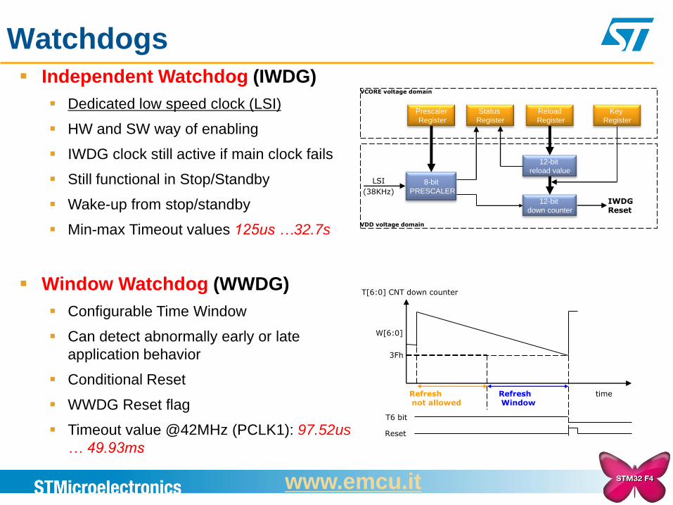
Watchdogs Independent Watchdog (IWDG)
Dedicated low speed clock (LSI)
HW and SW way of enabling
IWDG clock still active if main clock fails
Still functional in Stop/Standby
Wake-up from stop/standby
Min-max Timeout values 125us …32.7s
Window Watchdog (WWDG)
Configurable Time Window
Can detect abnormally early or late
application behavior
Conditional Reset
WWDG Reset flag
Timeout value @42MHz (PCLK1): 97.52us
… 49.93ms
8-bit
PRESCALER
LSI
(38KHz)
12-bit
reload value
12-bit
down counter
Prescaler
Register
Status
Register
Reload
Register
Key
Register
IWDG Reset
VDD voltage domain
VCORE voltage domain
Refresh not allowed
Refresh Window
T[6:0] CNT down counter
time
W[6:0]
3Fh
T6 bit
Reset
www.emcu.it
GPIO features
Up to 140 multifunction bi-directional I/O ports available on 176 pin package
Almost standard I/Os are 5V tolerant
All Standard I/Os are shared in 9 ports (GPIOA..GPIOI)
Atomic Bit Set and Bit Reset using BSRR register
GPIO connected to AHB bus: max toggling frequency = fAHB/2 = 84 MHz
Configurable Output Speed up to 100 MHz (2MHz,25MHz,50MHz,100MHz)
Locking mechanism (GPIOx_LCKR) provided to freeze the I/O configuration
Up to 140 GPIOs can be set-up as external interrupt (up to 16 lines at time) able to wake-up the MCU from low power modes
Most of the I/O pins are shared with Alternate Functions pins connected to onboard peripherals through a multiplexer that allows only one peripheral‟s alternate function to be connected to an I/O pin at a time
www.emcu.it
ADC Features (1/2)
3 ADCs : ADC1 (master), ADC2 and ADC3 (slaves)
Maximum frequency of the ADC analog clock is 36MHz.
12-bits, 10-bits, 8-bits or 6-bits configurable resolution.
ADC conversion rate with 12 bit resolution is up to:
2.4 M.sample/s in single ADC mode,
4.5 M.sample/s in dual interleaved ADC mode,
7.2 M.sample/s in triple interleaved ADC mode.
Conversion range: 0 to 3.6 V.
ADC supply requirement: VDDA = 2.4V to 3.6V at full speed and down to 1.65V
at lower speed.
Up to 24 external channels.
3 ADC1 internal channels connected to:
Temperature sensor,
Internal voltage reference : VREFINT (1.2V typ),
VBAT for internal battery monitoring.
www.emcu.it
ADC Features (2/2)
External trigger option for both regular and injected conversion.
Single and continuous conversion modes.
Scan mode for automatic conversion of channel 0 to channel „n‟.
Left or right data alignment with in-built data coherency.
Channel by channel programmable sampling time.
Discontinuous mode.
Dual/Triple mode (with ADC1 and ADC2 or all 3 ADCs).
DMA capability
Analog Watchdog on high and low thresholds.
Interrupt generation on:
End of Conversion
End of Injected conversion
Analog watchdog
Overrun
www.emcu.it
DAC Features
Two DAC converters: one output channel for each one
8-bit or 12-bit monotonic output
Left or right data alignment in 12-bit mode
Synchronized update capability
Noise-wave or Triangular-wave generation
Dual DAC channel independent or simultaneous conversions
11 dual channel modes
DMA capability for each channel
External triggers for conversion
DAC supply requirement: 1.8V to 3.6 V
Conversion range: 0 to 3.6 V
DAC outputs range: 0 ≤ DAC_OUTx ≤ VREF+ (VREF+ is available
only in 100, 144 and 176 pins package)
www.emcu.it
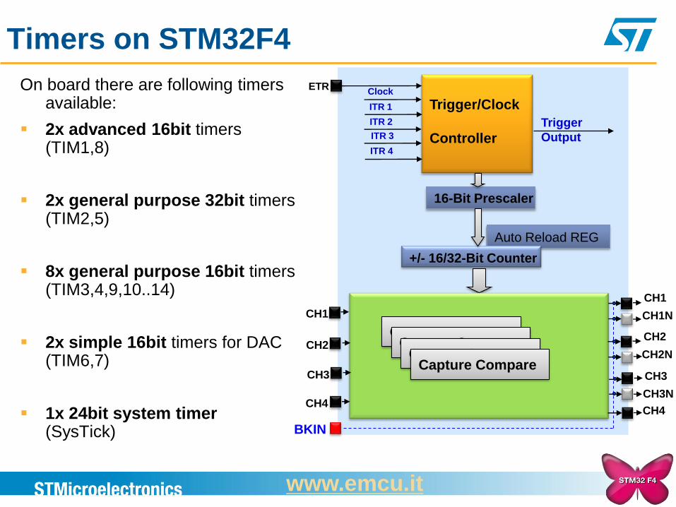
Timers on STM32F4
CH1
CH1N
CH2
CH2N
CH3
CH3N
CH4
16-Bit Prescaler
ITR 1
Trigger/Clock
Controller
Trigger
Output
Clock
Auto Reload REG
+/- 16/32-Bit Counter
Capture Compare
ITR 2
ITR 3
ITR 4
BKIN
Capture Compare Capture Compare
Capture Compare
CH1
CH2
CH3
CH4
ETR On board there are following timers available:
2x advanced 16bit timers (TIM1,8)
2x general purpose 32bit timers (TIM2,5)
8x general purpose 16bit timers (TIM3,4,9,10..14)
2x simple 16bit timers for DAC (TIM6,7)
1x 24bit system timer (SysTick)
www.emcu.it
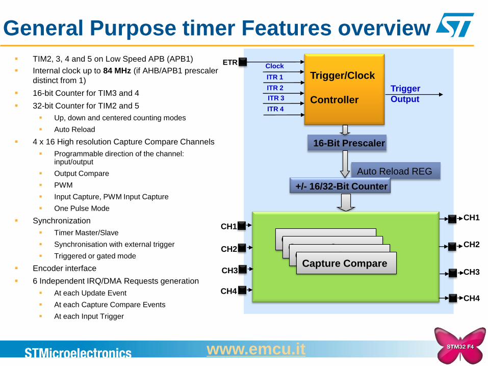
General Purpose timer Features overview
16-Bit Prescaler
ITR 1
Trigger/Clock
Controller
Trigger
Output
Clock
Auto Reload REG
+/- 16/32-Bit Counter
Capture Compare
ITR 2
ITR 3
ITR 4
Capture Compare Capture Compare
Capture Compare
CH1
CH2
CH3
CH4
ETR
CH1
CH2
CH3
CH4
TIM2, 3, 4 and 5 on Low Speed APB (APB1)
Internal clock up to 84 MHz (if AHB/APB1 prescaler
distinct from 1)
16-bit Counter for TIM3 and 4
32-bit Counter for TIM2 and 5
Up, down and centered counting modes
Auto Reload
4 x 16 High resolution Capture Compare Channels
Programmable direction of the channel: input/output
Output Compare
PWM
Input Capture, PWM Input Capture
One Pulse Mode
Synchronization
Timer Master/Slave
Synchronisation with external trigger
Triggered or gated mode
Encoder interface
6 Independent IRQ/DMA Requests generation
At each Update Event
At each Capture Compare Events
At each Input Trigger
www.emcu.it
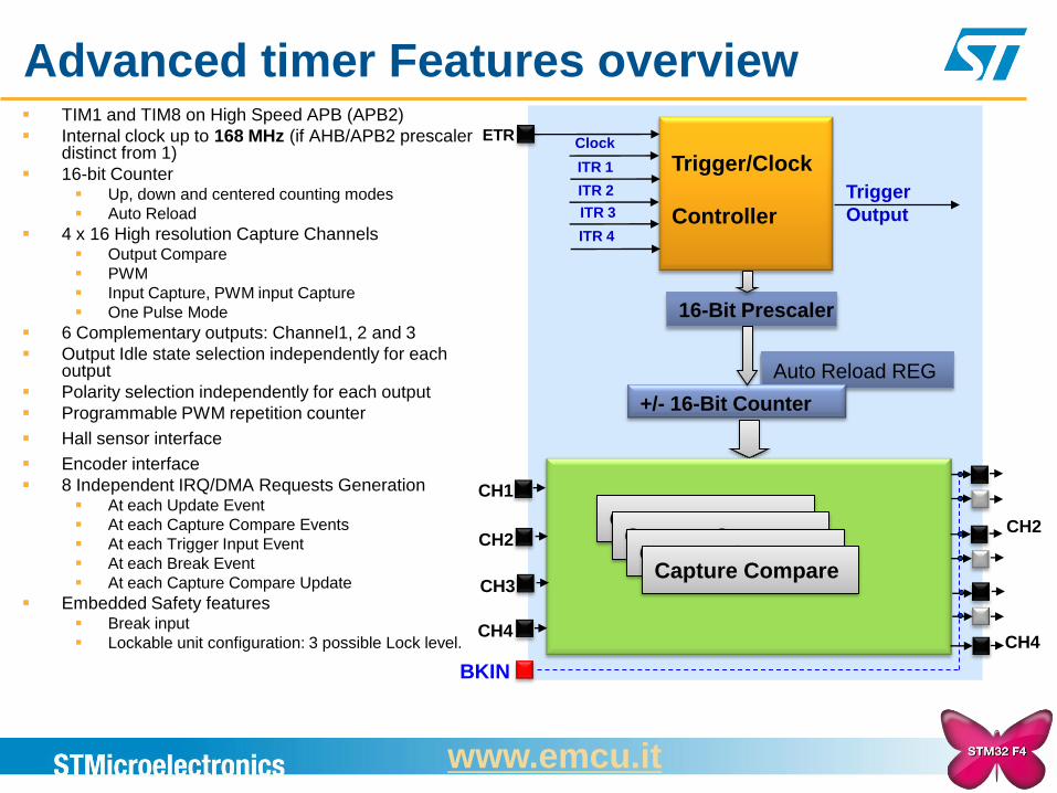
Advanced timer Features overview TIM1 and TIM8 on High Speed APB (APB2)
Internal clock up to 168 MHz (if AHB/APB2 prescaler distinct from 1)
16-bit Counter Up, down and centered counting modes
Auto Reload
4 x 16 High resolution Capture Channels Output Compare
PWM
Input Capture, PWM input Capture
One Pulse Mode
6 Complementary outputs: Channel1, 2 and 3
Output Idle state selection independently for each output
Polarity selection independently for each output
Programmable PWM repetition counter
Hall sensor interface
Encoder interface
8 Independent IRQ/DMA Requests Generation At each Update Event
At each Capture Compare Events
At each Trigger Input Event
At each Break Event
At each Capture Compare Update
Embedded Safety features Break input
Lockable unit configuration: 3 possible Lock level.
CH2
CH4
16-Bit Prescaler
ITR 1
Trigger/Clock
Controller
Trigger
Output
Clock
Auto Reload REG
+/- 16-Bit Counter
Capture Compare
ITR 2
ITR 3
ITR 4
BKIN
Capture Compare Capture Compare
Capture Compare
CH1
CH2
CH3
CH4
ETR
www.emcu.it
RTC Features
Ultra-low power battery supply current < 1uA with RTC ON.
Calendar with sub seconds, seconds, minutes, hours, week day, date, month,
and year.
Daylight saving compensation programmable by software
Two programmable alarms with interrupt function. The alarms can be triggered by
any combination of the calendar fields.
A periodic flag triggering an automatic wakeup interrupt. This flag is issued by a
16-bit auto-reload timer with programmable resolution. This timer is also called
„wakeup timer‟.
A second clock source (50 or 60Hz) can be used to update the calendar.
Maskable interrupts/events:
Alarm A, Alarm B, Wakeup interrupt, Time-stamp, Tamper detection
Digital calibration circuit (periodic counter correction) to achieve 5 ppm accuracy
Time-stamp function for event saving with sub second precision (1 event)
20 backup registers (80 bytes) which are reset when an tamper detection event
occurs.
www.emcu.it
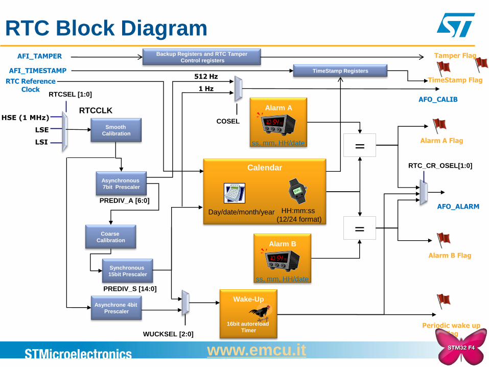
RTC Block Diagram
Asynchronous
7bit Prescaler
Synchronous
15bit Prescaler
Wake-Up
16bit autoreload
Timer
Asynchrone 4bit
Prescaler
=
Periodic wake up Flag
Alarm A Flag
AFO_ALARM
Calendar
Day/date/month/year HH:mm:ss
(12/24 format)
Alarm A
ss, mm, HH/date
WUCKSEL [2:0]
RTC_CR_OSEL[1:0]
AFO_CALIB
512 Hz
HSE (1 MHz)
RTCSEL [1:0]
LSE
LSI
RTCCLK
PREDIV_A [6:0]
PREDIV_S [14:0]
Coarse
Calibration
=
Alarm B Flag
Alarm B
ss, mm, HH/date
AFI_TAMPER
AFI_TIMESTAMP
Backup Registers and RTC Tamper
Control registers
TimeStamp Registers
TimeStamp Flag
Tamper Flag
RTC Reference Clock
Smooth
Calibration
1 Hz
COSEL
www.emcu.it
DCMI Features The Digital Camera Interface has the following main features:
8-, 10-, 12- or 14-bit parallel interface
Continuous or snapshot mode
Crop feature
Supports the following data formats:
8/10/12/14- bit progressive scan: either monochrome or raw bayer
YCbCr 4:2:2 progressive scan
RGB 565 progressive video
Compressed data: JPEG
With a 48MHz PIXCLK and 8-bit parallel input data interface it is possible to receive:
up to 15fps uncompressed data stream in SXGA resolution (1280x1024) with 16-bit per pixel
up to 30fps uncompressed data stream in VGA resolution (640x480) with 16-bit per pixel
www.emcu.it
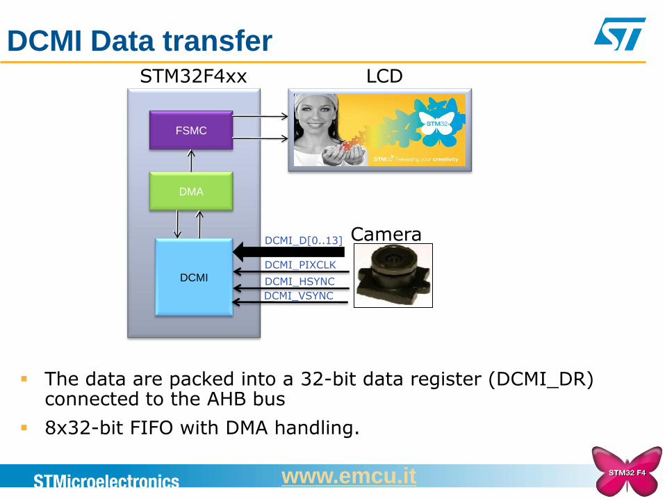
DCMI Data transfer
FSMC
DMA
DCMI
LCD STM32F4xx
DCMI_PIXCLK
DCMI_D[0..13]
DCMI_HSYNC
DCMI_VSYNC
Camera
The data are packed into a 32-bit data register (DCMI_DR) connected to the AHB bus
8x32-bit FIFO with DMA handling.
www.emcu.it
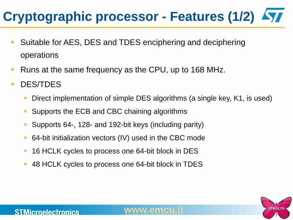
Cryptographic processor - Features (1/2)
Suitable for AES, DES and TDES enciphering and deciphering
operations
Runs at the same frequency as the CPU, up to 168 MHz.
DES/TDES
Direct implementation of simple DES algorithms (a single key, K1, is used)
Supports the ECB and CBC chaining algorithms
Supports 64-, 128- and 192-bit keys (including parity)
64-bit initialization vectors (IV) used in the CBC mode
16 HCLK cycles to process one 64-bit block in DES
48 HCLK cycles to process one 64-bit block in TDES
www.emcu.it
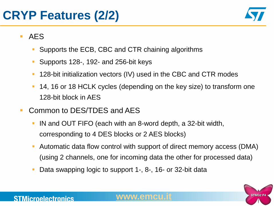
CRYP Features (2/2)
AES
Supports the ECB, CBC and CTR chaining algorithms
Supports 128-, 192- and 256-bit keys
128-bit initialization vectors (IV) used in the CBC and CTR modes
14, 16 or 18 HCLK cycles (depending on the key size) to transform one
128-bit block in AES
Common to DES/TDES and AES
IN and OUT FIFO (each with an 8-word depth, a 32-bit width,
corresponding to 4 DES blocks or 2 AES blocks)
Automatic data flow control with support of direct memory access (DMA)
(using 2 channels, one for incoming data the other for processed data)
Data swapping logic to support 1-, 8-, 16- or 32-bit data
www.emcu.it
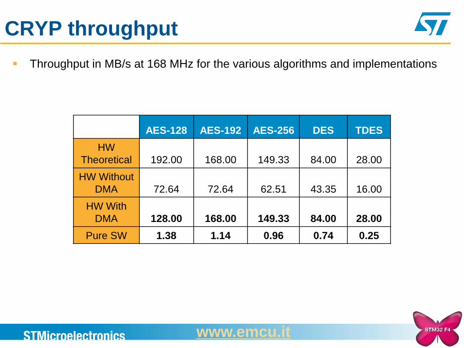
CRYP throughput
AES-128 AES-192 AES-256 DES TDES
HW
Theoretical 192.00 168.00 149.33 84.00 28.00
HW Without
DMA 72.64 72.64 62.51 43.35 16.00
HW With
DMA 128.00 168.00 149.33 84.00 28.00
Pure SW 1.38 1.14 0.96 0.74 0.25
Throughput in MB/s at 168 MHz for the various algorithms and implementations
www.emcu.it
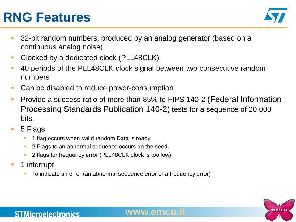
RNG Features
32-bit random numbers, produced by an analog generator (based on a
continuous analog noise)
Clocked by a dedicated clock (PLL48CLK)
40 periods of the PLL48CLK clock signal between two consecutive random
numbers
Can be disabled to reduce power-consumption
Provide a success ratio of more than 85% to FIPS 140-2 (Federal Information
Processing Standards Publication 140-2) tests for a sequence of 20 000
bits.
5 Flags 1 flag occurs when Valid random Data is ready
2 Flags to an abnormal sequence occurs on the seed.
2 flags for frequency error (PLL48CLK clock is too low).
1 interrupt To indicate an error (an abnormal sequence error or a frequency error)
www.emcu.it
HASH Features Suitable for Integrity check and data authentication applications, compliant with:
FIPS PUB 180-2 (Federal Information Processing Standards Publication 180-2)
Secure Hash Standard specifications (SHA-1)
IETF RFC 1321 (Internet Engineering Task Force Request For Comments
number 1321) specifications (MD5)
AHB slave peripheral
Fast computation of SHA-1 and MD5 :
66 HCLK clock cycles in SHA-1
50 HCLK clock cycles in MD5
5 × (32-bit) words (H0, H1, H2, H3 and H4) for output message digest, reload able
to continue interrupted message digest computation
Automatic data flow control with support for direct memory access (DMA)
32-bit data words for input data, supporting word, half-word, byte and bit bit-string
representations, with little-endian data representation only
www.emcu.it
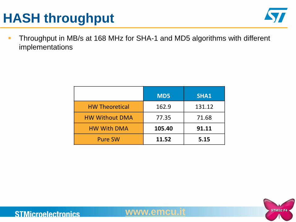
MD5 SHA1
HW Theoretical 162.9 131.12
HW Without DMA 77.35 71.68
HW With DMA 105.40 91.11
Pure SW 11.52 5.15
Throughput in MB/s at 168 MHz for SHA-1 and MD5 algorithms with different
implementations
HASH throughput
www.emcu.it
I2C Features (1/2)
Multi Master and slave capability
Controls all I²C bus specific sequencing, protocol, arbitration and timing
Standard and fast I²C mode (up to 400kHz)
7-bit and 10-bit addressing modes
Dual Addressing Capability to acknowledge 2 slave addresses
Status flags:
Transmitter/Receiver mode flag
End-of-Byte transmission flag
I2C busy flag
Configurable PEC (Packet Error Checking) Generation or Verification:
PEC value can be transmitted as last byte in Tx mode
PEC error checking for last received byte
Same as STM32F-1
www.emcu.it
I2C Features (2/2)
Error flags:
Arbitration lost condition for master mode
Acknowledgement failure after address/ data transmission
Detection of misplaced start or stop condition
Overrun/Underrun if clock stretching is disabled
2 Interrupt vectors:
1 Interrupt for successful address/ data communication
1 Interrupt for error condition
1-byte buffer with DMA capability
SMBus 2.0 Compatibility
PMBus Compatibility
www.emcu.it
USART Features (1/2) 6 USARTs: USART1 & USART6 on APB2 and USART2,3,4,5 on APB1
Fully-programmable serial interface characteristics:
Data can be 8 or 9 bits
Even, odd or no-parity bit generation and detection
0.5, 1, 1.5 or 2 stop bit generation
Oversampling by 16 (default) or by 8
Programmable baud rate generator
Integer part (12 bits)
Fractional part (4 bits)
Baud rate for standard USART (SPI mode included)
Tx/Rx baud = fck/8x(2-OVR8)xUSARTDIV Where:
Tx/Rx baud: desired baudrate
OVR8: oversampling by 8 (1 if enabled, 0 if disabled)
fck: APB frequency
USARTDIV: value to be programmed to the BRR register
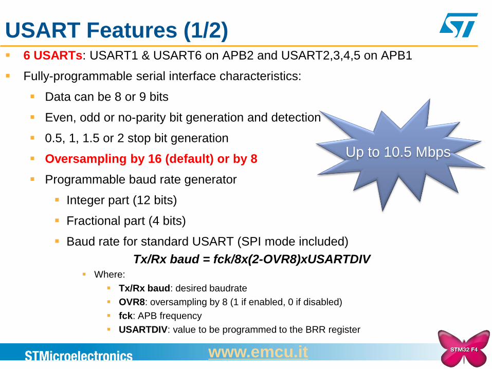
Up to 10.5 Mbps
www.emcu.it
USART Features (2/2)
Support hardware flow control (CTS and RTS)
Dedicated transmission and reception flags (TxE and RxNE) with interrupt capability
Support for DMA
Receive DMA request and Transmit DMA request
10 interrupt sources to ease software implementation
LIN Master/Slave compatible
Synchronous Mode: Master mode only
IrDA SIR Encoder Decoder
Smartcard Capability
Single wire Half Duplex Communication
Multi-Processor communication
USART can enter Mute mode
Mute mode: disable receive interrupts until next header detected
Wake up from mute mode (by idle line detection or address mark detection)
Support One Sample Bit method: allows to disable noise detection (for noise-free applications) in order to increase the receiver‟s tolerance to clock deviations.
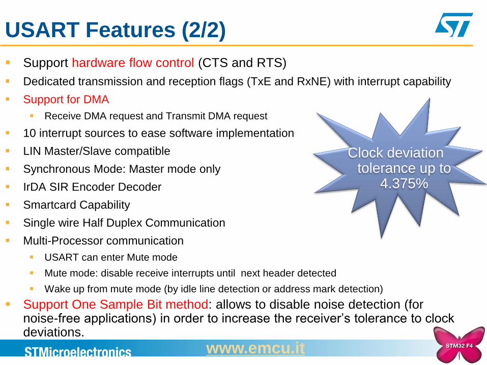
Clock deviation tolerance up to
4.375%
www.emcu.it
SPI Features (1/2)
Up to 3 SPIs: SPI1 on high speed APB2 and SPI2,SPI2 on low speed
APB1
SPI2, SPI3 can work as SPI or I2S interface
Full duplex synchronous transfers on 3 lines
Simplex synchronous transfers on 2 lines with or without a bi-
directional data line
Programmable data frame size :8- or 16-bit transfer frame format
selection
Programmable data order with MSB-first or LSB-first shifting
Master or slave operation
Programmable bit rate: up to 37.5 MHz in Master/Slave mode
NSS management by hardware or software for both master and slave:
Dynamic change of Master/Slave operations
Motorola / TI mode (master and slave operations). www.emcu.it
SPI Features (2/2)
Programmable clock polarity and phase
Dedicated transmission and reception flags (Tx buffer Empty and
Rx buffer Not Empty) with interrupt capability
SPI bus busy status flag
Master mode fault and overrun flags with interrupt capability
Hardware CRC feature for reliable communication (CRC8, CRC16)
Support for DMA
Each SPI has a DMA Tx and Rx requests
Each of the SPIs requests is mapped on a different DMA Stream: possibility
to use DMA for all SPIs transfer direction at the same time
Calculated CRC value is automatically transmitted at the end of data
transfer
www.emcu.it
I2S Features (1/2)
Two I2Ss: Available on SPI2 and SPI3 peripherals.
Two I2Ss extension added for Full-Duplex communication.
Dedicated PLL for high quality audio clock generation.
Simplex/or Full duplex communication (transmitter and receiver)
Can operate in master or slave configuration.
8-bit programmable linear prescaler to support all standard audio sample
frequencies up to 192KHz.
Programmable data format (16-, 24- or 32-bit data formats)
Programmable packet frame (16-bit and 32-bit packet frames).
Underrun flag in slave transmit mode, Overrun flag in receive mode and new
de-synchronization flag in slave transmit/receive mode.
16-bit register for transmission and reception.
Support for DMA (16-bit wide).
www.emcu.it
I2S Features (2/2)
I2S protocols supported:
I2S Phillips standard.
MSB Justified standard (Left Justified).
LSB Justified standard (Right Justified).
PCM standard (with short and long frame synchronization on 16-bit channel
frame or 16-bit data frame extended to 32-bit channel frame)
Master clock may be output to drive an external audio component. Ratio is fixed
at 256xFs (where Fs is the audio sampling frequency).
Note: Since some SPI3/I2S3 pins are shared with JTAG pins, they are not
controlled by the I/O controller and are reserved for JTAG usage (after each
Reset). Prior to configure these pins, the user has to disable the JTAG and use
the SWD interface (when debugging the application), or disable both JTAG/SWD
interfaces (for standalone application).
www.emcu.it
SDIO Features
Cards Clock Management: Rising and Falling edge, 8-bit prescaler,
bypass, power save..
Hardware Flow Control: to avoid FIFO underrun (TX mode) and overrun
(RX mode) errors.
A 32-bit wide, 32-word FIFO for Transmit and Receive
DMA Transfer Capability
Data Transfer: Configurable mode (Block or Stream), configurable data
block size from1 to 16384 bytes, configurable TimeOut
24 interrupt sources to ease software implementation
CRC Check and generation
SD I/O mode: SD I/O Interrupt, suspend/resume and Read Wait
Data transfer up to 48 MHz
www.emcu.it
FSMC Features The Flexible Static Memory Controller has the following main features:
4 Banks to support External memory
FSMC external access frequency is 60MHz when HCLK is at 168Hz
Independent chip select control for each memory bank
Independent configuration for each memory bank
Interfaces with static memory-mapped devices including:
static random access memory (SRAM)
read-only memory (ROM)
NOR/ OneNAND Flash memory
PSRAM
Interfaces parallel LCD modules: Intel 8080 and Motorola 6800
Supports burst mode access to synchronous devices (NOR Flash and PSRAM)
NAND Flash and 16-bit PC Cards
With ECC hardware up to 8 Kbyte for NAND memory
3 possible interrupt sources (Level, Rising edge and falling edge)
Programmable timings to support a wide range of devices
External asynchronous wait control
Enhanced performance vs. STM32F10x
www.emcu.it
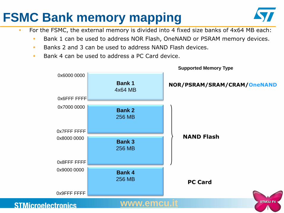
FSMC Bank memory mapping For the FSMC, the external memory is divided into 4 fixed size banks of 4x64 MB each:
Bank 1 can be used to address NOR Flash, OneNAND or PSRAM memory devices.
Banks 2 and 3 can be used to address NAND Flash devices.
Bank 4 can be used to address a PC Card device.
Bank 1
4x64 MB
Bank 2
256 MB
Bank 3
256 MB
Bank 4
256 MB
0x6000 0000
0x7000 0000
0x8000 0000
0x9000 0000
0x6FFF FFFF
0x7FFF FFFF
0x8FFF FFFF
0x9FFF FFFF
Supported Memory Type
NOR/PSRAM/SRAM/CRAM/OneNAND
NAND Flash
PC Card
www.emcu.it
USB 2.0 (OTG FS) - General Features
Fully compliant with Universal Serial Bus Revision 2.0 specification
Dual Role Device (DRD) controller that supports both device and host functions compliant with On-The-Go (OTG) Supplement Revision 1.3
Can be configured as host-only or device-only controller
Integrated PHY with full support of the OTG mode
Full-speed (12 Mbits/s) and low-speed (1.5 Mbits/s) operation (only full speed for device)
Dedicated RAM of 1.25 kB with advanced FIFO management and dynamic memory allocation
www.emcu.it
USB 2.0 (OTG HS) - Main Features
Fully compatible (@ register level) with the full-speed USB OTG peripheral
High-speed (480 Mbit/s), full-speed and low speed operation in host mode and High-speed/Full-speed in device mode
Three PHY interfacing options Internal full-speed PHY (as for FS peripheral)
I2C interface for full-speed I2C PHY
ULPI bus interface for high-speed PHY
DMA support with a dedicated FIFO of 4Kbytes
www.emcu.it
Ethernet MAC 10/100 - Main Features
Supports 10/100Mbits Half/Full-duplex operations modes
MII/RMII PHY interface
Several options for MAC address filtering
IPv4 checksum offload during receive and transmit operation
Dedicated DMA controller with two FIFOs (Rx/Tx) of 2KBytes each Connected as AHB master to system bus matrix
Ethernet Time Stamping support - IEEE1588 version 2
Power management: Wake on LAN with Magic Packet or Wakeup frame
MAC management Counters for statistics
MII loopback mode for debug purpose
www.emcu.it
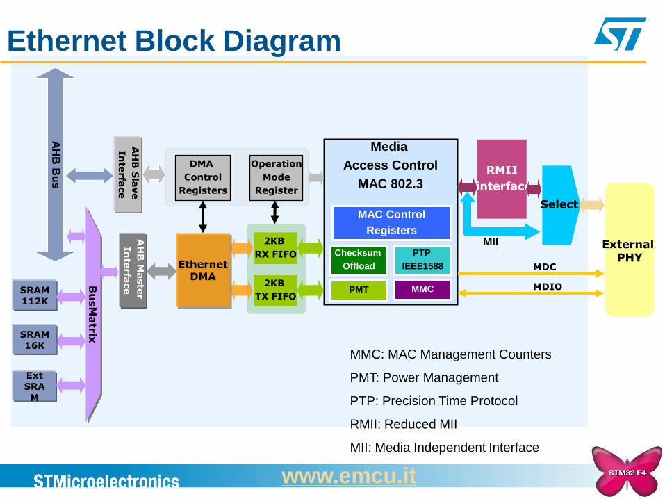
Ethernet Block Diagram
MMC: MAC Management Counters
PMT: Power Management
PTP: Precision Time Protocol
RMII: Reduced MII
MII: Media Independent Interface
Media
Access Control
MAC 802.3
MAC Control
Registers
MMC PMT
PTP
IEEE1588
Checksum
Offload
RMII
interface
Select
MDC
MDIO
External PHY
Operation
Mode
Register
2KB
RX FIFO
2KB
TX FIFO
DMA
Control
Registers
Ethernet DMA
AH
B B
us
AH
B S
lave
In
terfa
ce
AH
B M
aste
r
In
terfa
ce
MII
Bu
sM
atr
ix
SRAM 112K
Ext SRAM
SRAM 16K
www.emcu.it
CAN Features
Dual CAN 2.0 A, B Active w/ Bit rates up to 1Mbit/s, mapped on APB1
Support time Triggered Communication
Three transmit mailboxes w/ configurable transmit priority
Two receive FIFOs with three stages and 28 filter banks shared between CAN1 and CAN2
Time Stamp on SOF reception and transmission
Maskable interrupts for easy software management
Software efficient mailbox mapping at a unique address space
4 dedicated interrupt vectors: transmit interrupt, FIFO0 interrupt, FIFO1 interrupt and status change error interrupt
The two CAN cells share a dedicated 512-byte SRAM memory and capable to work simultaneously with USB OTG FS peripheral
www.emcu.it
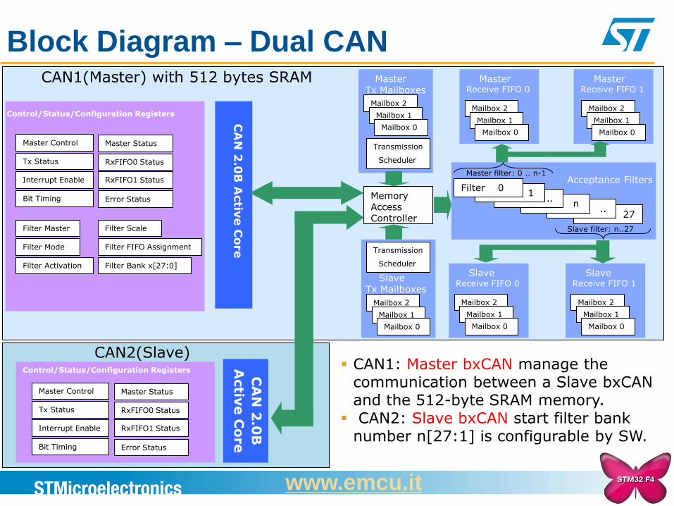
Block Diagram – Dual CAN
CA
N 2
.0B
Activ
e C
ore
CAN1(Master) with 512 bytes SRAM
Control/Status/Configuration Registers
CA
N 2
.0B
Activ
e C
ore
Master Tx Mailboxes
Mailbox 2
Mailbox 1
Mailbox 0
Master Receive FIFO 0
Mailbox 2
Mailbox 1
Mailbox 0
Mailbox 2
Mailbox 1
Mailbox 0
Memory Access Controller
CAN1: Master bxCAN manage the communication between a Slave bxCAN and the 512-byte SRAM memory.
CAN2: Slave bxCAN start filter bank number n[27:1] is configurable by SW.
CAN2(Slave)
Master Control Master Status
Tx Status
RxFIFO1 Status Interrupt Enable
Error Status Bit Timing
Filter Mode
Filter Bank x[27:0]
Filter Master Filter Scale
Filter FIFO Assignment
Filter Activation
RxFIFO0 Status
Control/Status/Configuration Registers
Master Control Master Status
Tx Status
RxFIFO1 Status Interrupt Enable
Error Status Bit Timing
RxFIFO0 Status
Transmission
Scheduler
Transmission
Scheduler
Slave Tx Mailboxes
27
.. n
.. 1
Filter 0
Master Receive FIFO 1
Mailbox 2
Mailbox 1
Mailbox 0
Slave Receive FIFO 0
Mailbox 2
Mailbox 1
Mailbox 0
Slave Receive FIFO 1
Mailbox 2
Mailbox 1
Mailbox 0
Acceptance Filters Master filter: 0 .. n-1
Slave filter: n..27
www.emcu.it
Glossary
ART Accelerator ™ : ST‟s adaptive real-time accelerator
CMSIS: Cortex™ microcontroller software interface standard
MCU: microcontroller unit
DSC: digital signal controller
DSP: digital signal processor
FPU: floating point unit
RTC: real-time clock
MPU: memory protection unit
FSMC: flexible static memory controller
CCM : Core Coupled Memory
www.emcu.it
Recommended