State of Pacific Rim Nanotech.,State of Pacific Rim Nanotech.,specially in Asiaspecially in Asia
-- Green Nanotechnology Green Nanotechnology --
May 18, 2010Shuichi Tahara
NEC Corporation

© NEC Corporation 2010Page 2
Outline
1. Introduction2. Statistics3. Nano-carbon4. Energy devices with nanomaterials5. Si Photonics

© NEC Corporation 2010Page 3
Introduction
© NEC Corporation 2010Page 4
Explosion of Information Traffic and Electric Power Consumption of ICT System
▐ Electric power consumption at data-centers in US was doubled in the past 6 years, reaching to the electric power generated by 5 nuclear power plants.
▐ Information traffic in the Internet will increase 190 times from637Gbps@2007 to120Tbps@2025.
▐ Already, the power consumption of IT system at 2007 is five times larger than that at 2006. The reduction of power consumption must be one of the very urgent issues.
Change of power consumption at data-centersin US from 2000 to 2006
Change of power consumptionof IT system with years
Source : METI “Green IT Initiative”
2006 2007 2008
TVPCServerNWsystem
40%reduction
50%reductionEPA Report
in August of 2007

© NEC Corporation 2010Page 5
To realize sustainable society
▐ Energy and environmental issues have to be solved to realize sustainable society.
▐ Many technologies in broad area have to contribute to do so. ▐ Nanotechnology is one of the most important technologies.
© NEC Corporation 2010Page 6
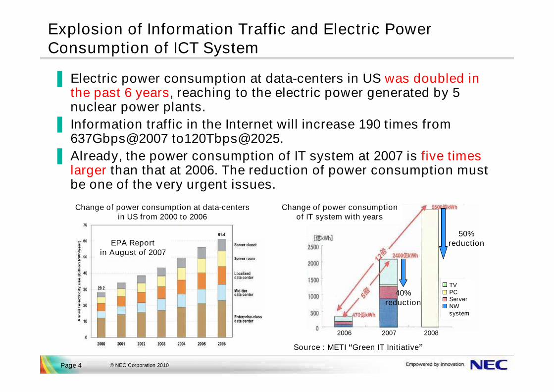
NEC’s Nanotech. Development Strategy▐ Nanotechnology supporting to realize information society
friendly to humans and the earthInformation society friendly to humans
and the earth
Environmental Friendliness
Performance
Pursuing Bit/ECO value by using nanotechnology
Nanotechnology
Quantum bitQuantum bit
20nm
Nano-bridgeNano-bridge
Si photonicsSi photonics
CNTprinted transistorCNTprinted transistor
High performanceInformation processing and ubiquitous safety
Eco-materialEnergy and resource saving productiin
Bio-plasticsBio-plastics
Nano-simulationNano-simulation
Ubiquitous BatteryUbiquitous Battery
Physics and Materials
Quantum Effect(Wave Nature of Particle)
Quantum Effect(Wave Nature of Particle)
Near Field (Trapped Light)
Near Field (Trapped Light)
Self-Organization(Automatic Formation)
Self-Organization(Automatic Formation)
Ballistic Effect(High-speed movement)
Ballistic Effect(High-speed movement)
Surface Effect (Lower Melting Point / High Reactivity)
Surface Effect (Lower Melting Point / High Reactivity)

© NEC Corporation 2010Page 7
Statistics

© NEC Corporation 2010Page 8
OECD: Nanotechnology: An Overview Based on Indicators and Statistics
Share of nanotechnology-related and all publications by country, 1991-2007
Share of nanotechnology-related and all publications of China is larger than that of Japan.1.USA 2.China, 3.Japan, 4.Germany, 5.France
Share of nanotechnology-related and all publications of China is larger than that of Japan.1.USA 2.China, 3.Japan, 4.Germany, 5.France
© NEC Corporation 2010Page 9
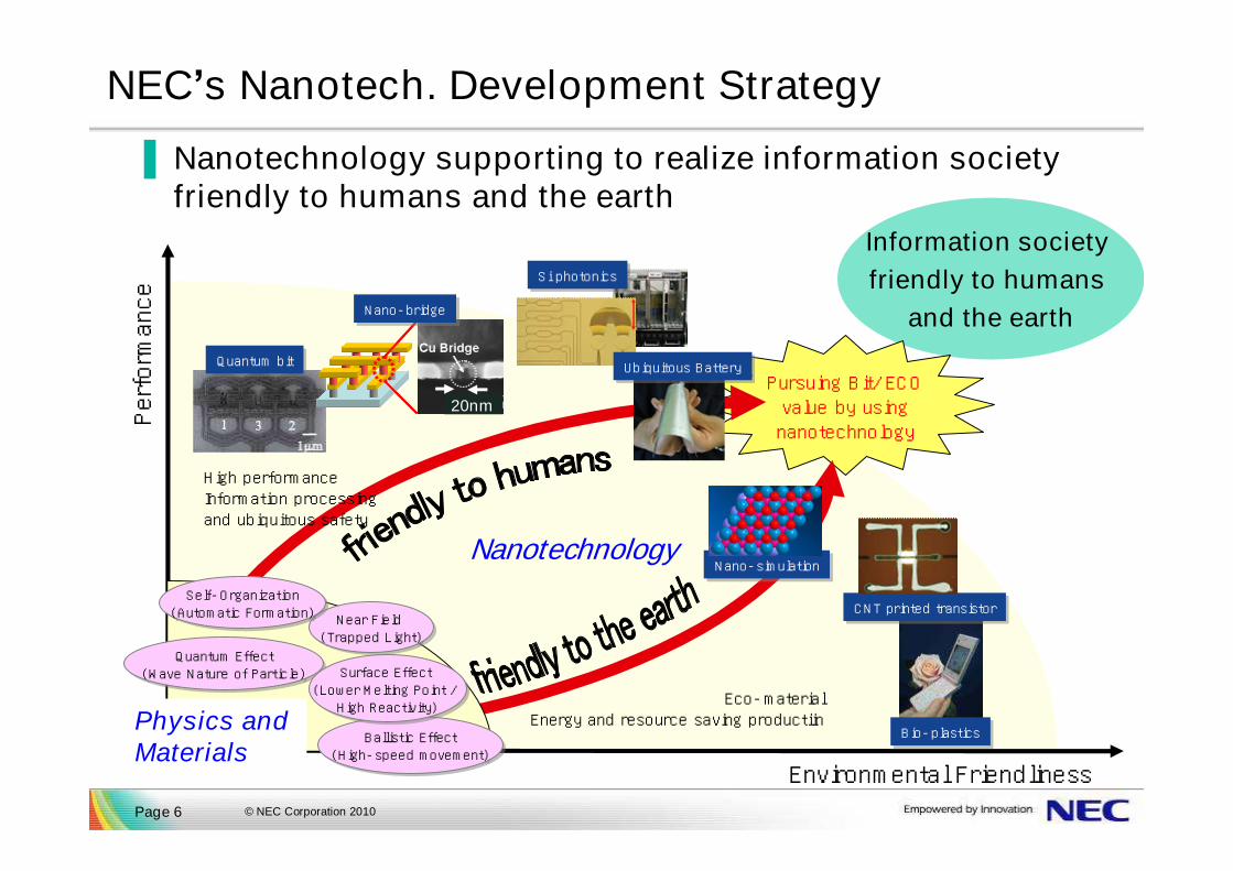
OECD: Nanotechnology: An Overview Based on Indicators and Statistics
Average annual growth rates of nanotechnology-related and all publications by country, 1996-2006
Nanotec. Publications from Asian countries ( Singapore, China, Korea, Chinese Taipei) have grown.
Nanotec. Publications from Asian countries ( Singapore, China, Korea, Chinese Taipei) have grown.
© NEC Corporation 2010Page 10
OECD: Nanotechnology: An Overview Based on Indicators and Statistics
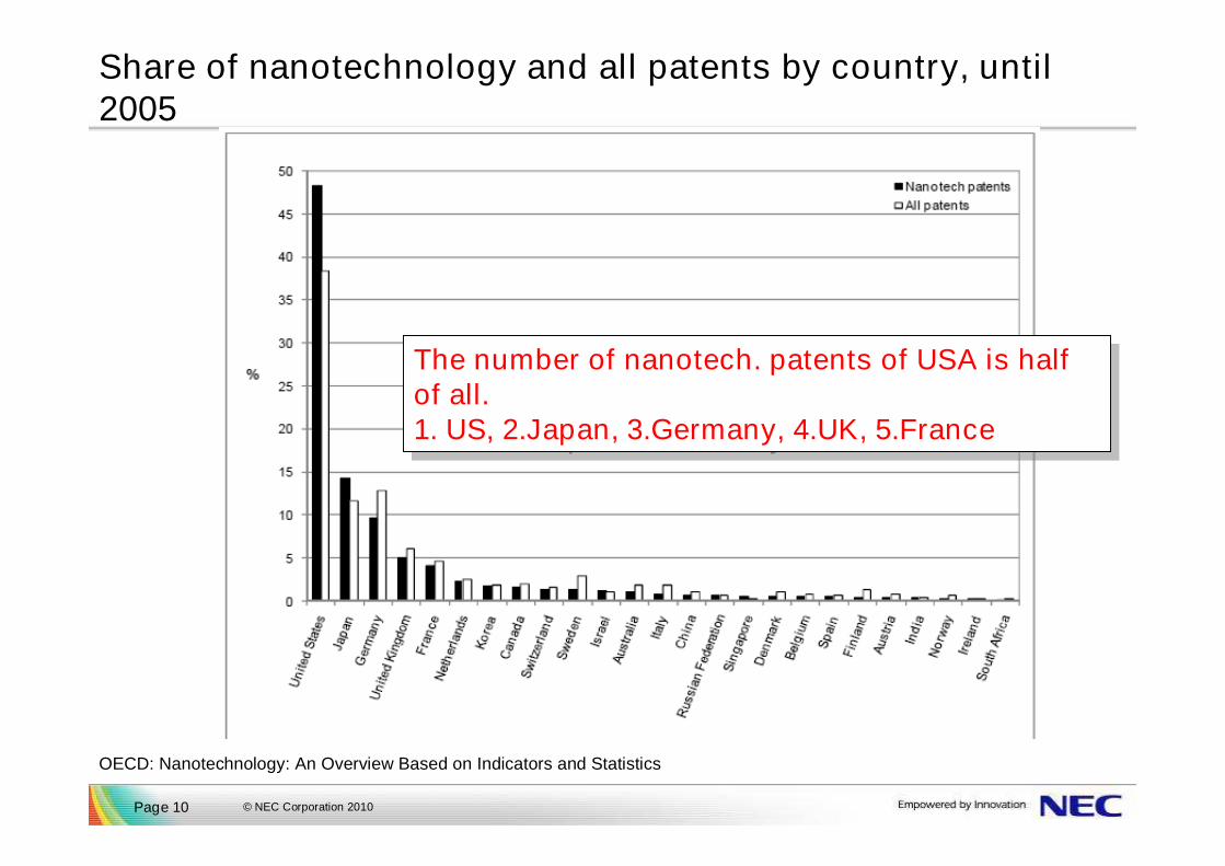
Share of nanotechnology and all patents by country, until 2005
The number of nanotech. patents of USA is half of all.1. US, 2.Japan, 3.Germany, 4.UK, 5.France
The number of nanotech. patents of USA is half of all.1. US, 2.Japan, 3.Germany, 4.UK, 5.France
© NEC Corporation 2010Page 11
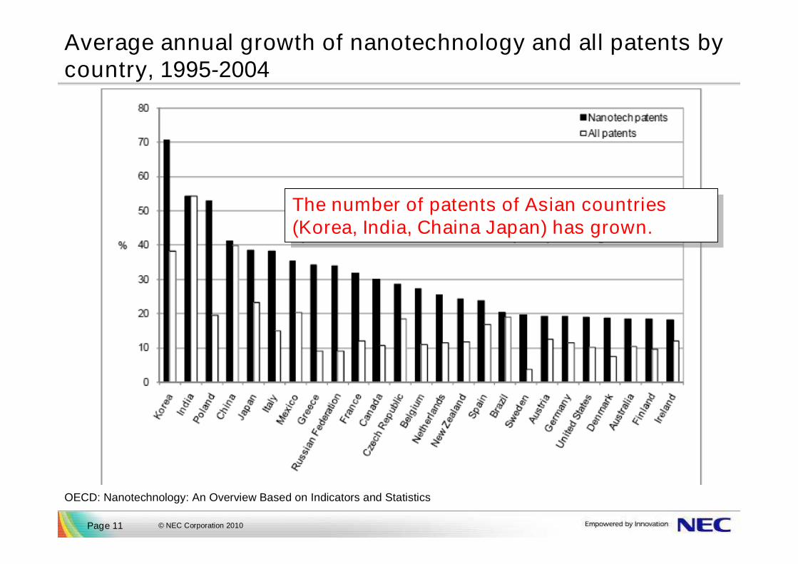
OECD: Nanotechnology: An Overview Based on Indicators and Statistics
Average annual growth of nanotechnology and all patents by country, 1995-2004
The number of patents of Asian countries (Korea, India, Chaina Japan) has grown.
The number of patents of Asian countries (Korea, India, Chaina Japan) has grown.
© NEC Corporation 2010Page 12
Nanocarbon
© NEC Corporation 2010Page 13
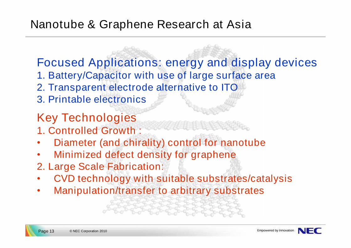
Focused Applications: energy and display devices1. Battery/Capacitor with use of large surface area2. Transparent electrode alternative to ITO3. Printable electronics
Key Technologies1. Controlled Growth : • Diameter (and chirality) control for nanotube• Minimized defect density for graphene2. Large Scale Fabrication:• CVD technology with suitable substrates/catalysis• Manipulation/transfer to arbitrary substrates
Nanotube & Graphene Research at Asia
© NEC Corporation 2010Page 14
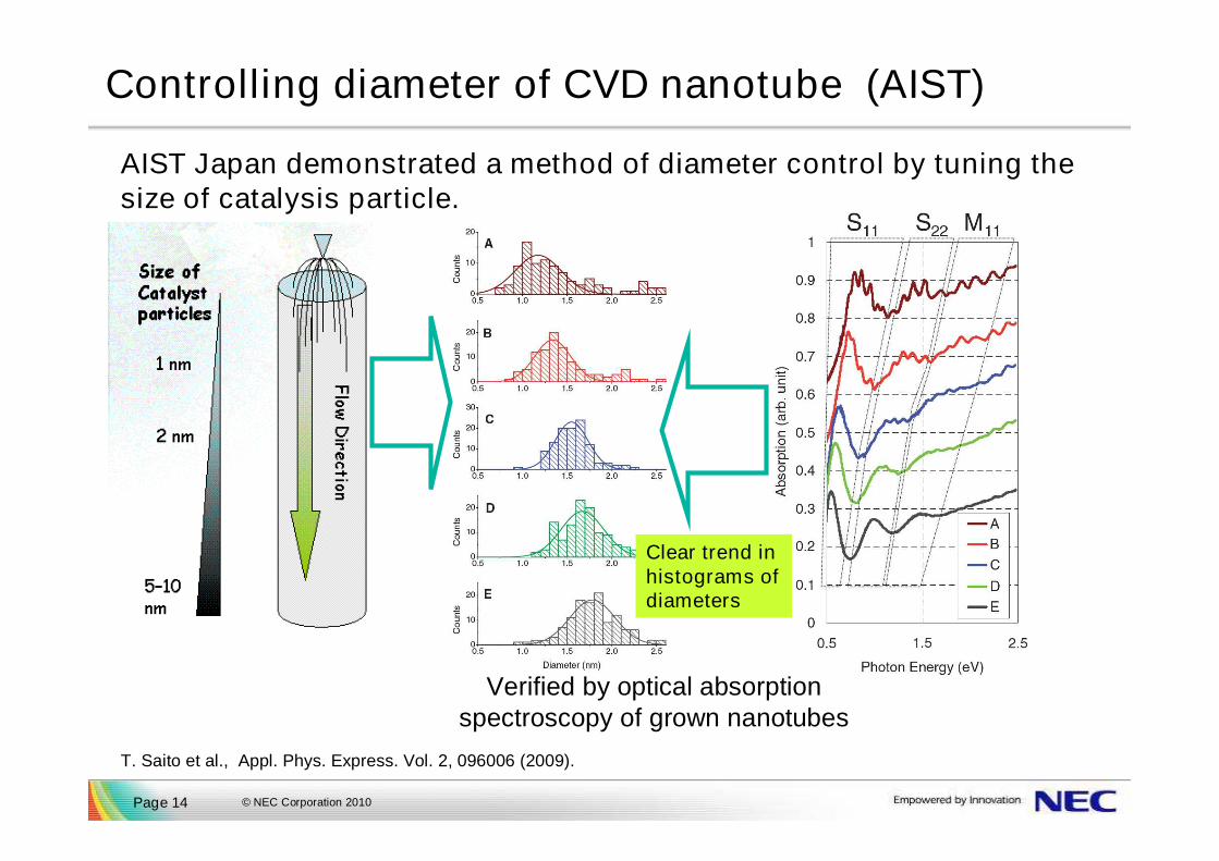
T. Saito et al., Appl. Phys. Express. Vol. 2, 096006 (2009).
AIST Japan demonstrated a method of diameter control by tuning the size of catalysis particle.
Controlling diameter of CVD nanotube (AIST)
Verified by optical absorption spectroscopy of grown nanotubes
Clear trend in histograms of diameters
© NEC Corporation 2010Page 15
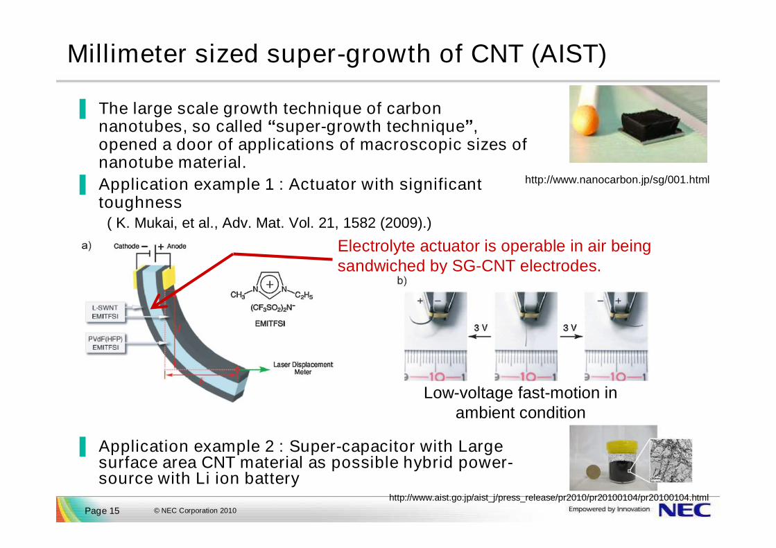
Electrolyte actuator is operable in air being sandwiched by SG-CNT electrodes.
Low-voltage fast-motion in ambient condition
Millimeter sized super-growth of CNT (AIST)
▐ The large scale growth technique of carbon nanotubes, so called “super-growth technique”, opened a door of applications of macroscopic sizes of nanotube material.
▐ Application example 1 : Actuator with significant toughness
( K. Mukai, et al., Adv. Mat. Vol. 21, 1582 (2009).)
http://www.nanocarbon.jp/sg/001.html
http://www.aist.go.jp/aist_j/press_release/pr2010/pr20100104/pr20100104.html
▐ Application example 2 : Super-capacitor with Large surface area CNT material as possible hybrid power-source with Li ion battery
© NEC Corporation 2010Page 16
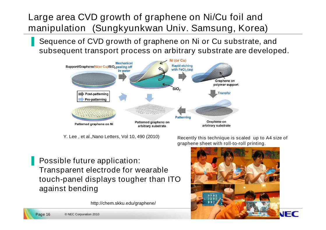
Y. Lee , et al.,Nano Letters, Vol 10, 490 (2010)
Large area CVD growth of graphene on Ni/Cu foil and manipulation (Sungkyunkwan Univ. Samsung, Korea)▐ Sequence of CVD growth of graphene on Ni or Cu substrate, and
subsequent transport process on arbitrary substrate are developed.
http://chem.skku.edu/graphene/
▐ Possible future application: Transparent electrode for wearable touch-panel displays tougher than ITO against bending
Recently this technique is scaled up to A4 size of graphene sheet with roll-to-roll printing.
© NEC Corporation 2010Page 17
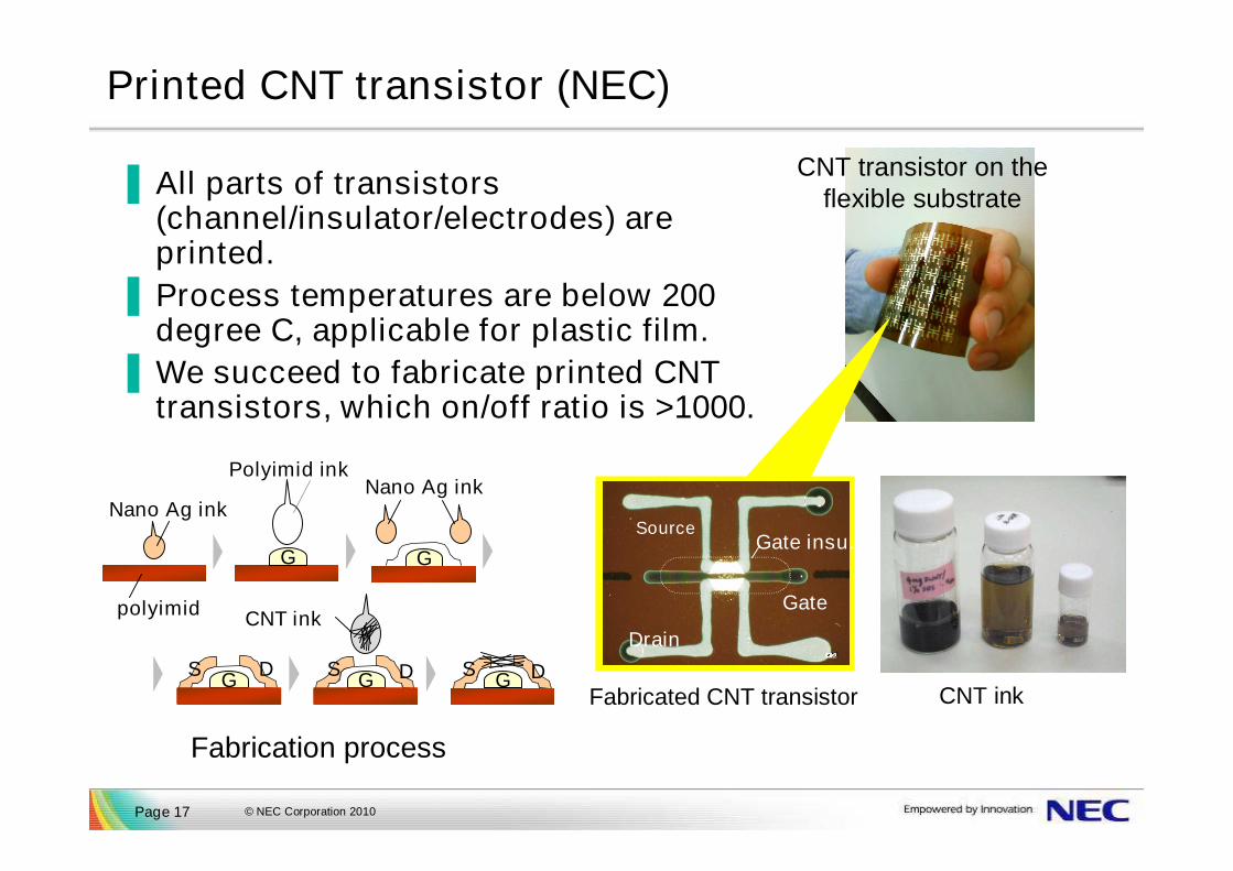
Fabricated CNT transistor CNT ink
CNT transistor on the flexible substrate
Nano Ag ink
polyimid
Polyimid ink
G
Nano Ag ink
G
CNT ink
GS D GS D
G
S D
Fabrication process
Gate insu.
Gate
Source
Drain
Printed CNT transistor (NEC)
▐ All parts of transistors (channel/insulator/electrodes) are printed.
▐ Process temperatures are below 200degree C, applicable for plastic film.
▐ We succeed to fabricate printed CNT transistors, which on/off ratio is >1000.
© NEC Corporation 2010Page 18
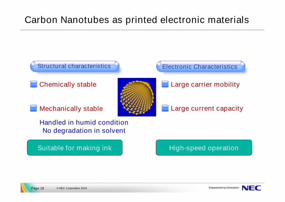
Large current capacity
Large carrier mobility
Mechanically stable
Chemically stable
Suitable for making ink High-speed operation
Handled in humid conditionNo degradation in solvent
Structural characteristics Electronic Characteristics
Carbon Nanotubes as printed electronic materials
© NEC Corporation 2010Page 19
Energy Devices
© NEC Corporation 2010Page 20
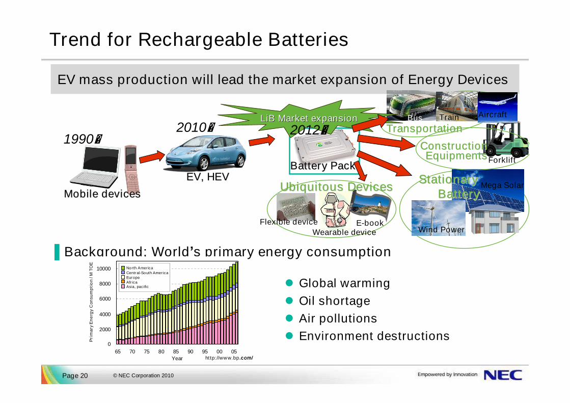
Global warming Oil shortage Air pollutions Environment destructions
▌Background; World’s primary energy consumption
Trend for Rechargeable Batteries
0
2000
4000
6000
8000
10000
65 70 75 80 85 90 95 00 05Year
北米
中南米
欧州
アフリカ
アジア太平洋
Pri
mar
yE
ne
rgy
Con
sum
pti
on
/ M T
OE
North AmericaCentral-South AmericaEuropeAfricaAsia, pacific
http://www.bp.com/
0
2000
4000
6000
8000
10000
65 70 75 80 85 90 95 00 05Year
北米
中南米
欧州
アフリカ
アジア太平洋
Pri
mar
yE
ne
rgy
Con
sum
pti
on
/ M T
OE
North AmericaCentral-South AmericaEuropeAfricaAsia, pacific
http://www.bp.com/
1990~2010~
StationaryStationaryBatteryBattery
Train
Forklift
Mega Solar
Wind Power
ConstructionConstructionEquipmentsEquipments
BusLiBLiB Market expansionMarket expansion
Ubiquitous DevicesUbiquitous Devices
TransportationTransportation
Mobile devicesMobile devicesEV, HEVEV, HEV
Battery PackBattery Pack
2012~
EV mass production will lead the market expansion of Energy Devices
E-bookFlexible deviceWearable device
Aircraft
© NEC Corporation 2010Page 21
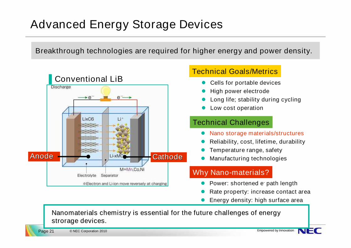
Cells for portable devices High power electrode Long life; stability during cycling Low cost operation
▌Conventional LiB
Advanced Energy Storage Devices
NanomaterialsNanomaterials chemistry is essential for the future challenges of energy chemistry is essential for the future challenges of energy stroragestrorage devices.devices.
Breakthrough technologies are required for higher energy and power density.
CathodeCathodeAnodeAnode
Technical Goals/Metrics
Nano storage materials/structures Reliability, cost, lifetime, durability Temperature range, safety Manufacturing technologies
Technical Challenges
Why Nano-materials? Power: shortened e- path length Rate property: increase contact area Energy density: high surface area
© NEC Corporation 2010Page 22
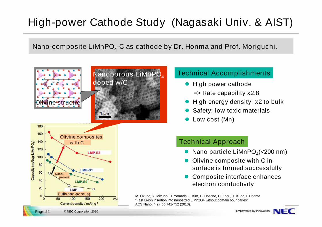
High power cathode=> Rate capability x2.8
High energy density; x2 to bulk Safety; low toxic materials Low cost (Mn)
High-power Cathode Study (Nagasaki Univ. & AIST)
M. Okubo, Y. Mizuno, H. Yamada, J. Kim, E. Hosono, H. Zhou, T. Kudo, I. Honma"Fast Li-ion insertion into nanosized LiMn2O4 without domain boundaries" ACS Nano, 4(2), pp.741-752 (2010).
Nano-composite LiMnPO4-C as cathode by Dr. Honma and Prof. Moriguchi.
Technical Accomplishments
Nano particle LiMnPO4(<200 nm) Olivine composite with C in
surface is formed successfully Composite interface enhances
electron conductivity
Technical Approach
Bulk(non-porous)
Nano-porous
Olivine compositeswith C
Nanoporous LiMnPO4doped w/C
Olivine structre

© NEC Corporation 2010Page 23
Potentiality of Sn-based electrode has been shown
High energy density; 993 mAh/g(ideal)>500mAh/g(current), x1.5 to graphite
60%@60Cycling; Long life as Sn-based material
99% of charge-discharge efficiency
Highly-structured Alloy as Anode (Tokyo Metro. Univ.)
J. Hamagami, K. Hasegawa, K. Kanamura“3D particle assembley in micro-scale by using electrohphoretic micro-fabrication technique”Key Engineering Materials, 314, 7-12(2006).
Lithium ion battery with 3DOM* Sn-Ni alloy as anode by Prof. Kanamura.
Technical Accomplishments
Colloidal particles as template for 3DOM structure
Relaxation of mechanical stress by volume expansion
Technical Approach
*3 Dimensional Ordered Marcoporous
Domain-structured anode was formed using lithographic technique
Suraface
© NEC Corporation 2010Page 24
2
2.2
2.4
2.6
2.8
3
3.2
3.4
3.6
3.8
4
0 20 40 60 80 100
Capacity/ mAh・g-1
Volta
ge/
V
Φ: 150 nm
58 mAh/g106 mAh/gΦ: 300 nm
5 m5 m
NO
OO
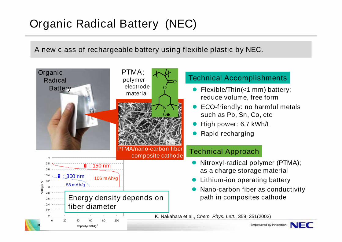
Flexible/Thin(<1 mm) battery: reduce volume, free form
ECO-friendly: no harmful metals such as Pb, Sn, Co, etc
High power: 6.7 kWh/L Rapid recharging
Organic Radical Battery (NEC)
A new class of rechargeable battery using flexible plastic by NEC.
Technical Accomplishments
Nitroxyl-radical polymer (PTMA); as a charge storage material
Lithium-ion operating battery Nano-carbon fiber as conductivity
path in composites cathode
Technical Approach
Energy density depends on fiber diameter
OrganicRadical
Battery
PTMA; polymerelectrodematerial
PTMA/nano-carbon fibercomposite cathode
K. Nakahara et al., Chem. Phys. Lett., 359, 351(2002)
© NEC Corporation 2010Page 25
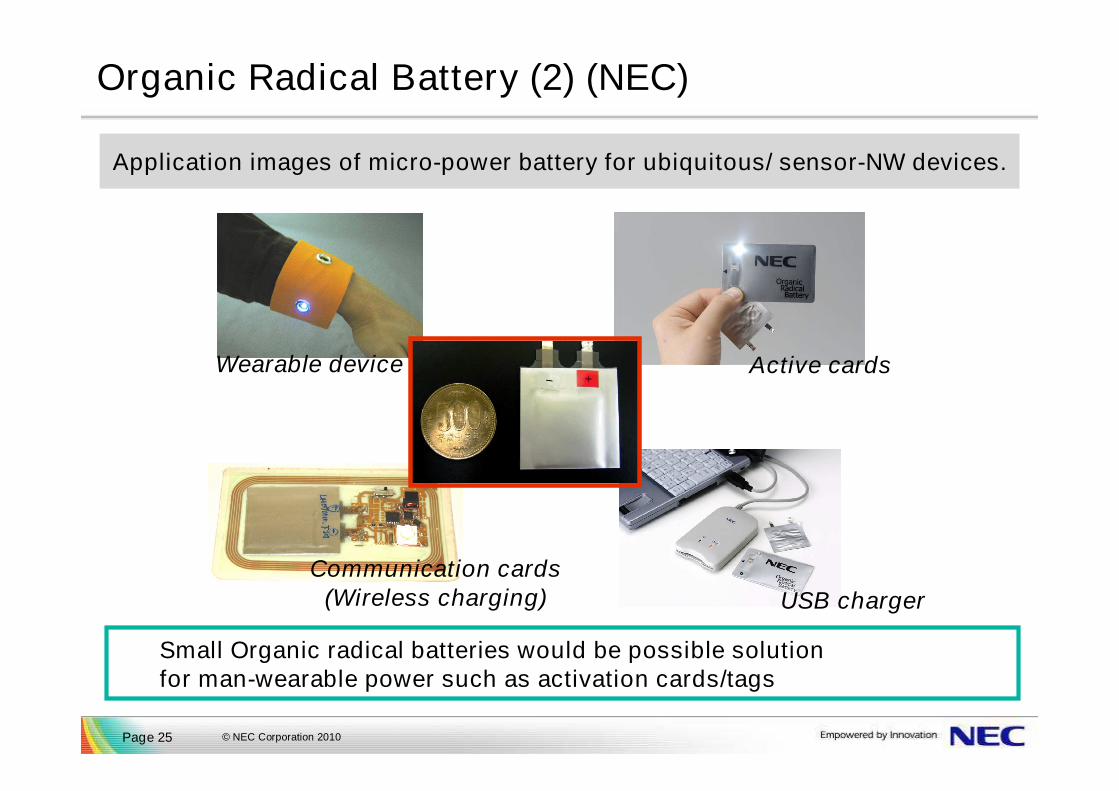
Organic Radical Battery (2) (NEC)
Application images of micro-power battery for ubiquitous/ sensor-NW devices.
Small Organic radical batteries would be possible solutionfor man-wearable power such as activation cards/tags
Active cards
Communication cards(Wireless charging) USB charger
Wearable device

© NEC Corporation 2010Page 26
Si photonics
© NEC Corporation 2010Page 27
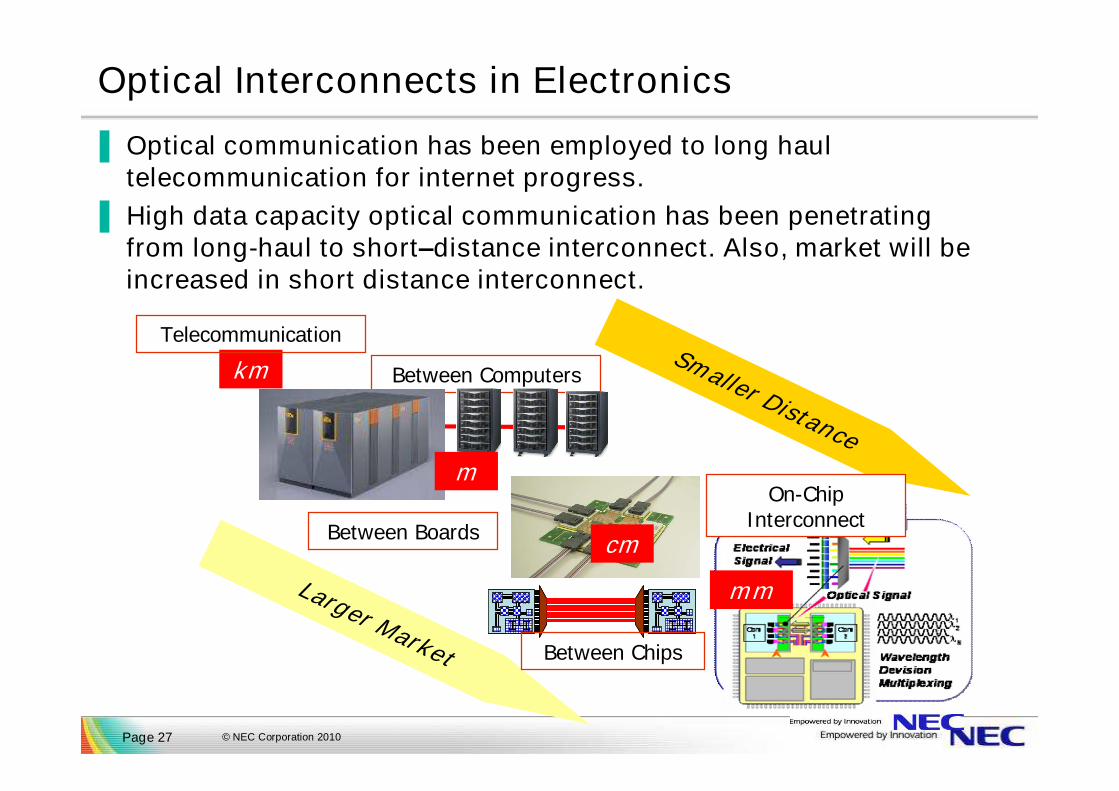
Optical Interconnects in Electronics
Larger Market
Smaller Distance
Between Computers
Between Boards
Between Chips
m
cm
mm
kmTelecommunication
On-Chip Interconnect
▐ Optical communication has been employed to long haul telecommunication for internet progress.
▐ High data capacity optical communication has been penetrating from long-haul to short–distance interconnect. Also, market will be increased in short distance interconnect.
© NEC Corporation 2010Page 28
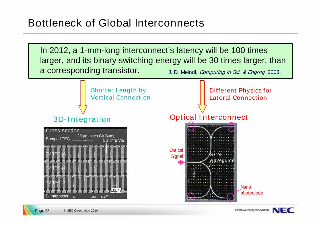
Bottleneck of Global Interconnects
In 2012, a 1-mm-long interconnect’s latency will be 100 times larger, and its binary switching energy will be 30 times larger, than a corresponding transistor. J. D. Meindl, Computing in Sci. & Engrng, 2003.
Si Interposer
TV TEG #1
TV TEG #2
TV TEG #3
Bumped TEG20 µm pitch Cu Bump
Cu Thru Via
10µm
Cross-section
Si Interposer
TV TEG #1
TV TEG #2
TV TEG #3
Bumped TEG20 µm pitch Cu Bump
Cu Thru Via
10µm
Cross-section
3D-Integration
Shorter Length by Vertical Connection
Optical Signal SiON
waveguide
Nano photodiode
Optical Interconnect
Different Physics for Lateral Connection
© NEC Corporation 2010Page 29
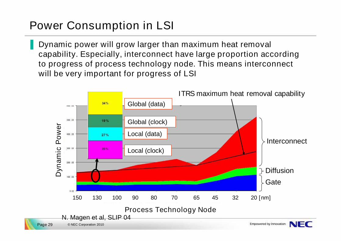
Power Consumption in LSI
Interconnect
Gate
150 130 100 90 80 70 65 45 32 20 [nm]
Dyn
amic
Pow
er
Global (data)
Global (clock)
Local (data)
Local (clock)
N. Magen et al, SLIP 04
Diffusion
ITRS maximum heat removal capability
Process Technology Node
▐ Dynamic power will grow larger than maximum heat removal capability. Especially, interconnect have large proportion according to progress of process technology node. This means interconnect will be very important for progress of LSI
© NEC Corporation 2010Page 30
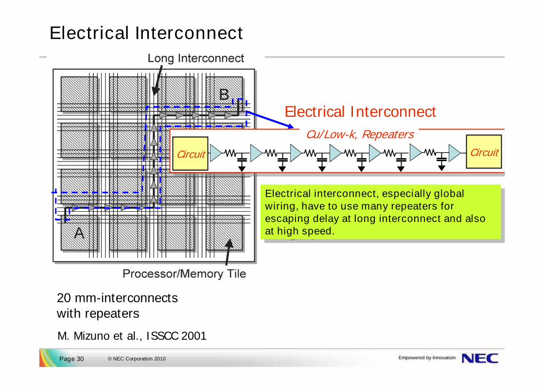
Electrical Interconnect
Electrical Interconnect
M. Mizuno et al., ISSCC 2001
20 mm-interconnects with repeaters
Cu/Low-k, リピーター
電子回路 電子回路Circuit
Cu/Low-k, RepeatersCircuit
Electrical interconnect, especially global wiring, have to use many repeaters for escaping delay at long interconnect and also at high speed.
Electrical interconnect, especially global wiring, have to use many repeaters for escaping delay at long interconnect and also at high speed.
© NEC Corporation 2010Page 31
Cu/Low-k, リピーター
電子回路 電子回路Circuit
Cu/Low-k, RepeatersCircuit
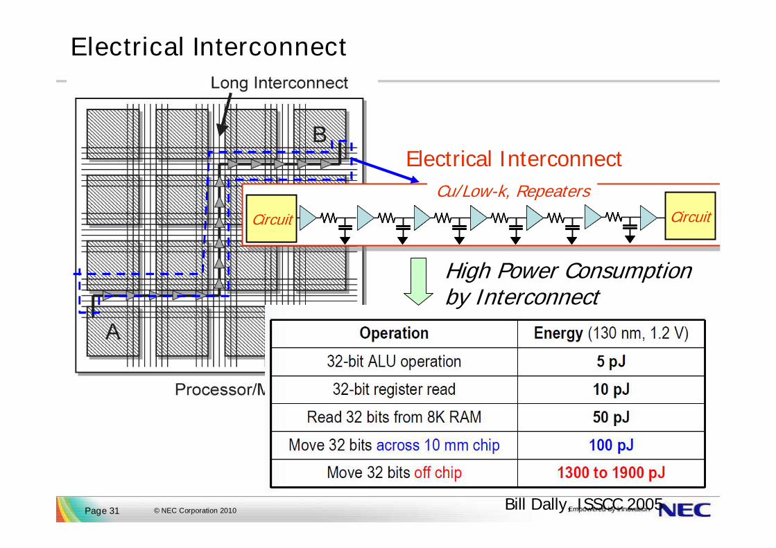
Bill Dally, ISSCC 2005
High Power Consumption by Interconnect
Electrical Interconnect
Electrical Interconnect
© NEC Corporation 2010Page 32
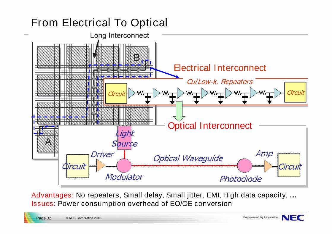
From Electrical To Optical
Cu/Low-k, リピーター
電子回路 電子回路Circuit
Cu/Low-k, RepeatersCircuit
Optical Interconnect
Advantages: No repeaters, Small delay, Small jitter, EMI, High data capacity, …Issues: Power consumption overhead of EO/OE conversion
Electrical Interconnect

© NEC Corporation 2010Page 33
IEEE Journal of Selected Topics in Quantum Electronics
Institute of Microelectronics, Singapore
Si modulators and Ge detectors aremonolithically integrated.Si modulator achieves 10Gbps operation at 2-mm-long device.
Shanghai Institute of Microsystemand Information Technology (SIMIT) & Institute of Semiconductor, Chinese Academy of Sciences
Si modulator achieves 10Gbps operation. http://www.sim.cas.cn/xwzx/kyjz/201003/t20100323_2804854.html
Silicon Phtonics activities in Asia
Si photonics are investigated by using 6 & 8-inch CMOS Lines in Singapore and Shanghai.
© NEC Corporation 2010Page 34
1
10
100
1000
10000
100000
1000 100 10 1
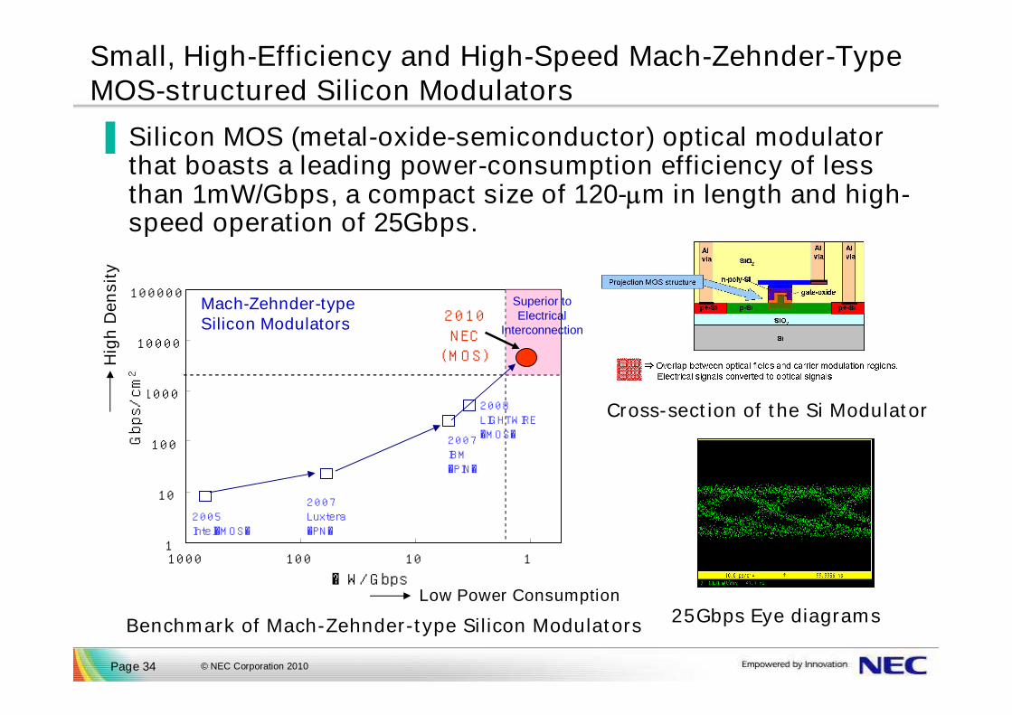
Mach-Zehnder-typeSilicon Modulators
2005Intel(MOS)
2007Luxtera(PN)
2007IBM(PIN)
mW/Gbps
Gbps/cm2
2010NEC(MOS)
Superior toElectrical
Interconnection
2008LIGHTWIRE(MOS)
Low Power Consumption
Hig
h D
ensi
ty
Benchmark of Mach-Zehnder-type Silicon Modulators 25Gbps Eye diagrams
Small, High-Efficiency and High-Speed Mach-Zehnder-Type MOS-structured Silicon Modulators
Cross-section of the Si Modulator
▐ Silicon MOS (metal-oxide-semiconductor) optical modulator that boasts a leading power-consumption efficiency of less than 1mW/Gbps, a compact size of 120-m in length and high-speed operation of 25Gbps.
© NEC Corporation 2010Page 35
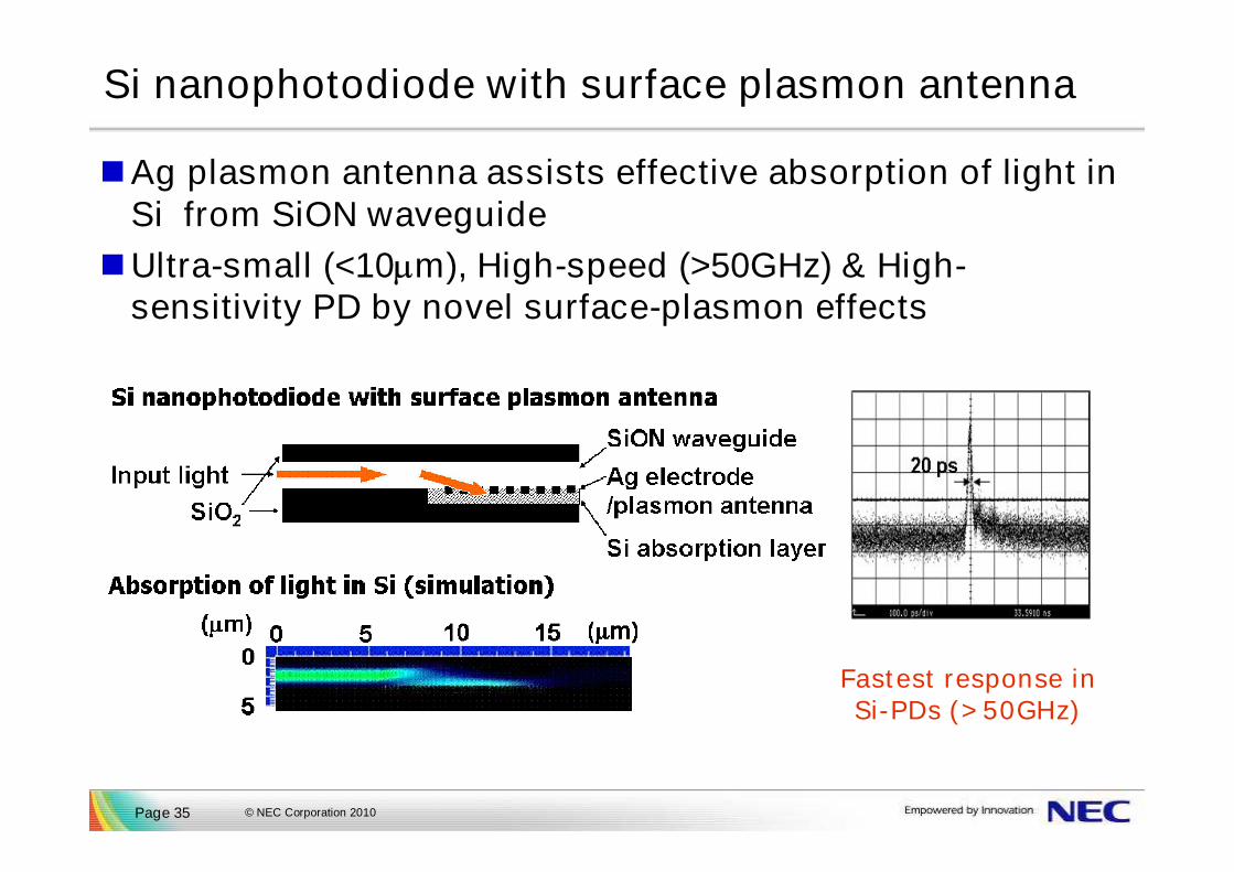
Fastest response in Si-PDs (>50GHz)
Si nanophotodiode with surface plasmon antenna
Ag plasmon antenna assists effective absorption of light in Si from SiON waveguide
Ultra-small (<10m), High-speed (>50GHz) & High-sensitivity PD by novel surface-plasmon effects
© NEC Corporation 2010Page 36
Summary
▐ Nanotechnologies are very important to realize the future sustainable society.
▐ Nanocarbon, such as CNT and graphene, electronics are useful for printable electronics, large-area electronics
▐ Nano-material technologies are essential to improve the capacity, stability and reliability for energy and environmental devices.
▐ Si photonics is one of the key technologies for interconnections in the future IT/NW systems.

Recommended